

Page 1

LQ-1500
SERVICE MANUAL
Printed on Recycled Paper
a9
®
EPSON
Page 2

1.1 Product Overview
1.2 LQ-1500 Interface Overview
1 .3Specifications
1 .4Major Components
2.1
General..
..............................................................................................................................................
2.2 ConnectIon Diagram
2.3 Connector Pin Assignment
Connector on UXMCL circuit board..
2.3.1
Connector on UXDRV circuit board..
2.3.2
Connector on UXPS/PSU 24E circuit board..
2.3.3
2.4
Electrical Circuit
Power circuit
2.4.1
2.4.2 Reset circuit
Sensor circuit..
2.4.3
Carriage motor control circuit..
2.4.4
LF motor control circuit
2.4.5
2.4.6 Head driver circuit
Auto sheet load circuit
2.4.7
Other function..
2.4.8
2.5 Printer Mechanism..
Operation
2.5.1
................................................................................................................................
.....................................................................................................................................
..............................................................................................................................
...........................................................................................................................
..................................................................................................................
.................................................................................................................
...............................................................................................................................
........................................................................................................................
.....................................................................................................................
.........................................
.............................................................................................................................
................................................................................................................................
TABLE OF CONTENTS
CHAPTER 1
GENERAL
...............................................................................................................
CHAPTER 2
PRINCIPLES OF OPERATION
.................................................................................................................
.........................................................................................
.......................................................................................
...........................................................................
.............. 2-13
......................................................................
.............................................................................................................
..............................................................................................................
..............................................................................
...................
1-1
1-1
1-1
1-4
2-1
2-1
2-3
2-3
2-8
2-12
.......... 2-13
2-22
2-22
......
2-26
2-34
2-37
2-39
2-40
2-41
2-41
CHAPTER 3
OPTIONAL EQUIPMENT
3.1 Centronics Compatible Parallel Interface
Introduction
3.1 .1
Specification.. ................................ ..............................
3.1 .2
Operating principal
3.1 .3
Block diagram..
3.1.4
Circuit diagram
3.1 .5
Component layout ...............
3.1 .6
3.2 RS-232C/Current Loop Interface..
lntroductron ............
3.2.1
Specification.. ........
3.2.2
Operating principal ....................................... ....................................................
3.2.3
Block diagram....................................... ..... .............................................................................
3.2.4
Circuit diagram.. ......................... .......... .....
3.2.5
Component layout ....................................................................................................................
3.2.6
3.3 IEEE-488 Interface..
Introduction .......... ........ .............................................................
3.3.1
Specification.. ..... .........
3.3.2
IEEE-488 operatronal parameters.............................
3.3.3
IEEE-488 functional commands .........................................
3.3.4
Block diagram..... .............................. .................
3.3.5
Circuit diagram.. ................................... .......
3 3.6
Component layout ................................
3.3.7
3.4 Single Bin Cut Sheet Feeder (# 8334), Double Bin Cut Sheet Feeder (# 8344)
Introduction ......... ...........................
3.4.1
Specifications.. ..... ........ .......... ...... .................................................
3.4.2
Principle of operation.. ........... ...................................................................
3.4.3
Disassembly and assembly..
3.4.4
Troubleshooting.. .........................................
3.4.5
Preventive maintenance ...... .........................................................................................
3.4.6
.............................................................................................................................
..................................................................................................................
...........................
......... ............................. .........
.,.,.,
..........................................................................................................
...
....... ....................................
...................... ........ ........ .....
...........................................................................................
...................................................... 3-1
...
....
..............................
..............................................................
.................................................................................................. 3-8
...................................
....................................................................................................
...
....
............................................................
..............
.....................................................
...............................................
..........................................................................
....
........
...
..................................................................
....
..............................................................
.............................................................
......................................................................
................................................
....
..............................................
..... .................................................... 3-26
........ ....................................... 3-27
....................................................... 3-29
........................................ 3-42
3-1
3-1
3-4
3-6
.......
3-7
3-9
3-9
..........
3-9
......................
........................ 3-20
..................................... 3-22
.............. 3-32
.................................
.......... ..................
....
........................ 3-36
...........
..........
3-15
3-19
3-21
3-22
3-22
3-31
3-33
3-33
3-34
3-52
3-60
Page 3

CHAPTER 4
DISASSEMBLY/ASSEMBLY AND ADJUSTMENT
4.1
General..
4.2 Tools and Measuring Instruments
4.3 Disassembly and Assembly..
4.3.1 Removal of upper case
4.3.2 Removing the circuit boards..
4.3.3 Removal of Model-3660 printer mechanism..
4.3.4 Removal of fan set UB (head cooling fan).
4.3.5 Removal, installation and adjustmnent
4.3.6 Removal of CPU and ROM.
4.3.7 Adjustment of print alignment (backlash)
4.4 Adjustment.........................
4.4.1 MTS and DTS sensor board adjustment..
4.4.2 H.P. sensor board adjustment
4.4.3 Backlash of the carnage motor and belt driving pulley..
4.4.4 Backlash of the paper feed motor and
............................ ...............................................................................................
...................... ........................ 4-1
........................... 4-6
.............................................. .......................................................
.... ...... .......................................... .....................................................
.......
....
of print head..
paper feeding reduction gear
................................................... ......................................................
...
.................................................
....................................... ........................... .......................
..............................................
.....................................................................
...
...... ........ ........................................................................ 4-9
.....................................................................
..................................................................................
..................................................................................................
............................................................
........... ................................. ......................................................
CHAPTER 5
TROUBLESHOOTING
5.1 Entry of Troubleshooting
5.2 Check-out Procedure
5.3 Unit Repair Flow Chart (UXMCL).
5.4 Unit Repair Flow Chart (UXDRV)
5.5 Unit Repair Flow Chart (UXPS).
5.6 Unit Repair Flow Chart (IUPIF)
......... ................ ..................................................
..... ....... ..... ........ ..........................................
....................
......................
.......... ..... ........................................................................
........ ................................................................................................
...... ....................................................................................................
............................. ......... ....................................................
.,
.,.,
4-1
4-2
4-2
4-3
4-6
4-7
4-10
4-12
4-12
4-1 4
4-15
4-16
5-1
5-4
5-18
5-33
5-40
5-42
CHAPTER 6
MAINTENANCE
6.1
Maintenance
6.1 .1
Cleaning..
6.1 .2 Inspection..
6.2 Lubrication..
6.2.1 Lubricants..
6.2.2 Lubrication requirement
6.2.3 Lubrication
6.2.4 Adhesive application requirements
6.2.5 Adhesive application points..
6.2.6 Lubricants and adhesives list..
....................... ........ ......... ..... ...............................................................................
............
................
.............................
........... ...... ...... .......... ........ ........................................................................
point.. .....................................................................................................................
... ...
................ ...... ........................
...
.... ....
............................................................................................
....
.....................................................................................................
.......................................................................................................
.................................... .......
.............................................
...............................................................................................
...........................................
............. .............................
....
........... ...............................
....
CHAPTER 7
APPENDIX
List of principal IC’s..
Description of principal IC's
Exploded diagram for LQ-1500..
Lubrication and adhesive application points drawing A
Lubrication and adhesive application points drawing B.. ............................................................................
Lubrication and adhesive application points drawing C
UXMCL circuit diagram
Component layout of UXMCL board.
UXDRV circuit diagram..
Component layout of UXDRV board..
UXPS circuit diagram..
Component layout of UXPS board..
PSU 24E circuit diagram..
Component layout of PSU
UXFIL circuit diagram ..................... ..........................................................................................................
II
................. ...... ......................................................................................................
.......
...............................................................................................................................
............................................................................................................................
............................. .................................................................................................
...........................................................................................................................
24E board ........................................................................................................
...
........................................................................................................
................................................................................................................
.............................................................................
..............................................................................
.........................................................................................................
.........................................................................................................
............................................................................................................
6-1
6-1
6-1
6-2
6-2
6-2
6-2
6-3
6-3
6-4
7-1
7-2
7-35
7-36
7-37
7-38
7-39
7-40
7-41
7-42
7-43
7-44
7-45
7-46
7-47
Page 4

INTRODUCTION
This technical manual describes the principle of mechanical and electrical
operations, as well as the maintenance and repair procedures, of the EPSON
LO-1500 Dot Matrix Printer.
Chapters 4 through 6 of the manual deal with the fundamental troubleshooting, maintenance and repair of the LO-1500.
For detail on the disassembly, assembly, troubleshooting and maintenance of
the Model-3660 Printer Mechanism, refer to the separately published “Technical Manual of EPSON Model-3660”.
* The contents of this manual are subject to change without notice
Ill
Page 5

CHAPTER 1
GENERAL
1 .1
Product Overview..
1.2 LQ-1500 Interface Overview
1.3 General Specifications
1 .4
Major Components..
.................................................................................
...........................................................................
...............................................................................
................................................................
1-1
1-1
1-1
1-4
Page 6

1 .1 Product Overview
The LO-1500 is a serial terminal printer, featuring 200 CPS, bi-directional printing (draft pica mode) with
logical seeking capability, and 24 x 24 dot-matrix character formation.
which permit connection of the printer to various computers are optional.
cartridge type, which can be set snugly into the housing.
Should maintenance or repair be required, the printer mechanism and circuit boards of the LQ-1500 are
readily replaceable. The technician can perform maintenance and repair quite easily by referring to this
manual.
All interfaces for the LO-1500
The interface circuit boards are
1.2 LQ-1500 Interface Overview
(1) Centronics-compatible, parallel interface
This standard communication link permits data exchange with many computers without modification
or addition of other peripheral devices.
(2) RS-232C/Current Loop Serial Interface
A 20 mA current loop type, serial interface which permits the printer to receive data at a bit rate
ranging from 75 to 19200 BPS.
(3) IEEE-488 Interface
An optional interface which permits parallel communication between the printer and any computer or
measuring
488-l975.
instrument which is equipped with bus structure conforming the IEEE-488 Std.
1.3 General Specifications
(1 )
Printing Method . . . . . . . . . . . . . . . . . . . . . . . .._......
(2)
Character . . . . . . . . . . . . . . . . . . . . . . . . . . . . . . . . . . . . . . .
(3) Character Structure
Character
Draft
LO
ProportIonal
(4) Character Size SeeTable1. on the page 1-3
(5) Column Width..
(6)
Print Speed
(7) Paper Feed
(8) Paper
@
Cut sheet
Paper width ..,,._..........................
Paper thickness .
Weighing .._.............. .
................................ See Table 1. on the page 1 - 3.
........................................
.....................................
Impact dot matrix
1.
Draft
2. Near letter quality (LO)
3. Proportional (standard)
4. Multi-font (with option card)
5. Super/subscript in each above character style. (1 to 4.)
Normal
9x17
font
15 x 17
37x17
See Table 1. on the page 1 - 3.
Friction feed (standard)
Adjustable tractor feed (option)
182 mm to 364 mm
0.06 mm to 0.1 mm
45 kg to 70 kg (52 to 82 g/m*)
font
font
Super/Subscript
7
x
11
font
11
x
11
font
23 x
1 1
font
1-1
Page 7
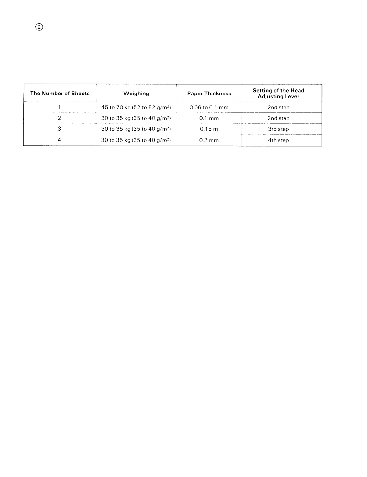
@
Fanfold paper
101
paper width
Copies
Paper thickness and Weight
Notes:
1. Jointing finish of copies should be point or line pasting.
2. Release the friction feed during the tractor feed operation.
3. Set the head adjusting lever as shown in above table.
However, adjust the step setting within range +1 step, depending on print density.
mm to 406 mm
4 sheets max. (include original)
Paper Insertion
(9)
(1 0) Line Spacing
Print Direction................................
(1 1)
(1 2) Line Feed Repeat Rate
Ribbon..
(1 3)
...........................................
...........................
..................................
....................
Rear
1/6”, 1/8” or programmable
Bidirectional printing with logical seeking.
In bit image and double-strike mode, unidirectional printing from
left to right is selected when the power is ON.
Bidirectional printing is also possible using ESC U.
120 ms/line (when 1/6” line feed is performed intermittently)
100 ms/line (when 1/6” line feed is performed continuously)
Exclusive cartridge ribbon (Black)
1-2
Page 8
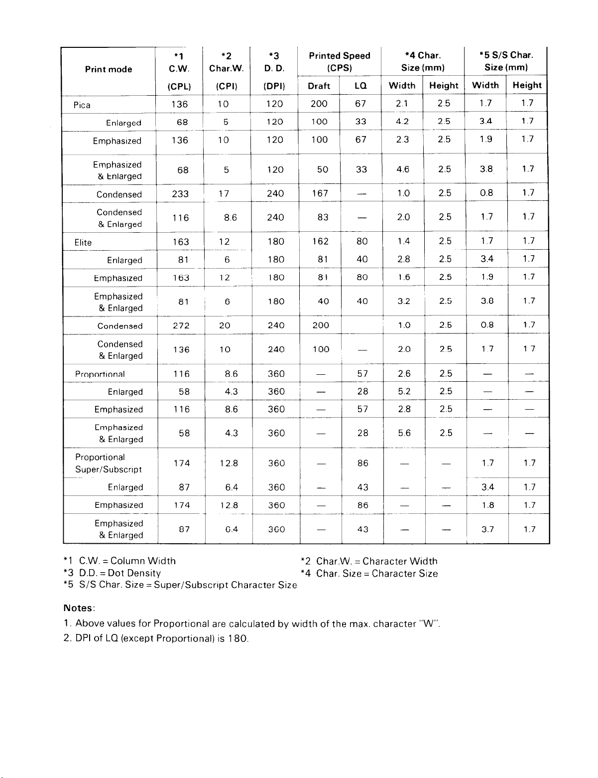
Table 1
1-3
Page 9
1.4 Major Components
The LQ-1500 consists, in a broad classification, of the following five major components
(I ) Housing
(2) Model-3660 printer mechanism
(3) Control circuit boards
(4) Interface circuit boards
(5) Power supply circuit boards
The housing of the LQ-1500 consists of an upper case and lower case. The lower case is designed to
facilitate mounting of the following components.
Circuitry for the LQ-1500 is located on five different boards: the UXFIL and UXPS/PSU 24E boards which
house the power supply; the UXMCL board, which contains most of the control circuitry; the UXDRV,
which handles print mechanism drive circuitry, and a interface board (IUPIF or IURS or IUIE) which serves
as computer interface.
1-4
Page 10
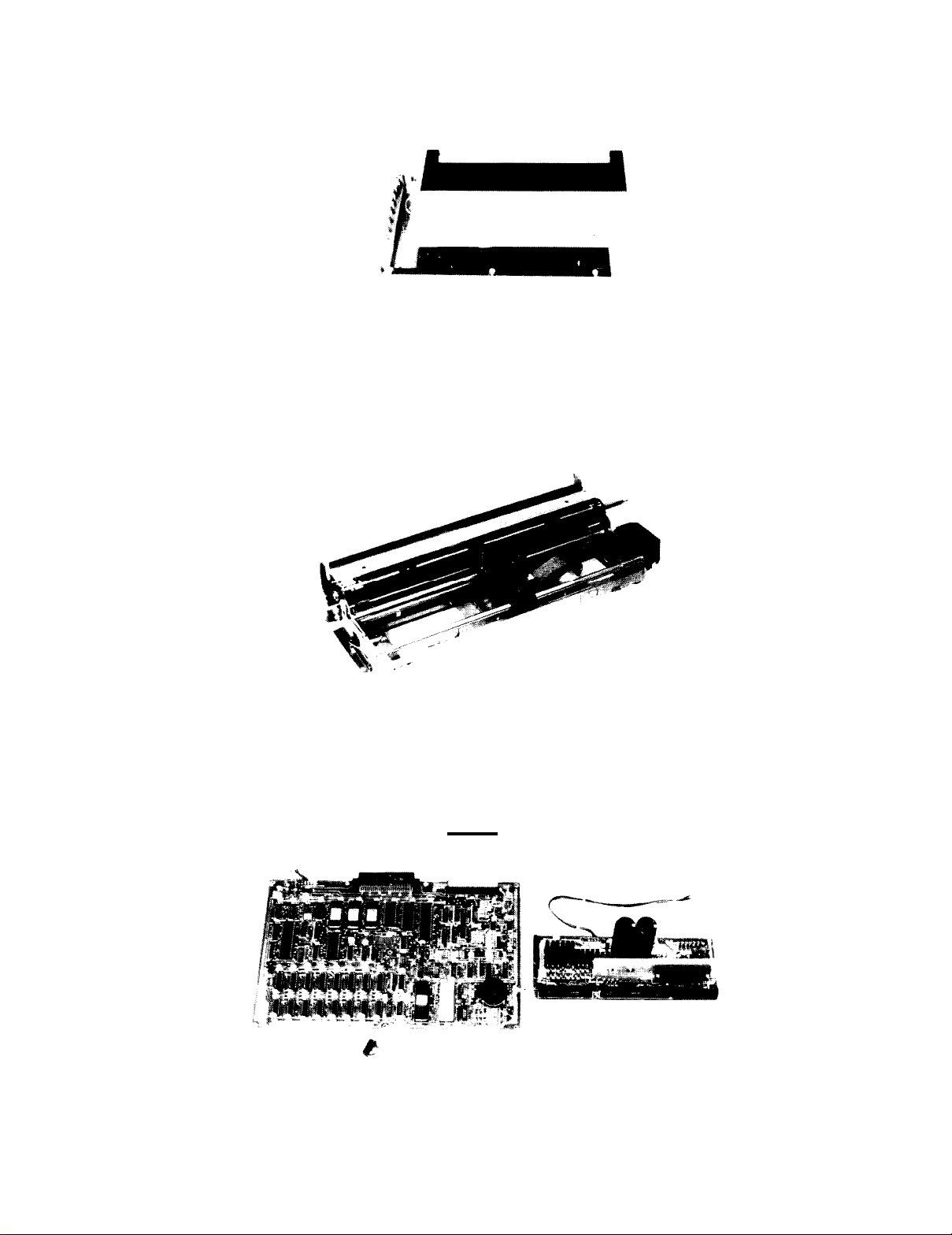
(1) Housing (Fig. 1 .1)
Fig 1 .1 Upper and lower cases
(2) Model-3660 printer mechanism (Fig. 1.2)
The mechanism is an assembly of all the mechanical components including two stepper motors, a print
head, a ribbon feeding mechanism, a carriage assembly, sensors, and a frame section. One stepper
motor operates the print head carriage,
while the other works as the paper feed motor. The
Model-3660 is designed to permit easy maintenance.
‘Fig. 1.2 Model-3660 printer mechanism
(3) Contrl circuit boards (Fig. 1.3)
The control circuit is distributed between two circuit boards, the UXMCL and UXDRV.
The UXMCL circuit board performs the central processing, and the UXDRV circuit board drives the
Model-3660 printer mechanism.
Fig. 1.3 Control circuit boards
1-5
Page 11
(4) Interface circuit boards (Fig. 1 .4)
An interface circuit board exchanges data between the host computer and UXMCL circuit board.
Fig. 1.4 Interface circuit board
(5) Power supply circuit boards (Fig. 1.5)
The power supply circuit of the LQ-1500, consists of two major components, the UXFIL and UXPS/
PSU 24E circuit boards. Both circuit boards are located in the rear righthand corner. The UXPS/PSU
24E circuit board supplies DC +24V, +12V, -12V and +5V to the control circuit and the interface circuit.
Fig 1.5 Power supply circuit board (100/120V version)
Fig 1.6 Power supply circuit board (220/24OV version)
1-6
Page 12

CHAPTER 2
PRINCIPLES OF OPERATlON
....................................................
2.1 General
2.2 Connection
2.3 Connector Pin Assignment
2.3.1 Connector on UXMCL circuit board
2.3.2 Connector on UXDRV circuit board
2.3.3 Connector on UXPS/PSU 24E circuit board..
2.4 Electrical Circuit
2.4.1 Power circuit
2.4.2 Reset circuit
2.4.3 Sensor circuit.. ............................................................................
2.4.4 Carriage motor control circuit..
2.4.5 LF motor control circuit
2.4.6 Head driver circuit.
2.4.7 Auto sheet load circuit
2.4.8 Other function
2.5 Printer Mechanism
2.5.1 Operation
...............................................
Diagram ............................................................................
.................................................................
.........................................
.........................................
.........................
...................................................................................
..............................................................................
................................................................................
................................................
.............................................................
....................................................................
..............................................................
............................................................................
...............................................................................
....................................................................................
2-1
2-1
2-3
2-3
2-8
2-12
2-13
2-13
2-22
2-22
2-26
2-34
2-37
2-39
2-40
2-41
2-41
Page 13
2.1 General
This chapter provides the descriptron of signals at the various connectors electrically interconnecting such
major components as printer mechanism, control circuits, interface circuit, power supply circuit, and control pannel of EPSON LO-1500 Terminal Printer, and explains the operating principles of the various mechanism around the electric circuit of the printer.
2.2 Connection Diagram (Fig. 2.1)
Fig. 2.1 Connection diagram
2-1
Page 14
The CPU Z-80A provides overall control of the LQ-1500. In addition the LQ-1500 is supported by two
slave CPUs: the 8042(8742), which controls the carriage motor; the 8041(8741), which controls the
paper feed motor.
Other major LSls include:
8255AC5
,,._,_..,.,_.,........_._......_
Output port for head pin drive data
8259A _..........._....__................... Interrupt controller
8253-5 .___................_................ Timer counter
2764(231 28)
uPD41 6-3
uPB6101 -009
.._._..._.....___....._.
,.,,...,, ,,,,_....,.,,._.,__...
,......._........_.._....
ROM which stores control programs and character patterns
RAM which is used as the input data and print data buffer
Gate array which controls LSls by receiving control signals
from CPU Z-80A
Fig. 2.2 Block diagram
Page 15
2.3 Connector Pin Assignment
2.3.1 Connector on UXMCL circuit board
1) Table 2.1 CN1 pin assignment
(a) Use
(b) Number of pins
,,.,.......,,....,.,..,.............._............
._,.,,..._.._...,,,,......_._..
Table 2.1 Pin assignment (CN1 of UXMCL)
Used for data exchange between the main circuit board and the
interface circuit board
50
2-3
Page 16
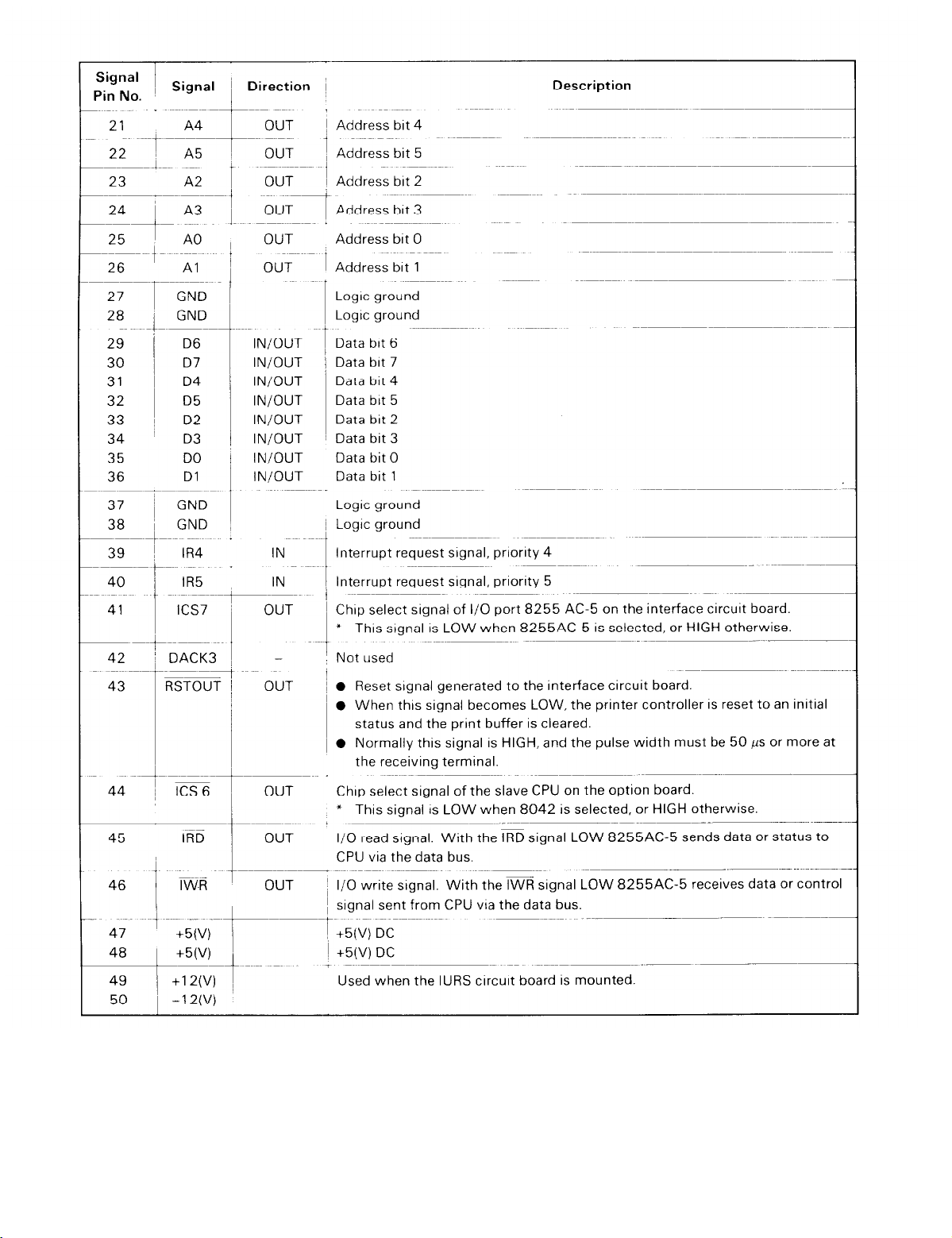
Note: “Direction” refers to the direction of signal as viewed from the UXMCL circuit board
Page 17
2) Table 2.2 CN2 pin assignment
(a)
Use . . . . . . . . . . . . . . . . . .
(b) Number of pins
.._.........................
Table 2.2 Pin assignment (CN2 of UXMCL)
Data exchange between the main circuit board UXMCL and the
driver circuit board UXDRV.
50
2-5
Page 18
2-6
Page 19
3) Table 2.3 CN3 pin assignment
(a) Use . . . .
(b) Number of pins
..__..................__....,,..._........._..
_,,.._.._.,,,.._._,,..r....__._
Table 2.3 Pin assignment (CN3 of UXMCL)
To supply power from the power supply board UXPS/PSU 24E to
the main circuit board UXMCL.
9
Note: “Direction” refers to the direction of signal as viewed from the UXMCL circuit board.
4) Table 2.4 CN4 pin assignment
(a) Use
,....,,...,.._...__.....__..._,.,,,_.,...._...._..
Signal exchange between the control panel on the UXMCL circuit
board.
(b) Number of pins _...,,...,,_,,,........._...... 8
Table 2.4 Pin assignment (CN4 of UXMCL)
Note: “Direction” refers to the direction of signal as viewed from the UXMCL circuit board.
2-7
Page 20
5) Table 2.5 CN5 pin assignment
(a) Use
___...__....__..._.._.._._..._.__.................
Exchange of head/home position signals between the printer me-
chanism Model-3660 and the main circuit board.
(b)
Number of pins
4
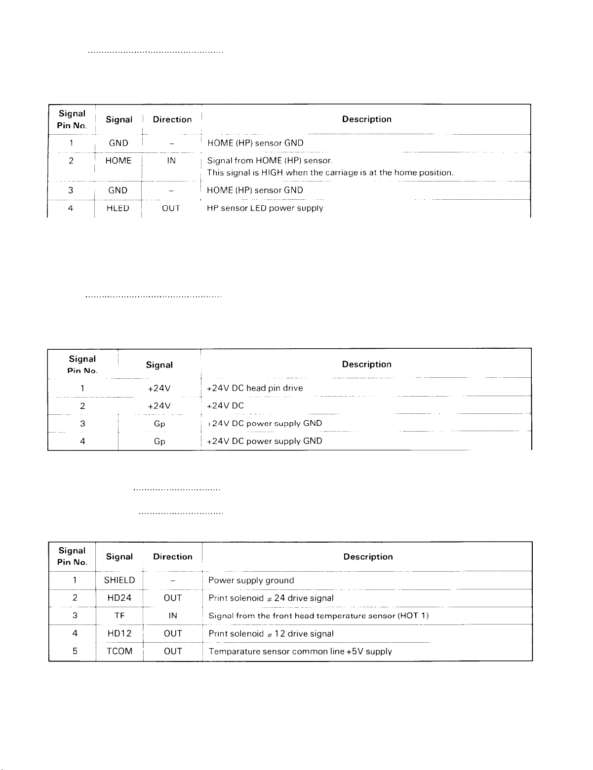
Table 2.5 Pin assignment (CN5 of UXMCL)
Note: “Direction” refers to the direction of signal as viewed from the UXMCL circuit board.
2.3.2 Connector on UXDRV circuit board
1) Table 2.6 CN1 pin assignment
(a) Use
(b)
._........_.......................................
Number of pins
To supply power from the power supply board UXPS/PSU 24E to
the driver circuit board UXDRV.
4
Table 2.6 Pin assignment (CN1 of UXDRV)
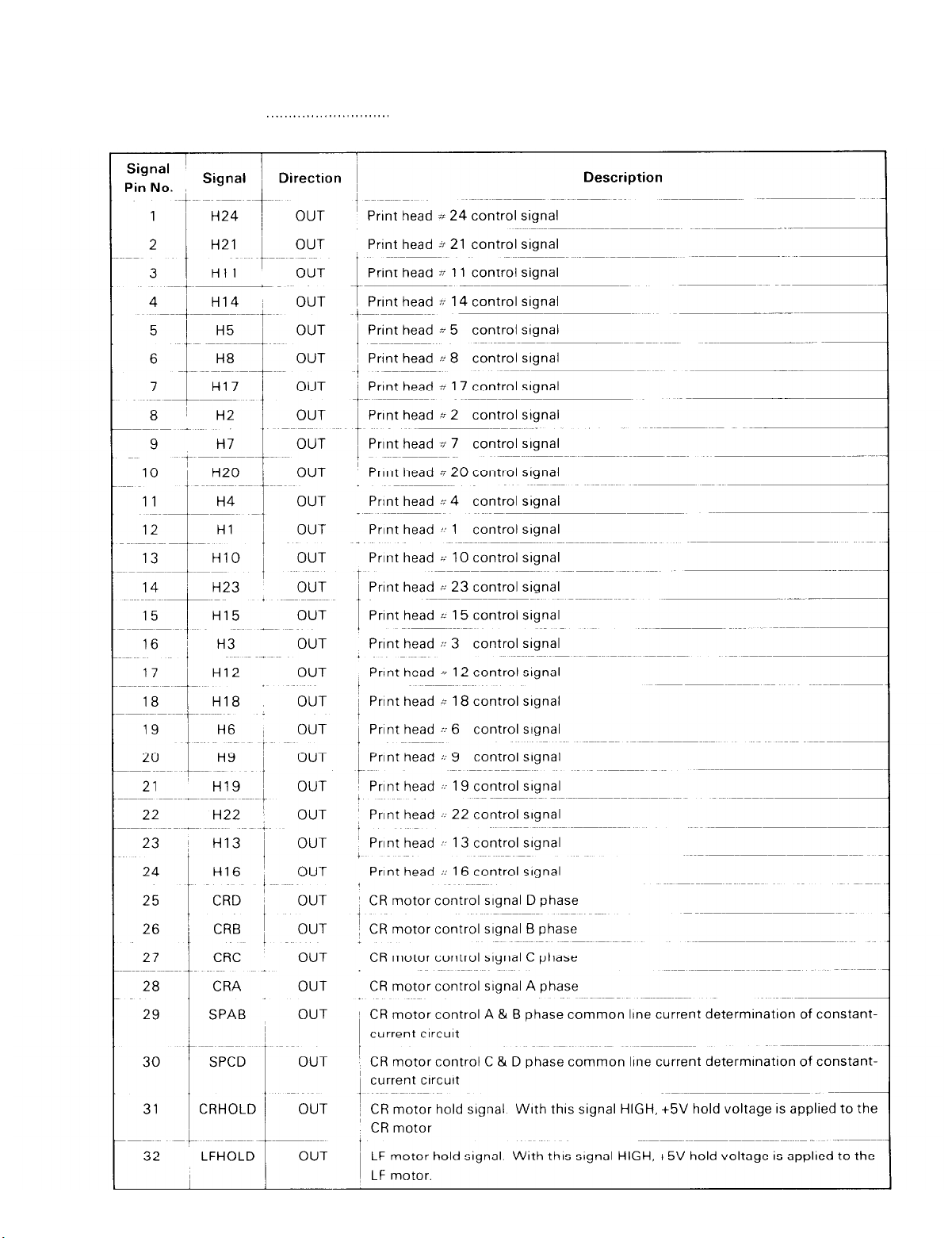
2) Table 2.7 CN2 pin assignment
(a)
Use
(b) Number of pins
.._.._._._...._._......_...._...
__..._._._.._.__..._......_....
Table 2.7 Pin assignment (CN2 of UXDRV)
Data exchange between the driver circuit board and the
Model-3660 printer mechanism.
34
2-8
Page 21
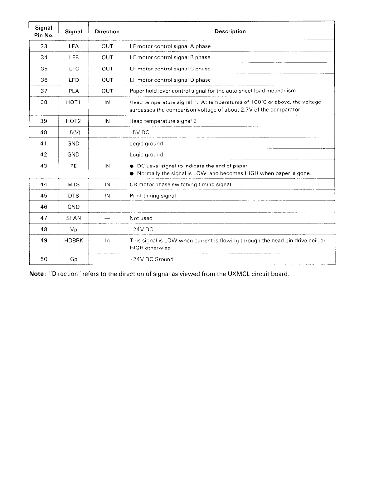
Note: “Direction” refers to the direction of signal as viewed from the UXDRV circuit board.
2-9
Page 22
3) CN3 pin assignment
Refer to Table 2.2.
4) Table 2.8 CN4 pin assignment
(a)
Use
Exchange of carriage motor signals between the drive circuit board
and the Model-3660 printer mechanism.
(b)
Number of pins .._............
18
Table 2.8 Pin assignment (CN4 of UXDRV)
Note: “Direction” refers to the direction of signal as viewed from the UXDRV circuit board
Page 23
5) Table 2.9 CN5 pin assignment
(a) Use.
(b) Number of pins
.,.,.,,,....,..,.........__......................
,._._........._...__...........
Table 2.9 Pin assignment (CN5 of UXDRV)
Exchange of control signals between the drive circuit board
and the Model-3660 printer mechanism for paper feed motor or
paper hold release plunger.
12
6) Table 2.10 CN6 pin assignment
(a)
Use . . . . . .._.._...................
(b)
Number of pins .._....................
Table 2.10 Pin assignment (CN6 of UXDRV)
7) Table 2.11 CN7 pin assignment
(a)
Use .._.._..._...................
(b) Number of pins
Table 2.11 Pin assignment (CN7 of UXDRV)
To supply power to the fan set UA from the driver circuit board.
2
onnectlon of the driver circuit board and the ceramic resistance
C
2
2-11
Page 24
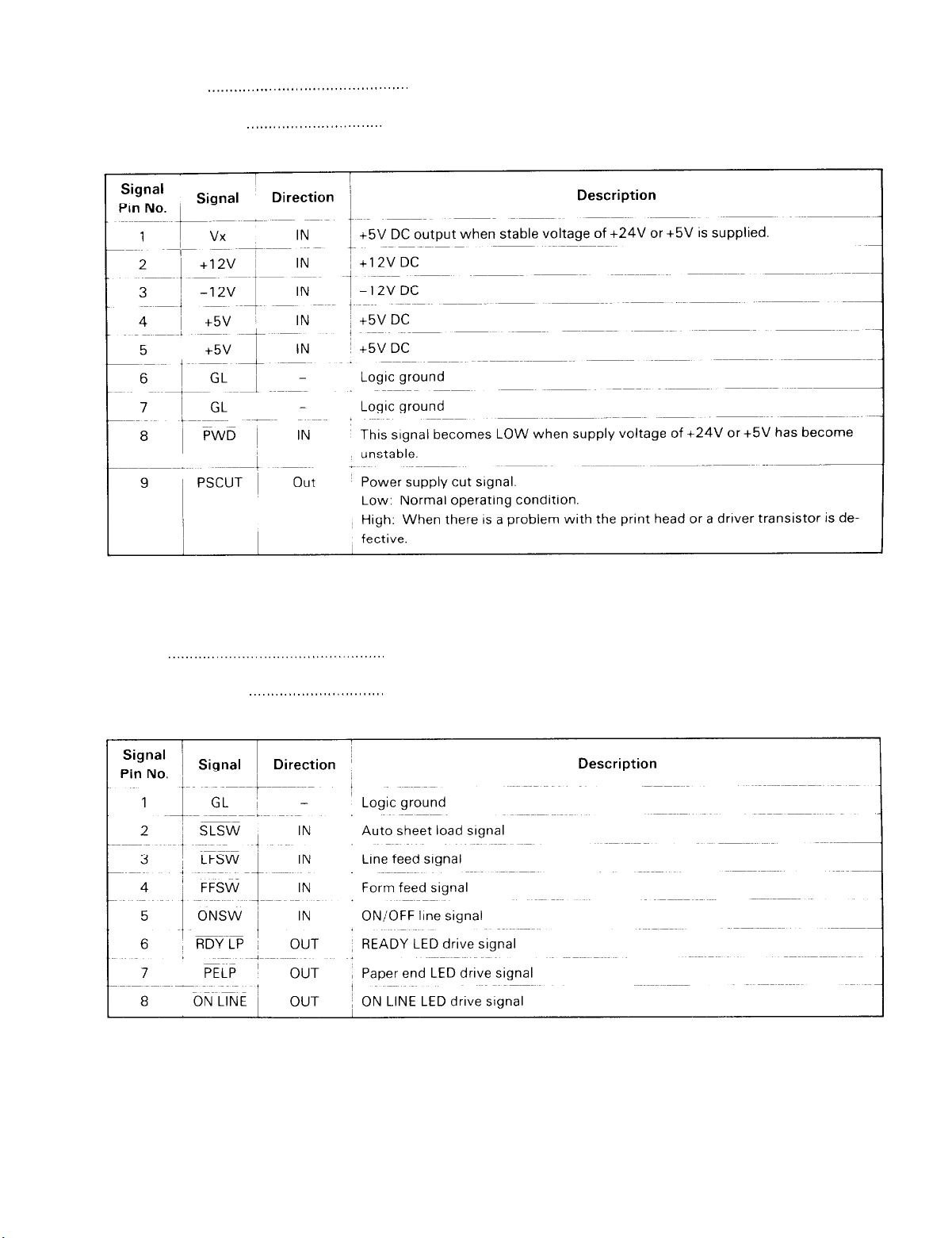
2.3.3 Connector on UXPS/PSU 24E circuit board
1) CN1 pin assignment
AC power is supplied from UXFIL circuit board
2) CN2 pin assignment
Refer to 2.3.1 3) Table 2.3
3) CN3 pin assignment
Refer to 2.3.2 1) Table 2.6
4) Table 2.12 CN4 pin assignment
(a) Use
____..__...,,.,.,..._.._..._._..,..._._..._...,_._
To supply power from the UXPS/PSU 24E circuit board to the fan
set UB.
(b) Number of pins
,.___._..__.,_,,._._..._.._....
2
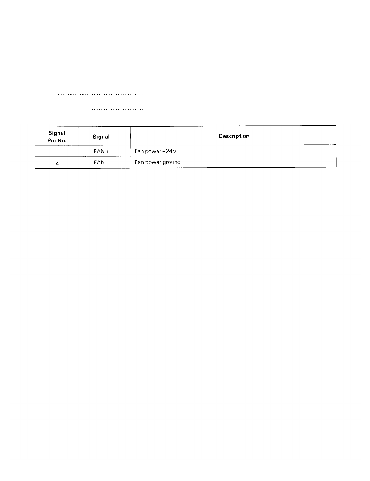
Table 2.12 Pin assignment (CN4 of UXPS/PSU 24E)
2-12
Page 25
2.4 Electrical Circuits
2.4.1 Power circuit
Overview
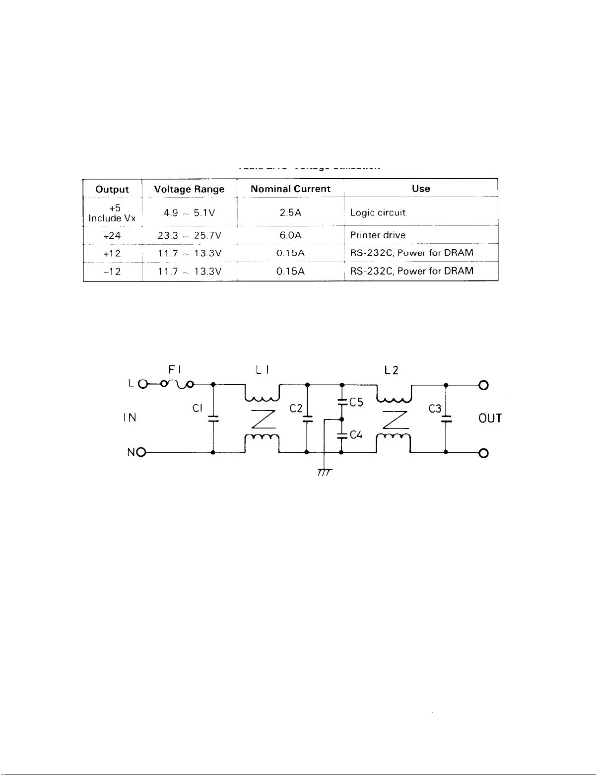
The power supply circuit of the LQ-1500 consists of a fuse and filter circuit and power supply circuit.
The output voltages are +5, +12 and -12V for logic circuits and +24V for printer drive.
The power supply circuit, employs a switching power supply system in which the input voltage is directly
rectified for use.
Table 2.13 Voltage utilization
[A] 100V/120V version circuit
1.
Norse filter circuit (100/120V version)
Fig. 2.3 Noise filter circuit
The noise filter circuit IS mounted on the UXFIL board together with the fuse. Incoming AC flows through
the power switch and fuse before being filtered by a noise suppression circuit on the UXFIL board. The
filter circuitry limits electrical interference both to and from the printer.
2-13
Page 26
2.
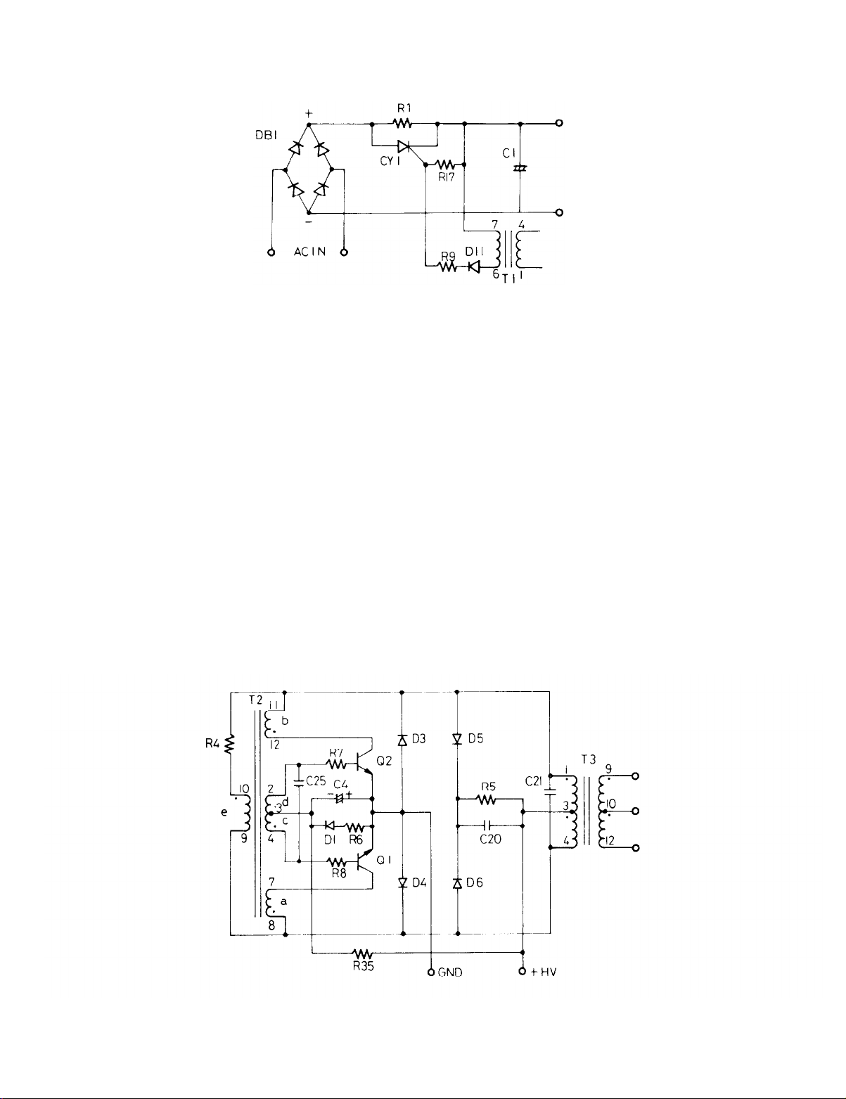
Rectifying circuit and inrush current prevention circuit
(100/120V version)
Fig. 2.4 Rectifying circuit and inrush current prevention circuit
In this power supply system, the AC input is directly rectified by the diode bridge DB1 and the output
voltages are as shown above.
An explosion-proof valve is provided in the upper part of the case of smoothing condenser Cl. If an abnormal voltage is applied to Cl, the explosion-proof valve will open, rendering the part inoperative.
In this power supply system, an inrush current flows at power on. Immediately after power on, when
Cl is not charged, an excessive charging current that may flow can cause the trouble of fuse F1 or
DB1. To prevent it, RI limits the inrush current. In other words, Cl is charged through RI at the time
of power on. With the start of power supply, a voltage is generated at the output of transformer T1,
and this is rectified by D11 and thyristor CY1 IS triggered. Now the thyristor shorts both the ends of
RI, thus completing the action of preventing Inrush current. The thyristor is conducting electricity as
long as the power supply is on.
When the thyristor does not conduct electricity because of some trouble, the power supply remains nor-
mal, but R1 gets heated abnormally. Also, RI may sometimes be disconnected when fuse F1 is blown.
3.
Converter circuit (100/120V version)
Fig. 2.5 Converter circuit
2-14
Page 27
In this circuit, transistors Ql and Q2 alternately supply current to the windings of transformer T3, producing AC voltage as the output. 50/60 Hz input is frequency converted into 20 kHz through the action of
pulse transformer T3. This circuit starts oscillating automatically at about 20 kHz by transformer T2. With
the power supply on, R35 causes the base current to flow and either Q1 or Q2 turns on. Once started, the
base current is supplied from windings a and b, so that the transistor, which has been off, turns on instantly. T2, which is a current transformer, is in a positive feedback connection. 1 /10 of the collector current
from windings c and d as the base current. Oscillation frequency is determind by the length of time it takes
the core of T2 to become magnetically saturated after excitation from windings a and b.
When this occurs, the transistor which has been of opposite polarity is generated at T3.
Winding e adds this voltage to the base current and thus prepares the transistor which has been off, to turn
on. Then oscillation continues, with the trigger voltage from winding e applied to Q1 and Q2 alternately.
R4 limits the current that flows to winding e.
The voltage drop caused by R6 and D1 is smoothed by C4 to produce an inverse bias voltage when Q1 or
Q2 turns off. D3 and D4 are used as the by-pass when part of the magnetic energy is returned to the input
power. D5 and D6 clamp the spike voltage generated by T3 at switching to the DC input voltage via R5
and C20.
The clamp voltage is about twice as large as the DC input voltage. C21 reduces the transitional switching
loss of Q1 and Q2. Q1 and Q2 are parts most liable to develop failure.
Note: When troubleshooting the power supply, Q1 and Q2 should be among the first check points. When
either of these transistors are isolated as a trouble source, both must be replaced. Replacing only
one of the transistors can result in continued problems.
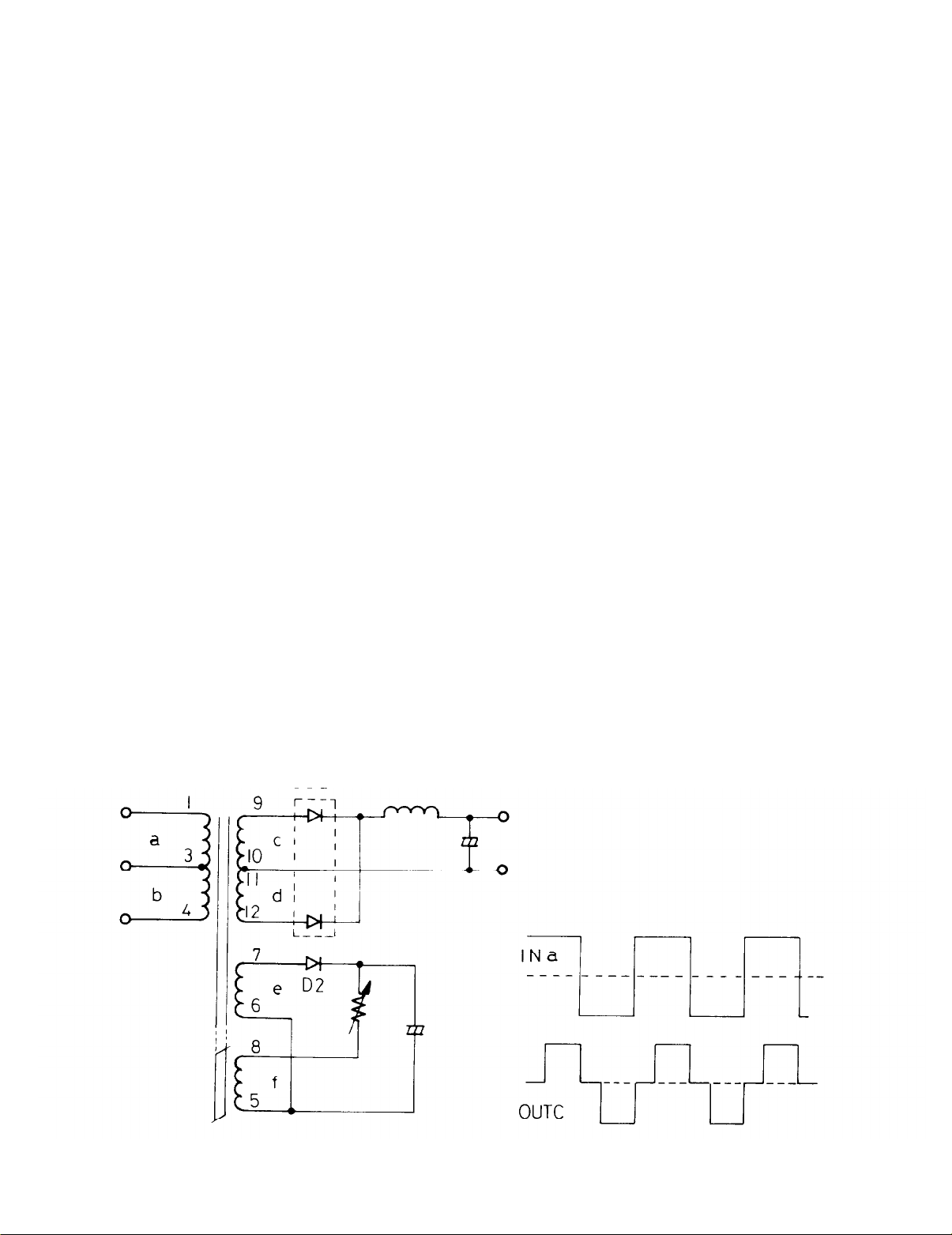
4. Power transformer circuit (100/120V version)
The variable leakage transformer not only performs power transformation by insulating the load from
higher voltage, but also stabilizes the output voltage by controlling the current flow to the control winding.
The VLT raises the DC output voltage by sending DC current into control winding f. From this current, the
VLT outputs a stabilized waveform.
With 20 kHz AC voltage applied to the input windings a and b, the pulse-width controlled AC voltage can
be obtained from the windings c and d. The winding e, which is an auxiliary power source of about 9V, is
used to drive the control winding f.
Fig. 2.6 Power transformer circuit
2-15
Page 28
5.
+24V output circuit (100/120V version)
Fig. 2.7 +24V output circuit
The +24V output circuit is capable of supplying an average current of 6A. In this circuit, the pulse-width
controlled voltage from VLT is rectified and smoothed. The output which is a pulse voltage, rectified by
DB2 is smoothed by choke coil T4 and C2, so a continuous load current flows.
T4, excited by the output voltage of DB2, stores magnetic energy. When the current stops flowing from
the VLT, T4 discharges the magentic energy, so the load current flows continuously.
C22 and R3 prevent the spike voltage from occurring as a result of rectification. L2 and C3 constitute a
spike prevention filter.
6. Output control circuit (100/120V version)
Fig. 2.8 Output control circuit
In this circuit, the output voltage is detected and the output is stabilized by controlling the current flowing
to the control winding f of VLT. The current to the control winding is supplied from e, which is the auxiliary
power source, and is driven by Q3 and Q7.
The output voltage is detected by zener diode ZD1 A constant output voltage is maintained which adjusts
the base current of Q7 as assuring a constant current flow to ZD1
If too much current flows to winding f as a result of machine malfunction, the system is short curcuited,
winding f is cut off and output drops below 12V.
R22 and C23 advance the phase so as to maintain a stable output voltage. L1 and C14 constitute and auxiliary power source smoothing filter.
2-16
Page 29
7.
Output cutoff circuit (100/120V version)
Fig. 2.9 Output cutoff circuit
The output cutoff circuit is activated when the PSC signal is input or 30V or more is output as a result of a
malfunction.
When the thyristor CY2 is kept on, Q13 turns on Q12 and stops the base current of Q3, so that power is
not supplied to the control winding of VLT. Then +24V output is shorted by triggering the thyristor CY3.
A PSC signal is output due to failure of a printhead drive transistor.
8. DC-DC converter (100/120V version)
C9-Cll
Fig. 2.10 DC-DC converter circuit
In this circuit, outputs of +5, +I 2 and -12V are produced from +24V.
This circuit starts oscillating automatically at power on.
As the base current flows through R31 and Q4 turns on. With winding c excited, an electromotive force is
generated in winding b. Q4 turns on quickly because positive feedback of the voltage in winding b is made
to the base current of Q4.
With Q4 switched on, the current flowing to winding c continues increasing until it is restricted by the base
current value.
Q4 is turned off quickly by a counterelectromotive force generated in winding b, when increase in collecter
current stops.
2-17
Page 30
The magnetic energy stored in transformer T5 during the ON period is discharged to the load side during
the OFF period. When the magnetic energy is discharged, the counterelectromotive force in winding b is
lost and Q4 starts turning on again. The output is stabilized by controlling the average current flowing to
the winding c.
As +5V output begins to rise, the current flowing into the winding c is reduced, and as it begins to drop, the
current flowing into the winding c is increased. These controls are performed with Q10 shunting the base
current flowing to Q4. The voltage detector TL1 adjusts the base current of Q10 to maintain the +5V output constant.
The oscillation frequency of the circuit lowers with more lead current or rises with less load current.
Under no load, the oscillation becomes intermittent. Normally the circuit operates at about 30 kHz.
D10 and C13 rectify and smooth the base voltage of Q4.
D13, which is a two-way zener diode, clamps the surge voltage generated by T5 to 68V to protect Q4.
VR1 is used to set the +5V output voltage.
9. +5V output circuit (100/120V version)
+5V output is used for the logic circuit.
The current flowing through DB3 charges C9 through 11. The extremely large current value, however
causes a large output voltage ripple which is smoothed by Ls and C12.
10. 12V output circuit (100/120V version)
12V output, which is not stable, is used by RS-232C.
Since the DC-DC converter stabilizes the output by detecting +5V, the output voltage drops to about 5V
when +5V is under no load.
11. Vx. PWD circuit (100/120V version)
Fig. 2.11 Vx. PWD
Vx is output when +5V and +24V voltages become stabilized and is used to prevent the misoperation of the
printer when the power supply is turned on or off.
+5V make from +24V, retains the stable condition longer than +24V. Therefore, Vx is output when the
+24V output is +21 V or above.
A voltage drop on the +24V line due to a power failure or machine malfunction turns Q11 on and triggers
the PWD signal. When PWD is output the CPU is reset and the printer is stopped.
2-18
Page 31

[B] 220/24OV version circuit
1. Noise filter circuit (220/24OV version)
Fig. 2.12 Noise filter circuit
A switching regulator generates noise because of its circuit configuration. Each country
has its own noise
regulations, the circuit configuration, Fig. 2.12, is adopted to meet VDE 0871 class B.
2. Rectifying circuit, inrush current prevention circuit and converter circuit (220/24OV version)
Fig. 2.13 Rectifying and converter circuit
The supply voltage passed through the noise filter circuit is rectified at D101 and smoothed at Cl06 and
Cl 07, providing the mid-point voltage as shown in Fig. 2.13.
R101 and SCR101 form an inrush current prevention circuit. When power is applied, the current is
charged to C106 and C107 via R101 with SCR101 OFF. When the charged voltage rises, the converter
oscillates, SCR101 turns ON and the current path changes from R101 to SCR101 Switching transistors
Tr101 and Tr102 form a symmetric excitation half-bridge type converter which is activated by T101. The
oscillation frequency depends on the saturation of T101. This converter supplies a symmetric pulse voltage to the transformer.
2-19
Page 32

3. Power transformer circuit (220/24OV version)
Fig. 2.14 Power transformer circuit
The transformer
T102,
a variable leakage transformer, has a construction capable of output control.
The pulse voltage input to the primary winding (terminals 1 and 4) is controlled by the DC current flowing
at the control winding (terminals 5 and 8) and is output to the secondary winding (terminals 9 - 12).
As shown in Fig. 2.16, the width of the pulse output to the secondary winding increases as the control current is made larger.
2-20
Page 33

Fig.2.16 Switching regulator circuit
This circuit is formed by a chopper circuit with a power supply of +24V.
As shown in Fig.2.16. when transistor Tr301 turns ON, collector current ic flows, supplying current to the
load.
At the same time, magnetic energy IS being stored in choke coil L (See Ton, Fig. 2.16). If transistor Tr301
turns off, collector current is also cut off. When this occurs, choke coil L maintarns current flow by emitting
the stored magnetic energy In the form of current, supplying the load and flywheel diode D.
Output voltage, Vout, is maintained at a constant level by a control IC, which constantly monitors output,
and switches transistor Tr301 on or off, as required to maintain a constant output.
The relationship between the input and output voltage is expressed as:
T
=-
ON
x Vin
Vout
T
5.
Vx, PWD (Power down) circuit (220/24OV version)
Fig.2.17 Vx, PWD circuit
This circuit compares the
+24V
output with the reference voltage to generate Vx.
The +24V output is divided by R402 and R403. Then, the devided voltage is compared with the reference
voltage obtained by ZD401. When it exceeds 2OV, TR402 turns ON and sends 5V to pin Vx. At
the same time, open collector transistor TR403 turns ON.
This circuit has a slight hysteresis to prevent chattering due to ON/OFF operation.
2-21
Page 34

2.4.2 Reset circuit( Fig. 2.18)
The reset signal is used to reset and start the CPU, causing It to initiate the routine which initializes the processor and associated circuitry.
The reset signal is output only in the following cases:
I) At power on: The signal is output for about 30 ms at the turning on of power.
2) By interface signal: The signal is given while the INIT signal is output from the host computer.
Fig. 2.18 Reset circuit
The reset signal is output at power on when Vx (+5V) is applied to the power on reset circuit, consisting of
RM9, R3 and C4; it is passed on to IC 9B, pin 1, 8B and 8A, which IS the reset signal port initiator.
Time constant of the reset pulse is applied at R69 and C4.
This time constant is approximately 30 ms.
Upon the input of an INIT signal from the interface board, the interface reset (INIT) signal is input to: the
main CPU Z-80A; slave CPUs 8042 and 8041, PPI 8255AC-5; gate array uPB6101-009; and timer
NE555. The INIT signal is output only during the system reset or I/O reset of the host computer that controls the LQ-1500.
If power is off the reset cannot be output.
2.4.3 Sensor circuit
Five sensor circuits (HP, MTS, DTS, PE and HOT1 and 2) monitor status of the printer mechanism and inform the Z80-A CPU as to the mechanism’s operational status at any given time.
1)
Home position sensor circuit (Fig.2.1 9)
Fig. 2.19 HP sensor circuit
Page 35

The home position sensor circuit detects signals defining when the printhead is in or out of the home position. The signal is read when the power switch is turned on or signal INIT is applied to the printer. This circuit also operates at the instruction of carriage return.
When the carrage is out of the home position, phototransistor turns on causing a HIGH output signal to be
emitted to the CPU. At the return of the carriage to the home position, the photocoupler is screened, the
phototransistor is turned off, and the output of HP drops to LOW. The carriage is in the home position, and
it is notified to the 8042. The output signal from the phototransistor is integrated and input to the Schmitt
circuit, which prevents the waveform of the output signal from being disturbed by noise or mechanical vi-
tion.
bra
MTS sensor circuit
2)
Fig. 2.20 MTS sensor circuit
The MTS sensor circuit detects the signal that defines the speed of the head carriage. When the light is
screened by the slit plate (Fig. 2.21) at the photocoupler, the photodiode turns off and HIGH level voltage is
applied to the transistor base of the sensor so that the transistor turns on. As a result, the MTS signal be-
comes LOW. When the light passes through the slit, the photodiode turns on and the transistor of the sensor turns off, so that the MTS signal becomes HIGH.
The period of MTS signal is 860s in the draft mode and 2.52 ms in the letter quality (LQ) mode.
Fig. 2.21 Sensor assembly
2-23
Page 36

3) DTS sensor circuit (Fig.2.22)
Fig. 2.22 DTS sensor circuit
The DTS sensor circuit detects the print timing signal. This signal comes in three pulses in one period of
MTS. As shown in Fig. 2.22, it operates the same way as the MTS sensor circuit.
The timing of DTS signal is 287s in the draft mode and 840s in the letter quality (LQ) mode.
Fig. 2.23 PE sensor circuit
The paper end sensor circuit employs a magnet-electricity conversion system using a Hall IC; output is of
the open collector type. The output signal from the sensor is integrated once and input to the Schmitt circuit, which prevents the waveform of the output signal from being disturbed by noise or mechanical vibration.
When paper has been inserted in the mechanism, the Hall IC is off and pulled up by R63, so that the output
of PE signal is LOW. When the paper is gone, the Hall IC goes on and the collector drops to ground level,
so that the output of PE signal becmes HIGH. The PE signal is applied to T1 (pin 39) of CPU8041 A. It is
possible to render the PE signal Ineffective via a control code or DIP switch setting.
The RE sensor will be ignored and the error signal will not function when DIP switch 2-2 is set or an ESC 8
control code is input. In this mode of operation, although the PE LED goes on, the READY LED remains on
and data can still be received.
* See the operating manual for an explanation of DIP switch settings and use of control codes.
2-24
Page 37

5) Head temperature sensor circuit (Fig. 2.24)
Overheating of the print head during heavy duty printing operation is prevented by the head temperature
sensor circuit.
Fig. 2.24
Head temperature sensor circuit
The head temperature sensor circuit detects the temperature of the print head unit
A fan, situated at home position circulates air, providing a cooling system.
As the temperature of the print head unit reaches approximately 100°C or above, the printing is halted temporarily and the print head unit IS returned to the home position.
A thermistor provided in the print head unit is pulled up to 5V. As the temperature of the unit rises, the resistance decreases and the voltage at the negative terminal (HOT1, HOT2) of the comparator rises higher
than the positive terminal of the comparison voltage.
As the output terminal becomes LOW, Q3 switches from on to off, and the collector level moves from LOW
to HIGH.
2-25
Page 38

2.4.4 Carriage motor control circuit (Figs. 2.25.26)
The control signal of the carriage motor is output from 8042 of the main circuit board. The signal is first
received by the transistor array and then driven by the regulator IC STK6982 (IC2).
The 2-2 phase carriage motor runs in combinations of phases A to D. (See Table 2.14 and Fig. 2.25.)
Fig. 2.25 Motor circuit
The belt, motor sequence for driving the timing belt is shown below.
2-26
Page 39

Fig. 2.26 CR motor drive circuit
2-27
Page 40

The phase changing signal for the carriage motor is output from P20 and P21 of CPU 8042. The control
signal of phases A and B is inverted via the phase inverter, 1 1 C, and used as the control signal of phase C
and phase D, respectively.
Power supply to the carriage motor is monitored by resistances RI and R2 connected to the EAB and ECD
terminals of STK6982, and the outputs of CAB and CCD are controlled in accordance with the reference
voltages S12 and S34 of the comparator inside STK6982. Accordingly, the speed of the carriage motor
can be changed by changing this reference voltage; reference voltage changes depending on whether the
resistances R42 and R43 or R44 and R45, connected to the transistor array by the output of P23 and
P24
of 8042, are selected. Also, ZD4 is provided to prevent counterelectromotive force. Power supply to the
motor is such that switching to high speed can be made by STK6982. The electric energy stored in each
coil is discharged following the end of power supply there, which can cause the breakdown or malfunction
of the elements. To prevent It, the energy produced by the counterelectromotive force is released through
the zener diode.
When the output of P22 of 8042 is HIGH, the HOLD terminal of STK6982 is HIGH. Therefore the common
line is cut off from 24V power supply and, instead, the power is supplied from Vp via the cement resistances D32 and D33. And the current flows through all the phases simultaneously, thus putting the carriage motor in a HOLD state.
Control method:
The Model-3660 carriage drive motor can be stopped at any position by controlling acceleration/
deceleration and the alternation of print direction.
A closed loop control method is used in which the MTS timing signal is fed back to the pulse motor drive
phase switching.
Closed loop control:
The motor phase switching is made by comparing the MTS output from the printer to the control time setting.
When the MTS period, compared with the time setting, IS longer, the CR motor phase switching is made at
the leading edge of MTS. (See Fig. 2.27.)
When the MTS time setting is shorter, MTS is output within the time setting, though the CR motor phase
switching is not made at this time, but after the lapse of the time setting. (See Fig. 2.27.)
2-28
Page 41

(1) Motor bias voltage
The bias voltage for the motor is of two kinds; one for operation use and the other for non-operation use.
Table 2.15 Motor bias voltage
(2) Carriage motor drive signal timing
(a) Acceleration control and constant speed control
For acceleration control and contant speed control, the following time settings (Table 2.16) are available in
the printing speed
(CR
motor speed) modes of1163 pps, 769 pps, 592 pps and 397 pps:
Table 2.16 Speed control table
2-29
Page 42

Table 2.17 Data of decelerate time
Page 43

Fig. 2.29 Deceleration and stop at home position (In case of 1163,769 pps)
Page 44

Fig. 2.30 Acceleration and printing control from position other than home position
Fig. 2.31 Deceleration and stop at home position (In case of 1163, 769 pps)
Page 45

(c) Home Position Seek
Movement of the carriage to home position at printer power on is called the home position (HP) seek.
The CR motor speeds during the home position seek are all in the 1163 pps mode. The following flow
chart exemplifies sequence of HP operational events.
Fig. 2.32 Flow chart of home position seek
2-33
Page 46

(d) Acceleration and printing control from home position:
@
By the control of a) and b) of 12), the carriage is moved from left to right (column 1 to column 80).
In this case, reading to recognize the HP signal is done only in the excitation condition memorized
in v) of d). Accordingly the HP signal read timing is every four MTSs.
@
The print occurs during MTS and thereafter following the MTS where the HIGH of the HP signal is
recognized. The printing occurs during maximum of MTS 816 pulses (DTS2448 pulses).
(e)
Deceleration stop at positions other than home position:
Deceleration control is started from the next MTS (Tm + 1 = T) after the printing of the last dot on the
line (MTS immediately after this if Tm). It is stopped after 18 times of phase switching.
(f)
Acceleration and printing control from positions other than home position:
@
By the control of a) and b) of 12), the carriage is moved in a chosen direction.
@
The printing area is the 19th MTS (TN) and thereafter.
(g) Deceleration and stop at home position
The HP signal is recognized at every MTS during the shift of the carriage from right to left (column 136
to column 1 ), deceleration is started from the next MTS (TM + 1) of the MTS (TM) where the change of
HIGH to LOW of HP signal is recognized, and the CR motor is stopped after 18 phase switches.
(h) Setting of speed control terminals
In each control mode the terminals of 8042 (P23 and P24) in the Fig. 2.26 must be set as follows:
Table 2.18
2.4.5 LF motor control circuit (Fig. 2.34)
The control signal of the 4-phase excitation LF motor (Fig. 2.33) is output from CPU 8041 A on the main
circuit board. This signal is sent to IA to ID inputs of the transistor array HA1 3007. With the input at HIGH
Level, the inside transistor turns on, forming a closed circuit of power supply (+24V): LF motor, diode,
HA1 3007, GND, and the current flows through the coil of the LF motor. The LF motor is thus driven with
the voltage-applied phase switched by turning the transistor on and off inside HA1 3007 by the input signal IA to ID.
The operation mode or the non-operation mode can be selected by the output of P27 of CPU 8041 A.
With this output at HIGH, transistor 029 is off and +5V is supplied to LFCOM via resistance R4 and diode
D31, putting the LF motor in the non-operation mode. With the output of P27 at LOW, on the other hand,
transistor Q29 is on and Vp (+24V) is supplied to LFCOM via D30, putting the LF motor in the operation
mode.
Basically, the belt motor is driven by the 2-2 phase excitation system
Fig. 2.33 LF motor circuit
2-34
Page 47

Fig. 2.34 LF motor drive circuit
(1 ) Motor bias voltage
The bias voltage for the motor is of two types. One for operation use and the other for non-operation use
Table 2.20 Motor bias voltage
(2) Paper feed step motor driven signal timing
Fig. 2.31 shows the time chart for control of the paper feed step motor. The control method is a ramp-up
and ramp-down control. The time settings for this control are as shown in Table 2.21.
This control, however, is not performed when the amount of paper feed is five steps or less. The time set-
ting at this time is constant speed drive of 4.2 ms per step.
(4) Paper feed time
3.3 ms/0.l41 mm
100 ms/4.23 mm (with continuous paper feed)
2-35
Page 48

Fig. 2.35 Paper feed timing chart (In case of N pulse paper feed, N > 5)
Page 49

2.4.6 Head driver circuit (Fig. 2.36)
(1 ) Solenoid driving control
The head has 24 coils and +24V is always supplied to one end of each of the coils. To effect printing with
the coils powered, it is necessary to switch on the driver transistors Q1 to Q24 and bring the voltage at
one end of the relevant COils to the GND (Fig. 2.32).
A sample sequence is as follows.
Print data put on the data bus are output to each port by a total of five control signals, namely, the A0 and
Al signals from the main CPU Z80A, the control signal from Z80A, the RD and WR signals from the gate
array uPB6101-009, producing various timing signals used inside the LQ-1 500, and the chip select signal
from the decoder LS138. The output data is input to the transistor array and produces an open collector
output and is pulled up to Vx by the block resistance RM1 and RM2.
With the port output of 8255AC-5 going LOW, the out terminal of µPA79C is internally disconnected from
the ground and assumes an Open state.
With the port output of 8255AC5 HIGH, the output terminal of µPA79C is internally connected to ground.
The driving pulse width is determined by the output of pin 1 1 of IC 10C. When this output is LOW, Q1 is
on and the power supply Vx is applied to the base as a pulse to turn on Vcc of uPS79C and the driven transistor through Q1. Thus the power is supplied to the solenoid and the head pin is driven.
After the lapse of driving time, as shown in Fig. 2.32, the output of pin 11 of IC 10C goes HIGH, Q1 turns
off and the supply of Vx stops. The driver transistor 2SD1 392 then turns off to stop the solenoid drive.
When the output of pin 1 1 of 10C 1 0C goes HIGH, the output of pin 8 goes HIGH simultaneously and by turn-
rng 04 on, the base charge of the driver transistor is released to the ground through block resistances
RM1,
RM2,
R2 and Q4. This realizes a high-speed switching of the driver transistor.
Voltage applied to print head (VDC)
Fig. 2.36 Applied head voltage and driving time
2-37
Page 50

(2) Counterelectromotive force absorbing circuit
As the power supply to the solenoid is switched on and off at high speed, counterelectromotive force is
produced in the coil. So that the driver transistor is not adversely affected, a diode and a diode array are
provided to each driver transistor (points A, B), and a transistor, resistance, zener diode and electrolytic capacitor (D19, Q27, R6, ZD3, C7) are provided for every 8 driver transisters by wired OR as shown in Fig.
2.37.
As the counterelectromotive force becomes about 44V at point D in the figure, the current flows into the
base of Q27 through R6 and ZD3. Then 027 turns on and the voltage beyond it is fed back to the power
supply Vp via 027.
(3) Protective Circuit
The Voltage at point C in Fig. 2.37 IS at GND level during the solenoid drive and +24V during the non-drive
period. Because of the zener diode ZD3 provided, the current does not flow through the zener diode during
the drive. And the output of pin 15 of 15C becomes open and is pulled up to +5V by R23. During the non-
drive time, the current flows through the zener diode and the output terminal of pin 15 of 15C is internally
connected with ground. The output of pin 2 of 14C on the other hand is internally connected to ground
during the drive sequence and is pulled up to +5V during the non-drive period.
The output of pin 15 of IC 15C and the output of pin 2 of 14C are in wired CR. Consequently, as long as a
normal power is supplied to the solenoid, point E in Fig. 2.37 is always connected to ground. Because voltage Vx is applied to the base of Q2, Q2 remains OFF.
However, if power is continuously supplied due to failure of the driver transistor, point E in Fig. 2.37 goes
HIGH and the base of Q2 lowers to GND. Hence, Q2 turns on, Vx is sent as PSCUT to the power supply circuit, and the power supply circuit, receiving this signal, stops the power supply.
Fig. 2.37 Head driver circuit
Page 51

(4) Driver circuit waveform
Fig. 2.38 Driver current waveform
2.4.7 Auto sheet load circuit
The auto sheet load circuit sets the paper when the sheet load switch is pressed. The operation consists of
the control of the paper hold release lever and the control of the paper feed motor. Refer to 2.4.5 for the
control of the paper feed motor. The CPU 8041 (12D) first checks the OFF-LINE condition when sheet load
switch on the control panel is pressed. Then, if the printer is OFF-LINE, the 8041 determines wheather
paper is set in position. When paper is present, the output of P21 of 8041 goes LOW and the output of pin
10 of IC 15C goes off. Since it is pulled up to 5V by R19, Q30 turns on, the solenoid is driven, and the paper hold lever is released.
In this state, the PF motor is driven at 510 pulses to execute paper feeding. On completion of paper feed,
CPU 8041 brings P21 to high level. Since pin 10 of IC 15C is internally connected to ground, Q30 turns
off, and the base lowers to ground. The solenoid drive is stopped and the paper hold lever turns to the original position. By this control the printing start position is set to about 21 mm from the paper end (print
position of head wire 12). And it is about 19.5 mm at the top of character
Fig. 2.39 Auto sheet load circuit
2-39
Page 52

2.4.8 Other function
Logical seeking (Fig. 2.40)
The logical seeking maximizes operation speed of the bidirectional printer. It does away with the necessity
to start printing from the left end (home position) after each line of printing, but permits printing from any
position after a line feed. Fig. 2.40 shows the sequences of logical seeking.
(a)
When the power switch is turned on, the head carriage, regardless of its position, returns to the left
end, home position in an action of @ to
(b)
Upon receiving print data “EPSON” for a line, the printing is performed in an action of @ to @ with
the head carriage moving to
(c)
The CPU, receiving the next data, analyzes It and determines the acceleration start position of the car-
positior! @.
0.
riage.
(d)
In an action of @ to 0, the carriage is moved to position
@).
Then it goes through acceleration,
printing and deceleration.
(e)
In an action of @ to 0, acceleration and printing are performed. Then the carriage returns to the
home position because in this case the stop position is considered equivalent to the reset position.
Fig. 2.40 Logical seeking
Page 53

2.5 Printer Mechanism (Model-3660)
The Model-3660 printer mechanism features a 24-pin print head and incorporates all of the sophisticated
technology of previously produced EPSON printers.
Operation of the 24-pin print head is supported by the carnage components, including the timing belt, ribbon driving gears, and the carnage motor; the paper feed mechanism, including the platen sprocket assemblies and paper feed motor; and the sensors, which communicate the disposition of the print head and
the paper supply at any given time. The printer mechanism is illustrated in Fig. 2.41.
Fig. 2.41 Appearance of the printer
2.5.1 Operation
2.5.1 1 Sensor mechanism (Signal generating mechanism of Model-3660)
The sensor mechanism is composed of an HP (home positron) sensor, an MTS/DTS sensor, a PE (paper
end) sensor and a print head temperature sensor.
l
The purpose of the HP sensor is to determine the home position of the carriage. The sensor generates
a reference signal for the printing position.
0
The MTS/DTS sensor detects the carnage speed and print timing.
0
The PE sensor detects the presence or absence of paper.
0
The print head temperature sensor detects the internal temperature of the print head. The sensor out-
puts a signal when the print head reaches temperature levels which could damage components.
2-41
Page 54

1) HP (home position) sensor
The HP sensor consists of an HP sensor board and a sensor plate located at the bottom of carriage.
While the sensor plate intercepts the optical axis of the photocoupler, a HIGH signal is emitted (open
collector output).
2) MTS/DTS sensor (print timing signal sensor)
The MTS/DTS sensor consists of an MTS/DTS sensor board and a sensor plate located on the car-
riage motor shaft. When the slit of the sensor plate comes to the predetermined position, an LOW
signal is given (open collector output).
Fig. 2.42 MTS/DTS sensor
3) PE (paper end) sensor
The PE sensor consists of a Hall IC mounted on the PE sensor board and a permanent magnet
mounted on the PE sensor lever. When the printer is out of paper, the magnet touches the Hall IC
and generate a signal.
4) Print head temperature sensor
Two thermistors are built into the print head to detect excessive temperature gains. Their resistance
value aids in maintaining component compatible operating temperatures.
2.5.1.2 Print head assembly
The print head unit mounted on the carriage is moved right and left on the carriage shafts A and B by
the operation of the timing belt. This belt is driven by the timing belt motor assembly through the belt
driving pulley and belt driven pulley.
1) Carriage assembly (Fig. 2.43)
The carriage assembly is moved by the timing belt which is driven by the four phase carriage motor.
Each motor phase produces a movement of the carriage. As the timing belt motor runs, the DTS sig-
nal is generated, and current is also fed through the head driving coil, causing the dot wires to fire.
2-42
Page 55

Fig. 2.43 Carriage mechanism
2) Operation of print head unit (Fig. 2.44)
The movement of a dot wire in printing a dot is as follows:
@
With the current flowing through the head driving coil, the actuator plate is attracted to the iron
core. At this time, the dot wire, which is engaged with the actuator plate, flies out against the
platen assembly.
@
The dot wire thus pushed out strikes at the platen assembly and prints a dot on the paper
through the ribbon
@
On completion of the supply of current to the head driving coil, the actuator plate is caused to re-
turn to its original posltion by the action of the spring. By the impact energy and the force of the
wire return spring, the dot wire is brought back to the original position to engage with the actuator plate and held in readiness.
Fig. 2.44 Print mechanism
2-43
Page 56

3) Correspondence between dot wires and FPC terminals
Fig. 2.45 Printhead connector
2-44
Page 57

2.5.1.3 Paper feeding mechanism
The paper feeding mechanism of the printer comprises two systems: a friction feed system to be used for
cut sheet and a tractor feed system to be used for continuous business form 4 - 16 inches in width.
Each of the two systems have functions such as ordinary feeding and quick feeding. The printer is also
equipped with an auto loading mechanism for setting cut sheet automatically for printing.
1 ) Friction feed system (for cut sheet) (Fig. 2.47)
The paper is held between the platen, the paper feeding rollers and the paper holding rollers. When
the pulse motor rotates, the gears constituting a paper feeding gear train are driven in the directions
of arrows, respectively. Consequently, the paper is frictionally fed by the platen, paper holding
rollers and paper feeding rollers in the direction of the arrow. The paper holding rollers and paper
feeding rollers are pressing the paper against the platen by the action of springs.
The paper can be set free by operating the release lever.
Fig. 2.46 Friction feed mechanism
2-45
Page 58

2) Tractor feed system (for continuous business from 4 - 16 inches in width)
The paper is held on sprocket wheels, some of the sprocket pins being engaged in holes in the paper.
When the pulse motor rotates, the gears in the paper feeding gear train are driven in the directions
of arrows, respectively. Consequently, the paper is driven by the sprocket wheels in the
direction of the arrow.
When the tractor feed system is used, the paper feeding rollers are held apart from the platen by
the action of the release lever.
Fig. 2.47 Tractor (sprocket) feed mechanism
2-46
Page 59

3) Auto loading mechanism
Set a cut sheet between the platen and the paper feeding lever. When the release solenoid is energized, the solenoid shaft, sub paper holding lever and paper holding lever move in the direction of
the arrow respectively to disengage the paper holding roller from the platen. At this point, the pulse
motor (for paper feeding) is driven to feed the paper as specified. When the release solenoid is deenergized, the solenoid shaft, sub paper holding lever and paper holding lever return to their original
positions respectively, causing the cut sheet to be pressed against the platen and set for printing.
Fig. 2.48 Auto loading mechanism
2-47
Page 60

2.5.1.4 Ribbon feeding mechanism (Fig. 2.49)
The ribbon unit consists of a cassette ribbon and a ribbon feeding mechanism. The ribbon feeding me-
chanism is set at the bottom of the carriage.
When the carriage moves to right or left, the ribbon driving pulley is turned by the ribbon driving wire
wound around it so that the ribbon driving gear always turns counterclockwise in the next gear train.
The inked ribbon is housed in the cassette case in an endless state. The inked ribbon between the ribbon
feeding roller and the ribbon pressure roller is fed when the ribbon feeding roller set in the ribbon driving
gear is turned.
A ribbon braking spring is provided at the exit of the cassette case for preventing the ribbon from losing
tension, and a ribbon mask IS provided for protecting the paper from being stained by the inked ribbon.
Fig. 2.49 Ribbon feed mechanism
2-48
Page 61

CHAPTER 3
OPTIONAL EQUIPMENT
Centronics Compatible
3.1
3.1 .1
Overview..
3.1 .2 Specification..
3.1 .3 Operating
3.1 .4 Block diagram..
3.1.5 Circuit diagram..
3.1 .6 Component
RS-232C/Current
3.2
3.2.1 Introduction
3.2.2 Specification..
3.2.3 Operating
3.2.4 Block
3.2.5 Circuit diagram..
3.2.6 Component
IEEE-488
3.3
3.3.1 Introduction
3.3.2 Specification..
diagram..
Interface..
Parallel
...................................................................................
.............................................................................
principal
...........................................................................
.........................................................................
layout..
Interface
Loop
................................................................................
.............................................................................
principal
...........................................................................
.........................................................................
layout..
.............................................................................
................................................................................ 3-22
.............................................................................
interface . . . . . . . . . . . . . . . . . . . . . . . . . . . . . . . . . . . . . . . . .
....................................................................
....................................................................
.......................................................
....................................................................
....................................................................
3-1
3-1
3-1
3-4
3-6
3-7
3-8
3-9
3-9
3-9
3-15
3-19
3-20
3-21
3-22
3-22
3.3.3 IEEE-488 operational parameters..
3.3.4 IEEE-488 functional commands..
3.3.5 Block diagram..
3.3.6 Circuit diagram
3.3.7 Component layout..
3.4 Single Bin Cut Sheet Feeder (# 8334).
Double Bin Cut Sheet Feeder (# 8344)
3.4.1 Introduction
3.4.2 Specification
3.4.3 Principle of operation..
3.4.4 Disassembly and assembly,
3.4.5 Troubleshooting
3.4.6 Preventive maintenance
...........................................................................
...........................................................................
....................................................................
...
.............................................................................
...............................................................................
..............................................................
..................................................... 3-42
.........................................................................
...........................................................
..........................................
............................................. 3-27
..............................................
3-26
3-29
3-31
3-32
3-33
3-33
3-34
3-36
3-52
3-60
Page 62

3.1 Centronics Compatible Parallel Interface Unit (Cat. No. 7171)
3.1 1 Overview
With the IUPIF interface board, a centronics parallel data from a host computer can be output to and painted dot by the EPSON LQ-1500 terminal printer.
3.1.2 Specification
3.1.2.1 Interface
(1) Data Transmission
(2) Synchronization
(3) Handshaking
(4) Logic level
3.1.2.2 Condition setting on the interface board
These are two DIP switches on the centronics parallel interface board. These switches are set as follows:
(1) DIP switch setting
A. DIP 1
: 8-bit parallel
: Externally supplied STROBE pulses
: ACKNLG or BUSY
: Input data and all interface control signals are TTL compatible.
Table 3.1
B. DIP 2
Table 3.2
Note 1: With this switch ON, the printer does not perform normal operation.
3-1
Page 63

International Character Selection
Table 3.3
3.1.2.3 Pin assignment of interface connector
A. CN1 : This connector communicates with CN1 of the UXMCL board. (Refer to Tab
B. CN2: Future specification
C. CN3: This connectorcommunicates with the host computer.
(1) Number of pins.....36 pins
le 3.1)
Table 3.4 Pin assignment (CN3 of IUPIF)
3-2
Page 64

3.3
Page 65

1. The return side, i.e. a twisted pair return, is connected to the signal ground ground level. A twisted pair
line must also be used for each signal for the interface and to connect the return side. To effectively prevent noise, shield this signal line cable and connect it to the enclosure grounds of the host computer and
printer, separately.
2. All interface condition are TTL based. The rise and fall times of each signal shall be less than 0.2
@sec.
3. For details of the timing of each signal, refer to the timing chart.
4. Fata should be transferred to the printer after checking pulse ACKNLG or when signal BUSY IS LOW.
5. Signal AUTO FEED XT can be fixed to LOW when DIP switch SW2-3 IS set ON.
6. When ACKNLG and STROBE are connected with the interface connector, DATA1 to 8 are set to an ap-
propriate character code (“1 ” at open against GND, “0” at short). A printing test including that for the in-
terface circuit can be executed without external equipment.
3.1.3 Operating principle
3.1.3.1 Data entry
As the interface board (IUPIF) is non-buffered, a 2 K-byte RAM on the main board (UXMCL) can serve as an
input (reception) buffer. This option is selectable via DIP switch setting on the interface board.
3.1.3.2 Buffer full/empty control
Table 3.5
Since signal BUSY is LOW until the 2 K-byte input buffer becomes full, the data from the host computer is entered in the input buffer on the UXMCL board through 8255AC-5.
At the same time, developing the print pattern for one line starts for the 7 K-byte print buffer by Z-80A
CPU on board UXMCL. When the input buffer is partly empty, the data is entered, even during printing
or line feed. When the input buffer is full, the BUSY signal is HIGH, data entry is prohibited.
(2) When the input buffer IS invalid
The data is entered in through Interface 8255AC5 byte by byte. When 2 bytes of data are entered,
signal BUSY becomes HIGH to prohibit data entry.
At the same time that the data is entered in the buffer, a print pattern is developed for the print buffer
by Z-80A CPU on board UXMCL.
3-4
Page 66

3.1.3.3 Handshaking of the parallel interface
Fig. 3.1 Parallel interface timing
3-5
Page 67

3.1.4 Block diagram
Fig. 3.2 Block diagram
Data is exchanged between the UXMCL and IUPIF boards through the 8255AC-5, a programmable peripheral interface. The data bus from the UXMCL board is connected to 8255AC-5 data pin D, -
DT.
Port B
is connected to DIP switches DIP 1 and DIP 2. Ports A and C are used for handshaking with the host com-
puter. As no RAM is incorporated in 8255AC5, interface board IUPIF is non-buffered.
3-6
Page 68

3.1.5 Circuit diagram
3-7
Page 69

Fig. 3.4 Component layout of IUPIF board
Page 70

3.2 RS-232C/Current Loop Interface (Cat. No. 7148)
3.2.1 Introduction
The interface is a general-purpose, intelligent, serial interface which enables the data from different com-
puters to be output to the EPSON LQ1500 terminal printer. Board components include a CPU, and a 2 Kbyte buffer, which has flag control and X-ON/X-OFF control functions.
Under the interface conditions of RS232C or 20 mA current loop, this interface can be applied to asynchronous serial data transmission systems with a bit rate ranging from 75 to 19,200 BPS under X-ON/X-OFF
control or Reverse channel control
Page 71

(6) With X-ON/X-OFF control
Table 3.7
Data X’fer
Enabled
RS 232C
When X-ON (1 1 H) signal is sent from pin
No. 2 of interface connector.
When X-ON (1 1 H) signal is sent across
pin No. 17 and pin No. 24 of interface
Current Loop
connector.
Disabled
When X-OFF (13H) signal is sent from pin
No. 2 of interface connector.
When X-OFF (13H) signal is sent across
pin No. 17 and pin No. 24 of interface
connector.
Notes: 1. The X-ON signal is transmitted repeatedly at time intervals after the power switch is turned on.
2. LOW and HIGH impedances in current loop are as illustrated below.
Fig. 3.5 Photo coupler
3. About the voltage across pin No. 17 and pin No. 24 in Current Loop Interface
Since the with stand voltage of the photo transistor shown above is 27V, be careful not to apply a voltage of move than 27V to pin No. 17 and pin No. 24.
3-10
Page 72

3.2.2.2 Condition setting on the interface board
(1) DIP switches setting
The RS-232C/Current loop interface board is equiped with four DIP switches. The specifications of DIP 1
and DIP 2 are the same as those on the other interface boards.
A. DIP 1 : Refer to 3.1.2.2
B. DIP 2 : Refer to 3.1.2.2
C. DIP 3 : Refer to the following table
Table 3.8 Setting of DIP 3
Buffer recovery timing (DIP 3-3/4)
Table 3.9 Buffer recovery timing
Vacant area for bytes in the buffer DIP 3-3
3-11
Page 73

D. DIP 4 :
Table 3.10 Setting of DIP 4
3-12
Page 74

(1) Jumper wire connection
Note 1:
TXD cannot be output unless CTS is ON (positive voltage)
Notes 2 and 3: RXD cannot be received unless both DSR and DCD are ON (positive voltage)
Note 4:
Jumpers 4 and 5 are used when current loop in the host computer is not connected to power
supply.
Note 5:
It is used when the current loop in the host computer side is not supplied with power. Other
than the above case (when RS232C or the current loop in the center machine side is given the
power source), disconnect J4 - J7.
Note 6 :
Either J8 or J9 must be jump-connected (ON) alternatively. Its ON/OFF setting differs according to the CPU at delivery.
Note 7 :
Either J10 or J 1 1 must be jump-connected (ON) alternatively. With J10 ON, as X-ON/X-OFF is
transmitted, when the reception line of the center machine is open, the input buffer may be
overflowed.
Note 8:
Either J12 or J 13 must be jump-connected (ON) alternatively.
Note 9: Either JX or JF must be jump-connected (ON) alternatively.
Note 10:
Either JRS or JCL must be jump-connected (ON) alternatively.
3-13
Page 75

3.2.2.3 Pin assignment of interface connector
A. CN1 : .This connector communicates CN1 of the UXMCL board
Refer to 2.3.1.
B. CN2: Future specification
C. CN3: This connector communicates with the Host Computer.
(1 ) Number of pins: 25 pin cannon type
Table 3.13 Pin assignment (CN3 of IURS)
Notes:
1. “Direction” refers to the direction of signal flow as viewed from the printer,
2. All signals except TTY-TXD and TTY-RXD are based on EIA RS-232C level.
3-14
Page 76

3.2.3 Operating principle
3.2.3.1 Data entry
Serial data entry is performed under the preset conditions.
(1) The serial data transferred from the host computer is input to CN3 pin 3 (RXD) or pin 25 (TTY RXD).
(2) The data input to pin 3 (RXD) or pin 25 (TTY RXD) is entered in the CPU. Then, the data is converted
from serial to parallel inside the CPU.
(3) The converted parallel data is stored in the 2 K-byte input buffer.
Concerning this stored data, its status is made known to the host computer (flag control or X-ON/XOFF control) after performing buffer full/empty control.
(4) The stored data is transferred to the print buffer via 8255AC-5 (peripheral interface) as required.
3.2.3.2 Buffer full/empty control
(1) Flag control
The status flag is used for handshaking with the host computer. (When a status flag is emitted, data
entry to the 2 K-byte buffer is possible.)
a) Using RS232C
When the rest of the 2 K-byte input buffer become 16 bytes, interface connector CN3 pin 11 (REV)
and pin 20 (DTR) go mark state, telling the host computer that the buffer is full.
Data is processed after it has been. When the set value of the buffer recovery timing corresponds
with the bytes available in the buffer, pins 11 and 20 go LOW, signaling the host computer that
data entry is possible.
b) Using current loop
The operating principle is the same as for RS-232C. However, when the 2 K-byte buffer is full, the
impedance between interface connector CN3 pins 17 (TTY TXD) and 24 (TTY TXD R) is made HIGH
to tell the host computer that the buffer is full. When the set value of the buffer recovery timing (DIP
3,3-4) corresponds with space available in the buffer, impedance between pins 17 and 24 is made
LOW, telling the host computer that data entry is possible.
(2) X-ON/X-OFF control
In the X-ON/X-OFF control, when data entry is possible, DC1 (X-ON) is transmitted to the host computer, while when impossible, DC3 (X-OFF) is transmitted.
a) Using RS-232C
X-ON (DC1 : 11 H) is periodically (every 8 bytes) transmitted from interface connector CN3 pin 2
(TXD) until the remaining space for the serial data stored in the 2 K-byte buffer via RXD is for 16
bytes. Thus, the host computer is informed that data entry is possible.
When the remaining space for the data is 16 bytes, X-OFF (DC3: 13H) is transmitted from TXD.
Thus, the host computer is informed that the buffer is full.
b) Using current loop
X-ON is transmitted from interface connector pins 17 (TTY TXD) and 24 (TTY TXD R) every 8 bytes
until the rest space for the serial data stored in the 2 K-byte buffer through TTY RXD and TTY RXD R
is for 16 bytes. When it is for 16 bytes, X-OFF (DC3: 13H) is transmitted from TTY TXD and TTY
TXD R.
3-15
Page 77

(3) Flag set/reset, X-ON/X-OFF sequence
Reverse Channel Control
Fig. 3.6 Flag set and reset timings
a) As shown in Fig. 3.6, the flag timing is set when 16 bytes remain in the buffer. At the same time,
X-OFF is transmitted and the subsequent data input is prevented. However, even when the rest of
buffer is for 16 bytes, data entry is possible until the buffe is completely full (total capacity, 2 Kbytes).
b) When the print processing begins after data entry is prevented, the space in the buffer increases gra-
dually.
As space remaining in the buffer increases, the flag is reset and X-ON is transmitted at the preselected point timing (a, b, c or d, Fig. 3.6).
Timing (a): buffer rest space for 152 bytes
Timing (b): buffer rest space for 288 bytes
Timing (c): buffer rest space for 560 bytes
Timing (d): buffer rest space for 1936 bytes
Even after the flag is set or X-OFF is transmitted, data entry is possible until the rest of buffer becomes 16 bytes. However, after this, subsequent data are cut off.
3-16
Page 78

(4) Bit rates and X-ON/X-OFF transmit timing
Table 3.14
Bit rates and X-ON/X-OFF transmit timings
At the above timing, X-ON/X-OFF is transmitted with an interval 80 times the width of one bit cell, i.e.
for the data of 10 bits/character, X-ON/X-OFF is transmitted every 8 characters.
In addition, when the state of X-ON/X-OFF shifts, the timing is as follows:
Fig. 3.7 TXD timing in X-OFF/X-ON transition
Page 79

3.2.3.3 Self-test
The printer self-test can be performed in either of two modes:
Loopback or line monitor. The selftestmode be selected by setting DIP switch pins 2-5 and 2-6 on the interface board. Refer to Table 3.15,
for setting specifications.
Table 3.13 Loopback/Line monitor
(1) Loopback Mode:
To enter the Loopback Mode, refer to Table 3.13, and set the DIP switches: then, turn the power on.
When the power is switched on, interface connector pins 2 and 3, TXD and RXD, respectively, are con-
nected, and data from 20H to 7EH are transferred from pin 2 to pin 3 and are printed by the printer.
(This sequence of events is only operational when the RS 232C data input level has been selected. It
does not occur in the current loop mode.)
(2) Line Monitor Mode
In Line Monitor mode, data on the RS-232C line are printed in hexadecimal code. The timing of Buffer
Full Recovery is determined by the DIP switch setting. The only difference from the normal processing
is that data is printed after it is converted to hexadecimals
3.2.3.4 Miscellaneous function
(1) Printer error
a) Parity error
Turning DIP 4-2 (ON/OFF) implements the parity check. The check is performed at the CPU for serial
data input. When a parity error is detected, an asterisk “*” is printed in lieu of the
selected character.
b) Status error
When the printer runs out of paper, the flag is set or X-OFF is transmitted immediately informing the
host computer that data transfer has been disabled.
C) Flaming error
A flaming error is caused when the stop bit is not recognized by the printer because of the incorrect
handshake setting between host computer and printer. If the flaming error occurs, the data from
host computer will be ignored and incorrect printing will occur.
3-18
Page 80

3.2.4 Block diagram
3-19
Page 81

3.2.5 Circuit diagram
Fig. 3.9 IURS circuit board
IURS CIRCUIT BOARD
UNIT NO. Y49520300000
3-20
Page 82

Fig. 3.10 Component layout of IURS board
Page 83

3.3 IEEE-488 Interface (Cat. No. 7165)
3.3.1 Introduction
IEEE-488 Interface Unit incorporates a CPU and has a 2K-buffering function. This interface allows an
IEEE-488 Computer or measuring instrument to produce printed output on an EPSON LQ-1500 dot matrix
printer.
3.3.2 Specifications
3.3.2.1 Specification
(1) Total cable length
(2) Cable length between equipment
(3) Number of devices that can be connected
(4) Data exchange method
(5) Data, transfer
(6) Logic convention of signals
(7) Interfacing functions provided:
The Intelligent IEEE-488 2K-buffer Interface Board is provided with the following three operations.
a) AH1
The AH1 allows the printer to receive messages on the DIO lines. AH1 includes all the functions of
AH. (The subset of the other required functions is L1.)
b) L1
The L1 provides a device with a function to receive data from another device via the interface. This
is available only when the device is addressed as a listener.
L1 allows the device to operate when addressed as a listener or in listen-only mode. (The subset of
the other required is AH 1.)
c) DC1
The DC1 clears (i.e. initializes) all the devices or the devices or the device addressed as a listener.
DC 1 includes all of DC. (The subset of the other required function is L1 .)
: 20m Max.
: 5m Max.
: 15 Units Max.
: 3 wire handshaking
: 8 bit parallel
True : L level 0.8V Max.
False: H level 2.OV Max.
3-22
Page 84

3.3.2.2 Condition setting on the interface board
The IEEE-488 interface board is provided with four DIP switches and four jumpers. Their respective func-
tional settings are as follows:
Setting of DIP Switches
A. DIP1 See 3.1.2.2
B. DIP2 See 3.1.2.2
C. DIP3
Address calculation formula:
Table 3.16 Setting of DIP SW3
Example: The following example shows how to set printer address “6”.
6=24xO+23xO+22x1 +2x1 +0
D. DIP4
Table 3.17 Setting of DIP 4
Fig. 3.11 Setting example
3-23
Page 85

Setting of buffer-full recovery timing
Buffer-full recovery timing is controlled by setting DIP switch 4, pins 3 and 4 (Table 3.18). Once the buffer
is full, data entry will not be resumed until the buffer can again accommodate the number of bytes designated by the switch setting.
Table 3.18
Setting of DIP SW Pins 4-3 and 4-4
Fig. 3.12 Buffer operation
3-24
Page 86

3.3.2.3 Pin assignment of interface connector
A. CN 1 : Connected to UXMCL circuit board
B. CN2: Future specification
C. CN3: Connected to Host Computer
3-25
Page 87

Fig. 3.13 IEEE-488 connector
3.3.3 IEEE-488 operational parameters
3.3.3.1 Handshaking
Setting DIP switch pin No. 3-1 adjusts parameters for handshaking to either address (3-1 OFF) or listen
only (3-1 ON) mode.
(1) Address Operation Mode
With DIP switch 3-1 OFF, data entry is enabled when a LOW attention (ATN) signal is emitted from the
controller, and the printer is designated as listener.
With this switch setting (3-1 OFF), data entry may be disabled only when:
1) The listen only mode has been designated.
The printer is released from the listen only mode of operation by either a UNL or Interface Clear (IFC)
signal. However, the signal messages are not effected until the printing operation in process is com-
pleted, using up whatever print data still remains in the buffer.
2) Handshaking is stopped due to a buffer full signal.
When DIP switch pin 4-2 is OFF, handshaking can be stopped by a LOW Not Ready for Data (NFRD)
signal while the printer is busy. (Note: Pin 4-2 disables the buffer.)
3) DIP switch 4-2 is ON and the buffer has reached its maximum data capacity.
(See Section 2. Buffer Operation.)
4) The printer is off-line or out of paper.
Data entry is disabled during periods when the printer is off-line or when the paper supply is depleted, by using one of two switch setting options: Setting DIP switch pin 4-6 to ON terminates handshaking when th NRFD signal goed LOW; NRFD and Not Data Accepted (NDAC) go HIGH.
(2) Listen Only Mode
In this mode, the printer receives data whether it has been designated by the controller as a listener or
not. Data entry is disabled using DIP switches 4-2 and 4-6 as described in sections 2,3, and 4 above.
3.3.3.2 Buffer Full/Empty operation
Buffer-full recovery timing is controlled by setting DIP switch 4, pins 3 and 4 (Table 3.18). When maximum buffer capacity remaining is 16 bytes, NRFD goes LOW and handshaking and data entry is terminated. Data entry will not be resumed until the buffer can again accommodate thenumber of bytes
designated by the switch setting (Fig. 3.12. Buffer Operation) and IFC or ATN goes LOW, re-initiating
hanshaking.
3-26
Page 88

3.3.3.3 Self-test
The printer self-test can be performed in one of two modes (1) Self-Print and (2) Bus Monitor. This self-
test mode is selected prior to power up by setting DIP switch pins 4-7 and 4-8 on the IUIE interface board.
The switches are read at initialization.
(1) Self-Print Mode
(Switch Settings: 4-7 ON: 4-8 OFF)
Print data 20H to 7EH are continuously printed in hexadecimal code until the power switch is turned
Off.
(2) Bus Monitor Mode
(Switch Settings: 4-7 ON: 4-8 ON)
All data on the D10 lines of the IEEE-488 bus are transferred to the printer as parallel 8-bit words for
printing in hexadecimal code. If it is command data, ATN HIGH, the information is printed out in emphasized/underlined print mode; if it is data, ATN LOW, information is printed in normal mode.
Print sample
3F 55 2A
---
41
42 43
OD
OA
Command
Data
3.3.4 IEEE-488 functional commands
(1) Only two of the IEEE-488 commands are utilized with the IUIE interface board: Selected Device Clear
(SDC), which resets the printer; and Device Clear (DCL), which clears the print data stored in the
buffer. All other commands generally associated with the standard are ignored by the interface board.
Operation of Inferface to IFC
The Interface Clear (IFC) signal operation mode parameters are set via DIP switch 4, pin5. When IFC is
input with switch 4-5 ON, both the interface board and printer are cleared; When the switch is OFF,
only the interface board is cleared.
(2) Remote/Local Operation
The ON- and OFF-LINE states of the printer are independent of the remote/local designation by the
IEEE-488. Therefore, switching of the printer from OFF-LINE to ON-LINE state is not performed via a
message from the host computer.
Normally, in local mode, the printer is not required to respond to a remote message. However, if the
printer is connected to a controller whose REN signal is LOW, the printer will respond by performing a
printout, even though the local mode is in effect.
3-27
Page 89

(3) IEEE-488 handshake sequence
Fig. 3.14 Timing chart of 3 wire handshaking
Description of handshake timing
1) Listener waits for data.
2) Talker transmits data to data line.
3) Talker checks NRFD.
DAV must be LOW NRFD HIGH.
4) Listener reads data with DAV LOW.
NRFD is made LOW for data processing.
5) NDAC is made HIGH when listener completes data reception.
6) Talker makes DAV HIGH to tell listener that data bus is disabled.
7) Listener makes NDAC LOW with DAV HIGH to complete handshake in the state that data is not received.
3-28
Page 90

3.3.5 Block diagram
m
x
6,
.IA
3-29
Page 91

When data is exchanged between the main board (UXMCL) and IUIE boards, the uPD781 1 controls data
exchange as the centeral processor in the IUIE board. The data transferred from the IEEE-488 computer or
measuring equipment is entered in pPD7811 and then stored in the 2 K-byte RAM. The stored data is entered in the buffer on the main board (UXMCL).
The program for data exchange control is stored in the 4 K-byte ROM. The statuses of DIP 1,2,3 and 4 are
each read into memory in the 8255AC-5 or the uPD781 1 at power ON.
3-30
Page 92

3.3.6 Circuit diagram
Fig. 3.16 IUIE circuit board
IUIE CIRCUIT BOARD
UNIT N0.Y49520200000
3-31
Page 93

Fig. 3.17 Component layout of IUIE
Page 94

3.4 Single Bin Cut Sheet Feeder (# 8334)
Double Bin Cut Sheet Feeder (# 8344)
3.4.1 Introduction
The EPSON Cut Sheet Feeder #8334, 8344 makes a perfect companion to the LQ-1500 printer. Reliably
and automatically feeding paper to the printer one sheet at a time, it greatly enhances the speed and efficiency of letter-quality document preparation.
There are two types of Cut Sheet Feeder: a single bin cut sheet feeder (# 8334), and a double bin cut sheet
feeder (#8344). Operating principles, disassembly/assembly and trouble shooting is almost the same.
This technical manual deals with double bin cut sheet feeder (# 8344).
3-33
Page 95

3.4.2 Specifications
1. Dimensions and Weight
Single Bin Cut Sheet
Height
Depth
Width
Weight
2. Form length
(1) Minimum:
185 mm (7.25”) - bin 1
267 mm (10.5”) - bin 2
(2) Maximum:
355 mm (14.0”)
3. Form width
180 mm (7.0”) min.
368.3 mm (14.5”) max.
Feeder (# 8334)
350 mm
306 mm
516 mm
3.2 kg
Double Bin Cut Sheet
Feeder (# 8344)
350 mm
387 mm
516mm
4.4 kg
4. Bin capacity
Up to 220 sheets of 70 kg paper (80 g/m*)
5. Capacity of paper delivery stand
Up to 250 sheets of 70 kg paper (80 g/m*)
6. Environmental condition
(1) Temperature
Operation:
Storage:
5”
to 35°C (Rate of change should not exceed
-30°C to
+65’C
(Non-condensation)
8”C/hour)
(2) Humidity
Operation:
Storage:
20 to 80% (Non-condensation)
5 to 85% (Non-condensation)
7. Reliability
(1) MCBF (Mean Cycle Between Failure)
187,500 cycles
(2) MTBF (Mean Time Between Failure)
5,000 hours (with an average usage rate of 300 sheets per 8 hours)
3-34
Page 96

8. Paper specifications
Use paper conforming to the specifications below to assure reliable operation of the cut sheet feeder.
Paper which does not conform to the following specifications may be used; however, proper operation is
not assured. Test such paper prior to regular use.
Most paper is sensitive to temperature and humidity, and the performance of the paper used with the
printer and cut sheet feeder can be adversely affected by these conditions. Store paper properly.
Cut sheet paper
Paper weight
a.
52 kg paper (60 g/m*)
86 kg paper (100 g/m*)
b.
Tolerance
Paper width tolerance: 0.5 mm (0.020”)
Paper must be cut squarely
C.
Paper type and quality
(go”),
with a deviation of less than
O”O3’.
Paper used should be plain bond, typewriter quality paper with light wood pulp-content.
Paper should have no wrinkles or other visible defects.
d.
Storage conditions
Temperature: 18” to 22°C
Humidity: 40 to 60%
e.
Other
Paper with a medium to high pulp content and very light or heavy paper should be operationally tested
prior to regular use. Paper with a textured, embossed or glossy surface or “hammered” type paper
should also be tested.
3-35
Page 97

3.4.3 Principles of operation
3.4.3.1 General construction
The cut sheet feeder is designed for paper feed from one or two paper feed bins.
The construction of the cut sheet feeder can be broken down in 4 subassemblies:
0
Form Guide and Form Transport
0
Output Stacker
0
Drive Mechanism
0
Paper Feed bins
3.4.3.2 General description
Form Guide and Form Transport:
The two side frames are mechanically linked by aluminium extruded profiles, containing the insert chute, the eject chute and the feed
bins.
Output Stacker:
One stacker is supplied with the unit and may be attached either to
the basket or the second profile, depending on user requirements.
Drive Mechanism:
The cut sheet feeder is a mechanical device which is controlled by
printer platen movement.
The complete drive and select mechanism is located on the right
hand side frame. Both side frames are protected by detachable,
molded plastic covers which are cover the mechanical components.
Paper Feed Bin:
The feed bin supports have two locking positions:
0
Operating position: In this position the paper in the bin is
pressed against the pick-up rollers.
0
Load position: This position permits paper installation.
3.4.3.3 Form Guide and Form Transport
Fig. 3-1 8 illustrates the paper guide form and paper transport system. Both paper feed bins are shown in
their operating position. (One stakcer is supplied with the unit and may be attached to the bascket
the second profile
(The illustration shows the stacker in both position.))
0.
(ij
or to
Fig. 3.18 Paper guide and the paper transport system
Page 98

Both pick-up roller shafts and the eject roller shafts are driven by the printer platen. The platen motion is
transmitted through the gear train to the cut sheet feeder.
Two mechanical selection and feed units, one for each pick-up roller shaft, provide the selection of
one feed bin and the insertion of a single sheet to the printer platen. Refer also to the operation description
of the selection and feed unit.
(1) Insertion from the Feed Bin
After a single sheet is separated by the pick-up rollers, it will be transported through the insert chute to the
friction rollers of the printer platen.
(2) Insertion Termination
When the single sheet being transported by the pick-up rollers reaches the platen friction path. The form
insertion cycle is terminated.
Once the insertion cycle is completed, paper movement to the first print line and during other print opera-
tion will be carried out by printer platen movement only.
During positioning of the form to the first print line,
the selection and feed unit will be
reset to its home position automatically.
(3) Form Ejection
Printer platen motion will transport the printed form into the eject chute. As soon as the form has reached
the eject rollers of the cut sheet feeder it will be transported into the output stacker.
The eject roller shafts are permanently driven by platen motion in forward direction. This keeps the paper
tight against the platen.
When the paper is under platen control, the eject rollers slip on the surface of the paper because the friction between the platen pinch rollers and the platen is much stronger than the friction between the cut
sheet feeder eject rollers.
As soon as the paper leaves the platen friction path which is about 6 lines from the bottom edge of a
page the line spacing will increase by 3%.
(4) Reverse Platen Motion
The printed form will be transported back into the insert chute of the cut sheet feeder if reverse platen
motion occurs.
The cut sheet feeder allows a maximum of 1 inch (6 lines) of reverse positioning taking into consideration
the following conditions:
1. The positioning of the form to the first print line has been terminated; the selection and feed unit is in
its home position.
2. The form is controlled by the printer platen.
3. The number of reverse/forward line spaces is not in that area which permit the selection and
feed unit to control paper movement.
(5) Manual Form Insertion
Single sheets, form sets, checks, bank transfers, etc. may be manually inserted, one at a time, using the rear
ouput stacker.
The programmed form insertion cycle must be stopped during manual paper insertion in order to prevent paper jam.
3-37
Page 99

3.4.3.4 Drive mechanism
Fig. 3.19 Drive mechanism of the cut sheet feeder
Rotation of
lection
and
the platen shaft gear is transmitted through the idler gears to the eject roller
feed units of the pick-up roller shafts. Refer to the function description of
shafts and
the selecti
feed unit.
Each of these shafts is driven by a one-way clutch which prevents reverse motion of the shafts.
0
The eject roller shafts are only driven to transport a form into the output stacker.
The pressure of the brake levers prevents uncontrolled motion of the catch plates.
The catch plate is a part of the selection and feed unit.
3.4.3.5 Operating the paper bins
the seon and
Fig. 3.20 Left side of the feeder
With the left-hand-side release lever the paper bin can be opened for stacking paper. When the bin is clo-
sed the feeder will be set to operating condition.
Attention: Each time the paper bin is opened the paper must be stacked again, otherwise the paper will
misfeed.
3-38
Page 100

3.4.3.6 Construction and function of the selection and feed unit
The purpose of the selection and feed unit is to select one pick-up roller shaft and transmit the platen
motion to this shaft to insert a single sheet until it rests on the platen pinch rollers.
The selection and feed unit is made up of a drive wheel assembly and a catch plate assembly. The drive
wheel supports the engaging piece and the selector latch which rotates along the inside cam of the catch
plate.
The engaging piece position at the drive wheel defines the home position of the catch plate.
The select mechanism of the catch plate consists of the home position keeper and the turnout spring.
Fig. 3.21
Construction of the selection and feed unit
(1) Operation of the selection and feed unit
The operation of the selection and feed unit can be divided into three main cycles:
a)
Home Position Cycle: Printer platen motion is carried out in forward direction (all drive wheels will always rotate in platen direction). If the home position keeper rests on the engaging piece the catch plate will be rotated synchronously.
Both pick-up roller shafts are held in stop position by the one-way clutches.
3-39
 Loading...