

Page 1

EPSON TERMINAL PRINTER
LQ-860/1060
TECHNICAL MANUAL
Page 2

NOTICE
‘
All rights reserved. Reproduction of any part of this manual in any form
whatsoever without SEIKO EPSON’s express written permission is forbidden.
‘ The contents of this manual are subject to change without notice.
“ All efforts have been made to ensure the accuracy of the contents of this manual.
However, should any errors be detected, SEIKO EPSON would greatly appreciate
being informed of them.
“
The above notwithstanding SEIKO EPSON can assume no responsibility for any
errors in this manual or the consequences thereof.
@
Copyright 1989 by SEIKO EPSON CORPORATION
Nagano,
Japan
-i-
Page 3

REV.-A
PRECAUTIONS
Precautionary notations throughout the text are categorized relative to 1) personal injury, and 2) damage
to equipment:
DANGER Signals a precaution which, if ignored, could result in serious or fatal personal
injury. Great caution should be exercised in performing procedures preceded by
a DANGER headings.
WARNING Signals a precaution which, if ignored, could result in damage to equipment.
The precautionary measures itemized below should always be observed when performing repair/maintenance procedures.
DANGER
1.
ALWAYS DISCONNECT THE PRODUCT FROM BOTH THE POWER SOURCE AND THE
HOST COMPUTER BEFORE PERFORMING ANY MAINTENANCE OR REPAIR
PROCEDURE.
2.
NO WORK SHOULD BE PERFORMED ON THE UNIT BY PERSONS UNFAMILIAR WITH
BASIC SAFETY MEASURES AS DICTATED FOR ALL ELECTRONICS TECHNICIANS IN
THEIR LINE OF WORK.
3.
WHEN PERFORMING TESTING AS DICTATED WITHIN THIS MANUAL, DO NOT
CONNECT THE UNIT TO A POWER SOURCE UNTIL INSTRUCTED TO DO SO. WHEN
THE POWER SUPPLY CABLE MUST BE CONNECTED, USE EXTREME CAUTION IN
WORKING ON POWER SUPPLY AND OTHER ELECTRONIC COMPONENTS.
WARNING
1.
REPAIRS ON EPSON PRODUCT SHOULD BE PERFORMED ONLY BY AN EPSON
CERTIFIED REPAIR TECHNICIAN.
2.
MAKE CERTAIN THAT THE SOURCE VOLTAGE IS THE SAME AS THE RATED
ON
THE
VOLTAGE, LISTED
UCT HAS A PRIMARY-AC RATING DIFFERENT FROM THE AVAILABLE POWER
SOURCE, DO NOT CONNECT IT TO THE POWER SOURCE.
ALWAYS VERIFY THAT THE EPSON PRODUCT HAS BEEN DISCONNECTED FROM THE
3.
POWER SOURCE BEFORE REMOVING OR REPLACING PRINTED CIRCUIT BOARDS
AND/OR INDIVIDUAL CHIPS.
4.
IN ORDER TO PROTECT SENSITIVE
DISCHARGE EQUIPMENT, SUCH AS ANTI-STATIC WRIST STRAPS, WHEN ACCESSING INTERNAL COMPONENTS.
5.
REPLACE MALFUNCTIONING COMPONENTS ONLY WITH THOSE COMPONENTS
RECOMMENDED BY THE MANUFACTURER; INTRODUCTION OF SECOND-SOURCE
ICS OR OTHER NONAPPROVED COMPONENTS MAY DAMAGE THE PRODUCT AND
VOID ANY APPLICABLE
SE:RIAL
EPSC)N
NUMBER/RATING PLATE. IF THE EPSON PROD-
pP CHIPS AND CIRCUITRY, USE STATIC
WARRANTY.
- ii -
Page 4

PREFACE
This manual describes functions, theory of electrical and mechanical
operations, maintenance, and repair of
The instructions and procedures included herein are intended for the
experienced repair technician,
precautions on the preceding page. The chapters are organized as follows:
and attention should be given to the
the LQ-860/l 060.
REV.-A
Chapter 1 -
Chapter 2 -
Chapter 3 -
Chapter 4 -
Chapter 5 -
Chapter 6 -
‘ The contents
Provides a general product overview, lists specifications,
and illustrates the main components of the printer.
Describes the theory of printer operation.
Discusses the options
Includes a step-by-step
assembly, and adjustment.
Provides Epson-approved techniques for troubleshooting.
Describes preventive maintenance techniques and lists
lubricants and adhesives required to service the equipment.
of this manual are subject to change without notice.
guide for product disassembly,
-
iv -
Page 5
REVISION TABLE
REVISION DATE ISSUED
=)=
CHANGE DOCUMENT
I
I
1st issue
I
I
-v-
Page 6

REV.-A
TABLE OF CONTENTS
CHAPTER 1. GENERAL DESCRIPTION
CHAPTER 2.
CHAPTER 3. OPTIONAL EQUIPMENTS
CHAPTER 4.
CHAPTER 5.
CHAPTER 6.
OPERATING PRINCIPLES
DISASSEMBLY, ASSEMBLY,
TROUBLESHOOTING
MAINTENANCE
APPENDIX
AND ADJUSTMENT
-
vi –
Page 7
CHAPTER 1
GENERAL DESCRIPTION
1.1
FEATURES-=M~.”H..H..-M..M .-.~..H.H”.UM.-.-.~.M.-.-Ho
1.2
SPECIFICATIONS
1.2.1 Hardware Specifications”... . . . . . . . . . . . . . . . . . . . . . . . . . . . . . . . . . . . . .
1.2.2 Firmware Specifications
1.3
INTERFACE OVERVIEW -----
1.3.1 8-Bit Parallel interface Specifications
1.3.2 RS-232C Serial interface Specifications
1.4
DIP SWITCH
1.4.1 DIP Switch Settings
1.4.2 Jumper Settings
1.5
SELF-TEST OPERATION
1.6
HEXADECIMAL DUMP FUNCTION
1.7
PRINTER INITIALIZATION
1.7.1 Hardware Initialization
1.7.2 Software Initialization
1.7.3 Default Values-
1.8
BUZZER OPERATION AND ERROR CONDITIONS
1.8.1 Buzzer Operation
1.8.2 Error Conditions
1.9
MAIN COMPONENTS
1.9.1 Printer Mechanism
1.9.1.1 Printer Mechanism Features
1.9.1.2 Paper Feed Operations
1.9.2 JUNMMBoard (Main Board)
1.9.3 MONPS/MONPSE Board (Power Supply Circuit Board)
1.9.4 Control Panel
.fl.-..-~..-.~.~.-..-..-tiuu.
-.-.-ti.m.-.o.tito.-.tim.-.ti
C.~..~-..-..M~MU.6fiM-H..fi.-
ANDJUMPERSETTINGS
. . . . . . . . . . . . . . . . . . . . . . . . . . . . . . . . . . . . . . . . . . . . . . . . . . . . . . . . . . . . . . . . . . . . . . . . .
-..”~..-.m.M..-.-.-.H.H.fiH..~--.H.-.-.H...-M-..-.fi.mo.H
..H.=..MM-~.-.H.-.M.-.-.~.-.
~.-.-..~.-.H.H.-.-..-H.M----
.~~.~..~.~..--..H.u.uH.-.H.
. . . . . . . . . . . . . . . . . . . . . . . . . . . . . .
~-..-.-.~H.-...o..M.H.M
...~.-...H---.-.H.-.-.-..-H.-
-.~..-.~.M..M-..-..-M.-..M...~~..~-.~..~.H.M.-.~.-.H.M.-
...=..~.-.~.~..f~.-~...~-.~..-
...-.’fi..-.=.HH.H...-M-.H.H-.
...H.-..Hu..-.H.--.-..~.-M----
.-M-.H.~.M.H.u.H.H.M.-H.H.. M--..H.-29.-1-29
‘iHu.o.u..-ttio.-.--.-.-tio.-
---------------------------
-.-.H.,,-.-.-.MHHM.HH.M.-H. M-1-16
,MH...H..-.-...H.M
-----
H.M..~.MH-.-.-H.Hl-.oH-.Hl
---------------------------
. . . . . . . . . . . . . . . . . . . . . . . . . . . . . . . . . . . . . . .
.~~.~.-..-~-.-.-~”~.-.=.-.l
.m-.fi.-fifHM-.HM-.ml-13
.~.~-.~.=.~~~..~~~..~.l-21
.~.~.~.~.~-.~.~-.~-l.2222
-.-uu..-H-.H.H.~--.ul-24
.~~.H.--M.H.-H.~.M.l-24
-..-.---..--.-.--.--.-..1-24
H.H.H-.-.-H.-..-..HH.M.1-25
.-.-u.H..~H-.-H.u.-25.l-25
..--M..-~.~.~~.l~.-l-27
...-.---.-.Hu.-.M1..1-1
. ..........................1-3
.-.~--.~.~-.~’~-..l-9
-..-1-13
-.~.~~-.-19l9
M-.H.u.-M.1.2323
H.”~-.-.~.HH.H-.-l-24
-----------
-.-.1-27
...............1-28
.-.-.~-.~..~1.-~l-3o
.~.-l-3
.1-25
REV.-A
1-19
-26
-31
l-i
Page 8
REV.-A
LIST OF FIGURES
Figure 1-1.
Figure 1-2.
LQ-860/1060
Printheacf
Exterior Views
Pin Configuration
Figure 1-3. Cut Sheet Paper Printable Area
Figure 1-4.
Fanfold Paper Printable Area
Figure 1-5. Head Adjustment Lever Positioning
Figure 1-6. Character Matrix
‘s..”....””””.”””””””””””””””””””””””””
““”””””””””””””””””””””””””””””””””””””
-.--”-””””””””””””””””””””””””””””””””
““”””-””””””””””””””””””””””””””””””””
.“”.””H””””.”-.”.””””””.”””””o”””””.”.
““”””””””””””””””””””””””””””””””””””””
““””””””””””””””””””””””””””””””””””l-1
Figure 1-7. 8-Bit Parallel interface Data Transmission Timing
Figure 1-8.
Figure 1-9.
Figure 1-10. Serial Data Transmission Timing
Figure 1-11. Serial Interface Connector
Figure 1-12. Self-Test Printing
Figure 1-13. Hexadecimal Dump
Figure 1-14.
Figure 1-15. Model-5810/5860 Printer Mechanism
Figure 1-16. JUNMM Board
Figure 1-17. MONPS Board
Figure 1-18. Control Panel
36 Pin Printer Side
tinnector”-””.”-”..””””.
c.”.”””.”.”””.””””.”.””.”””””.”.””0”.
RS-232Clnterface Handshaking,”-””.-”.”””...””..” .“”.”””””.....-”””””””””.”””.”.””.1-1
““””””.””””””””””””””””””””””””””””””””
‘.””””.”””””””.”””””””””””””””’””””””””
.......””””””””””””””””””””””””””””””””
““”””””””””””””””””””””””””””’”””””l-22
List”.””.”-””””.””-”....”..”.”.”””.”” ““”””””””.”.”.””-””””””””s””.”1-23
LQ-860/1060
Component Locations
“-00”.””..00”.””.o.o””-””.”””-””cc”””.”
OOC..””.....””””””..O”.....””””..””U”.
Do.....”..-”.”-.-...”..”....”....”....”
.......................””....”.........l-29
. . . . . . . . . . . . . . . . . . . . . . . . . . . . . . . . . . . . . . .
. . . . . . . . . . . . . . . . . . . . . . . . . . . . . . . . . . . . . . . . . . . . . . . . . . . . . . . . . . . . . . . . . . . . . . . . . . . . . . . 1-31
““”””””””””””””””””””l-1
““”””””””””””””””””””””l-3
““”””””””””””””””l-5
s“”..””.”””.””4”””””1-6
““””””””””””l-7
1
.....”.”””””””””””””””””””””1-13
.“”1-13
6
““”””””””””””1-17
““”””””””””””””””””””1-17
.“s””..””1-26
“..-..1-27
.......................................l-30
.-’.,
.~:.
.,.
l-ii
.,. .
,:.:
Page 9
LIST OF TABLES
REV.-A
Table 1-1.
Table 1-2.
Table 1-3.
Table 1-4.
Table 1-5.
Table 1-6.
Table 1-7.
Table 1-8.
Table 1-9.
Table 1-10. Environmental Conditions
Table l-11. Printing Mode
Table 1-12. Character Matrix and Character Size
Table 1-13. 8-bit Parallel l/F Connector Pin Assignments
Table l-14. Select/Deselect Control
Table l-15. Serial Interface Handshaking
Table l-16.
Table l-17.
Table l-18.
Table l-19.
Table l-20.
Table l-21.
Table l-22.
Table l-23.
Table l-24.
Optional Units
Optional Interface
Line Feed Speeds
Cut Sheet Paper Specified Conditions
Continuous Paper Specified Conditions
Lever Adjustment..””...’”””.”
Ribbon Cartridge Specification
Dimensions and Weight
Electrical Specifications
RS-232CSerial l/F Connector Pin Assignments
DIP Switch
International Character Set Designation
DlPSwitch2
Interface Selection
Baud Rate Selection
Jumper Setting
Self-Test Operation
Hexadecimal Dump Operation
........ ’......., . . . . . . . . .......... O..... ”... ””..’”
Bc~ards
. . . . . . . . . . . . . . . . . . . . . . . . . . . . . . . . . . . . . . . . . . . . . . . . . . . . . . . . . . . . . . . . . . . . . . . . . . . . .
. . . . . . . . . . . . . . . . . . . . . . . . . . . . . . . . . . . . . .
lSettings
Settings
~...-..f~o..~...-~H”..ti.tio.H”
~.~.-.-..~~..-..-.~~..~--.oH
. . . . . . . . . . . . . . . . . . . . . . . . . . . . . . . . . . . . . . . . . . . . . . . . . . . . . . . . . . . . . . . . . . . . . . . . .
-..-.~..~.~..uH”-..-.uH”-o-
-.....m.oo”-”m’ti”-”ti-””o-”ti”-
-.-.-.-..--.-.”-.--”-”--”-
““””.”””””-------”------s-”-”--”””””-”””
-..~-...--..-....-tio-o.H.-HM
-....-.~..-.~.M..--.-.o-.uM”
.~.-..-..-~..-.Hu..-.~”-H”su.
.-.-...--..-.-.-.-.-..--.-””
.~.-.oH-.H..co”u”.”u-H”ti”M” --”-”1-12
..~~...-.-.~.~.-..ti-.ti.M.ti’o
...---.-..M.M.-.H”~.M”MCOCO -oH”-o-”HM”u1-16
.~.~~..-..~.-.~.~.-..-..-”..-
................””..””.”””””””””””””””” ““””””1-19
.-.-.~.~...-~..M.n”MM-.n”M.” --”-”~-”~””~~”~-”-l-20
..-.-.~...-.ti.ti..-..ti-ti.uo
. . . . . . . . . . . . . . . . . . . . . . . . . . . . . . . . . . . . .
““””””””””””””””””””””””””
““~-~”~”--”~”~””fll-2
‘--””-””-””-”””””--””””-1-7
“-””~~”~-””~1-7
-“”u”-~”u”M-”H.H”M”l-8
-“Mu.-”o-u”uc-.1.8-8
-.--.-”---”-”-”-1-8
. .................”..”””.””””””””””””””””
......-.....”...””.”””””””””””””””””1-1
“-””-~”~”~”-~-”-l-15
........-””””...”.-””-”””s””””.””1-18
“-~”~”-”-”~”~”--”~”l-l9
“~”~~””-”---”~”~~”~”1”202o
““~~~””-”--”-”-”-~”-”l-2o
-.~.~”-.~”~”-~”~”~”-~”~””l-2
. ““”.””.”.”-”.””””””1-23
““”
””l-2
“-”-”1-4
“-”-””1-5
“l-lo
1-22
1-4
4
1
l-iii
Page 10
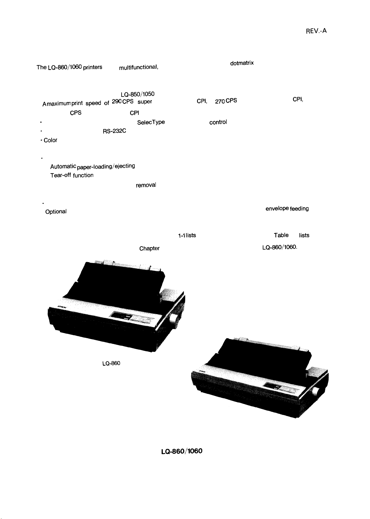
1.1 FEATURES
REV.-A
The
LQ-860/1080
features of the these printers
. Upward compatibility with the LQ-850/1050
. ~
maximum print
and of 90
o
Direct selection of font and pitch in
.
Both 8-bit parallel and
.
Color
printing capability
. Push and (optional) pull tractor feeding
.
Advanced paper handling:
AUtomatiC paper-loadin9/ejectin9
Tear-off
Printing of fanfold paper without
. Low-noise acoustics
.
Optional interface for the EPSON 8100 series
.
Optional
capability
Figure 1-1 shows exterior views of the printers,
the optional interface boards (refer to
printerS
speed of 290
CPS
in LQ mode at 12
funCtiOn
low-priced,
are
multifunction~ll,
are:
cps
in super
CPI
SelecT’YPe
RS-232C
single-bin and double-bin
serial interfaces
function
removal
Chapt[?r
24-pin printhead, impact
draft mode at
feature from the
of the cut sheet feeder (option)
Table
3 for more detailed information) for the LQ-8W106O.
10
CPI,
of
contrOl
cut sheet feeders which contains
1-1 lists
optional units available, and
dotmatrix
270 Cps
panel
printers. The main
in draft mode at 12
enveloPe feedin9
Table
CP1’
1-2
lists
LQ-860
Figure 1-1.
LQ-860/1060
1-1
LQ-106O
Exterior Views
Page 11
REV.-A
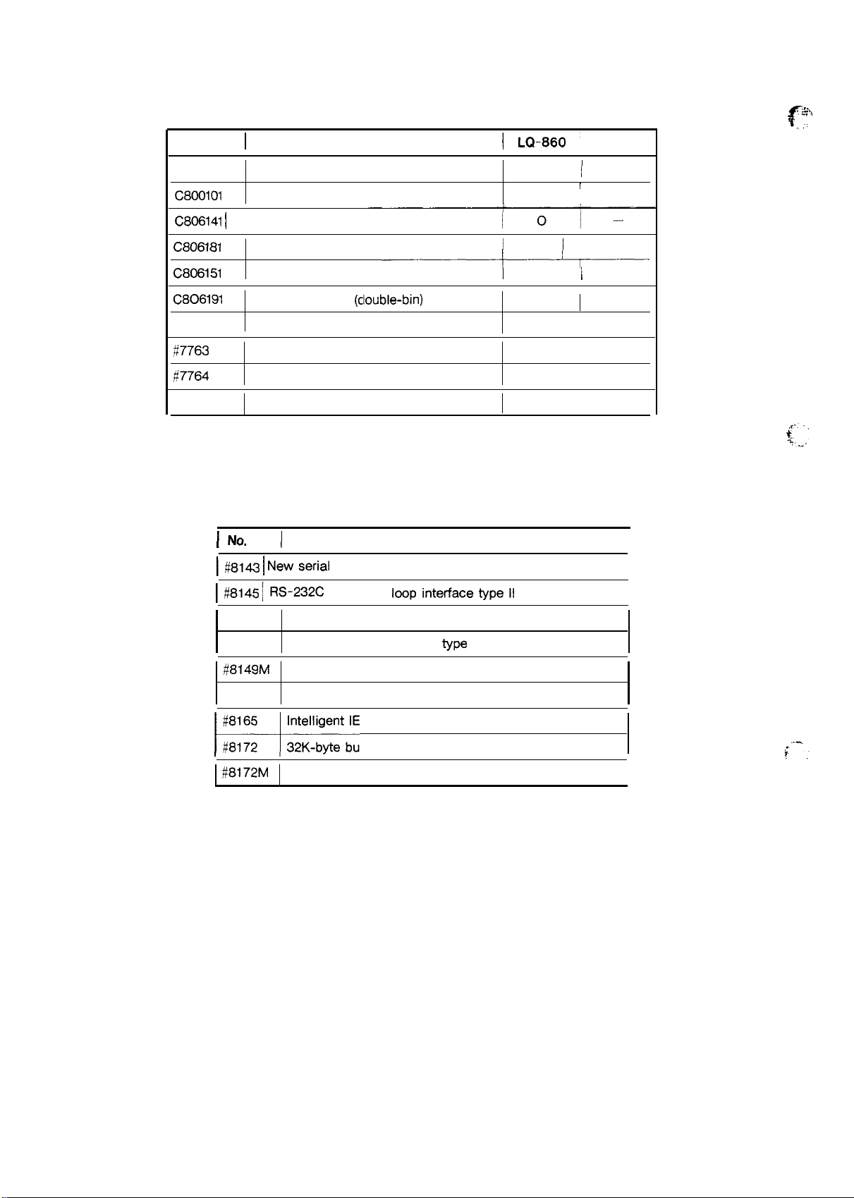
No.
C800071
C800101
I
Pull tractor unit
Pull tractor unit
Table 1-1. Optional Units
Name
I LQ-8601 LQ-106O
o
~
–
!
o
.+
.-. ,
r.
.,. .
C806141 I
C806181
C806151
C806191
#7762
87763
ff7764
#7407
Cut sheet feeder (single-bin)
Cut sheet feeder (single-bin)
Cut sheet feeder (double-bin)
Cut sheet feeder
Ribbon cartridge (black)
Ribbon cartridge (color)
Ribbon cartridge (film)
Multi font module
Table 1-2. Optional Interface Boards
I
No.
/
1#8143 I
1#8145
Newserial interface
IRS-232C current loopinterfacetypell
#8148
Intelligent serial interface
~
(clouble-bin)
Name
- ! 0
I
o
—
;
–
o
o
o
o
o
I
I
I
#8149
#8149M
#8161
l=-+---
#8172M
Intelligent serial interface
Intelligent serial interface type Ill
IEEE-488 interface
Intelligent IEEE-488 interface
32K-byte buffer parallel interface
128K-buffer parallel interface
type
II
I
1-2
Page 12
REV.-A
1.2 SPECIFICATIONS
This section describes the specifications for the printer without the Identity Module option.
Specifications not affected by firmware (hardware specifications) are the same whether or not the Identity
Module is installed.
1.2.1 Hardware Specifications
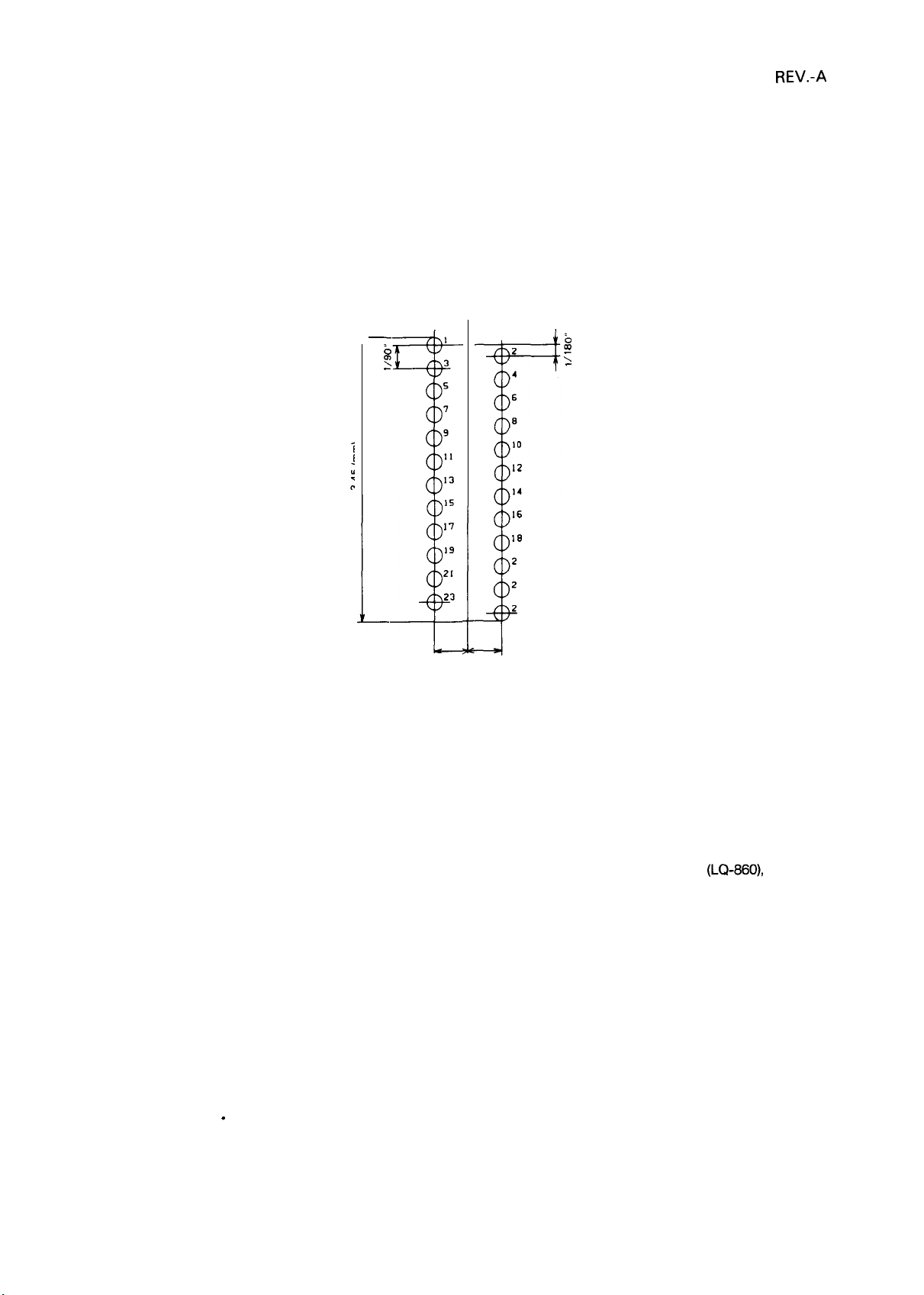
Printing Method
Pin Configuration
Serial, impact dot matrix
See Figure ‘I-2 (12x2 staggered, diameter: 0.2 mm).
—
0
y
-dz-
[~
Figure 1-2. Printhead Pin Configuration
I
3
15
r
17
19
21
23
[
“ 1/60”
‘ i/60’
o
m
T
4
6
8
10
12
14
16
18
20
22
24
Feeding Method
NOTES :
1. When using friction feed :
2. When using tractor feed:
Friction feed
Tractor feed (push: standard, pull : optional)
Adjust the paper release lever at rear position.
Use the paper tension unit.
Do not use continuous paper.
Do not use a single sheet paper shorter than 182 mm or longer than 257 mm
364 mm (LQ-106O).
Do not perform any reverse paper feed operations within the top 8.5 mm and bottom 22
mm area of the paper.
Do not perform reverse feed beyond than 1/6 “ after the paper end has been detected.
Do not use multi-part single sheet forms.
. Multiple copies for printing must be finished by pasting them together at the line or dots.
. Copy paper must be a carbonless multi-part paper.
a) When using push tractor feed:
. Adjust the paper release lever at center position.
“
Use the paper tension unit.
(LQ-860),
1-3
Page 13
REV.-A
“
Do not perform reverse feeding for more than 1/6 “.
“
Because accuracy of paper feed cannot be assured, do not perform reverse feeding
after the paper end has been detected.
b) When using pull tractor feed :
“
Adjust the paper release lever at front position.
“
Remove the paper tension unit and mount the pull tractor unit.
o
Use the paper path when a single sheet is inserted.
WV I
1~1 I
c) ‘A’’---
Adjust the paper release lever at front position.
Remove the paper tension unit and mount the pull tractor unit.
Do not loosen the paper between the platen and the pull sprocket.
Precisely the horizontal position of the pull sprocket and push tractor.
Do not perform reverse feeding for more than 1/6”.
Do not perform reverse feeding after the paper end has been detected.
U~ll Iy ~UW l-~Ull 11
“
“-’--
-’
‘-L
-’‘“ ‘---”-”
cX,LUl IGC7J
‘---A
.
“
Paper Loading Directions
Line Spacing
Line Feed Speed
Feeding Method
Friction without
Friction with
Tractor
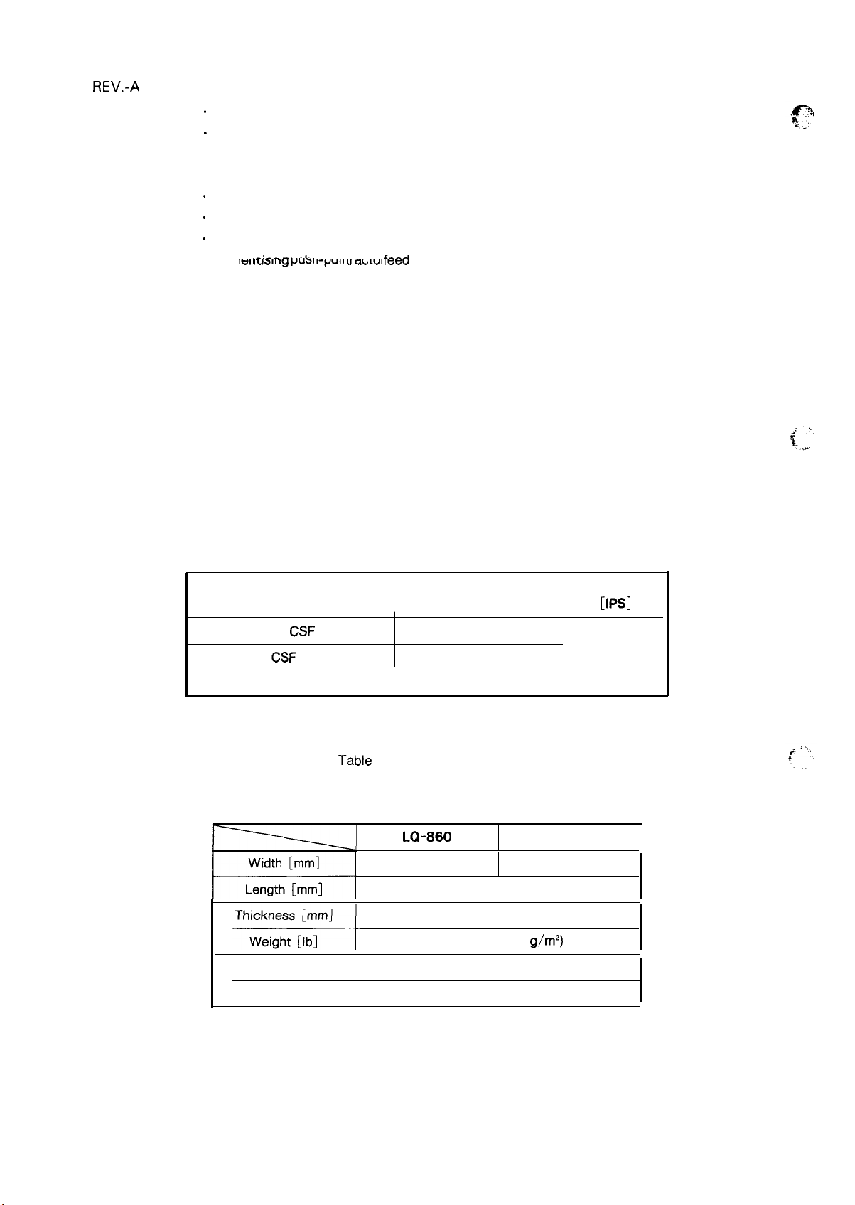
Paper specifications
Cut sheet paper
Inserted from the rear side
1/6” or programmable (min. 1/360”)
See Table 1-3.
Table 1-3. Line Feed Speeds
1 /6” line spacing
[ins/line]
CSF
CSF
I
Refer to
Table 1-4. Cut Sheet Paper Specified Conditions
Table
1-4.
LQ-860
182-257 (7.2 -10.1 “) 182-364 (7.2- 14.3”)
56.4
67.3
64.1
Continuous
I
I
LQ-106O
IIPS]
3.1
1
l--=%-l
*
Quality
Copies
182-364 (7.2-14.3”)
0.065-0.10 (0.0025-0.004”)
14-22 (52-82
Plain paper
Not available
1-4
9/m2)
Page 14
REV.-A
Continuous paper
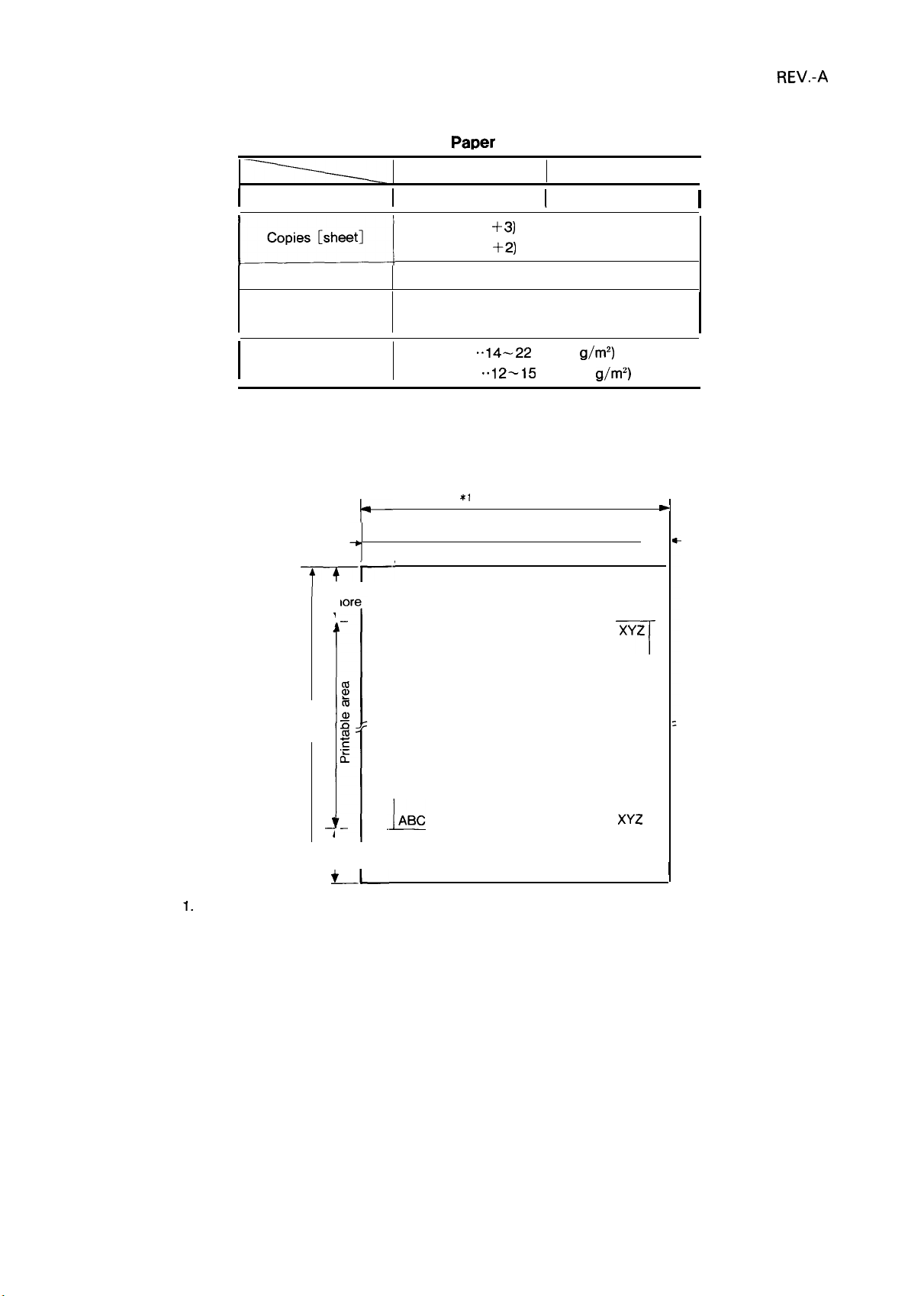
Printable Area
Cut sheet paper
Refer to Table 1-5.
Table 1-5. Continuous Paper Specified Conditions
I
Width [mm]
LQ-860
I
101-254 (4.0-10.0”) I 101-408 (4.0-16.0”)
4 (1 original
3 (1 original
+3)
+2)
1
at normal temperature
at all temperature range
H
Quality
Total Thickness
[mm]
Weight [lb]
See Figure 1-3.
i
--TY’
0.33”, 8.5 mm
I
or
I
I
—
I
t-
*3
i
0.085-0.32 (0.0025-0.01 2“)
1 sheet”
4 sheets” ””12-15 (40-58.2
7.2–10.1 *1 (14.4)”, 182–257 (364) mm
=
ABC
‘r
Plain paper
.”14-22
(52-82
Printable area
LQ-I 060
g/m2)
g/m2)
for each
XYZ
T
I
I
I
m
*3
—
NOTES :
7.2–14.3”,
182–364 mm
1
7
0.53”, 13.5 mm
or more
+L
1-
Values in the parentheses apply to the LQ-106O.
1.
2.
Printing is possible for approximately 42 mm after the bottom edge of a page has been
detected. Thus, the value 13,5 mm (lowest print position) is given for reference only. Paper
feed accuracy cannot be assured in the area approximately 22 mm (0.87”) from the bottom
edge of the page.
3.
0.12”, 3.0 mm or more when the 12”, 305 mm or less width paper is used. 0.58”, 15 mm or
more when the 13” width paper is used.
Figure 1-3. Cut Sheet Paper Printable Area
ABC
.J-
XYZ
-1
I
1-5
Page 15
REV.-A
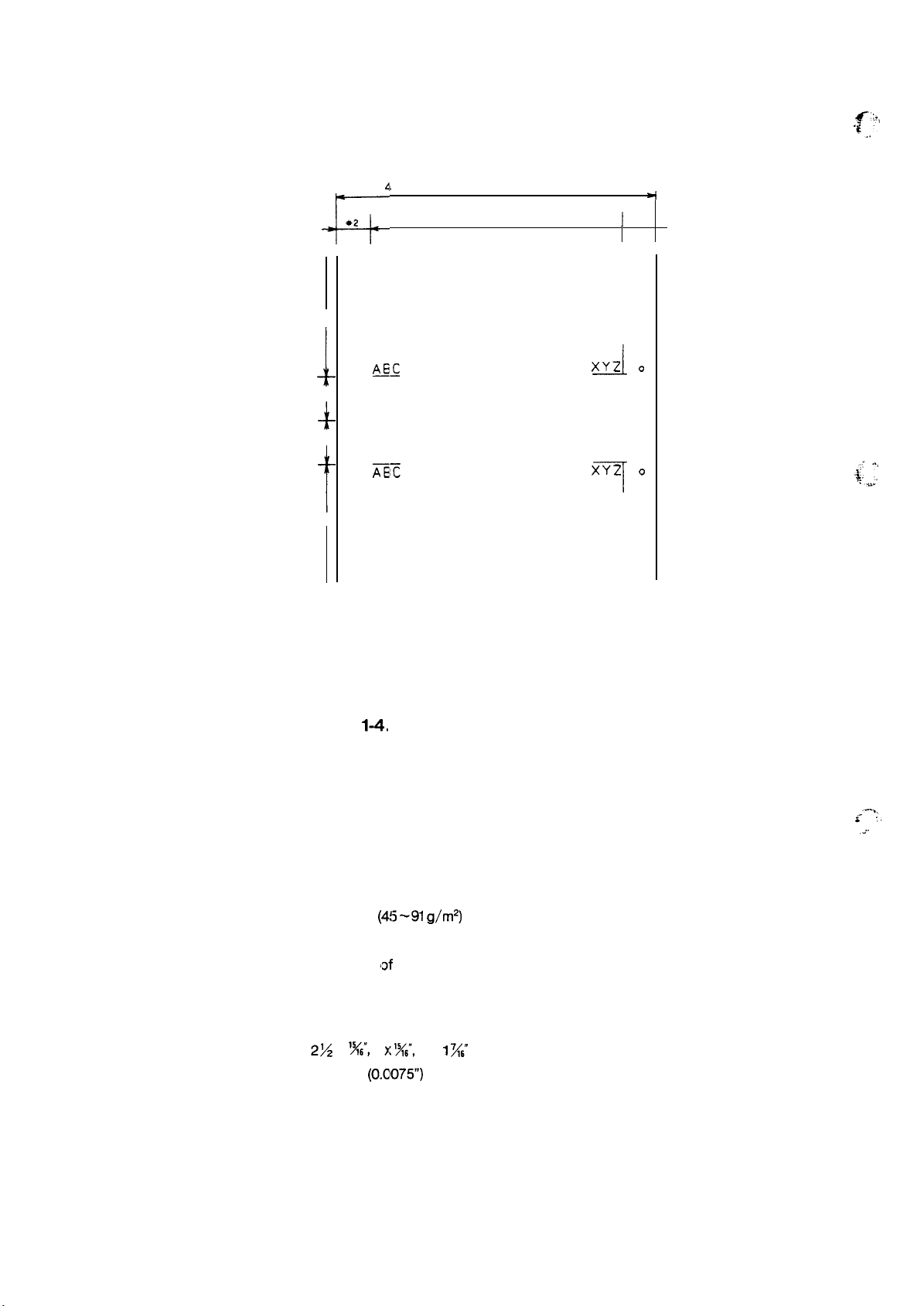
Fanfold (continuous) paper
0.35”, 9 mm
or more
0.35”, 9 mm
or more
See Figure 1-4.
*2
&
0
0
0
Printable
area
Printable
area
0
0
0
0
o
i
o
0
0
+
0
0
0
o
o
0
t
0
0
0
0
4!
- 10*1(1 6)”, 101
AE&
L
-------
AE~
T
0
- 254 (406)
Printable area
-----—.—-----------——
mm
XYZ
i
X’fz
I
0
T
4
*2
0
0
0
0
0
0
0
0
0
0
o
0
0
o
0
0
0
0
0
0
0
NOTES :
1. Values in the parentheses are apply to LQ-106O.
2. 0.47”, 12 mm or more when the 101 to 242 mm, 4 to 9.5” (101 to 378 mm, 4 to 14.9”) width
paper is used. 0.98”, 25 mm or more when the 254 mm, 10”, (381 to 406 mm, 15 to 16”) width
paper is used.
Figure
14.
Fanfold Paper Printable Area
Envelopes
Size
Quality
Thickness
NOTES :
Weight
NOTES :
Differences in thickness within printing area must be less than 0.25 mm (0.0098”).
1. Envelope printing is only available at normal temperature.
2. Keep the longer side
No. 6 (166 x 92 mm), No. 10 (240 x 104 mm)
Bond paper, xerographic copier paper, airmail paper
0.16-0.52 mm (0.0063-0.0197”)
12-24 lb (4!5-91
of
g/m2)
the envelope horizontally at setting.
3. Set the left of No. 6 envelope at the setting mark of the sheet guide.
Label
2% X
1%’s”,
4 x
%“,
4 X 1
Size
Thickness 0.19 mm
(0.C075”)
%“
max.
NOTES: Thickness excluding the base paper must be less than or equal to 0.12 mm (0.0075”).
.-..
f ;,
,-,,
1-6
Page 16
REV.-A
NOTES :
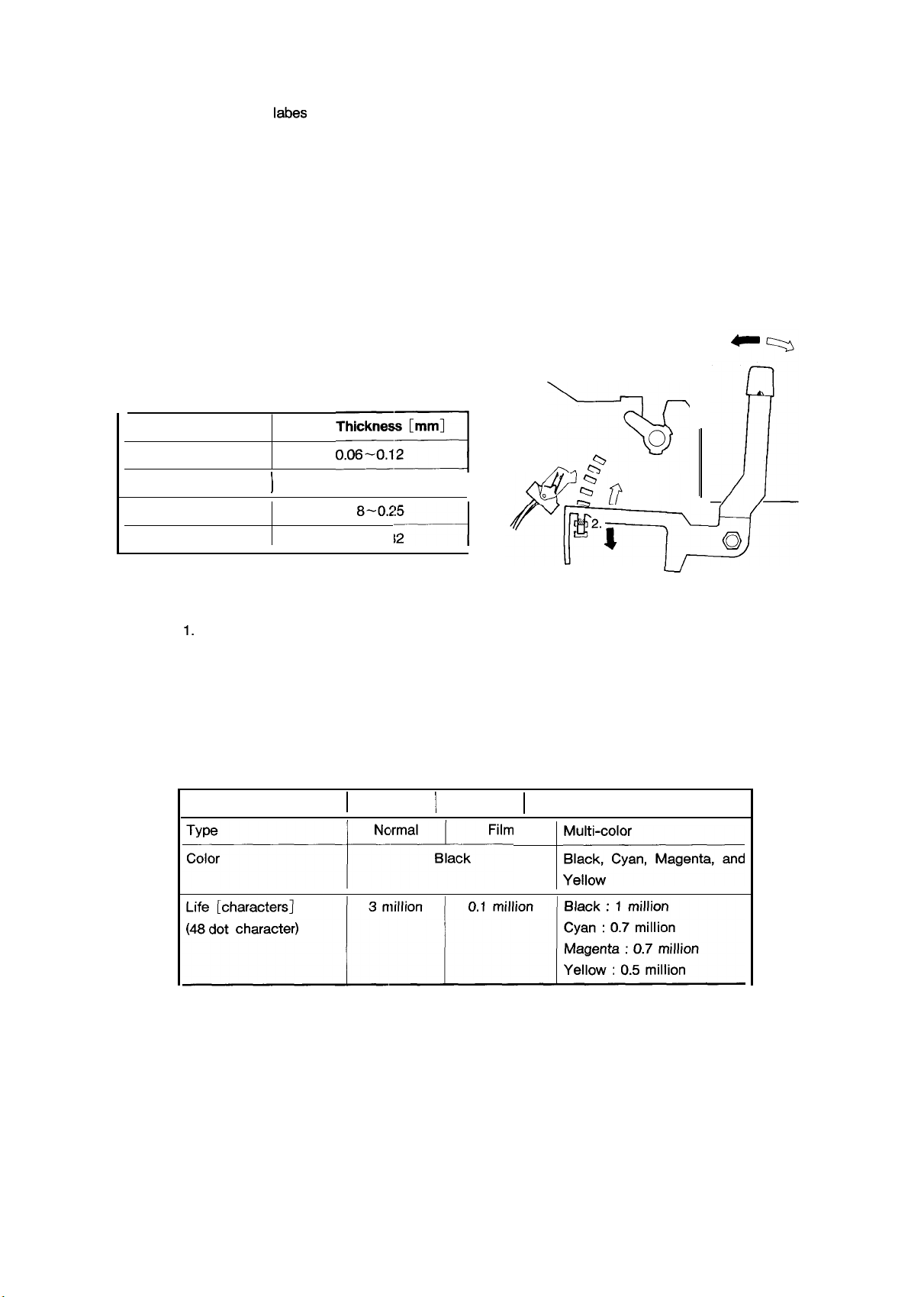
Lever Adjustment
1. Printing of
2. Labels must be fanfold.
3. Labels with pressure-sensitive paper must be jointed by pasting along the dots or lines, and
the total thickness must be less than or equal to 0.3 mm (0.0118”) to be printed out under
conditions that must be between 5 to 35-C and 10 to 80°/0 RH.
4. Examples of Iavels: AVERY CONTINUOUS FORM LABELS
Table 1-6. Lever Adjustment
Lever Position
2nd
3nd
4th
5th
Iabes
is only available at normal temperature.
AVERY MINI-LINE LABELS
See Figure 1-5 and l-able 1-6.
Paper Thickness
0.06-0.1:1
I
0.13-0.17
0.1
8-0.:!5
0.26-0.32
[mm]
I
+
~
NOTES :
Ribbon Cartridge
1.
2.
Ribbon Model No.
w%k’i’m
u
Figure 1-5. Head Adjustment Lever Positioning
When printing density becomes lighter, set the head adjustment lever one position lower.
When using thicker paper than shown in the above table, set the head adjustment lever to
the 6th or higher appropriate position by performing the self-test operation.
See Table 1-7.
Table 1-7. Ribbon Cartridge Specification
I
#7762 I #7764 I #7763
:ii:;:nMagenta7and
1-7
Page 17
REV.-A
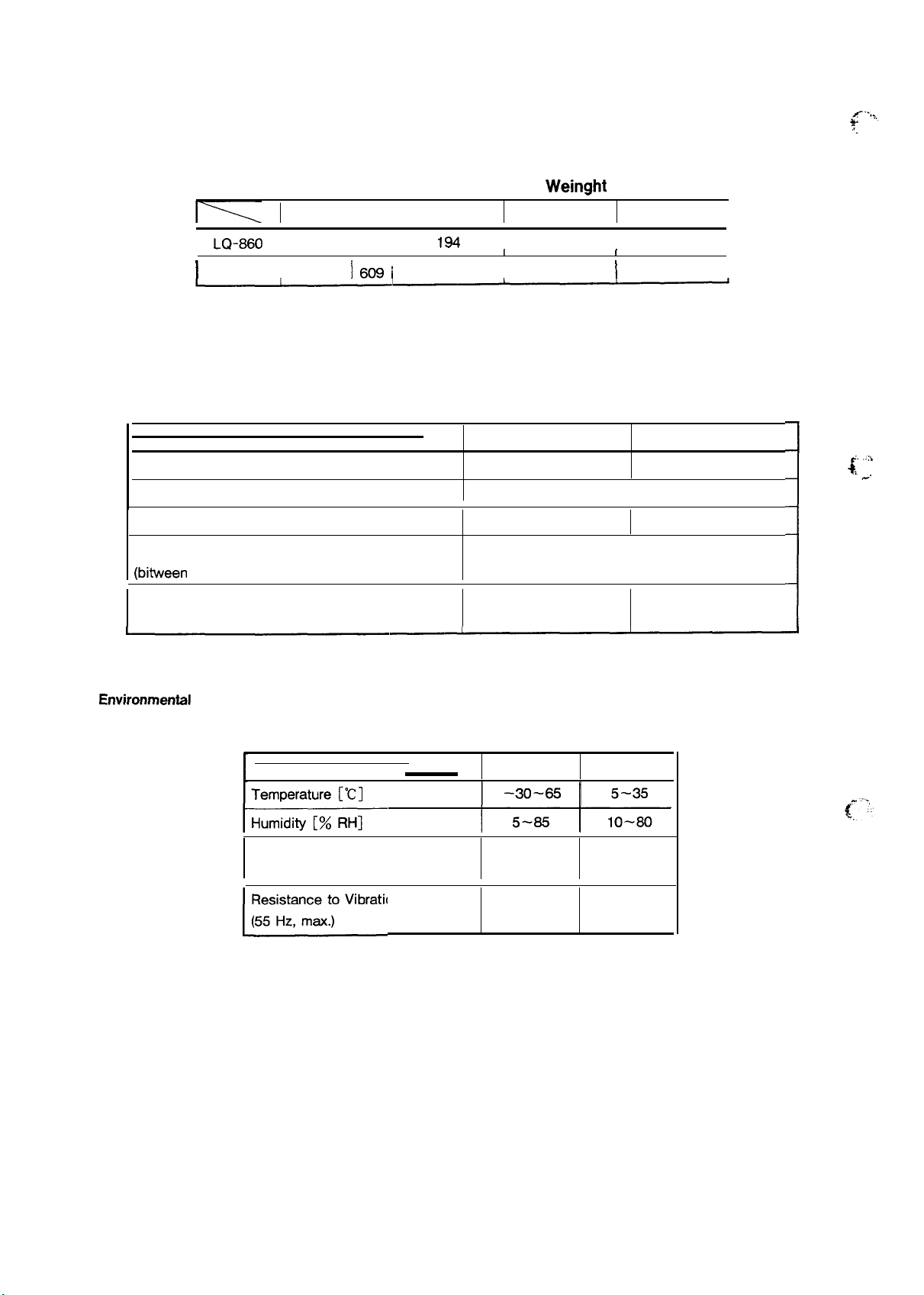
Dimensions
Weight
I LQ-860 I
I
I
LQ-106O
See Table 1-8 (Details are shown in Figures A-36 and A-39.)
See Table 1-8.
I
NOTE : Excluding paper feed knob and sheet guide.
Electrical Specifications
Voltage [V AC]
Frequency Range [Hz]
Rating Current [A]
Insulation Resistance [M ohm] min.
Oitween
AC line and chassis)
See Table 1-9.
Table 1-8. Dimensions and Weinght
Width [mm]
469
I 609 i
Height [mm]
194
194
Depth [mm]
399
I
I
399
I
Table 1-9. Electrical Specifications
100-120 V Version
108-132
2
Weight [Kg]
I
1
I
220-240 V Version
49.5 -60.5
10
10
13
198-264
I
I
I
I
~. .:,,
“
-,
1
Dielectric Strength [V AC, rms]
(1 minute, between AC line and chassis)
Conditions Refer to Table 1-10.
Table 1-10. Environmental Conditions
I
Resistance
(within 1 ms)
Resistance to Vibration [G]
to shock [G]
L@_
1250
Storage
2
0.50
3750
Operating
(“;,
1
0.25
1-8
Page 18
Reliability
. . . . .
REV.-A
MCBF
MTBF
LQ-860 :
LQ-106O :
Printhead
Safety
life
Approvals
Safety standards
Radio Frequency
(RFI)
Interference
1.2.2 Firmware Specifications
Control Code
Printing Direction
Input Data Buffer
Character Code
Character Set
Family
Font
Printing Mode
NOTES :
A condensed mode for 15
0
/0)
0
/0)
printhead)
5 million lines (excluding
(MCBF . . .
4000
6000
(POH . . . .
200
UL478
Mean Cycles Between Failure)
POFI
(duty 25
POI-I
(duty 25
F)ower
On Hours)
milion
strokes/wire
(U.S.A. version)
CSA22.2#f54
VDE0806 (TUV)
FCC
class
(European version)
B (U.S.A. version)
VDE0871 (self-certification)
(Europe version)
ESC/P-84C
Bidirectional with logic seeking
6 K-byte or none ( DIP SW 1-8 selectable)
8 bits
96 ASCII, 14 international, and 1 Legal charactersets
Roman:
Sansserif:
Roman:
Sansserif:
Draft:
Printing quality
Character pitch (10, 12, 15
No. O
No. 1
10, 12, 15, Proportional
10, 12, 15, Proportional
10, 12, 15
(Draft/LQ)
CPI
or Proportional)
Condensed
Double-width
Double-height
Emphasized
Double-strike
It:alic
Lhderlined
Double-underlined
C)verscore
Strike-through
Shadow/Outline
CPI
characters is not available.
Print Speed
Print Columns
Refer to l-able 1-11.
Refer to l-able 1-11.
1-9
Page 19
REV.-A
Table 1-11. Printing Mode
10
12
15
Print
Pitch
Conden- Emphas- Double
sed
0 0
ized
Width
0
1
1
0
1
1
x
o
1
0
0 0
1
1
0
1
1
x
o
1
0 0 0
1
Character
Pitch
[cPI]
10
5
10
5
17.1
8.5
12
6
12
6 68
20 225
10 113
15
15
Printing Speed
Printable Columns
[CPS]
Draft
225”’
113
113
56
193
LQ
LQ-860 LQ-1060
75
38
75
38
129
96 64
270 90 96
135
135
45
90
45
150
75
338
169
113 120
56
80
40
80
40
137
69
48
96
48
160
80
60
136
68
136
68
233
117
164
82
164
82
272
136
204
102
%oporticmal
‘proportional
Super/
subscript
1
0
1
1
o
x
x
x
o
7,5
7.5
8.6 64
20
1
4.3
10
1
x
o
17.1
40
1
8.6
20
o
x
o
12.8
30
1
6.4
15
1
x o
25.7
60
1
12.8
30
169 113
84
56
Ignored
—
150
32
—
—
—
—
75
129 Max. 137
300
64
150
—
96 Max. 103
225
—
—
–
—
—
—
48 Max. 51
113
193
450
96
225
120
60
204
102
Max. 69 Max. 117
Min. 160
Min. 272
Max. 34 Max. 59
Min. 80
Min. 136
Max. 233
Min. 320
Max. 69
Min. 160
Min. 544
Max. 117
Min. 272
Max. 175
Min. 240
Min. 408
Max. 87
Min. 120 Min. 204
Max. 206
Max. 349
Min. 480 Min. 816
Max. 103
Min. 240
Max. 175
Min. 408
—
.
.
r’
,
1-10
Page 20
*
1 :
290
CPS
NOTES : 1.
at super draft printing (DIP SVV
Max. means the value when
Min. means the value when
2.
“
—“ means that LQ character set is automatically selected when proportional pitch is
3.
1-6
is off).
t:he
maximum width characters are printed.
the
minimum width characters are printed.
specified.
REV.-A
Character Matrix
(Normal Character)
1
2
3
4
5
6
7
r
Ascender Area
8
9
;
>
10
II
i
.
12
,
13
14
10.
15
16
/7
18
19
20
21
22
23
24
Descender Area
Character Width
Ascender Area
(15pitch )
Face
Width (al
See Figure 1-6 and Table 1-12.
R
I
G
H
T
s
P
A
c
E
(a
2
)
(CW)
J
(Superscript Character)
Pin Nos. 17 to 24 are not used when superscript
printing.
—
2L
3E
4F
5T
6
7s
Eip
9A
10
c
II E
12
13
14
15
16
[
(Subscript Character)
Pin Nos. 1 to 8 are not used when subscript printing
9
10
L
II
E
12
F
13
T
14
15 s
16
p
17
A
18 c
19
E
20
21
22
23
24
[
R
A
H
T
s
P
A
c
E
—
—
R
;
H
T
s
P
A
c
E
—
Figure 1-6. Character
1-11
Matrix
Page 21
REV.-A
Character Size See Table I-12.
Table 1-12. Character Matrix and Character Size
Printing Mode
DRAFT, 10 pitch
DRAFT, 12 pitch
DRAFT, 15 pitch
DRAFT, 10 pitch, condensed
DRAFT, 12 pitch, condensed
LQ,
10 pitch
LQ.
12 pitch
LQ,
15 pitch
LQ,
10 pitch, condensed
LQ, 12
pitch, condensed
-Q, proportional
.Q, proportional, condensed
Face Matrix
9 X 23
9 X 23
9
X 16
. . .
. . .
29X 23
29X 23
15X 16
. . .
. . .
max. 37X 23
min. 18X 23
. . .
. . .
HDD
120
120
120 1.0 X 2.3 120
240
240
360 2.0x 3.2
360
360
360
360
360 2.6X 3.2
360
360
360
Character Size
H. XV. (mm)
1.9x 3.2
1.9x 3.2
. . .
. . .
2.0 x3.2
1.0X 2.3
. . .
. . .
1.0x 3.2
. . .
. . .
Unit
ESC
120
120
120
120
180
180
180
180
180
180
180
Sp
: .:.,
P
.
.-,:. . .. .
.
*
“=-.
+
.Q, proportional,
-Q,
proportional, super/subscript, condensed
NOTES : 1.
2.
3.
4.
super/subscropt
“HDD”
means the
“Face matrix” and “character size” indicate the size of maximum characters and this value
will be changed condition of paper, ribbon, and etc.
“Unit
ESC SP”
can be specified with
“.. .“ indicated that the character matrix is reformed by firmware. Character width becomes
haJf
of a non-condensed character.
Horizontid
indicates the minimum length which is added to the right of the character that
max. 28X 16
min. 12x 16
. . .
. . .
360
360 0.7X 2.3
360
360
1.8x 2.3
. . .
. . .
dot density, and the “Unit” shows the number
ESC)
sp control code.
160
180
of dots per inch.
... %
.,.
f ‘“’
.“”
1-12
Page 22
1.3 INTERFACE OVERVIEW
The LQ-860/1060 has both 8-bit parallel interface and RS-232C serial interface as standard. They can be
selected by DIP switches 2-3 and
2-4 respectively. (This detail of DIP switch settings, refer to Table 1-20.)
REV.-A
1.3.1 8-bit Parallel
Data Transmission
Interface
Mode
Synchronization
Hand Shaking
Logic Level
Data Transmission Timing
Adaptable Connector
Connector Pin Assignment
Select/Deselect
(DC1/DC3)
Control
BUSY
ACKNLG
DATA
STROBE
Specifications
8-bit
pallarel
By
STROB=
By BUSY and
pulse
ACKNLG
(either or both)
TTL compatible
See
Figure
1-7.
57-30360 (AMPHENOL) or equivalent
(See Figure 1-8.)
Refer to Table 1-13.
Refer to Table 1-14.
~**,~
w
NOTES :
Transmission time (rising and falling time) of evev
input signal must be less than 0.2
Figure 1-7. 8-bit Parallel Interface Data Transmission Timing
1.
2.
3.
4.
5.
6.
7.
8.
9.
10.
I 1.
12.
13.
I 4.
15.
16.
17.
18.
19.
GNO (
Pair
GNO (
20.
21.
GND
( Pair
G?4D [ Pair
22.
GND (
23.
24.
GND
( Pair w;th6.)
25.
GND
( Pair w;th7.)
26.
GNO
(
GNO
( Pair w,th9.)
27.
28. GNO
(
29.
GNO
(
30.
GNO
(
31.
~T
32. ERROR
33.
GNO
34. NC
35.
+5V
36.
5LCTIN
witn 1.)
Pair
w;th2.)
with
3.)
w;ti14.)
Pair
w;tn5. )
Pair “:t~s.)
Pair with
10. )
Pair w;th
I 1.)
Pair w;tn
12. )
IAS.
Figure 1-8. 36-Pin Printer Side Connector
1-13
Page 23
Table 1-13. 8-bit Parallel l/F Connector Pin Assignments
f’;’.
Pin No.
1
2
3
4
5
Signal
STROBE
DATA1
DATA2
DATA3
DATA4 23
6 DATA5
7
8
DATA6
DATA?
9 DATA8
10 ACKNLG
11
BUSY
12
13
SLCT
PE
Return
19
20
21
22
24
25
26
27
28
29
30
—
1/0
I
Strobe pulse to read the input data. Pulse width must
be more than 0.5
Description
,US.
input data is latched after
falling edge of this signal.
Parallel input data to the printer.
I
“HIGH” level means data “1”.
I
“LOW” level means data “O”.
I
I
I
I
I
I
This pulse indicates data are received and the
0
printer is ready to accept next data. Pulse width is
approx. 11
“HIGH” indicates printer can not accept data.
0
“HIGH’ ’indicates paper-out.
0
/s.
This signal is effective only when ERROR signal is
“LOW”.
+5V
Always “HIGH”. (Pulled up to
o
through 3.3 K
ohms resistor.)
14
15
16
17
18
19 to 30
31
32
33
34
35
36
AUTOFEED-XT –
NC
GND
Chassis
GND
NC
GND
INIT
ERROR
GND
NC
+5V
SLECT-IN
—
—
—
16
.
—
—
—
—
—
—
If this signal is “LOW” when the printer is initialized,
I
a line feed is automatically performed by input of
“CR” code (Auto
—
Not
USed.
—
Ground for twisted-pair.
—
Printer chassis ground.
—
Not used.
—
Ground for twisted-pair.
Pulse (width : 50
i
LF).
,US
min., active “LOW”) input for
printer initialization.
0
“LOW indicates that some error has occurred in the
printer.
.
Ground for twisted-pair.
—
Not
USed.
+5V
Always “HIGH”. (Pulled up to
o
through 3.3 K
ohms resistor.)
If the signal is “LOW” when printer is initialized, the
I
DC1/DC3
control is disabled.
NOTES :
“Direction” of signal flow is as viewed from the printer.
1.
2.
“Return” denotes “TWISTED PAIR RETURN” and is to be connected at signal ground level.
1-14
Page 24
REV.-A
As to the wiring for the interface, be sure to use a twisted-pair cable for each signal and
never fail to connect the return side. To prevent noise, cables should be shielded and
connected to the chassis of the host computer and the printer.
Table 1-14. Select/Deaelect Control
ON-LINE
Sw
OFF-LINE
ON-LINE
SLCT-IN
HIGH/LOW
HIGH
LOW
DCI /DC3
DCI
/DC3
DC1
DC3
DC1
DC3
ERROR
LOW
HIGH
HIGH
HIGH
HIGH
HIGH
LOW/HIGH (During
data entry)
LOW/HIGH (During
data entry)
LOW/HIGH (During
data entry)
LOW/HIGH (During
data entry)
-
BUSY
NOTES : 1. In Table 1-14, it is assumed that no ERROR status exists other than
OFF-LINE mode.
2. Once the printer is deselected by the
state until the
is received.)
3. The
DC1
and
No. 36 when the parallel interface unit is used) is HIGH and the printer is initialized.
4. The
SLCT-IN signal is “LOW” when the printer is initialized. At this time the DC1/DC3
printer select/deselect control is invalidated, and these control codes are ignored.
DC1
code is input. (In the deselected state, input data is ignored until
DC3
codes are enabled only when the SLCT-IN signal (Input Connecter Pin
DC3
code, the printer will not revert to the selected
ACKNLG DATA
No pulse
Pulse output after
entry
Pulse output after
entry
Pulse output after
entry
Pulse output after
entry
that attributable to the
ENTRY
Disable
Enable
(Normal
Process)
Enable
(Waits
DC1
. See
NOTE 2)
Enable
(Normal
Process)
DC1
1-15
Page 25
REV.-A
1.3.2 RS-232C Serial Interface Specifications
Data Transmission Mode RS-232C serial
Synchronization
Handshaking
Asynchronous
(By
DTR (FIEV)
(Refer to Table 1-15 and Figure 1-9.)
Table 1-15. Serial Interface Handshaking
signal or X-ON/OFF Protocol
DTR
Signal
MARK
SPACE
DTR
(REV) Signal
MARK
SPASE (
+12V)
X-ON/OFF protocol
X-OFF (DC3/13H)
X-ON (DC1/11 H)
I
(–12V)
-----------
~,
~
6Kbyte
~
When the number of bytes remaining in the input buffer
reaches 256 or less, the signal level goes to MARK, or
and X-OFF code is sent to the host computer. This
indicates that the printer is not ready to receive data.
When the number of bytes remaining in the input buffer
reaches 528 or more, the signal level goes to SPACE, or
an X-ON code is sent to the host computer. This indicates that the priter is ready to receive data.
Eq
:
,
1
!j28byte 256byte
1
[
X-ON X-OFF
:
1
1
1
[
:
Obyte
Description
Input Buffer Vacant Area
X-ON/X-OFF Protocol
Word Length
Start bit:
Data bits:
Parity:
Stop bits:
Bit Rate
Logic Level
Figure 1-9. RS-232C Interface Handshaking
1
8
Odd, Even, or none
1 bit or more
300, 1200, 9600, or 19200 BPS
EIA level, IMARK: logical 1 (–3- –27 V)
!SPACE
: logical O
1-16
(+3-
+27 V)
>,. ,-,
Page 26
REV.-A
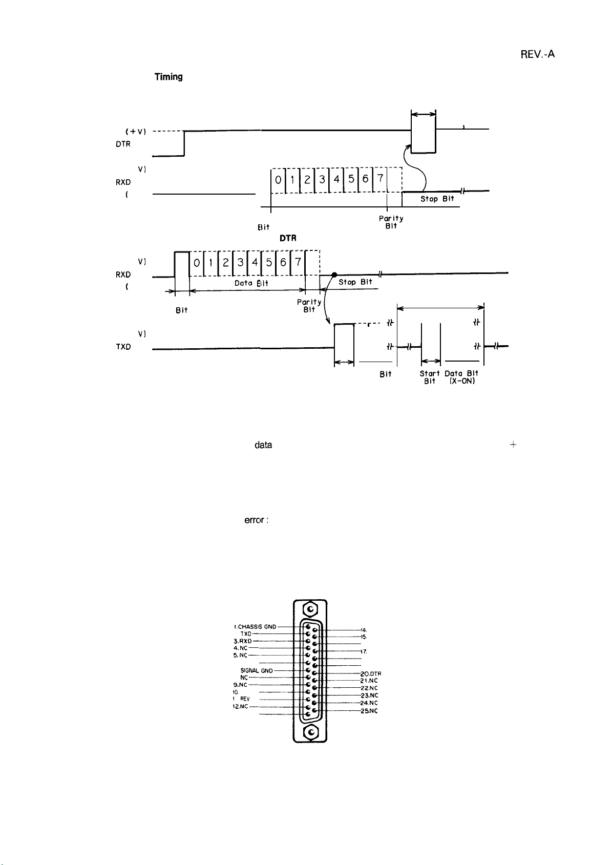
Data Transmission
[
+V)
DTR
r
( – VI
( +
v]
RXD
--------------------y
(
-v)
( +
v]
[
-v)
( +
v)
g:F[<[[[iFEE3
RXD
TXD
( -v]
Timing
Start
Blt
See Figure 1-10.
:!S!12131:15-FF
Start
Elit
Elit
Data
+
x-ON/X-OFF
DTR
Handshake
P\ri~y
Data Bit
,+apB,+/—
--- --
Start Data
Bit (X-OFF)
Protocol
-- --
[[
::;
P~rlty
4
i~
if
4+
Bit
‘T”
~
s
‘T “
-- --
–
-- --
.[[’
S;;;t D~t:OB;t
ik
IF
*
4+
NOTES :
1. The value of “T” varies according to the input data.
2. The word structure of serial
1 or more stop bits.
Error Detection
Connector
Connector Pin Assignments
clata
is 1 start bit + 8 data bits+ parity (Odd, Even, or none)
Figure 1-10. Serial Data Transmission Timing
errcr:
Parity
Overrun error:
Framing error: Ignored
D-SUB 25-pin connector (See Figure 1-11.)
Refer to Table 1-16.
LCHASSI
2.
TxD-—
3.RXD—
4,NC—
5.NC—
6.Nc-—-
7.
SGNAL
8. Nc—-
9.NC—
tO.
NC —
I
l,
REv
—
f2.NC—
13. NC —-
“x” is printed.
Ignored
t4.
NC
i5.
NC
16. NC
17,
NC
16 NC
19. NC
20.QTR
21.NC
22.NC
23.NC
24.NC
25NC
+
Figure 1-11. Serial Interface Connector
1-17
Page 27

REV.-A
Table 1-16. RS-232C Serial l/F Connector Pin Assignments
Pin No.
2
20
11
3
7
1
Signal
TXD
DTR
REV (=2nd RTS) o Same as
RXD
SIGNAL
CHASSIS
GND
GND
Dir.
o
o
I
–
–
Transmit data.
Indicates when printer is ready to receive data. “MARK”
level
indictes
Receive data.
Signal (Logic) ground level.
Printer chassis ground.
printer is not ready to receive data.
DTR.
NOTE : “Direction” of signal flow is as viewed from the printer.
Description
1-18
f ‘:,
.,
Page 28
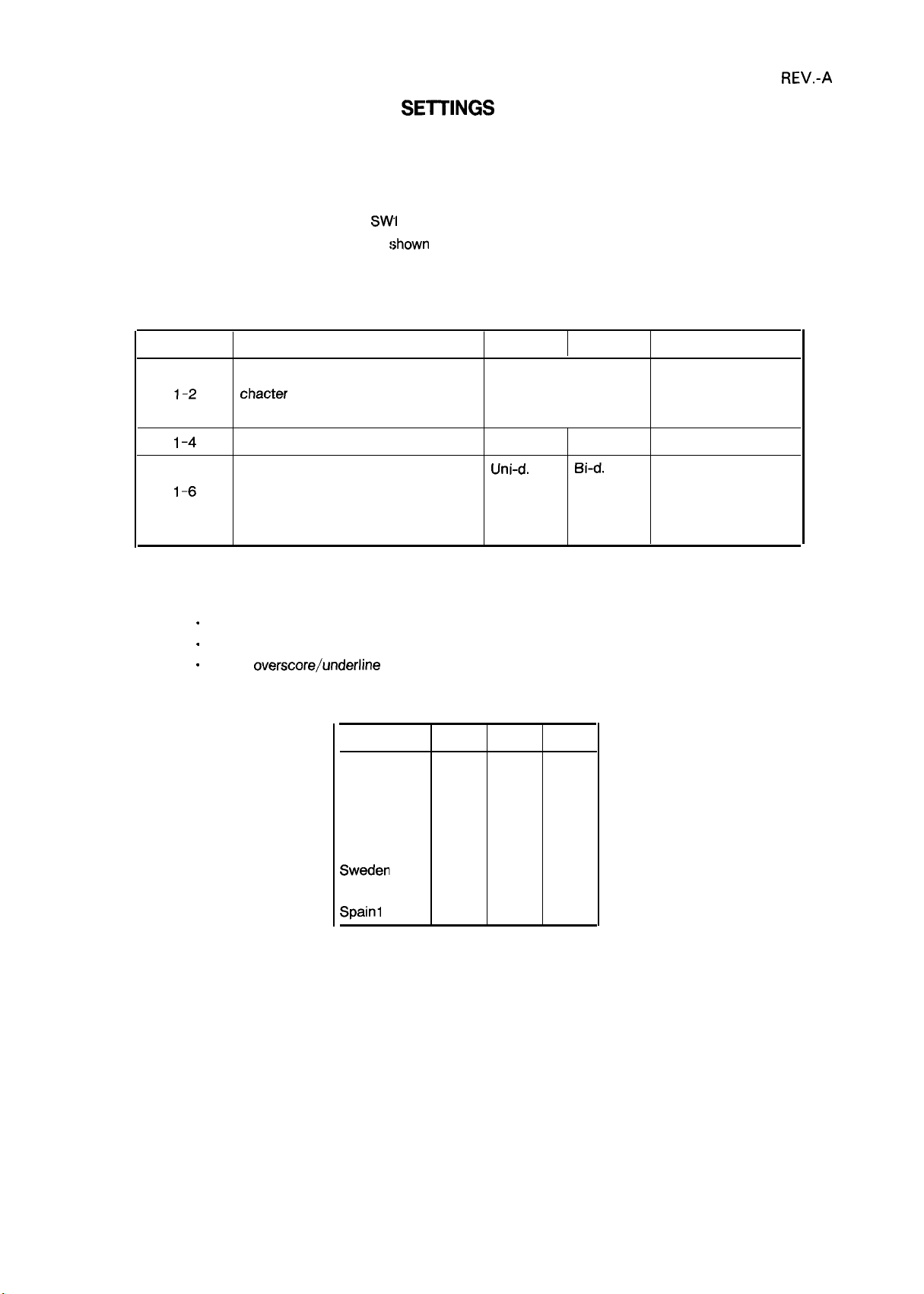
1.4 DIP SWITCH AND JUMPER SEITINGS
This section describes DIP switch settings and jumper settings on the JUNMM board.
1.4.1 DIP Switch Settings
REV.-A
The DIP switches that users can set are
the control panel, and have the functions as
DIP switches are read only when the printer power on or an INIT signal is input.)
SW”I
and SW2. These switches are positioned at the left side of
:>hown
in Tables 1-17 through 1-21, (note that the status of the
Table “I-17. DIP Switch 1 Settings
DIP SW.
1-1
1-2
International
chacter
set
Function
ON
See Table 1-18.
OFF
1-3
1-4
1-5
1-6
1-7
1-8
* 1 : “
Graphic print” means follows
a) Bit image printing
b) Multi pass printing
Code table select
Graphic print direction”’
Super draft
CSF mode
Input buffer
“
30 dots graphics
“
Double height character
o
Double
overscore/underline
Graphic
Uni-d.
off
Valid
None
. Orator/Orator-S font
. Double-strike
. Violet, Orange, Green color printing
Italic
Bi-d. OFF
On
Invalid
6K-byte
Factory Setting
ON
ON
ON
OFF
OFF
OFF
OFF
Table 1-18. International Character Set Designation
Country
U. S. A.
France ON ON OFF
Germany ON
U. K.
Demarkl
Sweden
Italy OFF OFF
Spainl
1-1
ON ON
ON OFF OFF
OFF ON
OFF ON OFF
OFF
1-2 1-3
ON
OFF
OFF OFF
ON
ON
ON
NOTE : The above settings can be changed to any country’s characters set by inputting ESC R control
codes.
1-19
Page 29
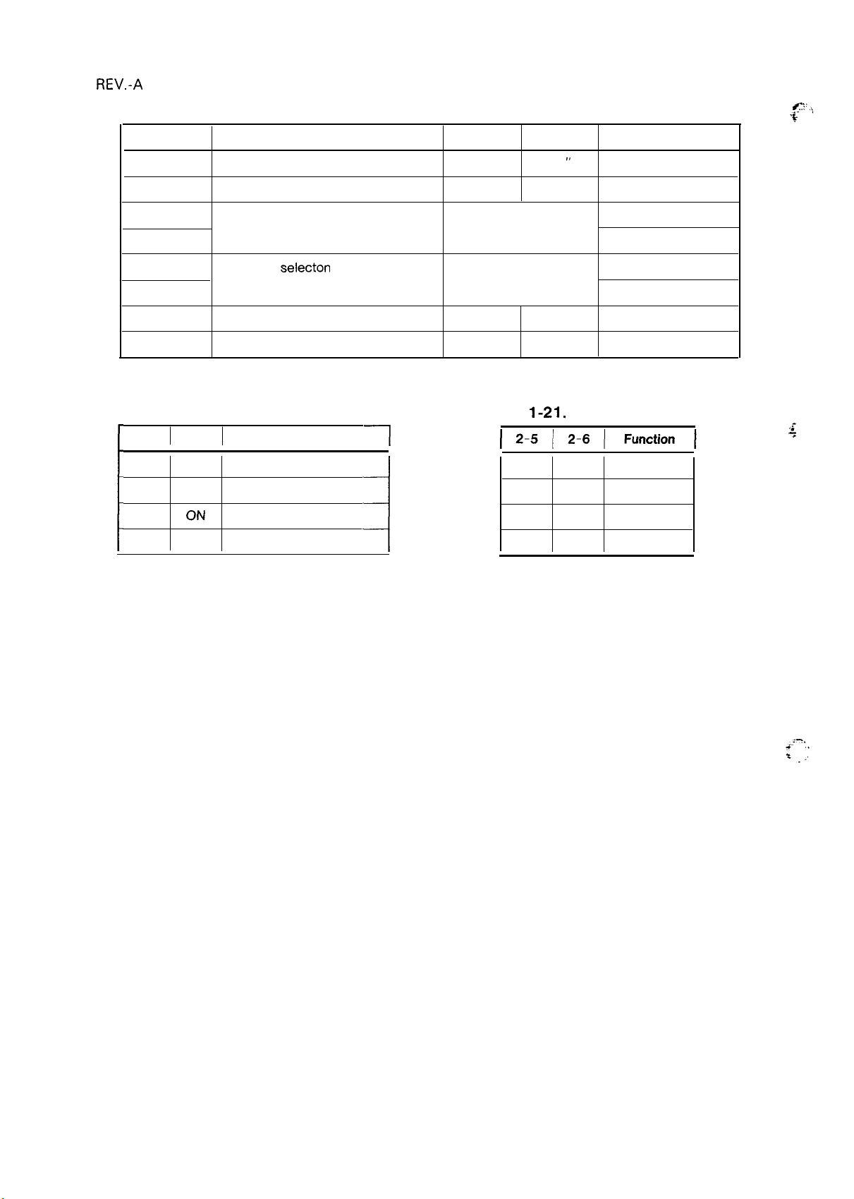
REV.-A
DIP SW.
Function
Table 1-19. DIP Switch 2 Settings
ON OFF
Factory Setting
q
‘g
2-1
2-2
2-3
2-4
2-5
2-6
2-7
2-8
Page length
1“ skip-over perforation
Interface selection
Baud rate
Auto fear-off mode
Auto LF
selecton
Table 1-20. Interface Selection
2-3
OFF
ON
OFF
ON
2-4
OFF
OFF
ON
Function
8-bit Parallel
Serial, Even parity
ON
Serial, Odd parity
Serial, None parity
19,200
9,600
1,200
300
OFF
OFF
OFF
OFF
OFF
OFF
OFF
OFF
.*-
-%
12”
Valid Invalid
See Table 1-20.
See Table 1-21.
Valid Invalid
Valid
Table
11
“
Invalid
1-21.
Baud Rate Selection
1
OFF
ON
OFF
1
ON ON
OFF
OFF
ON
1-20
Page 30
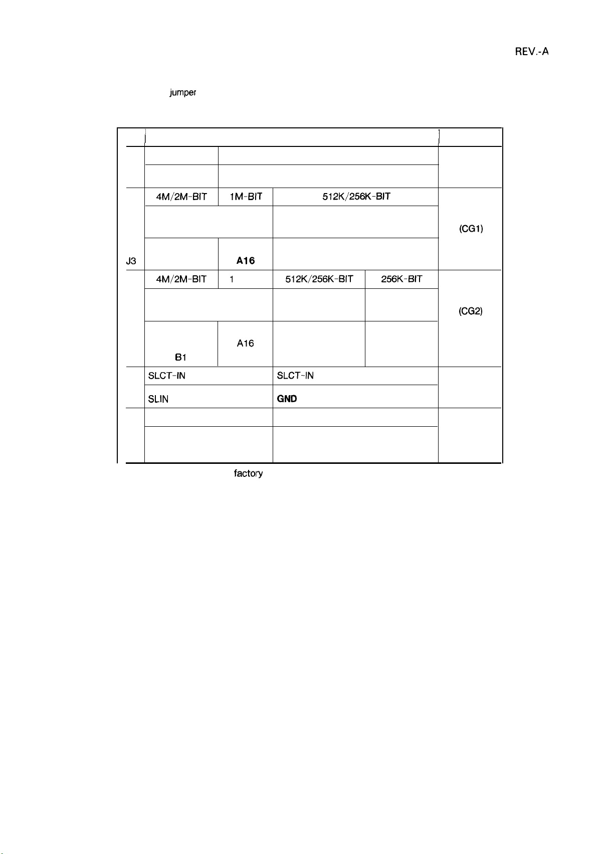
1.4.2 Jumper Settings
REV.-A
Table 1-22 shows the
No.
/
JI
4M/2M-BIT IM-BIT
J2
J3
4M/2M-BIT
J4
J5
J6
SLCT-IN inable
jumper
settings.
Table 1-22. Jumper Settings
Type
27256 27512
256
MASK-ROM
B4
RD
MASK-ROM
B4
RD
B1 B1
A16
1
M-BIT’
A16
+5 +5
+5 +5 +5
SLCT-IN disable
512
512K/256K-BIT
512K/256K-BIT
ROM
RD RD
B2
ROM
RD
256K-BIT
RAM
WR
)
Location
6A
3A
(CG1)
4A
(CG2)
J7
SLIN
LQ-860
J8
Close
J9
Open
NOTE : Bold indicates the
factotw
GND
LQ-106O
Open
Open
settings.
1-21
Page 31

REV.-A
1.5 SELF-TEST OPERATION
The LQ-860/1060 printer has the following self-test operation. The control ROM version No. and the DIP
switch settings also printout when the self-test is performed.
Table 1-23 lists the self-test operating instructions and Figure 1-12 shows the self-test printing.
Table 1-23. Self-Test Operation
Type-face
Draft
,-
Lu
Start
Turn the power ON while
pressing the LINE FEED switch.
Turn the power ON While
pressing the FORM FEED switch.
Push the ON LINE switch, and turn the
power OFF.
Draft mode
!
“
#$%&
f
“
#$%&
‘ ( )*+ , -
“ #$%&‘ ( )*+, -. /C)12345676g : ; ~ =
‘ ( )*+ , –
#$%&
‘ (
$%&
=
& “ ( )*+, -- /0123456789: ;
‘
( )*+, -. /0123456789: ;
()*+,
)*+,
)x+,
‘ ( )*+, -
‘ (
)%+
,-.
/0123; 456789 --
-./,oI234567B9,
-./olz3456789:;
*+,-./ol234567~9:
+ -
High-speed draft mode
/n17745A7RQ..
!“#$%&”(
)*+,
“’#$%&’()*+,-.
‘-’#$%&”()*+,-.
#S%&”(j*+=-./O123456789:
$%&”(j*t>–.
%&”c)*+,–-/0lZ5ASA78g:
A“()*+,–-/012W%T89-
“()*+,–.,/o1234+
()*+,–-/ol23456T8S ::<=?
)*+,--jo~~~456789: ;<=>?@ABCDEFGHIJKLMNC)PQRSTLJ
*+.–./olZ34s698’9
+.
-
/f1177A<A7FlQ-
. /0123456789: ; < =
. /01 23456789: ; <
-. /01.23456789
.
/012’ 3456789 : ;
: ; <
< = >?@
.,<
< =
=
>
<
<=>?@~BCDEFGHIJKLMNopQRST
;
<=>?@ABcDEFGHIJKLMNOP9RSTL
-
,<=>?@A6CDEFGHIJKLMNOPQRSTUV
=>91aQ
<
RCITFI=C14T.TKI
-./Ol23Zi56789:
=>?@ABCDEFGHIJKLMNOpc
>?@~8CDEFGl_i
=>?@46cDEFGti1JKLP
>?@~BcDEFGH IJKLM~
=
>~@~BCDEFGHIJKLmNC
ABcDEFGH
>~@ABCDEFGH IJKLMNOPQR
?@AB cD E
FGH I
IJ
J K
MNnDC)!2qTllVk
;<=>?@6BCDEFGHIJKL
/0123456789: ;<=>?@ABC0EFGHIJKLtIt
/0123456789:
!01234567EW: :<=>
;<=>?@iM3CDEFGHIJKLMN4
;<=>?@A8COEffiHIJKLMN0
?@~~C~~f=GHIJKLMN~p
;~=>~@ABCDEffil+lJKLM~
-.<=>~@~mDEffitilJK~~
<6789: ;<=>
-<
-
?@
ABCDE FC; H13KLMNOPQRS
‘?@ABCOEFGtilJKLMNOPQRST
:;<=>?@A~DE~HIJK~~sTuv
=>~~r2RCIlFFFiHT.TK
I MN(~PC)f?STllVW
LMN
stop
IJKL
KLMNOF
() PQR:
L(2
mode
!“#$%&)
!“#$%&y( )*+,-#
“#$%&’( )*+,-./Ol23456789
#$%&’ ()*+,
$%&’(
%&’ ()*+,
&’()*+,
‘(
()*+,-.
)*+,
*+,-./Ol23456789
.+.-.
(
)x+,-./OI23456789
/0123456789
:
;<=>?@ABCDEFGHIJK’
:;<=>?@ABcDEFGHIJKLI
:;<=>?@ABCDEFGHIJKLMl
-./ol23456789
)*+, -./Ol23456789:
-./Ol23456789:
-./Ol23456789
:;<=>?@ABCDEFGHIJKLMNi
;<=>?@ABCDEFGHIJKLMNO]
;<=>?@ABCDEFGHIJKLMNOPt
: ;<=>?@ABCDEFGHIJKLMNOPQl
)*+,-./ol23456789: ;<=>?@ABCDEFGHIJKLMNOPQRl
/0123456789:;
-./ol23456789: ;<=>?@ABCDEFGHIJKLMNOPQRSTI
/0123456789:
<=>?@ABCDEFGHIJKLMNOPQRS’
:
;<=>?@ABCDEFGHIJKLMNOPQRSTLP
:<=>?@ARC~RFRHTJKTIMNOPORSTlrV~
Figure l-12. Self-Test Printing
1-22
Page 32

1.6 HEXADECIMAL DUMP FUNCTION
In hexadecimal dump mode, the printer prints out the data it receives in hexadecimal format. The printer
prints a column of 16 hexadecimal values, followed by a column containing the 16 corresponding ASCII
characters. If there is no corresponding printable character for a value (e.g., a control code, such as a
carriage return or line feed), a period (.) is printed in the ASCII column in the position of the code.
Each line of the dump contains 16 values, printed in the order they were received, and
(less than 16 values on the final line) can be printed by operating the ON LINE switch. Table 1-24 shows
the hexadecimal dump operation and Figure
Figure 1-13. Hexadecimal Dump List
Table 1-24. Hexadecimal Dump Operation
1-13
shows printout of the operation.
any remaining data
REV.-A
IR.mction
Hexadecimal
dump mode FORM FEED switches.
Data Dump Mode
31 2E 31 20 46 45 41 54 55 52 45 53 OD
54 68 65 20 4C 51 2D 38 35 30 2F 31 30 35 30 20
70 72 69 6E 74 65 72 73 20
74 69 66 75 6E 63 74 69 6F 6E 61
2D 70 69 6E 20 70 72 69 6E 74 68 65 61 64 2C 20
69 6D 70 61 63 74 20 64 6F 74 2D
72 69 78 20 70 72 69 6E 74
65
20 6D 61 69 6E 20 66 65 61 74 75 72 65 73 20 e main features
6F 66 20 74 68 65 20 74 68 65 73 65 20 70 72 69 of
6E 74 65 72 73 20 61 72 65
20 55 70 77 61 72 64 20 63 6F 60 70
69 6C 69 74 79
51 2D 38 30 30 2F 31 30 30 30 OD
6D 61 78 69 6D 75 6D 20 70 72 69 6E 74 20 73 70
65 65 64 20 6F 66 20 32 36 34 20 43 50 53 20 69
6E 20 64 72 61 66 74 20 6D 6F 64 65 20
I
Turn the power on while pressing both the LINE FEED and
2G
77 69 74 68 20 74 68 65 20 4C i 1 i ty
Operation
0/4
00
Ofl
61
72 65 20 6D 75 6C
6C 2C 20 32 34
OD 0#1
65
72 73 2E 20 54 68 rix printers. Th
3G
20 OD 09 OD OA 2E
OA
6D 61 74 impact dot- . . mat
61
74 69 62
2E 20 41 20 Q-800/1000. . .
61
74 20
I
Turn the power off.
1.1 FEATURES. . . .
The
printers are mul
tifunctional,
-pin print head.
nters are: . . . . .
Upward
maximum print sp
eed of 264 CPS
n draft mode at
stop
LQ-850/
the these
compatib
with
I
I
1050
24
pri
the L
A
i
Figure 1-13. Hexadecimal Dump List
1-23
Page 33

REV.-A
1.7 PRINTER INITIALIZATION
There are two initialization methods: hardware initialization and software initialization.
1.7.1 Hardware Initialization
This type of initialization occurs when printer power is turned on or when the printer receives the INIT signal
from the host via the 8-bit parallel interface.
When printer is initialized in this way, it
. Initializes printer mechanism
- Clears downloaded character set
. Clears the input data buffer
. Clears the print buffer
. Sets printer selections to their default values
perfc)rms
the following actions :
#-:;,,
x,
1.7.2 Software Initialization
This type of initialization occurs when the printer receives command
When the printer is initialized in this way, it
. Clears the print buffer
. Sets printer selections to their default values.
performes
the following actions :
1.7.3 Default Values
The printer’s default values are as follows:
Page Position
Left and Right Margin
Line Spacing
Vertical Tab Position
Horizontal Tab Position
VFU Channel
Family Number of Type Style
Downloaded Characters
Justification
Character Per Inch
Bit Image Mode Assignment
Color
Preset paper position becomes top of form position
Released
1/6”
Cleared
Every 8 characters (relative)
Channel O
Last selected font by the control panel
Deselected: Software initialization
Cleared:
Left justification
Last selected pitch by the control panel
ESC
ESC *3
Black
K =
t+ardware
ESC
*O,
initialization
ESC
L =
ESC xl, ESC
(ESC @)
via software.
Y =
ESC *2, ESC
. ,-..
4..,
Z =
1-24
Page 34

REV.-A
1.8
BUZZER OPERATION AND ERROR CONDITIONS
REV.-A
This section describes the buzzer operation
and
error conditions of the printer.
1.8.1 Buzzer Opeartion
The buzzer ring as follows:
● When a BEL code is sent to the printer, the buzzer sounds for 0.5 seconds
● When an error has
. Carriage mechanism trouble
o
Color select mechanism trouble
.
C.G.
ROM error
Sounds 5 times (rings for 0.5
. Paper end
Sounds 3 times (rings for 0.1
● When a panel setting is accepted, the buzzer sounds for 0.1 seconds
(Refer to Section 1.9.4 for
occured
sescmds
seccmds
firther
information concerning control panel settings.)
with 0.5 seconds interval.)
with 0.1 second interval.)
1.8.2 Error Conditions
If any of the following errors occur, the printer automatically enters the OFF-LINE mode.
“
Carriage and color home positions are not detected at printer mechanism initialization.
. Home position is detected during printing.
. The OFF-LINE switch is pressed, causing the printer to enter OFF-LINE mode.
“
A paper-out signal is detected and formes-override is finished.
. A paper-out signal is detected after the printer has performed a paper loading operation with the cut
sheet feeder enabled.
For information concerning the status of the interface signals, refer to Table 1-14.
1-25
Page 35

REV.-A
1.9 MAIN COMPONENTS
The LQ-860/1060 printer includes the
. Model-5810/5860 printer
“
JUNMM board (main board)
. MONPS/MONPSE board (power supply
“
Control panel (JUNPNL-W board)
Figure 1-14 shows the
Fan Unit
\
M
lodel-5810
PI
‘inter
Mechanism
machanism
LQ-860/1060 component locations.
following major subassemblies:
MONPS/MONPSE
board,
120V and 220/240V versions)
Board
JUNMM
Board
I
Control Panel
‘%.::,,’
Model-5860
Printer Mechanism .
LQ-860
LQ-106O
,. .,
~:
Figure 1-14.
LQ-860/1060
1-26
Component Locations
Page 36

1.9.1 Printer Mechanism
REV.-A
This section describes features and paper feed operations of the printer
machanism.
1.9.1.1 Printer Mechanism Features
The printer mechanism is composed of three stepper motors
select/ribbon feed, a 24-pin printhead, five sensors (home position, paper end,
and color position sensors), and metal frames.
used in carriage move, paper feed, and color
friction/traCtOr,
platen gap,
Model-5810
Model-5860
Figure 1-15. Model-5810/5860
Printer Mechanism
1-27
Page 37

REV.-A
1.9.1.2 Paper Feed Operations
Paper Loading and Paper Ejection
The paper release lever has a disengage capability for the optional pull tractor unit’s drive mechanism.
Therefore, these printers provide some improved paper handling functions that can be performed by using
a combination of the paper release lever and LOAD/EJECT switch on the control panel.
Single Sheet Loading and Ejection
To load a sheet of paper, adjust the paper release lever at friction feed position, place the page along the
sheet guide, and press the LOAD/EJECT switch. This loads the paper at the top-of-form position. If
LOAD/ EJECT switch is pressed after paper has been loaded, it causes the paper to be ejected.
Continuous Paper Loading and Ejection (Back Out)
To load continuous paper, adjust the paper release lever at tractor feed position, and insert the paper into
the push tractor. Pressing the LOAD/EJECl- switch loads the paper automatically to the top-of-form
position. If LOAD/EJECT switch is pressed after the continuous paper has been loaded, the printer ejects
the paper backward to the push tractor.
times, since reverce feed is performed on a page-by-page basis.
The MULTI-PART LED blinks only after the paper has been loaded and the ON LINE switch has been
pressed. After ON-LINE has been pressed, the user can adjust the paper loading position for the next sheet
loaded into the printer and the top-of-form position for the currently loaded sheet. Pressing the FORM FEED
switch advances the paper forward continuously for as long as the switch is held down, and pressing the
LINE FEED switch moves the paper in reverse.
Moving the paper with these switches is called “Top-Of-Form adjust”. After the paper has been adjusted
in this way, the printer uses that position as the loading position for each subsequent page. When the
printer is initialized, the loading position for a, single sheet returns to the default value.
To,back
out several pages, press the LOAD/EJECT switch several
f!,,
“+.
‘-..
g:
‘u.
Tear-Off Function
The paper is advanced to the tear-off position by pressing the TEAR OFF switch or auto tear-off function
(depend on DIP SW 2-7 setting) when the tractor feed is selected. Auto tear-off function is enabled and the
paper release lever is at the tractor position, the paper will be fed to the tear-off position automatically if
the input data buffer is empty and the printer is ON-LINE. At this time, MULTI-PART LED will blink to
indicate that the FORM FEED and LINE FEED switches can be used for forward and
backword
micro feed
adjustment. Using the micro feed, adjust the paper to meet the tear-off edge. Once the tear-off position is
set, the setting remains valid even after the printer is turned off, reset or initialized. If subsequent data is
input to the printer, the paper will be released to the original position automatically and printing will start.
[f
the ON LINE switch is pressed (printer becomes OFF LINE) while the paper is advanced to the tear-off
position, then the paper will be released to the original position.
Tear-off function is also valid in the cut sheet feeder mode when the tractor feed is selected.
1-28
Page 38

1.9.2 JUNMM Board (Main Board)
REV.-A
Figure 1-16 shows the
operation of
the
printer.
Driver circuits for the motors, sensors, and printhead are also included on this board. Other main
JUNMM
Gate Array
Memory
board are:
IC
“
EO5A1OAA (8B)
o E05A24GA
“ E05A02LA
(5A)
(2A)
IC
“ EP-ROM (6A)”””””””””””””.”Used
“
MASK-ROM (3A)
o PS-RAM
“
ST-RAM*’
x
1 : The data is held by the lithium battery while power is turned off.
Universal
“ S17300A
(5A)
(7A).”””.”.””””””.”UK-bit
IC
.................. Carriage motor driver
(1A)
JUNMM
.............. Memory management unit
............&bit
............ ”..
board, which contains a 8-bit one chip CPU
(MMU) IC
parallel
Printhead
for program 256K-bit
I/F’,
port expansion
data control
IC
..........,.Used for character generator, IM-bit
...............256K-bit
IC
IC
~PD78213
(4B) to control the
ICS
on the
S17
‘300A
\
MASK-ROM (C.
E05A02LA
\
G.)
PS-RAM
\
(’jpu
I
EP-ROM
/
ST-RAM
EO5A1OAA
Lithium Battery
/
E05A24GA
Figure 1-16.
JUNMM
1-29
Board
Page 39

REV.-A
1.9.3 MONPS/MONPSE Board (Power Supply Circuit Board)
The power supply circuit board is located on one of two boards, the MONPS for 120 V AC operation and
the MONPSE for 220/240 V operation. The basic construction of the two board is the same: each board
contains a power switch, fuses, line filter circuit, and switching regulator circuit. Compactness of the
circuitly
is made possible by use of a
DC-to-13C
converter.
.{
‘“
... ,
Figure 1-17.
MONPS Board
!.
~.
.
1-30
Page 40

REV.-A
1.9.4 Control Panel
[n
the control panel, seven switches and seventeen LEDs, as shown in Figure 1-18. The functions of the
switches and indicators are given immediately below the illustration.
Figure 1-18. Control Panel
ON LINE Switch
This switch toggles the printer between ON-LINE and OFF-LINE modes. The printer is automatically set to
ON-LINE mode and becomes ready
and the printer becomes BUSY.
at power on. If the printer is set to OFF-LINE mode, printing is stopped
FORM FEED Switch
Pressing this switch
next top-of-form position. This switch is also used as the micro forward adjust, refer to Section 1.9.1.2 for
details.
once while the printer is in the OFF-LINE mode advances the paper vertically to the
LINE FEED Switch
Pressing this switch within 0.5 seconds
line at a time. And pressing more than 0.5 seconds performs continuous feeding until this switch is
released.
This switch is also used as the micro reverse adjust, refer to Section 1.9.1.2 for details.
while the printer is in the OFF-LINE state advances the paper one
LOAD/EJECT Switch
Pressing this switch loads or ejects the paper. Details of the paper loading and ejection process are
described in Section 1.9.1.2.
is
When this switch
pressed in the CSF mode and ON-LINE state, printer beeps once (pi) and selects bin
1, or beeps twice (Pi-, pi-) and selects bin 2 alternately.
FONT Switch
Pressing this switch selects a font, and continuing to press the switch for more than 0.5
the next font, sequentially. The FONT indicator lights beside the currently selected font.
seconds select
1-31
Page 41

REV.-A
PITCH Switch
Pressing this switch selects the character pitch, and continuing to press the switch for
seconds select the next character pitch,
The PITCH indicator lights beside the currently selected character pitch to confirm its status.
seq~lencially.
more than 0.5
NOTE : Settings by FONT and PITCH switches are stored as defaults. So that the last FONT, PITCH
settings becomes effective when the printer is initialized.
TEAR OFF Switch
Advance the paper to the tear-off position. This switch is only effective in the tractor feed.
This switch is effective in both of ON-LINE and OFF-LINE states, refer to Section 1.9.1.2 for details.
POWER LED (Green)
Lights when power is ON.
READY LED (Green)
Lights when printer can receive the data.
:$,
.’
.-.
’
PAPER OUT LED (Red)
Lights when the paper is end.
ON LINE LED (Green)
Lights in the ON-LINE mode.
MULTI-PART LED (Orange)
Lights
FONT (DRAFT, ROMAN, SANS SERIF, SLOT A, SLOT B)
These
selected using the FONT switch, and the indicator beside either SLOT A or SLOT B will be lit. If no font
module is installed in the slot when the FONT switch is pressed, SLOT A and SLOT B selections will be
skipped.
PITCH (1OCPI,
These
when the head adjustment lever is set for 4th or higher.
LEDs
(Orange)
LEDs
indicate the currently selected font. If slots A and B contain font
12CPI, 15CPI, 17CPI,
LEDs
indicate the currently selected character pitch.
20CPI, PROPORTIONAL)
LEDs
modules, they each may be
(Orange)
TEAR OFF LED (Orange)
This indicator the paper is advanced to a tear off position.
,,.. “;
1-32
Page 42

CHAPTER 2
OPERATING PRINCIPLES
REV.-A
2.1 GENERAL
2.1.1 Connector Descriptions
2.1.2 Printer Mechanism Operations
2.2 POWER SUPPLY CIRCUIT OPERATION
2.2.1 MONPS/MONPSE Boards
2.2.2 Input Filter Circuit
2.2.3 Rectifier, Smoothing, and Surge-Suppression Circuit
2.2.4 Main Switching Circuit
2.2.5 +35 V Voltage
2.2.6 Over Voltage Protection Circuit
2.2.7 +5 V Switching Regulator Circuit
2.2.8 +12 V Half-Wave
2.3 CONTROL CIRCUIT BOARD
2.3.1 Reset Circuit
. . . . . . . . . . . . . . . . . . . . . . . . . . . . . . . . . . . . . . . . . . . . . . . . . . . . . . . . . . . . . . . . . . . . . . . . . . . . . . . . . . . . . . . . . . . . . . . . . .
. . . . . . . . . . . . . . . . . . . .
. . . . . . . . . . . . . . . . . . . . . . . . . . . . . . . . . . . . . . . . . . .
2.1.2.1 Printing Mechanism
2.1.2.2 Carriage Movement Mechanism
2.1.2.3 Ribbon Feed,/Color Select Mechanism
2.1.2.4 Paper Feed Mechanism
. . . . . . . . . . . . . . . . . . . . . . . . . . . . . . . . . . . . . . . . . . . . . . . . . . . . . . . . . . . . . . . . . . . . . . . . . . .
. . . . . . . . . . . . . . . . . . . . . . . . . . . . . . . . . . . . . . . . . . . . . . . . . . . . . . . . . . . . . . . . . . . . .
2.2.4.1 Circuit Operation
Regurator Circuit
2.2.7.1 Activation
2.2.7.2 Voltage Regulator Circuit
2.2.7.3
Soff Start
. . . . . . . . . . . . . . . . . . . . . . . . . . . . . . . . . . . . . . . . . . . . . . . . . . . . . . . . . . . . . . . . . . . . . . . . . . . . . . . . . .
. . . . . . . . . . . . . . . . . . . . . . . . . . . . . . . . . . . . . . . . . . . . . . . . . . . . . . . . . . . . . . . . . . . . . . . . .
. . . . . . . . . . . . . . . . . . . . . . . . . . . . . . . . . . . . . . . . . . . . . . . . . . . . . . . . . . . . . . . . . . . . . . . . .
Rec:tifier-Smoothing
(JUNMM BOARD)
. . . . . . . . . . . . . . . . . . . . . . . . . . . . . . . . . . . . . . . . . . . . . . . . . . . . . . . . . . . . .
(MONPS/MONPSE
. . . . . . . . . . . . . . . . . . . .
. . . . . . . . . . . . . . . . . . . . . . . . . . . . . . . . . . . . . . . . . . . . . . . . . . . . . . . . . . . . . . .
. . . . . . . . . . . . . . . . . . . . . . . . . . . . . . . . . . . . . . . . . . . . . . . . . . . . . . .
.
. . . . . . . . . . . . . . . . . . . . . .
. . . . . . . . . . . . . . . . . . . . . . . . . . . . . . . . . . . . . . . . . . . . . . . . . . . . . .
. . . . . . . . . . . . . . . . . . . . . . . . . . . . . . . . . . . . . . . . . . . . . . . . . . . . . .
. . . . . . . . . . . . . . . . . . . . . . . . . . . . . . . . . . . . . . . . . . . . . . . . . . . . .
. . . . . . . . . . . . . . . . . . . . . . . . . . . . . . . . . . . . . . . . . . . . . . . . . . . .
Circuit
. . . . . . . . . . . . . . . . . . . . . . . . . . . . . . . . . . . . . . . . . . . . . . .
2-1
●
. . . . . . . . . . . . . . . . . . . . . . . . .
●
. . . . . . . . . . . . . . .
. . . . . . . . . . . . . . . . . . . . . . . . . . . . . . . . . . . . . . . . . . . .
. . . . . . . . . . . . . . . . . . . . . . . . . . . . . . . . . . . .
board) ● 0.000 .”osoooo”oo02-17
.
. . . . . . . . . . . . . . . . . . . . . . . . . . . . . . . . . . . . . . . . . . . .
. . . . . . . . . . . . . . . . . . . . . . . . . . .
. . . . . . . . . . . . . . . . . . . . . . . . . . . . . . . . . . . .
2-1
2-2
2-3
2-6
2-8
2-13
2-17
2-19
2-19
2-20
2-20
2-23
.
2-24
2-25
2-25
2-25
2-26
2-27
2-28
2-29
2.3.1.1 Vx (Drive System Pull-up) Voltage Supply
2.3.1.2 Power
2.3.1.3 Font/Identity Module Installation and Removal Reset”* ””* ”**** ””**
2.3.1.4 ST-RAM (7A) Battery Backup Circuit
2.3.2 Interface
2.3.2.1 8-Bit Parallel Interface
2.3.2.2
2.3.3 Control Panel Interface Circuit
2.3.3.1 LED Drive Section
RC-232C Serial Interface
ON/C)FF
. . . . . . . . . . . . . . . . . . . . . . . . . . .
Reset
. . . . . . . . . . . . . . . . . . . . . . . . . . . . . . . . . . . . . . . . . . . . . . . . . . . . . . . . . . . . .
Circufi*.**”””* ”*-”-c-o*e*2-29
. . . . . . . . . . . . . . . . . . . . . . . . . . . . . . . . . . . . . . . . . . . . . . . . . . . . . . . . .
. . . . . . . . . . . . . . . . . . . . . . . . . . . . . . . . . . . .
.
. . . . . . . . . . . . . . . . . . . . . . . . . . . . . . . . . . . . . . . . . . . . . . . . . . . . . . . . . . . .
. . . . . . . . . . . . . . . . . . . . . . . . . . . . . . . . . . . . . . . . . . . . . . . . . . . . . . .
. . . . . . . . . . . . . . . . . . . . . . . . . . . . . . . . . . . . . . . . . . . . . . . . . . .
. . . . . . . . . . . . . . . . . . . . . . . . . . . . . . . . . . . . . . . . . . . . . . . . . . . . . . . . .
2. i
2-30
”*2-31
2-33
2-34
2-34
2-38
2-41
2-42
Page 43

REV.-A
2.3.3.2 Switch Status Read Section
2.3.4 State Detection and Sensor Signal Input Circuits
2.3.4.1 Reference Voltage Supply Circuit
2.3.4.2 35 V Line Voltage Detection Circuit
2.3.4.3
2.3.4.4
2.3.4.5 CR HP Sensor Circuit
2.3.4.6 CS Sensor Circuit
2.3.4.7 PG Sensor Circuit
2.3.4.8 PE Sensor Circuit
2.3.4.9 F/T Sensor Circuit
Printhead Control and Drive Circuit
2.3.5
2.3.5.1 Relationship Between Paper Thickness and Print Mode ”...* ...562-56
2.3.5.2 Relationship Between
2.3.6 CR Motor Control and Drive Circuit
2.3.6.1 Reference Voltage Generation Circuit
2.3.6.2 CR Motor Drive Circuit
2.3.6.3 CR Motor Control
2.3.7 PF Motor Control and Drive Circuit
2.3.7.1 PF Motor Drive Circuit
2.3.7.2 PF Motor Phase Switching Timing
CS/RF Motor Control and Drive Circuit
2.3.8
2.3.8.1
2.3.8.2
VR1/VR2 Reading Circuit
Printhead
+35 V Line Voltage
CS/RF Motor Drive Circuit
CS/RF Motor Phase Switching Timing
Temperature Detection Circuit
. . . . . . . . . . . . . . . . . . . . . . . . . . . . . . . . . . . . . . . . . . . . . . . . . . . . . . . . .
. . . . . . . . . . . . . . . . . . . . . . . . . . . . . . . . . . . . . . . . . . . . . . . . . . . . . . . . . . . . . .
. . . . . . . . . . . . . . . . . . . . . . . . . . . . . . . . . . . . . . . . . . . . . . . . . . . . . . . . . . . . . .
. . . . . . . . . . . . . . . . . . . . . . . . . . . . . . . . . . . . . . . . . . . . . . . . . . . . . . . . . . . . . .
. . . . . . . . . . . . . . . . . . . . . . . . . . . . . . . . . . . . . . . . . . . . . . . . . . . . . . . . . . . . .
Printhead Drive Pulse Width and
. . . . . . . . . . . . . . . . . . . . . . . . . . . . . . . . . . . . . . . . . . . . . . . . . . . . . . . . . . .
. . . . . . . . . . .
. . . . . . . . . . . . . . . . . . . . . . . . . . . . . . . . . . . . . . . . . . . . . . . .
. . . . . . . . . . . . . . . . . . . . . . . . . . . . . . . . . . . . . . . .
. . . . . . . . . . . . . . . . . . . . . . . . . . . . . . . . . . . . .
. . . . . . . . . . . . . . . . . . . . . . . . . . . . . . . . . . . . . . . . . . . . . . . . . . . .
. . . . . . . . . . . . . . . . . . . . . . . . . . . . . . . . . . . . . . . . . . . . . . . . . . . .
. . . . . . . . . . . . . . . . . . . . . . . . . . . . . . . . . . . . . . . . . . . . . . . . . . .
. . . . . . . . . . . . . . . . . . . . . . . . . . . . . . . . . . . . . . . . . . . . . . . . . . . . . . .
.
. . . . . . . . . . . . . . . . . . . . . . . . . . . . . . . . . . . . . . . . . . . . . . . . . . . .
. . . . . . . . . . . . . . . . . . . . . . . . . . . . . . . . . . . . . . . . . . . . . . . . . . .
. . . . . . . . . . . . . . . . . . . . . . . . . . . . . . . . . . . . . . . . . . . . . . . . . . . . . . . .
. . . . . . . . . . . . . . . . . . . . . . . . . . . . . . . . . . . . . . .
. . . . . . . . . . . . . . . . . . . . . . . . . . . . . . . . . . . . . . . . . . . . . .
. . . . . . . . . . . . . . . . . . . . . . . . . . . . . . . . . . . . . . . . . . . . . . . . . .
2-43
. . . . . . . . . . . . . . . . . . . . . . . . . . . . . . . .
. . . . . . . . . . . . . . . . . . . . . . . . . . . . . .
. . . . . . . . . . . . . . . . . . . . . . . . . . . . . . . . . .
. . . . . . . . . . . . . . . . . . . . . . . . . . . . . . . . . .
2-44
2-45
2-46
2-47
2-48
2-50
2-51
2-52
2-53
2-54
2-55
2-57
2-58
2-59
2-60
2-63
2-67
2-68
2-69
2-70
2-71
2-72
j.
i
. . .
z-ii
Page 44

LIST OF FIGURES
REV.-A
Figure 2-1.
Figure 2-2.
Figure 2-3.
Figure 2-4.
Figure 2-5.
Figure 2-6.
Figure 2-7.
Figure 2-8.
Figure 2-9.
Figure 2-10.
Figure 2-11.
Figure 2-12.
Figure 2-13.
Figure 2-14.
Figure 2-15.
Figure 2-16.
Figure 2-17.
Figure 2-18.
Figure 2-19.
Figure 2-20.
Figure 2-21.
Figure 2-22.
Figure 2-23.
Figure 2-24.
Figure 2-25.
Figure 2-26.
Figure 2-27.
Figure 2-28.
Figure 2-29.
Figure 2-30.
Figure 2-31.
Figure 2-32.
Printer Mechanism
Printing Mechanism
Relationship Between PG Sensor and Platen Gap
Carriage Movement Mechanism
Ribbon Feed Mechanism
Color Ribbon Strip Selection
Color Select Mechanism
Friction Feeding
Push Tractor Feeding
MONPS/MONPSE Board Block Diagram
Input Filter Circuit
Rectifier-Smoothing-Surge Suppression Circuit
Surge Current
Main Switching Circuit
Waveforms at Primary and Secondary Side of
RCC System
+35 V Voltage Regulator Circuit
Over Voltage Protection Circuit
+5 V Switching Regulator Circuit
CMP Input and Output Voltage Comparison
Soft Start Timing
+12 V Half-Wave Rectifier-Smoothing Circuit
JUNMM Board Block Diagram
Reset Circuit
Vx Voltage Supply Circuit
Power ON/OFF Reset Timing
Module Installed/Removed Reset Timing
Battery Backup
8-bit Parallel Interface Data Transmission Timing
Parellel Interface Circuit
8-Bit
8-Bit Parallel Interface Circuit Operation
INIT Signal Proseccing
Switch!ng
. . . . . . . . . . . . . . . . . . . . . . . . . . . . . . . . . . . . . . . . . . . . . . . . . . . . . . . . . . . . . . . . . . . . . . . . . . . . . . .
Block
Diagram
. . . . . . . . . . . . . . . . . . . . . . . . . . . . . . . . . . . . . . . . . . . . . . . . . . . . . . . . . . . . . . . . . . . . . . . .
. . . . . . . . . . . . . . . . . . . .
. . . . . . . . . . . . . . . . . . . . . . . . . . . . . . . . . . . . . . . . . . . . . . . . . . . . . . . . . . . . . . . .
. . . . . . . . . . . . . .
. . . . . . . . . .
. . . . . . . . . . . . . . . . . . . . . . . . . . . . . . . . . . . . . . . . . . . . . . . . . . . . . . . . . . . . . . . . . . . . . . . . . . . . . .
. . . . . . . . . . . . . . . . . . . .
Circ:uit
.
. . . . . . . . . . . . . . . . . . . . . . . . . . . . . . . . . . . . . . . . . . . . . . . . . . . . . . . . . . . . .
. . . . . . . . . . . . . . . . . . . . . . . . . . . . . . . . . . . . . . . . . . . . . . . . . . . . . . . . . . . . . . . . . . . .
.
. . . . . . . . . . . . . . . . . . . . . . . . . . . . . . . . . . . . . . . . . . . . . . . . . . . . . . . . . . . . . .
. . . . . . . . . . . . . . . . . . . . . . . . . . . . . . . . . . . . . . . . . . . . . . . . . . . . . . . . . . . . . . . . . .
Operation
. . . . . . . . . . . . . . . . . . . . . . . . . . . . . . . . . . . . . . . . . . . . . . . . . . . . . . . . . . . . . .
. . . . . . . . . . . . . . . . . . . . . . . . . . . . . . . . . . . . . . . . . . . . . . . . . . . . . . . . . . . . . . . . . .
. . . . . . . . . . . . . . . . . . . . . . . . . . . . . . . . . . . . . . . . . . . . . . . . . . . . . . . . . . . . . . . . . .
. . . . . . . . . . . . . . . . . . . . . . . . . . . . . . . . . . . . . . . . . . . . . . . . . . . .
. . . . . . . . . . . . . . . . . . . . . . . . . . . . . . . . . . . . . . . . . . . . . . . . . . . . . . .
.
. . . . . . . . . . . . . . . . . . . . . . . . . . . . . . . . . . . . . . . . . . . .
. . . . . . . . . . . . . . . . . . . . . . . . . . . . . . . . . . . . . . . . . . . . . . . . . . . . . . . . . .
. . . . . . . . . . . . . . . . . . . . . . . . . . . . . . . . . . . . . . . . . .
. . . . . . . . . . . . . . . . . . . . . . . . . . . . . . . . .
T1
. . . . . . . . . . . . . . . . . . . . . . . . . . . . . . . . . . . . . . . . . . . . . . . . . . .
. . . . . . . . . . . . . . . . . . . . . . . . . . . . . . . . . . . . . . . . . . . . . . . . . . .
. . . . . . . . . . . . . . . . . . . . . . . . . . . . . . . . . . . . . . . . . . . . . . . . . . . . . .
. . . . . . . . . . . . . . . . . . . . . . . . . . . . . . . . . . . . . . . . . . . . . . . . . .
. . . . . . . . . . . . . . . . . . . . . . . . . . . . . . . . . . . . .
.
. . . . . . . . . . . . . . . . . . . . . . . . . . . . . . . . . . . . . . . . . . . . . . . . . . . .
. . . . . . . . . . . . . . . . . . . . . . . . . . . . . . . . . .
. . . . . . . . . . . . . . . . . . . . . . . . . . . . . . . . . . . . . . . . . . . . . . . . . . . . . . . .
. . . . . . . . . . . . . . . . . . . . . . . . . . . . . . . . . . . . . . . . . . . . . . . . . . . . . . . . .
. . . . . . . . . . . . . . . . . . . . . . . . . . . . . . . . . . . . . . . . .
. . . . . . . . . . . . . . . . . . . . .
●
. . . . . . . . . . . . . . . . . . . . . . . . . . . . . . . . . .
. . . . . . . . . . . . . . . . . . . .
2-2
2-3
. . . . . . . . . . . . . . . . . . . . . . . . . . . . . . .
. . . . . . . . . . . . . . . . . . . . . . . . . . . . .
. . . . . . . . . . . . . . . . . . . . . . . . . . . .
.
. . . . . . . . . . . . . . . . . . . .
2-5
2-6
2-9
2-11
2-12
2-15
2-16
2-18
2-19
2-19
2-19
2-21
2-22
2-22
2-23
2-24
2-25
2-26
2-26
2-27
2-28
2-29
2-29
2-30
2-31
2-33
2-34
2-35
2-36
2-37
z-iii
Page 45

REV.-A
Figure 2-33.
Figure 2-34.
Figure 2-35.
Figure 2-36.
Figure 2-37.
Figure 2-38.
Figure 2-39.
Figure 2-40.
Figure 2-41.
Figure 2-42.
Figure 2-43.
Figure 2-44.
Figure 2-45.
Figure 2-46.
Figure 2-47.
Figure 2-48.
Figure 2-49.
Figure 2-50.
Figure 2-51.
Figure 2-52.
Handshaking with
DTR
Signal
Handshaking with X-ON/X-OFF Protocol
RS-232C
Serial Interface Circuit
. . . . . . . . . . . . . . . . . . . . . . . . . . . . . . . . . . . . . . . . . . . . . . . . . . . . . . . .
. . . . . . . . . . . . . . . . . . . . . . . . . . . . . . . . . . . . . . . . . .
. . . . . . . . . . . . . . . . . . . . . . . . . . . . . . . . . . . . . . . . . . . . . . . . . . . .
RS-232C Serial Interface Circuit Operation
RS-232C Data Transmission Timing
Control Panel Interface Circuit
MSM58371 Data Transfer Timing
MSM58371 Block Diagram
. . . . . . . . . . . . . . . . . . . . . . . . . . . . . . . . . . . . . . . . . . . . . . . . . . . . . . . . . . . .
Reference Voltage Supply Circuit
35 V Line Voltage Detection Circuit
35 V Line Protection
VR1/VR2 Reading Circuit
Printhead
Temperat~e
. . . . . . . . . . . . . . . . . . . . . . . . . . . . . . . . . . . . . . . . . . . . . . . . . . . . . . . . . . . . . . . . . . . .
. . . . . . . . . . . . . . . . . . . . . . . . . . . . . . . . . . . . . . . . . . . . . . . . . . . . . . . . . . . . . . .
Detection Circuit
. . . . . . . . . . . . . . . . . . . . . . . . . . . . . . . . . . . . . . . . . . . . . . .
. . . . . . . . . . . . . . . . . . . . . . . . . . . . . . . . . . . . . . . . . . . . . . . . . . . . . . .
. . . . . . . . . . . . . . . . . . . . . . . . . . . . . . . . . . . . . . . . . . . . . . . . . . .
. . . . . . . . . . . . . . . . . . . . . . . . . . . . . . . . . . . . . . . . . . . . . . . . . . .
. . . . . . . . . . . . . . . . . . . . . . . . . . . . . . . . . . . . . . . . . . . . . . .
. . . . . . . . . . . . . . . . . . . . . . . . . . . . . . . . . . . . .
. . . . . . . . . . . . . . . . . . . . . . . . . . . . . . . . . . . . . . . .
2-38
2-38
2-39
2-40
2-40
2-41
2-42
2-42
2-45
2-46
2-46
2-47
2-48
Relationship Printhead Temperature and Printing Operation ......o.”....48-48
CR HP Sensor Circuit
CS Sensor Circuit
PG Sensor Circuit
PE Sensor Circuit
F/T Sensor Circuit
. . . . . . . . . . . . . . . . . . . . . . . . . . . . . . . . . . . . . . . . . . . . . . . . . . . . . . . . . . . . . . . . . . .
. . . . . . . . . . . . . . . . . . . . . . . . . . . . . . . . . . . . . . . . . . . . . . . . . . . . . . . . . . . . . . . . . . . . . . . .
. . . . . . . . . . . . . . . . . . . . . . . . . . . . . . . . . . . . . . . . . . . . . . . . . . . . . . . . . . . . . . . . . . . . . . . .
. . . . . . . . . . . . . . . . . . . . . . . . . . . . . . . . . . . . . . . . . . . . . . . . . . . . . . . . . . . . . . . . . . . . . . . .
. . . . . . . . . . . . . . . . . . . . . . . . . . . . . . . . . . . . . . . . . . . . . . . . . . . . . . . . . . . . . . . . . . . . . . .
Printhead Control/Drive Circuit Block Diagram
. . . . . . . . . . . . . . . . . . . . . . . . . . . . . . . .
2-50
2-51
2-52
2-53
2-54
2-55
e:
““”
$:;
Figure 2-53.
Figure 2-54.
Figure 2-55.
Figure 2-56.
Figure 2-57.
Figure 2-58.
Figure 2-59.
Figure 2-60.
Figure 2-61.
Figure 2-62.
Figure 2-63.
Figure 2-64.
Figure 2-65.
Figure 2-66.
Figure 2-67.
Relationship
Printhead Drive
Printhead Drive Pulse Width and +35 V Line Voltage
Pulse
Timing
. . . . . . . . . . . . . . . . . . . . . . . . . . . . . . . . . . . . . . . . . . . . . . . . . . . . . . . . .
CR Motor Control/Drive Circuit Block Diagram
Reference Voltage Generation Circuit
CR Motor Drive Circuit
. . . . . . . . . . . . . . . . . . . . . . . . . . . . . . . . . . . . . . . . . . . . . . . . . . . . . . . . . . . . . . . . . .
CR Motor Drive Circuit Signal Timing
CR Motor Phase Switching Timing
Carriage Motion Area
High Speed Skip
PF Motor Drive Circuit
. . . . . . . . . . . . . . . . . . . . . . . . . . . . . . . . . . . . . . . . . . . . . . . . . . . . . . . . . . . . . . . . . . .
. . . . . . . . . . . . . . . . . . . . . . . . . . . . . . . . . . . . . . . . . . . . . . . . . . . . . . . . . . . . . . . . . . . . . . . . . .
. . . . . . . . . . . . . . . . . . . . . . . . . . . . . . . . . . . . . . . . . . . . . . . . . . . . . . . . . . . . . . . . . .
PF Motor Drive Circuit Signal Timing
PF Motor Phase Switching Timing
CS/RF
CS/RF
Motor Drive Circuit
Motor Drive Circuit Signal Timing
. . . . . . . . . . . . . . . . . . . . . . . . . . . . . . . . . . . . . . . . . . . . . . . . . . . . . . . . . . . . .
CS/RF Motor Phase Switching Timing
. . . . . . . . . . . . . . . . . . . . . . . . . . . . . . . . . . . . . . . . . . . . .
. . . . . . . . . . . . . . . . . . . . . . . . . . . . . . . . . . . . . . . . . . . . .
. . . . . . . . . . . . . . . . . . . . . . . . . . . . . . . . . . . . . . . . . . . . . . . . .
. . . . . . . . . . . . . . . . . . . . . . . . . . . . . . . . . . . . . . . . . . . . . .
. . . . . . . . . . . . . . . . . . . . . . . . . . . . . . . . . . . . . . . . . . . . . . . . . .
. . . . . . . . . . . . . . . . . . . . . . . . . . . . . . . . . . . . . . . .
. . . . . . . . . . . . . . . . . . . . . . . . . . . . . . . . . . . . . . . . . . . .
...2-57
2-57
. . . . . . . . . . . . . . . . . . . . . . . . . . . . . . . . .
2-58
2-59
2-60
2-61
~n.
f ~
‘
.’
2-63
2-65
2-66
2-68
2-68
2-69
2-71
2-71
2-72
2-iv
Page 46

LIST OF TABLES
REV.-A
Table 2-1.
Table 2-2.
Table 2-3.
Table 2-4.
Table 2-5.
Table 2-6.
Table 2-7.
Table 2-8.
Table 2-9.
Table 2-10.
Table 2-11.
Table 2-12.
Table 2-13.
Table 2-14.
Table 2-15.
Table 2-16.
Table 2-17.
Table 2-18.
Table 2-19.
Table 2-20.
Table 2-21.
Table 2-22.
Table 2-23.
Table 2-24.
Table 2-25.
Table 2-26.
Printhead Specifications
PG
Sensor Specifications
Carriage Movement Mechanism Specifications
CR Motor Specifications
CR HP Sensor Specifications
Ribbon Feed Mechanism Specifications
CS/RF Motor Specifications
Ribbon Feed Gear Train . . . . . . . . . . . . . . . . . . . . . . . . . . . . . . . . . . . . . . . . . . . . . . . . . . . . . . . . . . . . . . . .
Color Select Mechanism Specifications
Color Select
CS
Sensor Specifications
color Select Gear Train
Paper Feed Mechanism Specifications
PF Motor Specifications
PE Sensor Specifications
F/T Sensor Specifications
Paper Feeding Method
Power Supply Voltages
Voltages and Applications
State of Module
ST-RAM Conditions
8-Bit Parallel l/F Signals
Switch Status Reading
State Detection Circuits
Sensors
Relationship 35 V Line and
. . . . . . . . . . . .
. . . . . . . . . . . . . . . . . . . . . . . . . . . . . . . . . . . . . . . . . . . . . . . . . . . . . . . . . . . . . . . . . . . . .
. . . . . . . . . . . . . . . . . . .
. . . . . . . . . . . . . . . . . . . . . . . . . . . . . . . . . . . . . . . . . . . . . . . . . . . . . . . . . . . . . . . . . . .
. . . . . . . . . . . . . . . . . . . . . . . . . . . . . . . . . . . . . . . . .
. . . . . . . . . . . . . . . . . . . . . . . . . . . . . . . . . . . .
. . . . . . . . . . . . . . . . . . . . . . . . . . . . . . . . . . . . . . . . . . . . . . . . . . . . . . . . . . . . . . . . . . .
. . . . . . . . . . . . . . . . . . . . . . . . . . . . . . . . . . . . . . . . . . . . . . . . . . . . . . . . . . . .
. . . . . . . . . . . . . . . . . . . . . . . . . . . . . . . . . . . . . . . . . . . . . .
. . . . . . . . . . . . . . . . . . . . . . . . . . . . . . . . . . . . . . . . . . . . . . . . . . . . . . . . . . . . . .
. . . . . . . . . . . . . . . . . . . . . . . . . . . . . . . . . . . . . . . . . . . .
.
. . . . . . . . . . . . . . . . . . . . . . . . . . . . . . . . . . . . . . . . . . . . . . . . . . . . . . . . . . . . . . . . . . . . .
. . . . . . . . . . . . . . . . . . . . . . . . . . . . . . . . . . . . . . . . . . . . . . . . . . . . . . . . . . . . . . .
.................................................................2.l
. . . . . . . . . . . . . . . . . . . . . . . . . . . . . . . . . . . . . . . . . . . . .
. . . . . . . . . . . . . . . . . . . . . . . . . . . . . . . . . . . . . . . . . . . . . . . . . . . . . . . . . . . . . . . . .
. . . . . . . . . . . . . . . . . . . . . . . . . . . . . . . . . . . . . . . . . . . . . . . . . . . . . . . . . . . . . . .
. . . . . . . . . . . . . . . . . . . .
. . . . . . . . . . . . . . . . . . . . . . . . . . . . . . . . . . . . . . . . . . . . . . . . . . . . . . . . . . . . . . . .
. . . . . . . . . . . . . . . . . . . . . . . . . . . . . . . . . . . . . . . . . . . . . . . . . . . . . . . . . . . . . . . . . .
●
. . . . . . . . . . . . . . . . . . . . . . . . . . . . . . . . . . . . . . . . . . . . . . . . . . . . . . . . . . . . .
‘with
Power On/Off
. . . . . . . . . . . . . . . . . . . . . . . . . . . . . . . . . . . . . . . . . . . . . . . . . . . . . . . . . . . . . . . .
. . . . . . . . . . . . . . . . . . . . . . . . . . . . . . . . . . . . . . . . . . . . . . . . . . . . . . . . . . . . . . . . . . .
. . . . . . . . . . . . . . . . . . . . . . . . . . . . . . . . . . . . . . . . . . . . . . . . . . . . . . . . . . . . . . . . .
.
. . . . . . . . . . . . . . . . . . . . . . . . . . . . . . . . . . . . . . . . . . . . . . . . . . . . . . . . . . . . . . . . . .
ANl Voltages
.
. . . . . . . . . . . . . . . . . . . . . . . . . . . . . . . . . . . . . . . . .
. . . . . . . . . . . . . . . . . . . . . . . . . . . . . . . . . . . . . . . . . .
. . . . . . . . . . . . . . . . . . . . . . . . . . . . . . . . . . . . . . . . .
.
. . . . . . . . . . . . . . . . . . . . . . .
●
. . . . . . .
.
. .
.
.
2-4
2-4
2-7
2-7
2-7
2-8
2-8
. ..2-9
2-1o
2-1o
2-1o
2-13
2-13
2-13
2-13
2-14
2-17
2-17
2-32
2-33
2-37
2-43
2-44
2-44
2-46
1
Table 2-27.
Table 2-28.
Table 2-29.
Table 2-30.
Table 2-31.
Table 2-32.
Relationship
Relationship Printhead Temperature and
Relationship Flag and P22 Voltage
Relationship Flag and
Relationship Head Adjustment Lever Position and P37 Voyage”*””””””* **2-52
Relationship Paper State and
VR1/VR2 Values and AN3/AN2 Voltages
ANO
Voltage
. . . . . . . . . . . . . . . . . . . . . . . . . . . . . . . . . . . . . . . . . . . . . . . . . .
P23
Voltage
2-v
. . . . . . . . . . . . . . . . . . . . . . . . . . . . . . . . . . . . . . . . . . . . . . . . . .
P21
Voltage
. . . . . . . . . . . . . . . . . . . . . . . . . . . . . . . . . . . . . . . .
s**** *””** ** ””*** *””** **2-47
●
*”*o****c”o*””* ooo*”**249
2-50
2-51
2-53
Page 47

REV.-A
Table 2-33.
Table 2-34.
Table 2-35.
Table 2-36.
Table 2-37.
Table 2-38.
Table 2-39.
Table 2-40.
Table 2-41.
Table 2-42.
Table 2-43.
Relationship Paper Release Lever Position and P35
Relationship Printhead Coil Drive Cycle and Print Mode
Relationship E05A24CiA Terminal States and CR Motor Coil Current*
Relationship CR Motor Speed and Phase Switching System ”””””””””* *””.
Various PF Motor Control Relationships
. . . . . . . . . . . . . . . . . . . . . . . . . . . . . . . . . . . . . . . . . . . .
Relationship PF Motor and Paper Feed Speeds
Paper Feed Speeds
Relationships PF
Various
CS/RF Motor Control Relationships
Motc~r
Ribbon Feed Speeds
Relationships
CS/RF Motor Control Factors
. . . . . . . . . . .
. . . . . . . . . .
.
. . . . . . . . . . . . . . . . . . . . . . . . . . . . . . . . . . . . . . . . . . . . . . . . . . . . . . . . . . . .
Control Factors
. . . . . . . . . . . . . . . . . . . . . . . . . . . . . . . . . . . . . . . . . . . .
. . . . . . . . . . . . . . . . . . . . . . . . . . . . . . . . . . . . . .
.
. . . . . . . . . . . . . . . . . . . . . . . . . . . . . . . . . . . . . . . . . . . . . . . . . . . . . . . . . . . .
. . . . . . . . . . . . . . . . . . . . . . . . . . . . . . . . . . . . . .
Voltage”””””””””””””-”2
o“””oo””o”s”oo”*”.0”02-56
””~2-59
””2-64
. . . . . . . . . . . . . . . . . . . . . . . . . . . . . . . . .
-54
2-67
2-67
2-67
2-68
2-70
2-70
2-71
2-VI
.. .
..>.
.
Page 48

2.1 GENERAL
This chapter will describe features and operations of the Model-5810/5860 Printer mechanism! MONpS/
MONPSE power circuit board, JUNMM control circuit board, and control panel.
REV.-A
In this section, the following abbreviations
CR : Carriage
CS: Color select
F/T: Friction/tractor
HP: Home position
PE : Paper end
PF: Paper feed
PG : Platen gap
RF: Ribbon feed
ate
used :
2.1.1 Connector Descriptions
Figure A-26 shows the connection between the
descriptions of the connectors.
JUNMM
board and other units. Table A-12 gives general
2-1
Page 49

REV.-A
2.1.2 Printer Mechanism Operations
The Model-5810/5860 is a serial printer mechanism equipped with a 24-pin impact dot printhead. This
mechanism has various new features to reduce manual paper handling. A block diagram is shown in Figure
2-1.
35V
Printing Mechanism
I
+
t
.
f’
ei”
Carriage Mechanism
@
CR Motor
@CR
HP
S.,]sor
Color Select
Ribbon Feed Mechanism
@
CSIRF
Motor
@
CS
Sensor
Paper Feed Mechanism
Printer Mechanism
~
~5v
35”
I
I
Driver Circuit
I
I
I
I
35”
I
I
I
I
1
1
1
1
I
I
I
Driver Circuit
.
35”
JUNMM Board
.=
~
G
q
E
6
,.,.-
7
.?. ,,/.
I
I
I
I
I
Figure 2-1. Printer Mechanism Block Diagram
Page 50

2.1.2.1 Printing Mechanism
REV.-A
Figure 2-2 shows the printing mechanism and Table 2-1 lists the
The
printhead
has 24 wires arranged in
twcl
staggered lines (12 wires for each line). These wires are
printhead
specifications.
connected to their own wire drive coils.
The basic printing operations are as follows:
1.
The drive signal is sent from the control circuit to the
printhead
in the
This magnetism pulls the actuating plate to the iron core, and the dot wire attached to the plate is
2.
pushed toward the platen.
3.
The dot wire strikes the inked ribbon
4.
When the coil is de-energized, the iron
to its
wire also returns to its initial position under the action of impact energy and the wire resetting spring, and
is held in contact with the actuating
This is the sequence used to print a dot on
drive voltage (+35 V DC), which causes current to flow through the assigned head driving coil
printhead.
Wire Resetting Spring
This magnetizes the
initial position under the action of the actuating plate spring. After having struck the platen, the dot
Dot Wire
coIIl
and the iron core.
anci
paper against the platen to print a dot on the paper.
cclre
loses it magnetic force so that the actuating plate returns
plat:e
until it is driven again.
tthe
paper.
printhead
drive circuit and converted to the
Platen
Ribbon
Mask
/
Stopper
Actuating Plate
Actu;ting
\\
-
~
Plate Spring
G-lro’’core
Figure
b
Z-2.
Printing Mechanism
/
‘a”r
2-3
Page 51

REV.-A
Table 2-1. Printhead Specifications
Item
Type Impact dot
Pin Diameter
Pin Configuration
Dot Pitch
Drive Voltage
Coil Resistance
Drive Frequency
Drive Mode
Thermal Sensor
* :
It
is
detected by the PG sensor
Description
0.2mm
12 line x 2
1 /180”
35
VDC
29
ohmst2
1.37 KHz (Max.)
1.02 KHz (Max.)
Normal
copy
Thermistor
Table 2-2. PG Sensor Specifications
Type
Item
Mechanical switch
I
COI.
ohms
Description
Refer to Section 1.2. 1.
*
1
00/0
25°C,
for one
Normal mode
Copy mode
Paper thickness* to :
Paper
Built-in
,—
. - . - - .
(Heter
to I
coil
thichness” tl
at)le Z-Z.).
Remarks
0.06mm
:
0.25mm Stl SO.32mm
StOS0.25mm
Remarks
.
;,;,
Rated Voltage
5
VDC
*
50/0
u
2-4
Page 52

REV.-A
The
printhead
temperature to prevent the head driving coil in the
printhead
the thermistor is converted into a voltage signal, and is fed back to the control circuit. According to the
result, the
The platen gap should be adjusted by changing the head adjustment lever position in accordance with the
thickness of the paper being used. When printing is performed on thick paper (ex. a post card), set the head
adjustment lever at the 4th or latter position.
the lever is set at the 4th or latter position, the PG sensor closes). The control circuit receives the value
detected by the PG sensor, and controls
control led.)
is equipped with a thermistor as an element which continuously monitors the
printhead
temperature rises abnormally due to continuous printing. The
printhead
protection is performed. (Refer to Section 2.3.4.4.)
T’he
adjust lever position is detected by the PG sensor (when
printhead
drive cycle. (At this time, the carriage speed is also
from being burnt or deteriorated when the
printhead
Head Adjustment Lever n
temperature monitored by
-q
printhead
‘~
-
u
Platen Gap
Platen
rinthead
Thermistor
o
d
=wGuidesha..
Figure 2-3. Relationship Between PG Sensor and Platen Gap
2-5
Page 53

REV.-A
2.1.2.2 Carriage Movement Mechanism
Figure 2-4 shows the carriage movement mechanism and Table 2-3 lists its specifications. The
is mounted on the carriage, and the entire unit is supported by the two carriage guide shafts. The carriage
is fixed to the timing belt on one side and is moved when the CR motor drives the timing belt. Printing is
accomplished by the combination of
The print start position is determined by the CR HP sensor when the mechanism is initialized.
printhead
and carriage mechanism operations.
printhead
Figure 2-4. Carriage Movement Mechanism
.,-
~.. :
~.
.“’
.
2-6
Page 54

Table 2-3. Carriage Movement Mechanism Specifications
REV.-A
=:=
Refer to Table
2-4.
Item
Type
Coil
Driving Frequency
Driving Method
Rsisitance I
(MIN.)
Refer to Table 2-5.
Table 2-4. CR Motor Specifications
Description
I
Four-phase 200-pole HB type
2.8ohms
3600
2700
1600
1350
900
600
Constant current chopper
drive
+70/0
PPS
PPS
PPS
PPS
PPS
PPS
I
I 25”C,
2-2 phase excitation
1-2 phase excitation
Remarks
for one coil
Table 2-5, CR HP Sensor Specifications
2-7
Page 55

REV.-A
2.1.2.3 Ribbon Feed/Color Select Mechanism
The mechanism consists of a ribbon feed mechanism which feeds up the ink ribbon of the ribbon cartridge
and the color select mechanism which switches colors of the color ink ribbon. Switching between the
above two mechanisms is performed in accordance with the rotational direction of the
CS/RF
motor.
. When the CS/RF motor
. When the
Ribbon Feed Mechanism
The ribbon feed mechanism consists of the ribbon feed mechanism on the carriage and ribbon cartridge.
Figure 2-11 shows the ribbon feed mechanism and Table 2-6 lists its specifications.
CS/RF motor rotates in the reverse direction (C. C. W.) : Ribbon feed mechanism
rotates
in the
foiward
Table 2-6. Ribbon feed Mechanism Specifications
ERk-llD:::”
Table
+:i~’:’’”vpe
direction (C. W.) : Color select mechanism
‘:b;windingDirec’iOn
2-7. CS/RF Motor Specifications
‘emarks
i-l,%
“
-~vms.loohms
Driving Frequency 500
Driving Method
PPS
700, 830, 1200
1-
Constant voltage drive
PPS
25”C,
2-2 phase excitation
1-2 phase excitation
for one coil
I
g--’:
.-,
.,
2-8
Page 56

Inked Ribbon
REV.-A
, Ribbon Breaking Spring
\
c
–
Cartridge
Ribbon
Ribbon Feed Roller
PressureRoller ,
Ribbon Drive Gear
~
-
+
‘
&
7
h
Planetary
Motor
Ribbon Feed Transmission Gear
\
Figure
The ribbon feed mechanism is mounted on the carriage. As the
C.W.), the ribbon drive pulley rotates to feed the ribbon (Refer to see Table 2-8).
CS/RF
Motor
Rotation
I
c. c. w.
The inked ribbon is a loop contained in the
pressure rollers. When the ribbon feed roller mounted on the ribbon drive gear is driven by the movement
of the gear, the inked ribbon is fed. A spring is attached at the exit of the carriage case to prevent the
ribbon from slackening.
I
I
CS/RF motor pinion gear ~ Ribbon fed transmission gear ~
Ribbon feed planetary gear + Ribbon Drive gear
2-5I.
Ribbon Feed Mechanism
CS/RF
motor rotates counterclockwise (C.
Table 2-8. Ribbon Feed Gear Train
Gear Train
ci~tiridgp
case, and is held between the ribbon feed and ribbon
I
I
2-9
Page 57

REV.-A
Color Select Mechanism
If the color ribbon cartridge is mounted on the carriage, the color select mechanism operates to allow
seven-color printing.
Table 2-9 shows the specifications of the color ribbon select mechanism.
Table 2-9.
Motor
CS/RF
motor ;
Refer to
Table 2-7.
*1 :
Three of sevsen colors are printed by mixing the three
ribbon colors.
*.2
:
Color
Coler
Driving Method
Crank gear
transmission
home
Select Mechanism Specifications
Ribbon Shift
Direction
Black*2
J
Cyan
1
Magenta
1
Yellow
ms.ition
1
Table 2-10. Color Select
Print color
Black
Magenta
Cyan
t
1st time 2nd time
Black
Magenta
Cyan
Print ribbon
Color
Select*’
Refer to
Table 2-10.
—
—
—
,- ,.,
.,,
-.
-.
Violet*’
Yellow
Orange*’
Green*’
x 1
: When the black
prints characters as double-strike.
NOTE:
1
Type
Drive Voltage
The printer prints in sequence from bright colors to dark colors so as
Item Description
Magenta
Yellow
Yellow
Yellow
ribbcm
cartridge is installed at printing, then the printer
to minimize ribbon smearing due to mixed color printing.
Cyan
—
Magenta
Cyan
Table 2-11. CS Sensor Specifications
1
Photo-interrupter
5 VDC
2-10
Remarks
*5Yo
,-.
. .
Page 58

1. Outline
The color-inked ribbon is divided into four strips as shown in Figure 2-6. One strip can be selected by
vertically moving the color ribbon cartridge using point @ of the carriage as a fulcrum.
Color
Ribbon
-—
Cartridge
/
_—
;;1
Down
“
-
-
~
[deg]
6.075 Yellow
2.025 ..,. Magenta
-— Printing Point
~:’’:~:”’::::
[Selected Color]
Carriage
2. Operations
0$
P’?
— --
.
——-Q-—
Figure 2-6. Color Ribbon Strip Selection
REV.-A
Figure
converted to up
drive lever moves up or down, the color ribbon cartridge moves up or down.
The cartridge location spring pushes the ribbon cartridge to the CS drive lever via the cartridge location pin
to lock the ribbon cartridge. A color section of the color ribbon is selected by moving the
the color ribbon position using point o as a start point (color home position: black ribbon
Figure 2-7 a). At this time, the color home position is detected by the CS sensor.
When the black ribbon cartridge is mounted at the carriage, the projection
bottom face of the ribbon cartridge from touching the CS driver lever.
As a result, the
and the color selection mechanism is functionally canceled. (See Figure 2-7 b).).
2-7
shows the color select mechanism. When
or down movement of the CS drive lever via the various gears (see Table 2-12). As the
Table 2-12. Color Select Gear Train
CS/RF Motor
Rotation
m
I
CS
drive lever going up or down never touches the bottom face of the black ribbon cartridge,
1
CS/RF motor pinion gear ~ Ribbon feed transmission gear A
Ribbon feed
CS
reduction gear - CS drive cam ~ CS drive Lever
Iplanetary
the CS/RF motor
Gear Train
gear ~ Ribbon feed transmission gear B
rotates, its
@of
the carriage prevents the
rotational movement is
CS/RF
position)(See
CS
~
~
motor to
2-11
Page 59

REV.-A
Ribbon
Carriage
a)
When a color ribbon is used
Ribbon Feed Transmi
Ribbon Feed Planetary
Feed Transmission Gear
Color Ribbon Cartridge
E%ck —
Cyan
~a9enta
1
yellow
Black Ribbon Cartridge
b) When a black ribbon is used
ever
am
.,,. , ..
. .
+
..,, .
CSIRF M
II
1
—.—’—’—
B
—
c
/)
CS Reduction Gear Cross Section
Figure 2-7.
–—
C
c) Gear Train
Color Select Mechanism
—
-
M—
‘— .
‘f—
r
- . . .
.
$.
...
.
~
..,
,.
2-12
Page 60

2.1.2.4 Paper Feed Mechanism
The PF motor drives the platen and tractor via the paper feed transmission gear, and feeds the paper.
If the paper runs out, the PE sensor detects it.
The kind of the paper being used (cut sheet or fan-fold paper) is detected by the F/T sensor (interlocked
with the paper release lever).
Table 2-13. Paper Feed Mechanism Specifications
REV.-A
Motor
1
PF motor ; Gear
Refer to
Table 2-14.
transmission
Dirving
Method
Paper Feeding
per Step
l/360r/step
Table 2-14. PF Motor Specifications
Item
Type
Drive Voltage
Hold Voltage
Coil Resistance
I
Four-phase 96-pole HB type
stepper motor
35 VDC
5
V[)c
59
c~hms t3
Description
ohms
=
Driving Frequency
Driving Method Constant voltage drive
I
1620 PPS (MAX.)
Sensor
IPESensor IF/T Sensor
Refer to Refer to
Table 2-15.
Table 2-16.
Remarks
,
I
* 1 Oyo
f
50/0
25°C,
for one coil
I
2-2 phase excitation
Table 2-15. PE sensor Specifications
Table 2-”16. F/T Sensor Specifications
2-13
Page 61

REV.-A
Push tractor feeding and friction feeding are
The paper feeding methods consist of push
tri~ctor
cut sheet paper). Refer to Table 2-17.
Table 2-17. Paper Feeding Method
Paper Release
Lever State
Paper
Push Tractor
Paper Feeding
‘ethod
Paper Tension Unit
Cut sheet
Invalid
Friction
Standard
o
* : Optional
ciescribed
below.
feeding (for continuous paper) and friction feeding (for
Rear Center
Front
Continuous
Valid
Tractor
Cut sheet
feeder*
x
Standard
(push)
o
Pull*
x x
Push &
PUII*
~
* ::
*.. ,
.“-
2-14
Page 62

Friction Feeding
Figure 2-8 shows the friction feed system paper feed mechanism.
Insert the paper from the paper entrance
is pushed to the platen by the paper feed roller, and is pulled into the printer due to friction generated
between the paper and the platen.
At this time, the tractor gear is released from the tractor transmission gear as the paper release lever shift.
Therefore, no power is conveyed to the push tractor.
with,
the paper release lever being turned backwards. The paper
Paper Release Lever (rear side)
REV.-A
F’aperTensionRollerGear ~“
‘:=~::::::::~:i:[JT’Or:
.~$pbg<seLeverEdge
Platen Gear
Paoer
Feed Reduction Gear
—r.
r Tens’on
‘a*
Paper Tension Support Roller
Pape Tension Front Cover
Ribbon Mask Holder
F. Paper Feed Roller
s
Y~yA
Platen
(fiction)
b,
/
‘
‘“3
‘“”er
&
o
/n—
I
I
1
to
-~
*
R.
Paper
\
PF Motor ”Pinion Gear
%
4+
*,
(i) Side View
w“’’’’””
(ii) Top View
a) Gear Arrangement
7
+“’
.$6
J
/
/
,
/
/
/’
Feed Roller (friction)
/
/
/
/
Cut
Sh$?et
t;
I
11
l!
/
/
/
PE Sensor
F/T Sensor (open)
0
@
b) Paper Path
Figure 2-8. Friction Feeding
2-15
Page 63

REV.-A
Push Tractor Feeding
Figure 2-9 shows the push tractor feed system paper feed mechanism.
This mechanism feeds paper when the PF rector is driven with the paper release lever being turned center
and the fan-fold paper being set at the tractor unit.
Tractor Transmission Gear
Paper Tension Roller Gear
Paper Tension Roller
Transmission Gear
Paper Feed Reduction Gear
---35?
Platen
Ge;
W!,
\ r%’
\
>-
/
‘i)sidevi’ew
,
I
1
!U
, ,
[
h
h
I
(ii) Top View
a) Gear Arrangement
lb
-y
pF
Motor Pinion Gear
I I
I
I
I
1
u
m
Paper Release Lever (center)
I
I
I I
I I I I
hill
II
-7/%
[la
,.
“3
o
0
P
PaDer
.,: .:;,
,.. ,:
,:.
Pape Tension Front Cover
‘aperTensiOn’’’’!5ijii?
Ribbon Mask Holder
Y~7fl
Platen
F. Paper Feed Roller
(friction)
/
$
%
*
Figure 2-9. Push Tractor Feeding
f”’”
o
“’”
-
CQ
R. Paper Feed Roller (release)
b) Paper Path
/
/
/
/
0
PE Sensor
/
:@”us
:.
2-16
Page 64

2.2 POWER SUPPLY CIRCUIT OPERATION (MONPS/MONPSE board)
The DC voltages required to operate the mechanisms and control circuits are supplied from the supply
board in this unit. There are two kinds of power supply boards, the
operation and the
Since the MONPS board has almost the same structure as the MONPSE board, this section will describe
the
MONPS
board.
MONPSE
board for 220 V or 240 V operation. Refer to Table 2-18.
MONPS
board for 100 V or 120 V
REV.-A
Table 2.,18.
Power Supply Voltages
E=
2.2.1 MONPS/MONPSE Boards
The
MONPS
operate the mechanisms.
. Refer to Figure A-29 and Figure A-30 in Appendix for the entire circuit of the
boards.
and
MONPSE
boards generate the DC voltages shown in Table 2-19 to supply the circuits and
Table 2-19.
Power Voltage (DC)
+35V–GP
Vottages
and Applications
Application
o
CR motor drive
. PF motor drive
-
Printhead solenoid drive
o
CS/RF motor drive
“
Fan motor drive
MONPS
and
MONPSE
+5V– GL
lx (5 V)– GL
f
12 V–GND
o JUNMM
. Power for various sensors
o
Control panel power
. PF motor hold
o
CS/RF motor hold
“
Optional interface board power
“
Optional cartridge power
“
Reset circuit
.
Pull-Up
“
Optional l/F board power
NOTE : The voltage Vx is generated on the
2-17
board Logic circuit power
H1 to H24 of IC 2A
JUNMM
board. Refer to Section 2.3.1.1.
Page 65

REV.-A
Figure 2-10 shows a block diagram of the power supPlY circuit.
attenuated by the input filter circuit. Then the AC voltage is converted to DC by the full-wave rectifier, and
is smoothed by the smoothing circuit.
The surge-suppression circuit suppresses surge current that flows when the power is turned on.
The main switching circuit is activated so that an induced electromotive force is developed from the primary
side to the secondary side of the transformer clue to inductive coupling. This voltage is delivered to the +
35 V line (including +5 V) and the +12 V line, and separately full-wave rectified and smoothed. The +5
V is generated by a switching regulator IC from the +35 VDC. The +35 V line includes a voltage regulator
circuit and an over voltage protection circuit. The former regulates the +35 V line and the feed back to the
main switching circuit, and the latter protects against malfunctions of the voltage regulator circuit and +
5 V regulator IC.
External noise on the AC line is first
I
I
~“!>.,
Y
,..
L====
SECONDARY SIDE
SMOOTHING
CIRCUll-
f-
I
SMOOTHING
clRcurr
c:
OVER VOLTAGE 1
L
L
?IMARY
SID
MAIN
SWITHING
CIRCUIT
T
Figure 2-10. MONPS/MONPSE Board Block Diagram
CONSTANT VOLTAGE CONTROL
RECTIFIER
AND
RECTIFIER
AND
3
ROTECTION
VOLTAGE
TOR AND OVER
VOLTAGE
CTION
:
CIRCUIT
II
-
N
REGULA-
PROTE-
REGULATOR
~Gp
T
Ic
/
\
0
+35V
T
o+ 5V
o
+12V
-0 –12V
2-18
Page 66

REV.-A
2.2.2 Input Filter Circuit
Figure 2-11 shows the input filter circuit. The filter circuit attenuates external noise and inhibits noise
generated in the printer from
are able to handle ‘fluctuations of the AC input line. Frame ground (F. G.) is connected between
which handle leakage current from the frame to the AC line.
going
out over
t:he
AC line. The coils and capacitors employed in this filter
C4
and
C5,
*
b
AC
IN
C3
t%
TO DB I
L-——.
J
Figure 2-11. Input Filter Circuit
2.2.3 Rectifier, Smoothing, and Surge-Suppression Circuit
As shown in Figure 2-12, the AC input voltage filtered by the input filter is full-wave rectified by diode bridge
DBI, and is smoothed by
Therefore, the initial input current is shorted by C6 via DB1 and a large charging current (called a surge
current) flows when the power is turned on. Figure 2-13 shows the surge current.
The largest surge current flows if the power supply
FILTER
CIRCUIT
o
C6.
The voltage across C6 is normally O [V] before the power is turned on.
is turned on at the peak of the input voltage.
T2
TY
I
Y
SURGE
1-
L
+MA*N SWITCHING
TI
G
IG
CIRCUIT
cURRENT~
I
+
v
INPUT VOLTAGE
POWER
ON
+t
Figure 2-12. Rectifier-Smoothing-Surge Suppression Circuit
The voltage across C6 increases after the
pc)wer
is applied, and the current is accordingly stabilized. Until
Figure 2-13. Surge Current
the voltage across C6 becomes stable, the surge current is limited by a resistor RI in series with capacitor
C6.
When 120 VAC is applied, the voltage
current is limited to around 23 A, based on the formula: 160 /
After C6 is fully charged, resistor RI is shorted to keep its temperature low. The circuit includes
for this purpose, which shorts TI to T2 by passing current
applied to coil
1.5 V, IG flows to switch on
T14-12
of transformer T1 so that a voltage is induced in coil T9-10. When this voltage reaches
TY1.)
across
C6 increases to about 160 VDC. In this circuit, the surge
R1
= 23.5 [A] .
IG
to the gate. (When C6 is charged, power is
2-19
TRIAC TYl
Page 67

REV.-A
2.2.4 Main Switching Circuit
This circuit uses a ringing choke converter
merits of using fewer parts and a smaller
(RCC)
AC input switching power circuit. This system has the
trarlsformer,
and is often used when a smaller power supply is
required.
2.2.4.1 Circuit Operation
Figure 2-14 shows the main switching
circuit.
When the power is applied, drive current Is flows to the base
of switching transistor QI via starting resistor R14. Diodes D20, D21, D22 on the secondary side of TI
prevent current flow in the secondary side. Therefore, as shown in Figure 2-15, collector current IL from Q1
reaches the same level of current which flows in the coils, and starts from O [A] so that a small base
current can switch Q1 on.
voltage which induces voltages in windings 1-11-8 and T9-10 (represented by
eG
releases current IG in the direction which
eE
releases base current 1~ in the direction which causes Q1 to remain on. The value of iE is constant as
C)nce Q1
is turned on, the primary side of transformer coil
es
and eG respectively).
causes
the gate of the TRIAC (Refer to 2.2.3) to conduct, and
T14-12
receives an input
shown in the following formula :
,~ = (T1l-8
/
“T14-12) “
134
VIN –
+ R5 “ (1 +
(VDZ + VOIBE)
hFE)
Therefore, when collector current IC increases as shown in Figure 2-16, the relationship between 16 and DC
current amplification rate
hFE
can be expressed by the
fOWWla,
insufficient because of carrier saturation so Ql is turned off. As a result, the voltage at
drops and base current runs out, and QI is
When QI is switched
off,
the
back electromotive force which has the opposite polarity from the previous
qldickly
switched off.
hFE
=
x
IB
Ic,
where IB is fixed and
T14-12
hFE is
and T1l-8
momentarily flows through the windings of the transformer. Since the amount of energy P [W] is equal to
that stored in the transformer before Q1 is turned off, P is :
L1
:
Liactance
ILp
: Peak
of
CUrr@lt
Coil T14-12
Of
IL
i-
2-20
..
*%,
-
Page 68

1=
cc
cc
o
REV.-A
u)
N
N
,n
-b
co’
n4
2
%1--
al
cc
I
Figure
2!-14.
Main Switching
2-21
Page 69

REV.-A
Icof
l(A),
Q1
h_P
f?”
-..
~
o
(A)
low
10+
o
E-==
I t on I t off I
~
T (
=ton
P
+t.aff)
I
I
t
Figure 2-15. Waveforms at Primary and
Secondary Sides of
T1
Icof Q1
-.
—._—
I__._z
—
k=i’L
t
L
Figure 2-16. RCC System Switching
Operation
2-22
. .
+“
““’”
,.
Page 70

REV.-A
2.2.5 +35 V Voltage Regurator Circuit
The back electromotive described in Section 2.2.4.1 causes diode D20 on the secondary side of transformer
TI to conduct, which supplies power. Consequently, the amount of energy stored by the transformer during
a unit period of time becomes equal to the power output. That is:
D213
Of
Q1
as a constant voltage element to keep
Q20
increases so that the
in
the
TII-18
to
Q1.
Consequently, the period of time
p=+
The output voltage is detected by
switching circuit are not isolated, but the transformer isolates the DC output (secondary side). Therefore,
photo-coupler
isolating it. Refer to Figure 2-17,
This circuit employs a programmable shunt regulator
the output voltage
photo-diode receives more current. This action produces an increase in the collector current
photo-transistor side which becomes a constant voltage signal for Q4, and then the current from
the base of
that VIN is applied to winding
T1-3 on the secondary side is reduced.
The switching circuit includes C26 between the cathode terminal and gate terminal for phase correction
(of the amplifier in the
loop and making it oscillate.
”L1”(*”ton)2”f=v””t”
PCI
is used to feedback the fluctuating output voltage to the switching circuit while still
(Vo)
at 35 V. When Vo goes up, cathode current k in
QI
is shorted to the O V line to tum off switching transistor
T14-12
TL431,
in this case), and prevents an inductance element from entering the feed back
‘::;witchingfrequency
ton : on-time of Q1
R22
and
f?23.
In an AC input switching power circuit, the AC line and
TL431 (Q20)
on the primary side is cut down, and the voltage induced in winding
T1 +
iA
VIN
12
●
1
D2
R4 ,
Q1
C7
R5
(
El
04
Figure 2-17. Output Voltage Stability Circuit
1
8
●
I
R23
v“
4
2-23
Page 71

REV.-A
2.2.6 Over Voltage Protection Circuit
As described in 2.2.5, the power supply circuit of this
stabilize the output voltage
voltage protection circuit to protect against malfunctions of the voltage regulator circuit.
Figure 2-18 shows the over voltage protection circuit.
If the voltage regulator circuit malfunctions and the output voltage
VO
>
VZD20
+
VZD21
then the photodiode in PC2 receives current. Consequently, the gate of the thyristor
side conducts to pass the base current of
reduces to O [V] and no voltage is induced in the secondary side winding T1-3. The power supply must
be switched off to reset the protection circuit.
In
the same way, over voltage protection is
to Section 2.2.5.). When the
o
VIN
(VO)
and provide feedback to the switching circuit, but it also contains an over
= 40 [V],
VOS
reaches 6 V or
Q“
QI (1s) to wound.
petiormed
more,
T
~
unit not only uses the voltage regulator circuit to
(Vo)
goes over the limit:
(SCR)
on the receiver
Q1 is
cut
off so that the Potential at
for the output
the
volta9e limitin9
“
, D20
●
14 T2
(V05)
of the +5
is Performed.
+
VDC
regulator IC
I
ZD20
;
?
ZD21
4
C20 z
22
+
z
T14-12
(Refer
4
Vo
+
-.,.
L
TY1
R!=,
r
R7
C14
I
m
Figure 2-18. Over Voltage Protection Circuit
3
R24’
—
->-
$“”
.
. .
!
.
2-24
Page 72

2.2.7 +5 V Switching Regulator Circuit
REV.-A
Figure 2-19 shows the +5
IC
STR20005
the external output section.
+35V
t-
(IC20)
which consists of a voltage regulator circuit along with coil
4
I
I
START
I
,
CIRCUIT
I
I
I
I
L
VDC
L
switching regulator. This circuit employs a hybrid type switching regulator
L20
ST R 20005
R2
-+
+-4
+
[ Ic
20)
----1
I
T
I
– Reference AC ,
Voltoge
I
i
I
J
I
R3
T’
R4
●
R5
‘
and capacitor
To over Voltage
Protection Circuit
1
+
! C25
D
020
d
23
+5 v
GL
C25
at
Figure 2-19.
2.2.7.1 Activation
When the +35
positive terminal of comparator CMP in
time, the CMP output goes HIGH, Trf is turned on so that current flows from the emitter to the collector,
and the +5 V line turns on.
2.2.7.2
Voltage Regulator Circuit
Resistors R4 and R5 in
circuit and prevent noise and abnormal oscillation.
The output voltage is fed back from two
negative side of
The voltage input to the negative side regulates the output voltage by controlling the on-time of Trl. It is
compared with the reference voltage, and if it is larger than +5 V, it switches on the
to turn on
This operation is called Pulse Width Modulation
Ttl.
VDC
rises, the start circuit OF
IC20
regulate the
CMP.
+5 V Switching Regulator Circuit
IC20
is activated, and a reference voltage is applied to the
IC20.
Since the negative side of CMP still remains at O [V] at this
+-5
V output voltage.
pin:;
of
IC20
and is delivered to R4 and R5 and then input to the
(PWM)
control. Figure 2-20 shows the
L20
and
C25
compose a differentiation
CMP
output so as
PWM
sequence.
2-25
Page 73

REV.-A
IV)
,
+of CMP
‘of
Collecfor
of
Trl
Figure 2-20. CMP
2.2.7.3 Soft Start
When power is supplied capacitor Cl, connected between the CMP negative side and GND, increases the
Tri
output at time constant R3 x C2 so
2-21). This circuit smoothes the rising of output voltage Vo and prevents overshoot.
(v)
o
COLLECTOR
of TR
1
0
,
CMP ~
o’
[v] I
t
I
3
3JI
s
1;
E!%
o
!
HflfF
--i
;
input
that
the on-time of
II I
i--l
ON OFF’
‘:
‘:
and Output Voltage Comparison
Trl
f
;
;
“
t—
gradually becomes longer (Refer to Figure
f
‘
7’
““
t—
VOLTAGE of C 1
Figure 2-21. Soft Start Timing
2-26
Page 74

2.2.8
~12
V Half-Wave Rectifier-Smoothing Circuit
REV.-A
The power from this circuit is mainly supplied to the
Both the +12 V and –12 V lines have their own half-wave rectifier circuits. The smoothing circuits
of capacitors
when the
C23
and C24, and include dummy resistors
+12
V lines have no load, as well as current limiting resistors
D21
T1
14
, II
%~,
+12
Figure 2-22.
V Half-Wave Rectifier-Smoothing Circuit
RS-232C
R27
Interface on the optional interface board.
and
R28
which control the rise of voltage
R25
and R26. (Refer to Figure 2-22.)
+12V
cosist
2-27
Page 75

REV.-A
2.3 CONTROL CIRCUIT BOARD (JUNMM Board)
Figure 2-23 shows a block diagram of the
.cPD78213
,uPD781O, to control all of the printer
various gate array
be simplified and data can be processed at high speed.
of which functions and performance are better than those of conventional 8-bit one-chip CPU
ICS
RESET
,
“x”” I
L
Tll
‘“”;=-
and hybrid
d
JJ_4i2_
AO–1
BO-5
I I I
ICS
are employed to lighten load to the CPU, so that the CPU circuit can
*
II
,,
JUNMM
operaticm.
board. The printer employs 8-bit one-chip CPU
The printer is driven with a 9.83 MHz clock. Moreover,
#2J-iiiq
C.G.’ (3A)
IM-BIT
I
II
Ilfi
I
PRINTER
MECHANISM
I
,. . .
%
.-.
~--
---
--L
~
IDENTllY/FUNT I
MODULE
I
L-––--–-_I~
~––––
!FO”MODuLE
L----- _ .J
––-,
T==T--PENsOR
[F
4
m
PS-RAM (5A)
256K-BIT
ST-RAM (7A)
B4K-BIT
S-BIT
PAFiALLEL
PORT
G/A (llB)
I
m
l/F
EX13WJSION
RAM
E
m
n.>
?cJ
5E
$2
CSIRF MOTOR
DRIVER
CS/RF MOTOR
CR HP SENSOR
W
CR MOTOR
DRIVER
4
I
H
1
(1A)
PRINTHEAD
DRIVER
PF MOTOR
DRIvER
J
4
—----iF”sENsOR
H
H
CR MOTOR
I
PG
SENSOR
PRINTHEAD
THERMISTOR
PRINTHEAD
I
I
PF MOTOR
Iii+
HOST
W
~
#81D0
l/F BOARD
Figure 2-23. JUNMM Board Block Diagram
2-28
Page 76

2.3.1 Reset Circuit
Figure 2-24 shows the reset circuit.
After being input to the E05AIOAA gate array (MMU
out to the other devices. Reset operation (hardware reset) is performed when:
● The printer power is turned on or off.
● A identity/font module is installed or removed with the power on.
SLOTB
P
SLOTA
#
,.7QA.77
r“m=
:8B),
the reset signal resets the gate array, then is sent
RESET
CPU (46)
of E05A24GA
(116)
of
CN2
REV.-A
JUNMM
BOARD
EXTERNAL
)
IV THLD
h
/+7
Reset Circuit
t
GP
Figure 2-24.
2.3.1.1 Vx (Drive System Pull-up) Voltage Supply Circuit
Figure 2-25 shows the Vx voltage supply
The Vx voltage is used to pull up the bus for the control signals transmitted to the power on reset circuit
and drive circuits.
+5
t
Figure 2-25. Vx Voltage Supply Circuit
circ:uit.
After the printer power is turned on, the -t35 V line reaches about 27.7 V, and then Q5 and Q48 are turned
on so that current iG flows from the +5 V line to the Vx line. Therefore, +5 V is applied to the Vx line.
If the +35 V line drops below 27.7 V, Q5 and
is threfore reset and the printer stops printing.
Q48
are turned off so that the Vx line drops to O V. The
2-29
IC
Page 77

REV.-A
2.3.1.2 Power ON/OFF Reset
Figure 2-24 shows the reset circuit and Figure 2-26 shows the waveform the this operation.
When the power is switched on and Vx rises, voltage is applied to the integration circuit (composed of R47,
C23, D32).
(Schmitt trigger), and the reset circuit in
(ROUT) signal is sent to the
When the power is switched off, the voltage at
switches from high to low, and the reset circuit in the MMU sets the ROUT signal low. (D32 is a diode used
to discharge
The voltage at
C23.)
C23
increases and when
the MMU sets the ROUT signal high (Figure 2-26, TRI).
IC’S
on the
JUNMM
VTHLD
reaches VP the output switches from
board and to the outside.
C23
decreases and, when
VTHLD
reaches VN the
low
The
to high
reset
outPut
AT POWER
(v)
Vx
I-E=
I
I
51
L .-. -–.–––– –’~__––_
THLD
VP
VN
0’
Y
ROUT
--1
RESET
Figure 2-26. Power ON/OFF Reset Timing
ON
1,
4-
–– ––– –––––––
I T~~
y-
l——~
CPU OPERATES
AT POWER OFF
––+
1
11
II
I
i
RESET
2-30
=:””’-),
z’
-.
.,-,.
Page 78

2.3.1.3 Font/Identity Module Installation and Removal Reset
REV.-A
Figure 2-24 shows the reset circuit and Figure 2-27 shows the module installed/removed reset
The font and identity modules should not be installed or removed while the power is on. If this is done, the
ROUT signal must be set low to prevent a
After reset, the CPU starts execution and
the
MMU counts 32 x RD pulses and then generates a
removed, the exclusive OR value of
signal is set low by the rising edge of the
the
THLD
voltage begins decreasing. When the
then begins increasing. When it rises to VP, the ROUT signal goes high and the CPU restart.
Also, Table 2-20 shows the relationship between the input at
of the mudule.
DISC
CAR1
JIJNMM
selnds
and
sec:ond
board circuit malfunction.
a RD signal to the memory devices. The reset circuit in
RDCLK
pulse. When a module is installed or
CAR2
changes from the reset default value, and the DISC
pulse of the synchronized
THLD
voltage drops to VN, the DISC signal goes high and
——
CARI
1
(f
and
CAR2
II
II
II
RDCLK
signal. Consequently,
of MMU (8B) and the state
timin9.
--
--
THLD
I
I
(
ROUT
a
-BP’
CAR1“CAR2
+CAR1. CAR2
RD CLK
01
~;
‘-%’
12
A CARTRIDGE: IS
INSTALLE:D/REMOVED
Figure 2-27. Module Installed/Removed Reset Timing
I@
I
II
(
‘$
N
I
I
/
I
I
~
‘
11111-&
A CARTRIDGE IS REMOVED/
,
I
II
I
I
I
I
I
1
I
II
1
I
“
r:l~ ‘
INSTALLED
;
--
2-31
Page 79

REV.-A
Table 2-20. State of Module
,
1 1
I
%!!W
‘“’stay
*’L.H.-.d
=“O’s’”’
E:=
H
H
H
H
4“”
%.
*..,.
,,
2-32
Page 80

REV.-A
2.3.1.4 ST-RAM (7A) Battery Backup
The ST-RAM (7A) employs a lithium battery (3.00 to 3.35 VDC) for backup, and is used to maintain the initial
data for the printer mechanism and settings for the control panel when the printer power is turned off.
Figure 2-28 shows the ST-RAM (7A) battery backup circuit, and Table 2-21 shows the ST-RAM conditions
when the power is turned on or off.
mBT1
R58
3
Circuil
R59.
/
J
Q42
C1:L-F--Z$
Vss
(7A)
H
Figure 2-28. Battery Backup Circuit
When the power is turned on under normal conditions, +5 V is applied to
starts read/write operations. When the power is turned off, and the voltage on the +5 V line drops to about
3.3 V or less, transistors
the
v~~
terminal of the ST-RAM. In this way, the data in the ST-RAM is maintained.
When the voltage from the lithium battery
the control panel are cleared, and default values are set at power is turned on.
Q42 and Q43 turn off, and the voltage from the lithium battery (BTI) is applied to
drclps,
the initial data for the printer mechanism and settings for
Table
2-21.
ST--RAM Conditions with Power On/Off
CS2
Printer Power
OFF
ON
+5 V Line
L
H
(Pin 26)
L
H
V~.
VDD
[V]
2.4- 2.7
+5
of the ST-RAM, and the CPU
ST-RAM Mode
Data holding
Normal
I
2-33
Page 81

REV.-A
2.3.2 Interface
#....l
,%:..
1
--,
This printer has both
an 8-bit parallel interface and an
RS-232C
serial interface.
2.3.2.1 8-Bit Parallel Interface
Operating Principles
Figure 2-29 shows the 8-bit parallel interface data transmission timing. Data is transferred between a host
computer and the printer using the following sequence:
BUSY
ACKNLG
fl[a)
/4
FZ!3i=
DATA
[(
))
STROBE
[(
Figure 2-29. 8-bit Parallel Interface Data Transmission Timing
First, the host computer confirms that the BUSY signal from the printer is low or that the
a)
signal from the printer is high. When the BUSY signal is low, the
it is high, the printer can not receive data from the host computer since the printer is
printer is ready to receive data.
proseccing
Therefore, the host computer does not transfer data until the BUSY signal changes from high to low.
(Some host computers check both the BUSY and
BUSY or
ACKNLG
signal.)
ACKNLG
signals, and others just check either the
ACKNLG
When
data.
b)
After the host computer has confirmed that the BUSY signal is low, it places data (8 bits per word) in
parallel on the data bus (DO-D7), and the printer reads the data at the falling edge of the STROBE
pulse.
c)
After receiving a data word from the host computer, the printer sets the BUSY signal high to inform the
host computer that the printer is
d)
After
proseccing
the data, the printer sets the
transfer data again. The printer sets the BUSY signal low approximately 5
signal low, then sets the
proseccing
ACKNLG
data and is not ready to receive any more data.
ACKNLG
signal low, allowing the host computer to
signal high after approximately 5
,us
after setting the
,us,
informing that the host
ACKNLG
computer that the printer is ready to receive data.
,:---
% . ... .
2-34
Page 82

REV.-A
8-bit Parallel
Figure 2-30 shows the 8-bit parallel interface circuit.
Address mapping. for the
E05A24GA (llB)
● Refer to Appendix A.1.1.7 for the details of the
Inteface
DATAO–7
STROBE
BUSY
ACKNLG
ERROR
Circuit
E05A24GA (llB)
is employed to simplify the control required from the CPU.
\
l\
+5
RM1O
8
CNI
PE
is performed by the CPU via the MMU
E05A24GA.
E05A24GA (llB
R65–72
DINO-7 –
STB
BUSY
ACK
PE
ERR
(8B).
The gate array
CPU (4B)
AIC
======@+
b
+5
d
+,NTF’4
RI
WI
r’
I
IC
INIT
/
+5
t
r
SLCT
IN
~
AUTOFEEDXT = : =
SLCT
*
1 : IBF ; It become low when STROBE signal changes from high to low.
x
2 :
ITO ; it become low when
Figures 2-31 and 2-32 show the processing sequence for these signals and the interface signal timing.
Table 2-22 shows the control signals used between the printer and host computer.
7RM9
1,
,!
,1
:
.-, ,+5
Figure
77%
J7
INIT
R76
-,mr——
R8”I
A
4 AA
signal changes from high to low.
2-30,
I
I
8-Bit Parellel Interface Circuit
v
E
>
w
MMU(8B)
MMIOO
2-35
Page 83

f-.,,.
,
,,
:
I
I
● &bit data is latched and
●
● CPU read the data.
●
CPU process the data.
1
DC1 is sent.
I_
I
STROBE is sent.
BUSY
is sent.
IBF
goes low and CPU
recognize the data is input.
IBF
goes
high.
5=
1
4
1
—
—
Set
default values on
GI’A (llB).
7
Set initial values on
control terminals.
I
I
f--=--n
$
.--
q>,.
1
J
I
w
]
ACKNLG goes high.
I
A
o
Figure 2-31. 8-Bit Parallel
I
I
Circuit Operation
~,:’.,
. .
.
. .
. . .
Page 84

.
INIT
goes low.
●
ITO goes low and CPU
(4B) recognizes host
computer sends
signal.
CPU performs initialize oper
-ation. (Refer to section 1.7.)
1
CPU write the data G/A
(llB)
to change ~ from
IOW
to
[
high.
INIT
REV.-A
Figure 2-32. INIT Signal Proseccing
Table 2-22. 8-Bit Parallel l/F Signals
READY/ERROR PE
1
H
L
Disable
H
—
Gose high, when
.—
STROSE pulse is
sent from host.
L
BUSY
H
PRINTE
I
ON-LINE
OFF-LINE
An error has oc-
curred. (for error
conditions, refer to
Section 1, 7. 1.)
OFF-LINE
Paper end has
occured.
HOST
(acknowledge)
READY
NOT READY
PAPER END
2-37
Page 85

REV.-A
2.3.2.2 RC-232C Serial Interface
Operating Principles
The two handshaking methods are as follows :
1.
Status
The
the printer is in an error state or when the empty area in the input buffer reaches 256 bytes or less. In this
way, handshaking with the host is accomplished by setting the
(Refer to Figure 2-33.)
flag . . .
DTR
signal is set to SPACE
DTR
(REV) signal
(+V)
when the printer can accept data and is set to MARK (–V) when
DTR
signal to either SPACE or MARK.
P;ri\ty
Signal
over the
F-i
I
Stoo
__--.-
[ +
v)
DTR
[ -v)
+V)
(
RXD
NOTES: 1. The value of “T”
2. X-ON/X-OFF protocol . . . Sent over the
Handshaking is accomplished by sending either X-ON
When the printer can accept data, the printer sends an X-ON code. When the printer becomes busy, it
sends, an X-OFF code to the host computer. “The X-OFF code is sent to the host when the empty area in
the printer input buffer reaches 256 bytes or less, or when the printer is in an error state (Refer to Figure
2-34.).
------’--------------~~oJ-~q-~+j-4~5~6~j$:~
[ -v)
Start
Bit
veries
according to the input data.
2. The word structure of the serial data is :
1 start bit + 8 data bits
Figure 2-33. Handshaking with
+
parity (Odd, Even, or none) + 1 or more stop bits.
TXD
line
Data Bit
DTR
(IIH) or X-OFF
(13H)
,,
-
8 it
TXD
line to the host.
,x. ,:
?-
..?.
.:.
.-
,
+<:+FEE[!EIO
Start
Bit
+
v)
(
TXD
[ -v)
NOTES : 1. The value of “T”
2. The word structure of the serial data is :
1 start bit + 8 data bits -t parity (Odd, Even, or none) 1 or more stop bits,
Figure 2-34. Handshaking with X-ON/X-OFF Protocol
Parity
Bit
+’
veries
according to the input data.
2-38
Stop Bit
-- --
[[
--- -- {F4+
Data
Start
Bit (X-OFF]
.T .
*
4
it
Bit
-- --
IF
“ .[[’
S;~f D~t:o:/t
-- --
IF
4+
Page 86

Circuit
REV.-A
Description
Figure 2-35 shows the
converted from
75189
(1OA).
EIA
The converted data is sent to the CPU via buffers in the
RS-232C
serial interface circuit.
(+3 to +27 V, –3 to –27’ V) to
transmitted from the CPU is sent to the
transmitted to the host computer.
The sequence for the serial interface
2-37.
+12
D36
C27 C26
DTR
REV
TxD
CN13
I
1
&2
1
4
1
Lll
VCC
6
3
I
GND
a
I
operaticm
–12
I
-VCC
I@
D35
75188 (9A)
1
:
2—
Data transmitted from the host computer is
TTL
O V, +5 V voltage levels by the
E05A24GA (llB).
75188
(9A), converted from
is shown in Figure 2-38, and that for handshaking in Figure
—-— . - .- .
E05AZ4GA
/
~BUSy
TTL
to
(llB)
~
RS-232C
line driver
On the contrary, data
EIA
voltage levels, and
)
CPU(4B)
I
I
I
I
I
I
RxD 63
‘Gh’”
FG &@
I
75189
(1OA)
9
v..
14
=@----l
Figure 2-35. RS-232C Serial Interface Circuit
C:38
(:28
44
RxD
I
45
TxD
\
2-39
Page 87

f’:!
.
.
Serial data are sent on
I
line data buffer vacant
area reach 256
1
.BUSY’”H” (DTR=MARK).
-Send
[
X-OFF
t-
line data buffer vacant
byte
(13H).
RXD.
or
I
I
I
Figure 2-36. RS-232C Serial Interface Circuit Operation
INITIALIZE41A
From
CPU
k’st~::-+;DA
~~~~ RXD
INPUT BUFFER
VACANT AREA
BUSY
[
‘-+~
TA
SPACE
———————+
[
MARK
8K byte
Figure 2-37. RS-232C Data Transmission Timing
*
t
2-40
OPERATION
----:
M
!+
S256byte
X-OFF
Z528 byte
;;
P
Page 88

2.3.3 Control Panel Interface Circuit
Figure 2-38 shows the control panel interface circuit.
This circuit is mainly divided into the following two blocks:
. LED drive section
● Switch status read section
Descriptions of the above sections will now be given.
REV.-A
● Refer to Figure A-33 for the detailed
(llB)
(8B)
(4B)
READY
P13
IIN
PORTO
PORT1
PORT2
P60
P61
P62
P63
P66
P67
P26
P27
P74
P75
G=z
*=A
’25%
Rs4
R91
R92
R66
R69 RW
‘;7B
4J:438
E05A24GA
MMU
CPU
circ:uits
on the JUNPNL board.
L
“ix%
ONLSW
—
LDLED ~
DTLED
CKLED
=
sm
SD2 ~
SD3
SM
r
~
w
+5
I
READY
~
ON LINEsw
$OWER
+5
+5
PORT
EXR4NSl-
DRl-
ON
VER
IC
‘f
RESET
CIRCUIT
F1
FANEL
LED
(x8)
3
Figure 2-38. Control Panel Interface Circuit
2-41
Page 89

REV.-A
2.3.3.1 LED Drive Section
.,,
,-
.,,
\
c
Each LED is controlled and driven by port expander driver IC
register and LED drivers.
Figure 2-39 shows the data transfer timing
the
MSM58371.
The
MSM58371
clock
(CKLED)
01 to 08 are used to drive the
DTLED
converts 12-bit serial data
and trigger signal
D12
Dll
LEDs,
D1O
(LDLED),
D9 Da
“JJlnJLn.-
LDLED
State
fc,r
the
MSM58371,
.—
(CITLED)
then outputs the data to the output ports (01 to 012). Output ports
and 09 to 012 are not used.
Indicates a current value
from the CPU into parallel data using a synchronous
D7
D6
D5
--
-
u
MSM58371,
and Figure 2-40 shows a block diagram of
D4 D3 D2
which includes a 12-bit shift
D1
-
“
--
t
n
t
-
ON
OFF
Im&ictes
a new
NOTE : An LED turns on when the data bit is 1.
Figure 2-39. MSM58371 Data Transfer Timing
DTLED
CKLED
RESET
LDLED
D1
D2 D3
01 02 03 04 05 06 07 08 09
Figure 2-40. MSM58371 Block Diagram
—
D4
12-BIT LATCHES WITH RESET
D5
D6
D7
-~ ---– ~ _–-_,.–– -
----
I
Da
D9 : D1O ~ Dll ~ D12 ;
010
012
1
,=, -$
!,.
.::,
I
011
2-42
Page 90

2.3.3.2 Switch Status Read Section
REV.-A
The state of each switch is read periodically by the CPU through five ports
When the state of a switch is found to be different from the previous value, the new value is transferred
to the LED drive section as data to rewrite the switch status.
Since the states of 23 switches and 2 jumper settings must be read using only the five input ports
P26, P27, P74,
and
P75),
a matrix circuit is constructed using five control signals (See Table 2-23).
(P67, P26, P27, P74,
and
P75).
(P67,
Table 2-23. Switch Status Reading
CPU
Control Signal Status
(direction : out)
P60
(SBO)
1
o
o
o
o
P61
(SBI)
0
1
0
0
0
P62
P63
(SB2) (SB3)
0
0
1
0
0
0
0
0 0
1
0
P66
(SB4)
0
0
0
1
3TES: 1. The parenthesized names are the
2. The names enclosed in [ ] are jumpers.
P67 P26 P27 P74
(SDO)
SW7 SW9
SW8
SW1O
SW5
SW4
signal
names from connector
Switches Read
(direction : in)
(SDI)
(SD2)
SWI-4
SW3
SW1
SW1-2 SW1-7 SW2-4
SWI-3 SWI-8
SW1-5 SW2-2 SW2-7
-1
SW1
(SD3)
SW2-1 SW2-6
-6 SW2-3 SW2-8
SW2-5
CN16
P75
(SD4)
[J8]
[J9]
2-43
Page 91

REV.-A
2.3.4 State Detection and Sensor Signal Input Circuits
This section describes the state detection circuits on the JUNMM board and sensor signal input circuits.
Table 2-24 lists the state detection circuits on the
to the JUNMM board.
JUNMM board. Table 2-25 lists the sensors connected
Table 2-24. State Detection Circuits
Name
35V Line Voltage Monitors the 35 V
Detection Circuit line voltage
VR1
Reading Circuit Reads the
VR2
Reading Circuit Reads the
Description
tion
value for
bidirecticmal
printing in the
Draft mode
tion
value for
bidirecticmal
printing in the
LQ mode
Table 2-25. Sensors
Name
Printhead
temperature
sensor
Positon
Printhead
Thermistor
CPU Signal
Reading Port
AN1
correct- AN2
correc-
Type Description
AN3
Detects the
printhead
temperature
Reference Section
2. 3.4.2
2. 3.4.3
CPU Signal
Reading Port
ANO
.*., ,
*%,,; ,:
Reference
Section
2. 3.4.4
CR HP sensor
CS sensor
PG sensor
PE sensor
F/T sensor
Printer
mechanism
Printer
mechanism
Printer
mechanism switch
Printer
mechanism
Printer
mechanism
Photo
interrupter
Photo
interrupter
Mechanical
Mechanical
switch
Mechanical Detects
switch
Detects the
carriage home
position
Detects the
coior
position
Detects
head adjustment lever
position
Detects
whether paper
exists or not
paper feeding
meted
2-44
ribbon
P22
P23
P37
P21
P35
2. 3.4.5
2. 3.4.6
2. 3.4.7
2. 3.4.8
2. 3.4.9
Page 92

2.3.4.1 Reference Voltage Supply Circuit
REV.-A
Figure 2-41 shows the circuit that supplies reference voltage
CPU. In this circuit, programmable shunt a regulator
AVREF
51
C17
C16
CPU (4B)
AVss
50
b:
‘--’
c
R29
+
R28
TL431 (5B)
0+
!
VG
77$-
J
Figure 2-41. Reference Voltage Supply Circuit
Reference voltage
connected in parallel with the
AVREF
for the A/D converter is determined by the combination of resistors
TL431.
AVREF
(4.75 VDC) to the A/D
is used to output the reference voltage.
+12
+5
R30
@
/
:(5B)
G
A
D30
Vr~f
0)
@
:
:
conve~er
Ifef
1.
R28
in the
and
R29
AVREF
= Vref =
where,
As shown by the above expression,
Iref
= 2 [PA]
v.
= 2.50 [V]
VCi “
1 +
(
~
+
)
Iref
x
R29
= 4.75 [V]
AVREF
is regulated to approximately 4.75 [V].
2-45
Page 93

REV.-A
2.3.4.2 35 V Line Voltage Detection Circuit
As shown in Figure 2-42, this circuit detects
by R51 and R52, and the voltage at point (~ is input to the
t:he
voltage on the 35 V line. The detected voltage is divided
AN1
terminal of the CPU.
AVSS
/
50
H
t
GP
Figure 2-42. 35 V Line Voltage Detection Circuit
in Figure 2-43 and Table 2-26, if the +35 V line drops to +31.7 V or less during high-duty cycle printing,
the printer is protected as follows:
1. Printing is performed at normal speed.
2. If the +35 V line voltage drops to 31.7 V or less, the printing is stopped (no-load state).
3. If the voltage is higher than 31.7 V, the remainder of the printing line is printed at half-speed.
Corriage
Return
Limit Value
3
Process
t—
a
c
.:
31.7
c1
>
m
m
M
35
———— —
-- —————— — —
o
-
1
One Line Printing
2
Figure 2-43. 35 V Line Protection
Table 2-26 shows the relationship between the 35 V line voltage and the input voltage at
Table 2-26. Relationship 35 V Line and
AN1
Voltages
AN1.
* 1 :
Lower
limit
2-46
Page 94

REV.-A
2.3.4.3
Figure 2-44 shows the
control the corrections for bidirectional printing in the Draft and LQ modes.
VR1
mode.
VR11VR2
is used for bidirectional printing in the
NOTE: Refer to Section 4.3.3.1 for adjustment of
Reading Circuit
VR1/VR2
Relationship
reading circuit. The values (voltages) set by
LCI
mode, and
\
AN2 55
CPU (4B)
AN:3 54
AVS3
50
/
Figure 2-44.
VR1/VR2
VR2
is used for bidirectional printing in the Draft
Vr~f
VR2
*
VR1
and VR2.
Reading
Circuit
VRI
and
VR2
are used to
Table 2-27 shows the relationship between the
Table 2-27. Relationship
VR1 /VR2
AN3/AN2
value
terminal
voltage
VR1 /VR2
VR1/VR2
Values and
values and the terminal voltages at AN3/AN2.
AN3/AN2
Voltages
MAX. -MIN. [V]
4.75-o
2-47
Page 95

REV.-A
2.3.4.4
Figure 2-45 shows the
a thermistor in the
Printhead
Temperature Detection Circuit
printhead
printhead.
temperature detection circuit. This circuit detects the temperature using
Vret
R27
R26
,
;:
c8
CPU (4B)
ANO
AVSS
57
r}
50
1
C14
J
Figure 2-45. Printhead Temperature Detection Circuit
The temperature of the
the solenoids from burning, printer operates as shown in Figure 2-46.
printhead
rises as the solenoids in the
CN8
I
I
116
;
[15
I
printhead
(-
PRINTHEAD
I
THERMISTOR
I
\
continue to be driven. To prevent
,.
. .
.
--------–– Rest for Printing
—
.—
I
I
100°c
al
~
90”C
z
s
;
u
(u
:
E
.2
Figure 2-46. Relationship Printhead Temperature and Printing Operation
If the
printhead
the ON LINE LED blinks.
When the
When the
automatically resumed.
temperature exceeds the upper limit (1 OO”C), printing is automatically stopped. In this state,
printhead
printhead
Normal Speed Printing
—
-
Half Speed Printing
,’”
,-.
/
/
%
\
‘\
Upper Limit Value
\
(90”C)
or less, the normal printing speed is
Lower Limit Value
.-.
t~
\
‘\\
--=
temperature drops to the upper limit or less, printing is resumed at half speed.
temperature drops 1:0 the lower limit
. .
t
. .
NOTE :
“Half speed” actually means to drop down to the next lower print speed.
2-48
Page 96

REV.-A
Table 2-28 shows the relationship between the upper/lower limit values for
voltage at the
ANO
terminal of the CPU.
printhead
Table 2-28. Relationship Printhead Temperature and
=’npe’~[oc]
‘NOTermi:~:tige[v]
ANO
temperature, and the
Voltage
2-49
Page 97

REV.-A
2.3.4.5 CR HP Sensor Circuit
Figure 2-47 shows the CR HP sensor circuit, This circuit determines the home position of the carriage.
CARRIAGE
FLAG
r
---- ~ - --—- ~ ---- - ~
!
IP”3-:
L ----
Table 2-29 shows the
the
P22
terminal of the CPU
Table 2-29. Relationship Flag and
I
Carriage Flag Position
1
IY
IY’
CN1O
;
1A
2’
[
+5
R49
R42
R35 38
11
1
~“~Kti
~ -__–- ~
__.. _ _ ~
Figure 2-47. CR HP Sensor Circuit
relaticmship
between the carriage flag and the voltage at
I
P22 Terminal Voltage [V]
P22
P22
Voltage
CPU
(4B)
2-50
Page 98

2.3.4.6 CS Sensor Circuit
Figure 2-46 shows the CS sensor circuit. When the color printing is executed, the circuit detects the color
home position (black) and each color
CS
ribbon
section (cyan, magenta, and yellow) of the color ribbon.
DRIVE CAM
FLAG
Figure 2-48. CS Sensor Circuit
CPU
(4B)
REV.-A
Table 2-30 shows the relationship between the CS drive cam flag and the voltage at the
the CPU.
Table 2-30. Relationship Flag and
CS
Drive Cam Flag Position
Flag
I
Slit
P23
Voltage
P23
Terminal Voltage [V]
5
o
P23
terminal of
I
2-51
Page 99

REV.-A
2.3.4.7
Figure 2-49 shows the PG sensor circuit.
adjustment lever of the printer mechanism, and selects either normal or
PG
Sensor Circuit
The
circuit detects the position (platen gap) of the head
COPY
mode at printing.
+5
1
F’G
/
““sO’
Table 2-31 shows the relationship between the head adjustment lever position and the voltage at the
terminal of the CPU.
L_L,
Figure 2-49. PG Sensor Circuit
I
P37
.
.~,
-.
.-
Table 2-31. Relationship Head Adjustment Lever Position and P37 Voltage
Head Adjustment Lever Position
P37 Terminal Voltage [V]
1
5
0
1
1-3
4-8
1
I
2-52
Page 100

REV.-A
2.3.4.8 PE Sensor Circuit
Figure 2-50 shows the PE sensor circuit. This circuit determines whether paper exists in the printer or not.
/
37
\
P21 :4::
PE
CN1l
1
I
I
I
I
R43
R36
~
A
Figure 2-50. PE Sensor Circuit
Table 2-32 shows the relationship between the paper state and the voltage at
the
P21
terminal of the CPU.
Table 2-32. Relationship Paper State and
P21
Voltage
.
P21
Paper State
Loading (Paper exists)
Ejecting (Paper out)
Terminal Voltage [V]
5
o
2-53
 Loading...