

Page 1

FX-85t3/I05D
TECHNICAL MANUAL
EPSON
Page 2

~...,,
,:
(-’
NOTICE
“ All rights reserved. Reproduction of any part of this manual in any from
whatsoever without
“ The contents of this manual are subject to change without notice.
“ All efforts have been made to ensure the accuracy of the contents of this manual.
However, should any errors be detected,
being informed of them.
“ The above notwithstanding
errors in this manual or the consequences thereof.
SEIKO EPSON’S express written permission is forbidden.
SEIKO EPSON would greatly appreciate
SEIKO EPSON can assume no responsibility for any
(L
Copyright 1988 by SEIKO EPSON CORPORATION
Na,ga
no, Japan
-i-
(,.
. . . .
”
Page 3

PREFACE
This manual describes functions, theory of electrical and mechanical
FX-
operations, maintenance, and repair of the FX-850 and
The instructions and procedures included herein are intended for the
experienced repair technician, and attention should be given to the
precautions on the preceding page. The chapters are organized as follows:
1050.
REV.-A
Chapter 1 -
Chapter 2 -
Chapter 3 -
Chapter 4 -
Chapter 5 -
Chapter 6 -
● The contents of this manual are subject to change without notice.
Provides a general product overview, lists specifications,
and illustrates the main components of the printer.
Describes the theory of printer operation.
Discusses the options
Includes a step-by-step guide for product disassembly,
assembly, and adjustment.
Provides Epson-approved techniques for troubleshooting.
Describes preventive maintenance techniques and lists
lubricants and adhesives required to service the equipment.
– iv
–
Page 4
REV.-A
REVISION
REVISION TABLE
DATE ISSUED
CHANGE DOCUMENT
g,},
. .. .
.
A
February 15, 1988
1st issue
-v-
f--;
Page 5

REV.-A
PRECAUTIONS
Precautionary notations throughout the text are categorized relative to 1 ) personal injury, and 2) damage
to equipment:
DANGER Signals a precaution which, if ignored, could result in serious or fatal personal
injury. Great caution should be exercised in performing procedures preceded by
a DANGER headings.
WARNING Signals a precaution which, if ignored, could result in damage to equipment.
The precautionary measures itemized below should always be observed when performing repair/maintenance procedures.
DANGER
1. ALWAYS DISCONNECT THE PRODUCT FROM BOTH THE POWER SOURCE AND THE
HOST COMPUTER BEFORE PERFORMING ANY MAINTENANCE OR REPAIR
PROCEDURE.
2. NO WORK SHOULD BE PERFORMED ON THE UNIT BY PERSONS UNFAMILIAR WITH
BASIC SAFETY MEASURES AS DICTATED FOR ALL ELECTRONICS TECHNICIANS IN
THEIR LINE OF WORK.
3. WHEN PERFORMING TESTING AS DICTATED WITHIN THIS MANUAL, DO NOT
CONNECT THE UNIT TO A POWER SOURCE UNTIL INSTRUCTED TO DO SO. WHEN
THE POWER SUPPLY CABLE MUST BE CONNECTED, USE EXTREME CAUTION IN
WORKING ON POWER SUPPLY AND OTHER ELECTRONIC COMPONENTS.
WARNING
REPAIRS ON EPSON PRODUCT SHOULD BE PERFORMED ONLY BY AN EPSON
1.
CERTIFIED REPAIR TECHNICIAN.
2. MAKE CERTAIN THAT THE SOURCE VOLTAGE IS THE SAME AS THE RATED
VOLTAGE, LISTED ON THE SERIAL
UCT HAS A PRIMARY-AC RATING DIFFERENT FROM THE AVAILABLE POWER
SOURCE, DO NOT CONNECT IT TO THE POWER SOURCE.
3. ALWAYS VERIFY THAT THE EPSON PRODUCT HAS BEEN DISCONNECTED FROM THE
POWER SOURCE BEFORE REMOVING OR REPLACING PRINTED CIRCUIT BOARDS
AND/OR INDIVIDUAL CHIPS.
4. IN ORDER TO PROTECT SENSITIVE
DISCHARGE EQUIPMENT, SUCH AS ANTI-STATIC WRIST STRAPS, WHEN ACCESSING INTERNAL COMPONENTS.
5. REPLACE MALFUNCTIONING COMPONENTS ONLY WITH THOSE COMPONENTS
RECOMMENDED BY THE MANUFACTURER; INTRODUCTION OF SECOND-SOURCE
ICS OR OTHER NONAPPROVED COMPONENTS MAY DAMAGE THE PRODUCT AND
VOID ANY APPLICABLE EPSON WARRANTY.
NUMBERIRATING PLATE. IF THE EPSON PROD-
jLP
CHIPS AND CIRCUITRY, USE STATIC
- ii -
Page 6

TABLE OF CONTENTS
CHAPTER 1. GENERAL DESCRIPTION
CHAPTER 2. OPERATING PRINCIPLES
REV.-A
CHAPTER 3.
CHAPTER 4.
CHAPTER 5.
CHAPTER 6.
APPENDIX
OPTIONAL EQUIPMENTS
(Intentionally omitted at this time)
DISASSEMBLY, ASSEMBLY, AND ADJUSTMENT
TROUBLESHOOTING
MAINTENANCE
–
vi –
Page 7
CHAPTER 1
GENERAL DESCRIPTION
REV.-A
FEATURES
1.1
SPECIFICATIONS
1.2
1.2.1 Hardware Specifications
1.2.1 Firmware Specifications
INTERFACE OVERVIEW
1.3
1.3.1 8-bit Parallel Interface Specifications
DIP SWITCHES AND JUMPER SETTING
1.4
1.4.1 DIP Switch Settings
1.4.2 Jumper Settings
SELF TEST OPERATION
1.5
HEXADECIMAL DUMP FUNCTION
1.6
PRINTER INITIALIZATION . . . . . . . . . . . . . . . . . . . . . . . . . . . . . . . . . . . . . . . . . . . . . . . . . . . . . . . . . . . . . .
1.7
1.7.1 Hardware Initialization
1.7.2 Software Initialization
BUZZER OPERATION AND ERROR CONDITIONS ................. 1-22
1.8
1.8.1 Buzzer Operation . . . . . . . . . . . . . . . . . . . . . . . . . . . . . . . . . . . . . . . . . . . . . . . . . . . . . . . . . . . . . . . . . .
1.8.2 Error Conditions
. . . . . . . . . . . . . . . . . . . . . . . . . . . . . . . . . . . . . . . . . . . . . . . . . . . . . . . . . . . . . . . . . . . . . . . . . . . . . . . . . . . . . . . . . . . . .
. . . . . . . . . . . . . . . . . . . . . . . . . . . . . . . . . . . . . . . . . . . . . . . . . . . . . . . . . . . . . . . . . . . . . . . . . . . . . . .
. . . . . . . . . . . . . . . . . . . . . . . . . . . . . . . . . . . . . . . . . . . . . . . . . . . .
. . . . . . . . . . . . . . . . . . . . . . . . . . . . . . . . . . . . . . . . . . . . . . . . . . . .
. . . . . . . . . . . . . . . . . . . . . . . . . . . . . . . . . . . . . . . . . . . . . . . . . . . . . . . . . . . . . . . . . . .
. . . . . . . . . . . . . . . . . . . . . . . . . . .
. . . . . . . . . . . . . . . . . . . . . . . . . . . . . . . . . .
. . . . . . . . . . . . . . . . . . . . . . . . . . . . . . . . . . . . . . . . . . . . . . . . . . . . . . . . . . . .
. . . . . . . . . . . . . . . . . . . . . . . . . . . . . . . . . . . . . . . . . . . . . . . . . . . . . . . . . . . . . . . . . . . .
. . . . . . . . . . . . . . . . . . . . . . . . . . . . . . . . . . . . . . . . . . . . . . . . . . . . . . . . . . . . . . . . . . .
. . . . . . . . . . . . . . . . . . . . . . . . . . . . . . . . . . . . . . . . . . . . . .
. . . . . . . . . . . . . . . . . . . . . . . . . . . . . . . . . . . . . . . . . . . . . . . . . . . . . . .
. . . . . . . . . . . . . . . . . . . . . . . . . . . . . . . . . . . . . . . . . . . . . . . . . . . . . . . .
. . . . . . . . . . . . . . . . . . . . . . . . . . . . . . . . . . . . . . . . . . . . . . . . . . . . . . . . . . . . . . . . . . . .
1-1
1-3
1-3
1-1o
1-12
1-12
1-17
1-17
1-18
1-19
1-20
.
1-21
1-21
1-21
. 1-22
1-22
PAPER HANDLING FUNCTIONS
1.9
1.9.1 Autoloading and
1.9.2 Short Tear-Off Function
1.9.3 Micro-Adjustment Top-of-Form
1.10 PAPER END DETECTION
1.11 MAIN COMPONENTS
1.11.1
1.11.2
1.11.3
1.11.4
1.11.5
Printer Mechanism
PEGX Board (Main Board)
PEBFIL-11
Power Transformer
PGPNL Board (Control Panel) . . . . . . . . . . . . . . . . . . . . . . . . . . . . . . . . . . . . . . . . . . . 1-29
Housing
Board (Filter Board) and
. . . . . . . . . . . . . . . . . . . . . . . . . . . . . . . . . . . . . . . . . . . . . . . . . . . . . . . . . . . . . . . . . . . . . . . . . . . . . . . . . . . .
Backout Function
. . . . . . . . . . . . . . . . . . . . . . . . . . . . . . . . . . . . . . . . . . . . . . . . . . . . . . . . . . . . . . . . . . . . . . .
LIST OF FIGURES
Figure 1-1.
Exterior Views of the FX-850/1050
. . . . . . . . . . . . . . . . . . . . . . . . . . . . . . . . . . . . . . . . . . . . . . . . . . .
. . . . . . . . . . . . . . . . . . . . . . . . . . . . . . . .
. . . . . . . . . . . . . . . . . . . . . . . . . . . . . . . . . . . . . . . . . . . . . . . . . . . . .
(TOF) Set Function . . 1-23
. . . . . . . . . . . . . . . . . . . . . . . . . . . . . . . . . . . . . . . . . . . . . . . . . . . . . . . . . . . . . . . . .
. . . . . . . . . . . . . . . . . . . . . . . . . . . . . . . . . . . . . . . . . . . . . . . . . . . . . . . . . . . . . . .
. . . . . . . . . . . . . . . . . . . . . . . . . . . . . . . . . . . . . . . . . . . . . . . . .
. . . . . . . . . . . . . . . . . . . . . . . . . . . . . . . . . . . . . . . . . . . . . . . . . . . . . . . . . . . . . . .
. . . . . . . . . . . . . . . . . . . . . . . . . . . . . .
1-23
1-23
1-23
1-24
1-25
1-26
1-27
1-28
1-31
1-1
Figure 1-2.
Printhead Pin Configuration
l-i
. . . . . . . . . . . . . . . . . . . . . . . . . . . . . . . . . . . . . . . . . . . .
1-3
Page 8
REV.-A
Figure 1-3.
Cut Sheet Paper Printable Area . . . . . . . . . . . . . . . . . . . . . . . . . . . . . . . . . . . . .
1-6
.(
“’”
Figure 1-4.
Figure 1-5.
Figure 1-6.
Figure 1-7.
Figure 1-8.
Figure 1-9.
Figure 1-10. Paper End Detection Position . . . . . . . . . . . . . . . . . . . . . . . . . . . . . . . . . . . . . . . . . . 1-24
Figure 1-11. Component Locations . . . . . . . . . . . . . . . . . . . . . . . . . . . . . . . . . . . . . . . . . . . . . . . . . . . . . . . .
Figure 1-12.
Figure 1-13.
Figure 1-14. PEGX Board . . . . . . . . . . . . . . . . . . . . . . . . . . . . . . . . . . . . . . . . . . . . . . . . . . . . . . . . . . . . . . . . . . . . . . . . . .
Figure 1-15.
Figure 1-16. Control Panel . . . . . . . . . . . . . . . . . . . . . . . . . . . . . . . . . . . . . . . . . . . . . . . . . . . . . . . . . . . . . . . . . . . . . . . .
Figure 1-17. Housing . . . . . . . . . . . . . . . . . . . . . . . . . . . . . . . . . . . . . . . . . . . . . . . . . . . . . . . . . . . . . . . . . . . . . . . . . . . . . . . . . . .
Fanfold Paper Printable Area . . . . . . . . . . . . . . . . . . . . . . . . . . . . . . . . . . . . . . . . . .
Head Adjustment Lever Positioning . . . . . . . . . . . . . . . . . . . . . . . . . . . . . . 1-8
Data Transmission Timing of 8-bit
Parallel Interface
36-pin 57-30360 Connector . . . . . . . . . . . . . . . . . . . . . . . . . . . . . . . . . . . . . . . . . . . . . 1-13
Self-Test Printing
Hexadecimal Dump Printing . . . . . . . . . . . . . . . . . . . . . . . . . . . . . . . . . . . . . . . . . . . . 1-20
Model-3B10
Model-3B60
PEBFIL-11
(FX-850) . . . . . . . . . . . . . . . . . . . . . . . . . . . . . . . . . . . . . . . . . . . . . . . . . . . . . . . . .
(FX-105O) . . . . . . . . . . . . . . . . . . . . . . . . . . . . . . . . . . . . . . . . . . . . . . . . . . . . . .
Board and Power Transformer . . . . . . . . . . . . . . . . . . . . . 1-28
. . . . . . . . . . . . . . . . . . . . . . . . . . . . . . . . . . . . . . . . . . . . . . . . . . . . . . . . . . . . . . . . . .
. . . . . . . . . . . . . . . . . . . . . . . . . . . . . . . . . . . . . . . . . . . . . . . . . . . . . . . . . . . . . . . . .
1-7
1-12
1-19
.
1-25
.
1-26
.
1-26
.
1-27
.
1-29
.
1-31
Table 1-1.
Table 1-2.
Table 1-3.
Table 1-4.
Table 1-5.
Table 1-6.
Table 1-7.
Table 1-8.
Table 1-9.
Table 1-10.
Table 1-11.
Table 1-12.
Table 1-13.
Table 1-14.
Table 1-15.
LIST FO TABLES
Optional Units
Optional Interface Boards
Line Feed Speeds
Cut Sheet Paper Specified Conditions . . . . . . . . . . . . . . . . . . . . . . . . . 1-4
Fanfold Paper Specified Conditions
Roll Paper Specifications . . . . . . . . . . . . . . . . . . . . . . . . . . . . . . . . . . . . . . . . . . . . . . . . .
Envelope Specifications
Label Specification . . . . . . . . . . . . . . . . . . . . . . . . . . . . . . . . . . . . . . . . . . . . . . . . . . . . . . . . . . . . .
Lever Adjustment
Ribbon Cartridge Specification . . . . . . . . . . . . . . . . . . . . . . . . . . . . . . . . . . . . . . . 1-8
Dimensions and Weight . . . . . . . . . . . . . . . . . . . . . . . . . . . . . . . . . . . . . . . . . . . . . . . . . . .
Electrical Specifications
Environmental Conditions
Print Speed . . . . . . . . . . . . . . . . . . . . . . . . . . . . . . . . . . . . . . . . . . . . . . . . . . . . . . . . . . . . . . . . . . . . . . . . . . . .
Print Columns
. . . . . . . . . . . . . . . . . . . . . . . . . . . . . . . . . . . . . . . . . . . . . . . . . . . . . . . . . . . . . . . . . . . . . . .
. . . . . . . . . . . . . . . . . . . . . . . . . . . . . . . . . . . . . . . . . . . . . . . . .
. . . . . . . . . . . . . . . . . . . . . . . . . . . . . . . . . . . . . . . . . . . . . . . . . . . . . . . . . . . . . . . . .
. . . . . . . . . . . . . . . . . . . . . . . . . . . . . .
. . . . . . . . . . . . . . . . . . . . . . . . . . . . . . . . . . . . . . . . . . . . . . . . . . . . .
. . . . . . . . . . . . . . . . . . . . . . . . . . . . . . . . . . . . . . . . . . . . . . . . . . . . . . . . . . . . . . . .
. . . . . . . . . . . . . . . . . . . . . . . . . . . . . . . . . . . . . . . . . . . . . . . . . . . .
. . . . . . . . . . . . . . . . . . . . . . . . . . . . . . . . . . . . . . . . . . . . . . . . .
. . . . . . . . . . . . . . . . . . . . . . . . . . . . . . . . . . . . . . . . . . . . . . . . . . . . . . . . . . . . . . . . . . . . . . .
1-2
1-2
1-4
1-5
.
1-5
1-5
.
1-6
1-8
.
1-9
1-9
1-9
.
1-10
1-11
~-:-,
. . .
Table 1-16.
Table 1-17.
Table 1-18.
Character Size and Pitch
Connector Pin Assignments and
Signal Functions
Printer Select/Deselect Control
. . . . . . . . . . . . . . . . . . . . . . . . . . . . . . . . . . . . . . . . . . . . . . . . . . . . . . . . . . . . . . . . . . .
. . . . . . . . . . . . . . . . . . . . . . . . . . . . . . . . . . . . . . . . . . . . . . . . . .
1-11
1-14
. . . . . . . . . . . . . . . . . . . . . . . . . . . . . . . . . . . . . .
1-16
Page 9

REV.-A
Table 1.19. DIP Switch
Table
1-20. International Character Set . . . . . . . . . . . . . . . . . . . . . . . . . . . . . . . . . . . . . . . . . . . . . 1-18
Table 1-21.
Table 1-22.
Table 1-23. Self Test Operation
1 Settings . . . . . . . . . . . . . . . . . . . . . . . . . . . . . . . . . . . . . . . . . . . . . . . . . . . . . .
DIP Switch 2 Settings
J1
Setting
. . . . . . . . . . . . . . . . . . . . . . . . . . . . . . . . . . . . . . . . . . . . . . . . . . . . . . . . . . . . . . . . . . . . . . . . . . . . . . .
...................................................:...
.......................................S.......SS........."..
. 1-17
1-18
1-18
1-19
Table 1-24. Hexadecimal Dump Operation . . . . . . . . . . . . . . . . . . . . . . . . . . . . . . . . . . . . . . . . . 1-20
1-iii
Page 10
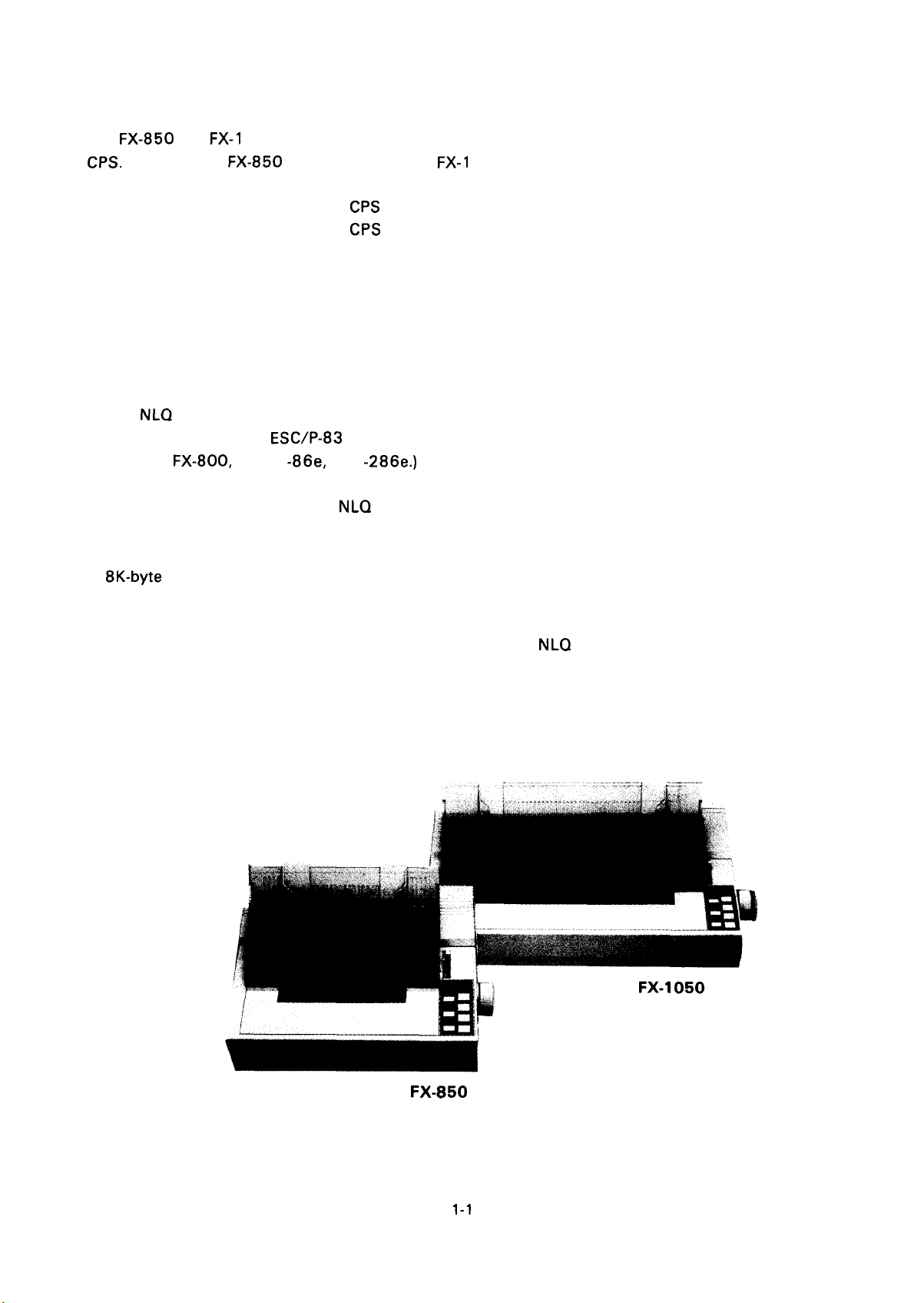
1.1 FEATURES
REV.-A
The FX-850 and
CPS.
Either model FX-850 with 80 columns or
to your requirements. The main features are as follows:
Max. printing speed:
●
Advanced paper handling functions: Auto tear-off
●
●
SelecType function (Any print mode can be selected directly from the front panel). Once a mode is
selected, it is stored in the non-volatile memory, and is selected when the printer power is turned
on.
Two
●
●
●
●
●
●
●
●
●
●
NLQ
Printer driver EPSON
such as
Double-height function
Pitch control is possible in the
Since the IBM emulation mode is standard, these printers are IBM-compatible. The IBM characters
are also standard.
8K-byte
Push tractor unit
Printing is possible on envelopes and labels in addition to fan-fold paper, cut sheets, and roll paper.
User-defined characters are supported in both the Draft and
is registered, it is stored in the non-volatile memory and need not be re-registered. The user-defined
character set can only be selected (as a default character set) using the DIP switches.
Compatible with EPSON optional interface board series #81 XX.
input data buffer (Buffering can be disabled.)
FX-1
050 are serial dot matrix 9-pin terminal
FX-1
050 with
264
CPS
(Draft and Elite)
CPS
220
fonts (Roman and Saris-serif) are standard.
ESC/P-83 is standard. (This driver is compatible with the high class models
FX-800, -1000, -86e, and -286e.)
(Draft and Pica)
Auto loading
Auto back-out
Micro adjustment
NLQ
mode. (Pica, elite, proportional modes)
printers that print at a maximum of 264
136 columns can be selected according
NLQ
(Saris-serif) modes. Once a character
FX-850
Figure 1-1. Exterior Views of the FX-850/1050
1-1
Page 11
REV.-A
No.
Table 1-1. Optional Units
Name
FX-850
FX-1
050
#83 10
#731 1
#731 2
#7339
#7340
#8750
#8755 (M)
#8758
#81 XX Optional Interface Board
Roll Paper Holder
Pull Tractor Unit
Pull Tractor Unit
Cut Sheet Feeder (single-bin)
Cut Sheet Feeder (single-bin)
Ribbon Cartridge
Ribbon Cartridge
Ribbon Pack
Table 1-2. Optional Interface Boards
No.
#8 143 New serial interface
I
o
o
o
o
o
o
o
o
o
Name
I
#8145
I
I
I
I
I
I
#8172 I 32 K-byte buffer parallel interface
I
IRS-232C
#8 148
#8 149 Intelligent serial interface type II
#8 149M Intelligent serial interface type III
#816 1 IEEE-488 interface
#8 165 Intelligent IEEE-488 interface
#81 72M
current loopinterface type II
Intelligent serial interface
128K-byte buffer parallel interface
-., .
t “’
:.
.
1-2
Page 12
1.2 SPECIFICATIONS
REV.-A
The
FX-850/l
specifications for the printer.
1.2.1 Hardware Specifications
Printing Method
Pin Configuration
050 communicates
Serial, impact dot matrix
See Figure 1-2 (diameter: 0.29 mm).
with a wide variety of host computers. This section describes the
Wires
I
# 1’
2
~1
4
51 ‘
7
t
4
T
4
t
i
t
--— --
––-
--
———
0.35mm ( 1/72” )
I
---
0.29mm
---
---
t
Figure 1-2. Printhead Pin Configuration
Feeding Method
NOTES: 1. When using friction feed:
● Use the paper tension unit.
● Do not use fanfold paper.
● Do not perform reverse feed beyond than 1/6 inches after the paper end has been
detected.
● Do not use multi-part, single-sheet forms.
2. When using tractor feed:
●
Release the friction feed mechanism.
●
Multiple copies for printing must be finished by pasting them together at the line or dots.
●
Copy paper must be a carbonless multi-part paper.
a) When using push tractor feed:
Use the paper tension unit.
●
Friction feed
Tractor feed (push: standard, pull: optional)
~1
?
I
1-3
Page 13
REV.-A
● Do not perform reverse feeding for more than 1/6 inches.
● Because accuracy of paper feed cannot be assured, do not perform reverse feeding ‘
after the paper end has been detected.
b) When using pull tractor feed:
● Remove the paper tension unit and mount the pull tractor unit.
● Use the paper path when a single sheet is inserted.
c) When using push-pull tractor feed:
● Remove the paper tension unit and mount the pull tractor unit.
● Do not loosen the paper between the platen and the pull sprocket.
● -Precisely the horizontal position of the pull sprocket and push tractor.
● Do not perform reverse feeding after the paper end has been detected.
Paper Loading Directions
Fanfold paper
Cut sheet paper
Line Spacing
Line Feed Speed See Table 1-3.
Inserted from the rear side
Inserted from the up side
1/6” or programmable (min.
Table 1-3. Line Feed Speeds
f’”
1/2 16“)
Type of Paper Continuous Feed Intermittent Feed Feed Speed
Cut Sheet
Fanfold
Paper Specifications
Cut sheet paper Refer to Table 1-4.
Table 1-4. Cut Sheet Paper Specified Conditions
Width [mm] 182-257 (7.2 - 10.1”) 182-366 (7.2 - 14.4”)
Length
Thickness [mm]
Weight [Kg]
Quality Plain paper
[mm] 182 -
48 ins/line 71 ins/line 3.5 “/see
53 ins/line 76 ins/line
I
I
3.1 “/see
FX-850 FX-1 050
364 (7.2 - 14.3”)
0.065 -
0.10 (0.0025 - 0.004”)
45 - 70 (14 - 22 lb)
f-
..
.
Copies
NOTE: The form overriding mechanism enables printing as close as 13.5 mm from the bottom edge
of the paper. However, paper feed accuracy is not guaranteed within about 22 mm from the
bottom.
Not available
1-4
Page 14
Fanfold
Refer to Table 1-5.
Table 1-5. Fanfold Paper Specified Conditions
Width
Copies
Quality
Total Thickness
Weight
paper
Width
[mm]
[sheet]
[mm]
[Kg]
[mm]
FX-850
- 254 (4.0 - 10.0”) 101 - 406 (4.0 - 16.0”) ~
101
4 (1 original + 3 ) at normal temperature
3 (1 original + 2 ) at all temperature range
Plain paper
0.065 -
Fanfold 45-70 (14 -22 lb)
Multi-part forms 34 - 50 X N (N
Refer to Table 1-6.
Table 1-6. Roll Paper Specifications
I
0.32 (0.0025 -0.01 2“)
s
4)
FX-850
only
FX-1 050
Length
Thickness [mm]
I
Weight [Kg]
Quality
I
Copies
Envelope
Size
Weight
Quality
[mm]
I
I
I
I
Refer to Table 1-7.
Table 1-7. Envelope Specifications
[mm]
[Kg]
Roll diameter not more than 127 mm (5”)
-0.09 (0.0028 - 0.0035”)
0.07
45 - 55
Plain paper
Not available
FX-850/l
166 X 92, 240 X 104
39-
78 (12
Plain, Bond, Air mail
050
-24 lb)
Operating conditions:
Printing must be executed at normal room temperature.
Envelopes must be oriented with the long direction parallel to the carriage.
1-5
Page 15
REV.-A
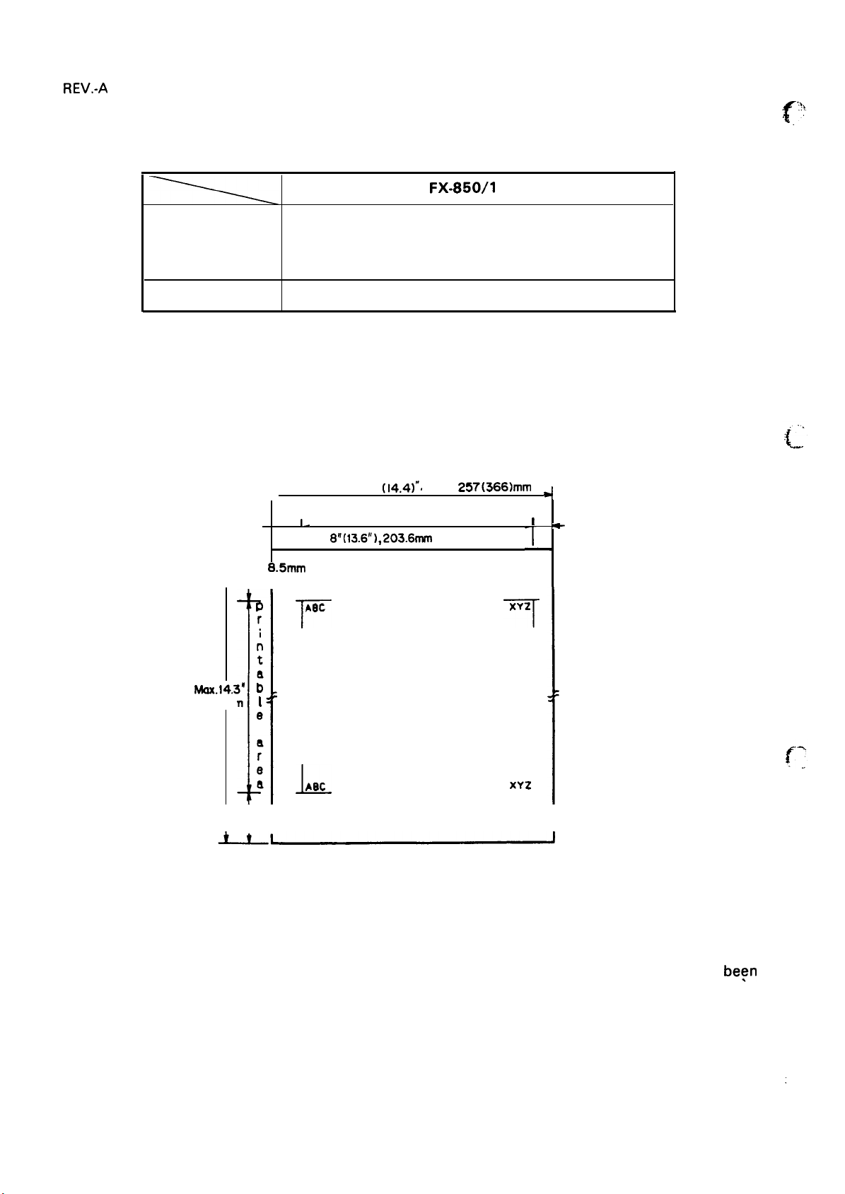
Label
Refer to Table 1-8.
Table 1-8. Label Specifications
f:,,,
.
Size
Thickness [mm]
Printable Area
Cut sheet paper
[mm] 63.5 X 2.38 (2.5 X 15/16”),
0.12”, 3rnm
or more
0.33”,
or more
r
MOX.14.3”
364mm
101.6 X 2.38 (4 X 15/1 6“)
101.6 X 36.5 (4 X 1 7/1 6“)
less than 0.19 (0.0075”)
See Figure 1-3.
10.1*’
(14.4)”.
Printable area
D
r
i
n
t
a
b
I
e
1-
8.5mm
72 -
L
8m(13.6’’),203.6mm
Aec
T
FX-850/l
182 - 257(366)mm
(354.4 mm)
050
T
7
XYZ
-1
I
-
0.12”, 3mm
or more
a
r
e
a
:1
0.87”, 22mm
or more
NOTES: 1. Values in the parentheses apply to the FX-105O.
2. Printing is possible for approximately 42 mm after the bottom edge of a page has
detected. Thus, the value 13.5 mm (lowest print position) is given for reference only. Paper
feed accuracy cannot be assured in the area approximately 22 mm (0.87”) from the bottom
edge of the page.
Figure 1-3. Cut Sheet Paper Printable Area
A8C
1-
1-6
XYZ
-1
1
I
be~n
Page 16
REV.-A
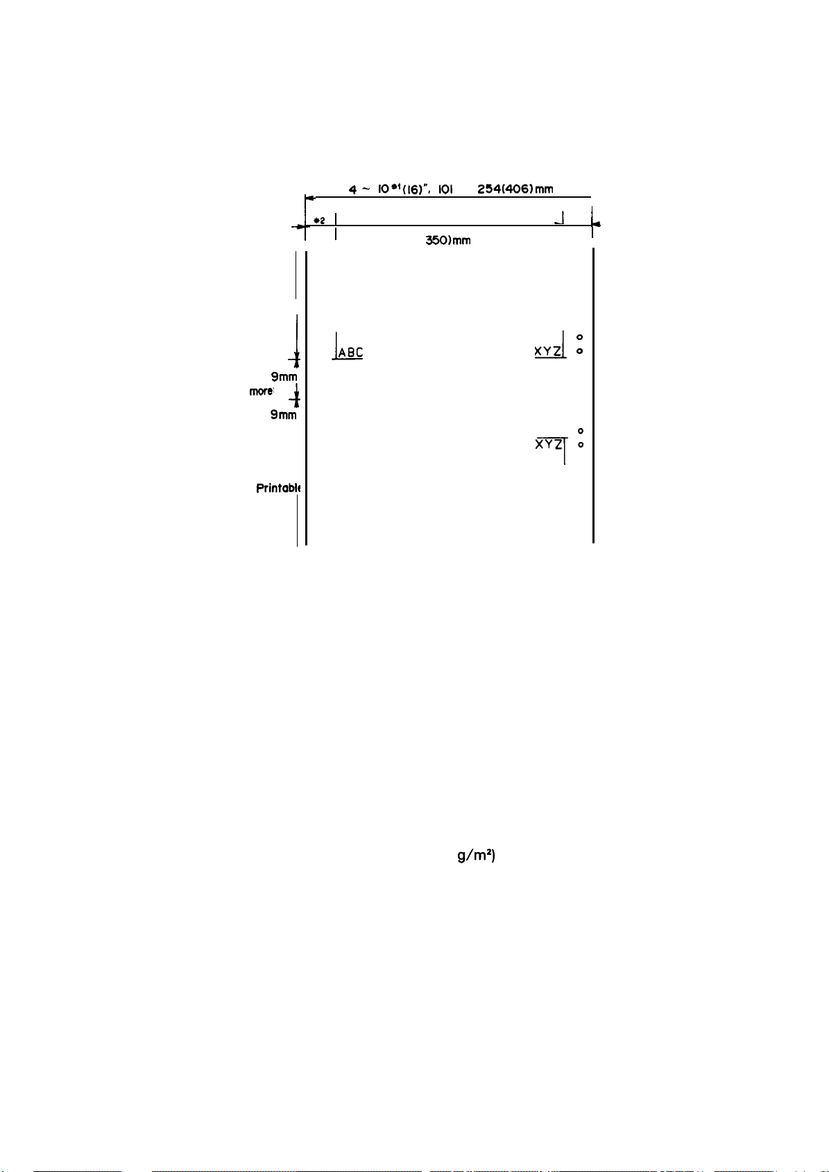
Fanfold paper
Printable
area
0.36”,
or
more!
0.35”,
or more
Printabh
area
See Figure 1-4.
P
1
9mm
4
9mm
4-
*2
o
0
0
0
0
0
0
o ABC
L
o
0
0
---------------------------
o
0
0
o ABC
o
T
o“
i
0
0
0
0
0
10*~(16)”, 101
Printable area
Max. 203.3(
-
350)mm
254(406)mm
,8”(13.8”)
J
XYZ :
J
X’iz :
7
1
*2
~
0
0
0
0
0
0
0
0
0
0
0
0
o
0
0
0
0
0
NOTE: 1. Values in the parentheses apply to FX-105O.
2. 0.47”, 12 mm or more when the 101 to 242 mm (4 to 9.5”) width paper is used.
0.98”, 25 mm or more when the 254 mm (10”) width paper is used.
Figure 1-4. Fanfold Paper Printable Area
Envelopes
Size
Quality
Thickness
No. 6 (166 X 92 mm), No. 10 (240 X 104 mm)
Bond paper, xerographic copier paper, airmail paper
0.16-
0.52 mm (0.0063 -0.01 97”)
NOTE: Differences in thickness within printing area must be less than 0.25 mm (0.0098”).
121
Weight
-241 lb (45 -91
NOTES: 1. Envelope printing is only available at normal temperature.
2. Keep the longer side of the envelope horizontally at setting.
3. Set the left of No. 6 envelope at the setting mark of the sheet guide.
Label
Size
Thickness
2 1/2 X 15/16”, 4 X 15/16”, 4 X 1 7/16”
O.19 mm (0.0075) max.
NOTE: Thickness excluding the base paper must be less than or equal to 0.12 mm (0.0075”).
g\m2)
1-7
Page 17
REV.-A
NOTES: 1.
3.
4.
Printing of labels is only available at
Labels must be fanfold.
2.
Labels with pressure-sensitive paper
and the total thickness must be less
normal temperature.
must be jointed by pasting along the dots or lines,
than or equal to 0.3 mm (O.
under conditions that must be between 5 to 35 “C and 20 to
Examples of labels: AVERY CONTINUOUS FORM LABELS
AVERY MINI-LINE LABELS
11
8“) to be printed out
80Y0
RH.
:!,,
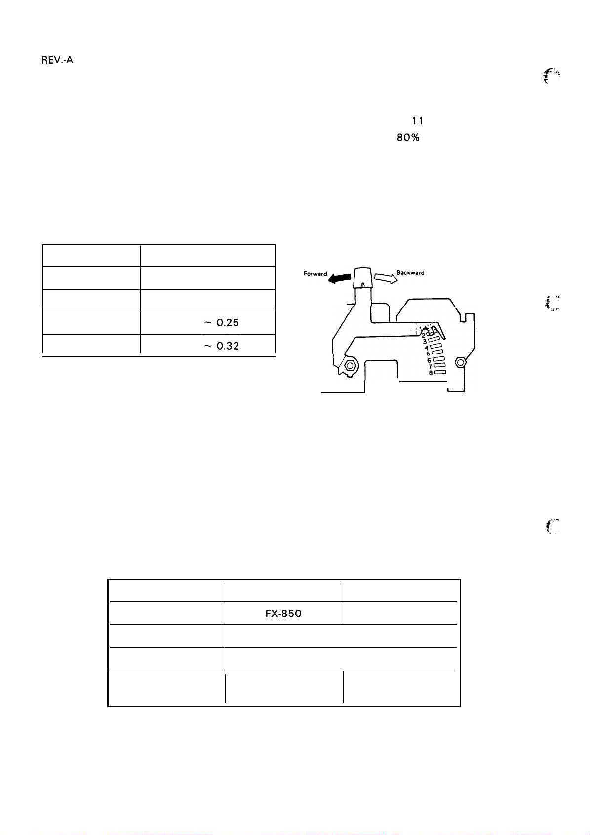
Lever Adjustment
See Figure 1-5 and Table 1-9.
Table 1-9. Lever Adjustment
Lever Position
2nd
3rd
4th
5th
Paper Thickness [mm]
0.06 -0.12
-0.17
o.13
0.18
0.26 .
:::
Head adjustment Lever
‘“’ward-
.fl
(*’
~
q“’’”’”
-~
o
?
~
Figure 1-5.
Head Adjustment Lever
Positioning
NOTES: 1. When printing density becomes lighter, set the head adjustment lever one position lower.
2. When using thicker paper than shown in the above table, set the head adjustment lever
to the 6th or higher appropriate position by performing the self-test operation.
:
.
<=,”
Ribbon Cartridge
Printer
Color
Life
Dimension
(W) X (h) X (d)
See Table 1-10.
Table 1-10. Ribbon
Ribbon Model No.
[characters]
[mm]
Cartridge Specification
#8750
FX-850
3 million (14 dots/character)
293 X 34 X 72
1-8
f-
#8755 (M)
FX-1 050
Black
I
468 X 34 X 78
Page 18
Dimensions
Weight
See Table 1-11 (Details are shown in Figures A-45 and 46.).
See Table 1-11.
Table 1-11. Dimensions and Weight
Width [mm] Height [mm]
FX-850
FX-I 050 605 150
NOTE: Excluding platen knob and paper guide.
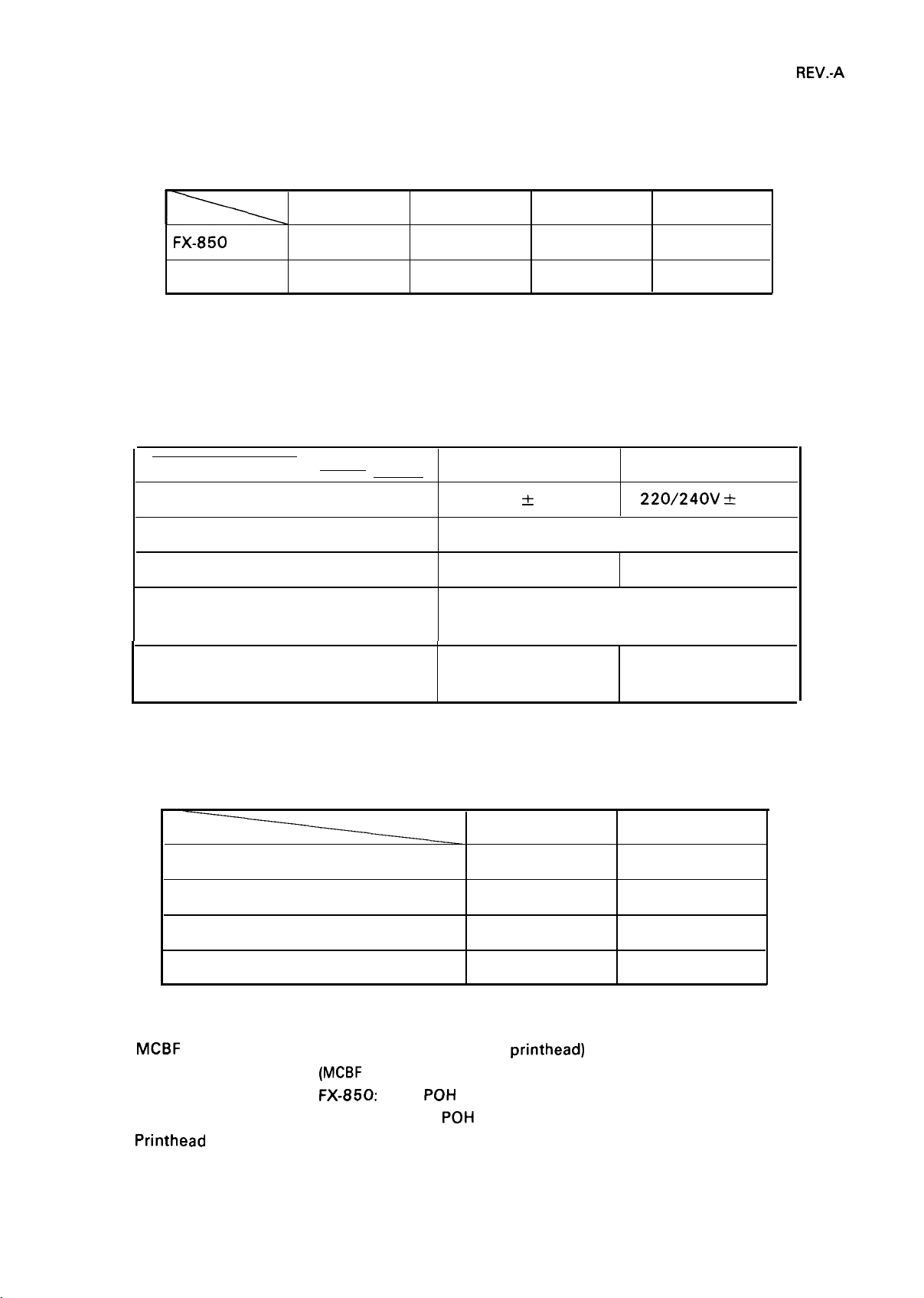
Electrical Specifications See Table 1-12.
—
Voltage [V AC]
Frequency range [Hz] 49.5 - 60.5
Rating current [A]
Insulation resistance [M ohm] min.
(between AC line and chassis)
430 150
Table 1-12. Electrical Specifications
Depth [mm]
120 V Version
*
120V
10YO
2
360
360
Weight [Kg]
9.5
12.5
220/240 V Version
220/240V
10
& 10%
1
Dielectric strength [V AC, rms]
(1 minute, between AC line and chassis)
Environmental Conditions
Temperature [“C]
Humidity [% RH]
Resistance to shock [G] (within 1 ms)
Resistance to vibration [G] (55 Hz, max.)
Reliability
MCBF
MTBF
Printhead
life
1250
Refer to Table 1-13.
Table 1-13. Environmental Conditions
Storage
- 60
–30
- 85
5
2
0.50
5 million lines (excluding
(MCBF
. . .
Mean Cycles Between Failure)
FX-850: 4000
FX-105O: 6000
100 million characters (14 dots/character)
POH
(duty 25%)
POH
printhead)
(duty 25%)
1250
Operating
5 -35
10 - 80
1
0.25
I
1-9
Page 19
REV.-A
Safety Approvals
Safety standards
Radio Frequency
Interference
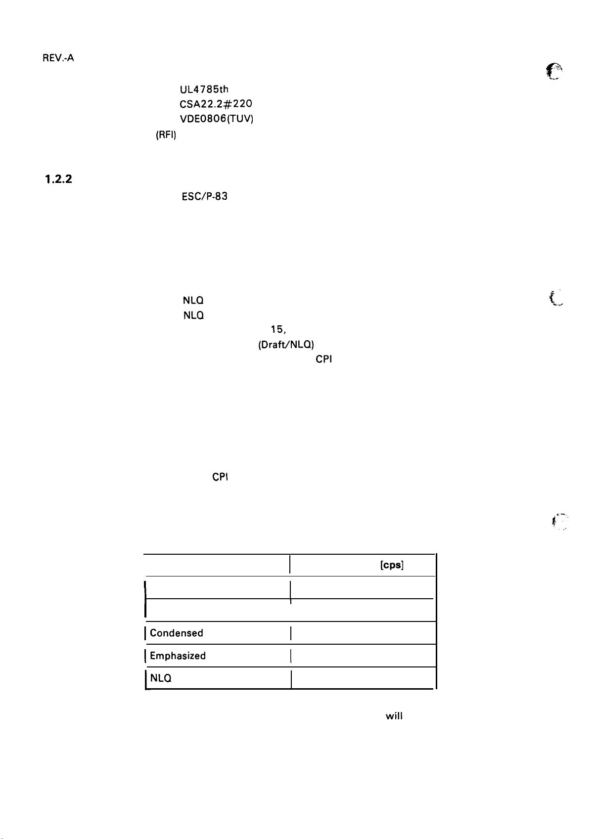
1.2.2
Firmware Specifications
UL4785th (U.S.A. version)
CSA22.2#220
VDE0806
(RFI)
FCC class B (U.S.A. version)
VDE871 (European version)
(TUV)
(European version)
Control Code
Printing Direction
Text
Bit-image
Character Code
Character Set
Font
Printing Mode
NOTE: A condensed mode for 15
ESC/P-83
Bidirectional printing with logic seeking
Unidirectional printing
8 bits
96 ASCII and 13 international character sets
Graphics
NLQ
NLQ
Draft:
Printing quality
Character pitch (10, 12, 15
Roman:
Saris-serif: 10, 12, 15, Proportional
Condensed
Double-width
Double-height
Emphasized
Double-strike
Italic
Underlined
CPI
characters is not available.
10, 12, 15, Proportional
10, 12, 15, Proportional
(Draft/NLQ)
CPI
or Proportional)
Print Speed
I
Draft pica
I
Draft elite
ICondensed draft pica
IEmphasized draft pica
NLQ
NOTE: When any italic character is in the same line, the print speed
the parentheses.
Refer to Table 1-14.
Table 1-14. Print Speed
Type of Letters
normal pica
I
I
I
I
1-10
Print Speed
220 (107)
264 (1 28)
183 (91)
107
45
[CPS]
will be reduced to the value in
Page 20
Print Columns
Refer to Table 1-15.
Table 1-15. Print Columns
Printable Columns
Type of Letters
FX-850
Normal
Condensed
I
Elite
I
Condensed elite 160
NOTE: In Condensed mode, printable column is always 137.
(Previous FX series is 132.)
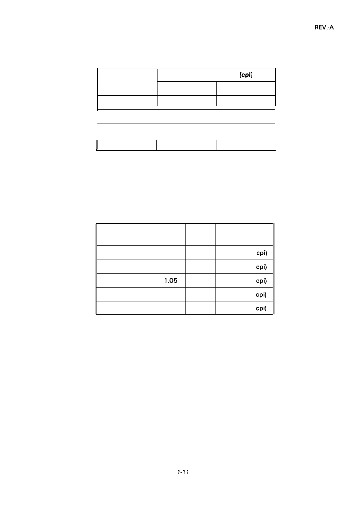
Character Size, Pitch Refer to Table 1-16.
Table 1-16. Character Size and Pitch
Type of Letters
I
I
Width
137
[mm] [mm]
80
96
Height
IcPI]
FX-1 050
136
I
I
Character Pitch
233
163
272
[mm]
I
I
I
Normal
Emphasized
Condensed
Elite 1.7
Condensed elite 0.85
NOTE: Width of Elite character is changed to 1.7 mm from 2.1
mm (not same as normal mode).
2.1
2.1
1.05
3.1
3.1
3.1
3.1
3.1
2.54 (1 O
2.54 (1 O
1.48 (17
2.11 (12
1.27 (20
cpi)
cpi)
cpi)
cpi)
cpi)
1-11
Page 21
REV.-A
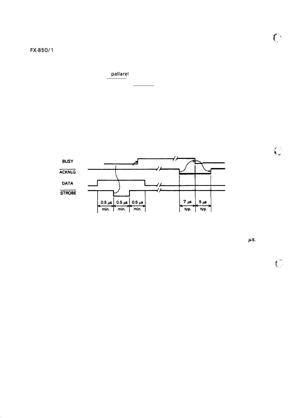
1.3 INTERFACE OVERVIEW
The
FX-850/l
1.3.1 8-bit Parallel Interface Specifications
Data Transmission Mode
Synchronization
Handshaking
Logic Level
Data Transmission Timing
Connector
050 has 8-bit parallel interface as standard.
pallarel
8-bit
By STROBE pulse
By BUSY and ACKNLG (either or both)
TTL compatible
See Figure 1-6.
57-30360 (AMPHENOL) or equivalent
(See Figure 1-7.)
‘“s’
—--J---’
2!-,
=
NOTE: Transmission time (rising and falling time) of every input signal must be less than 0.2
—r—Lrl———ttt—
Figure 1-6. Data Transmission Timing of 8-bit Parallel Interface
ps.
.:.
t,, .
1-12
Page 22
fn
n
-.
s
;
Page 23
REV.-A
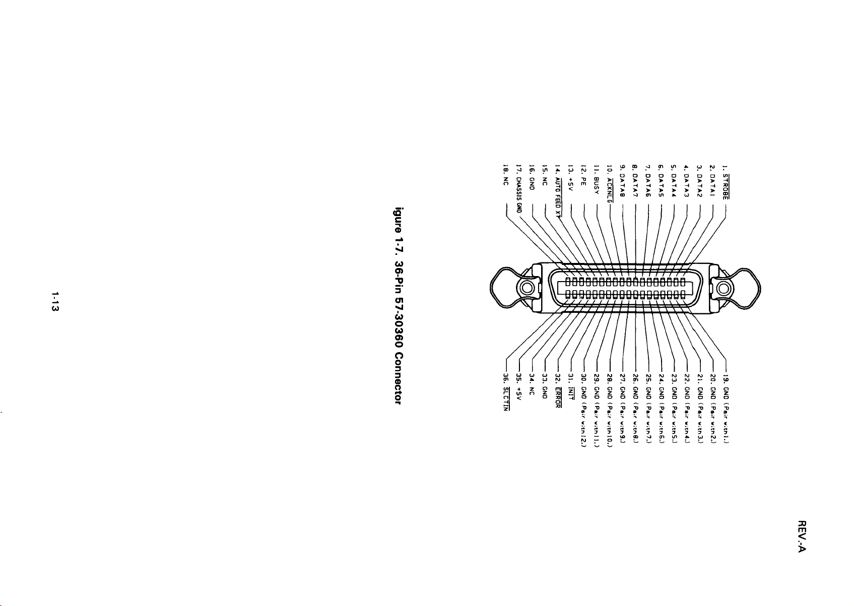
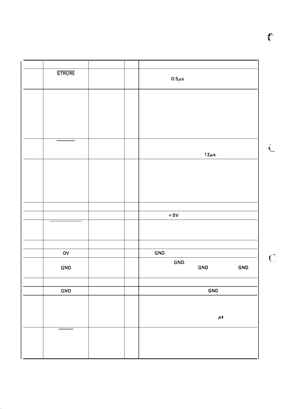
Table 1-17 shows the connector pin assignments and signal functions of the 8-bit parallel interface.
Table 1-17. Connector Pin Assignments and Signal Function
~,.
.., ’
<
Pin No.
1
2
3
4
5
6
7
8
9
10
11
Signal Name
STRORE
DATA 1
DATA 2
DATA 3
DATA 4
DATA 5
DATA 6
DATA 7
DATA 8
ACKNLG
BUSY
Return Pin No.
19
20
21
22
23
24
25
26
27
28
29
DIR
Strobe pulse to read the input data.
In
be more than 0.5#s. Input data is latched after falling
edge of this signal.
These signals represent information of the 1st to 8th
In
In
bits of parallel data, respectively. Each signal is at
“HIGH” level when data is logical “1“ and “LOW” when
In
logical “O”.
In
In
In
In
In
out
This pulse indicates data has been received and the
printer is ready to accept more data.
Pulse width is approximately
out
A “HIGH” signal indicates that the printer cannot
receive data.
ing cases:
1. During data entry
2. During printing operation
3. In off-line status
4. During printer error status
Functional Description
Pulse width must
12#s.
The signal becomes “HIGH” in the follow-
19
12
13
14
15
16
17
18
- 30
31
32
PE
AUTO FEED XT
NC
Ov
CHASSIS
GND
NC
GND
INIT
ERROR
30
out
A “HIGH” signal indicates that the printer is out of paper.
Pulled up to
In
With this signal at “LOW”’ level, the paper is automatically fed one line after printing.
(The signal level can be fixed to “LOW”’ with DIP SW 2-4.)
Not used.
Logic
Printer chassis
In the printer, the chassis
isolated from each other.
Not used.
TWISTED-PAIR RETURN signal
In
When the level of this signal become
GND
+5V
through 3.3 K ohms resistor.
level.
GND.
GND
and the logic
GND
level.
“LOW”, the printer
controller is reset to its initial state and the print buffer
is cleared. This signal is normally at “HIGH” level, and
its pulse width must be more than 50 @ at the receiving
terminal.
out
The level of this signal becomes “LOW” when the
printer is in -
1. Paper-out status
2. Off-line status
3. Error status
GND
are
1-14
Page 24
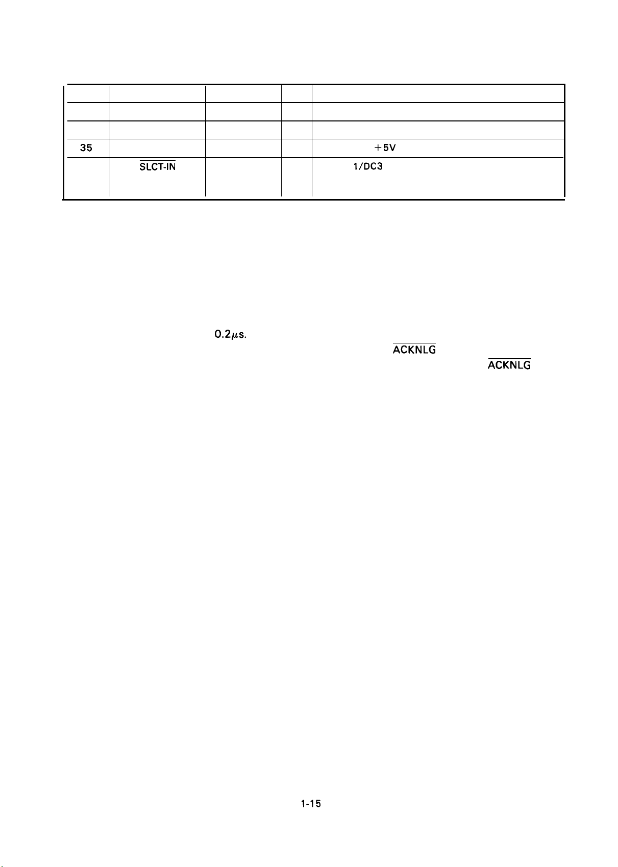
Table 1-17. Connector Pin Assignments and Signal Function (cent’d)
REV.-A
Pin No. Signal Name
33
34
35
36
NOTES: 1.
2.
GND
NC
SLCT-IN
“DIR” refers to the direction of signal flow as viewed from the printer.
“Return” denotes “TWISTED-PAIR RETURN” and is to be connected at signal ground level.
As to the wiring for the interface, be sure to use a twisted-pair cable for each signal and
never fail to complete connection on the Return side. To prevent noise effectively, these
cables should be shielded an connected to the chassis of the host computer and the printer,
respectively.
3.
All interface conditions are based on TTL level. Both the rise and fall times of each signal
must be less than
4.
Data transfer must not be carried out by ignoring the
(Data transfer to this printer can be carried out only after confirming the
or when the level of the BUSY signal is “LOW”.)
Return Pin No.
0.2Ks.
DIR
Functional Description
Same as with Pin No. 19 to 30.
Not used.
Pulled up to
The DC
In
“HIGH” level.
(Internal fixing can be carried out with Jumper- l.)
+5V
through 3.3 K ohms resistor.
l/DC3
code is only valid when this signal is
ACKNLG
or BUSY signal.
ACKNLG
signal
1-15
Page 25
REV.-A
Table 1-18 shows the printer select/deselect (DC
SLCT-IN
input, DC 1
/DC3,
and interface signals.
Table 1-18. Printer Select/Deselect Control
l/DC3)
control, including relations among ON-LINE,
:):>
f
. .
ON-LINE SW
OFF-LINE
ON-LINE HIGH
HIGH/LOW
SLCT-IN
LOW
Dcl/Dc3
DC
l/DC3
DC 1
DC3 HIGH
DC 1
DC3 HIGH
ERROR
LOW HIGH
HIGH
HIGH
LOW\HIGH
(During data
entry)
LOW\HIGH
(During data
entry)
LOW/HIGH
(During data after entry
entry)
LOW/HIGH
(During data
entry)
BUSY
ACKNLG
No pulse Disable
Pulse output
after entry
Pulse output
after entry
Pulse output
Pulse output
after entry
DATA ENTRY
Enable
mal
Enable
(Waits DC1.
See Note 2)
Enable (Nor-
mal
(Nor-
Process)
Process)
NOTES: 1. In the Table 1-18, it is assumed that no ERROR status exists other than that attributable
to OFF-LINE mode.
DC3
2. Once the printer is deselected by the
code, the printer will not revert the selected state
unless the DC 1 code is input again. (In the deselected state, the printer ignores input data
1
until the DC
3. The DC 1 and
code is received.)
DC3
codes are enabled only when the
SLCT-IN
signal (Input Connector No.36
for the parallel interface unit) is HIGH and printer power is initialized.
4. If the
SLCT-IN
signal is LOW when the printer is initialized, DC
l/DC3
printer select/deselect
control is invalidated, and these control codes are ignored.
5. If the
SLCT-IN
signal is HIGH and is not set to LOW by jumper 6 when printer initialized,
the printer starts from the selected (DC 1 ) state.
L
f-:
1-16
Page 26
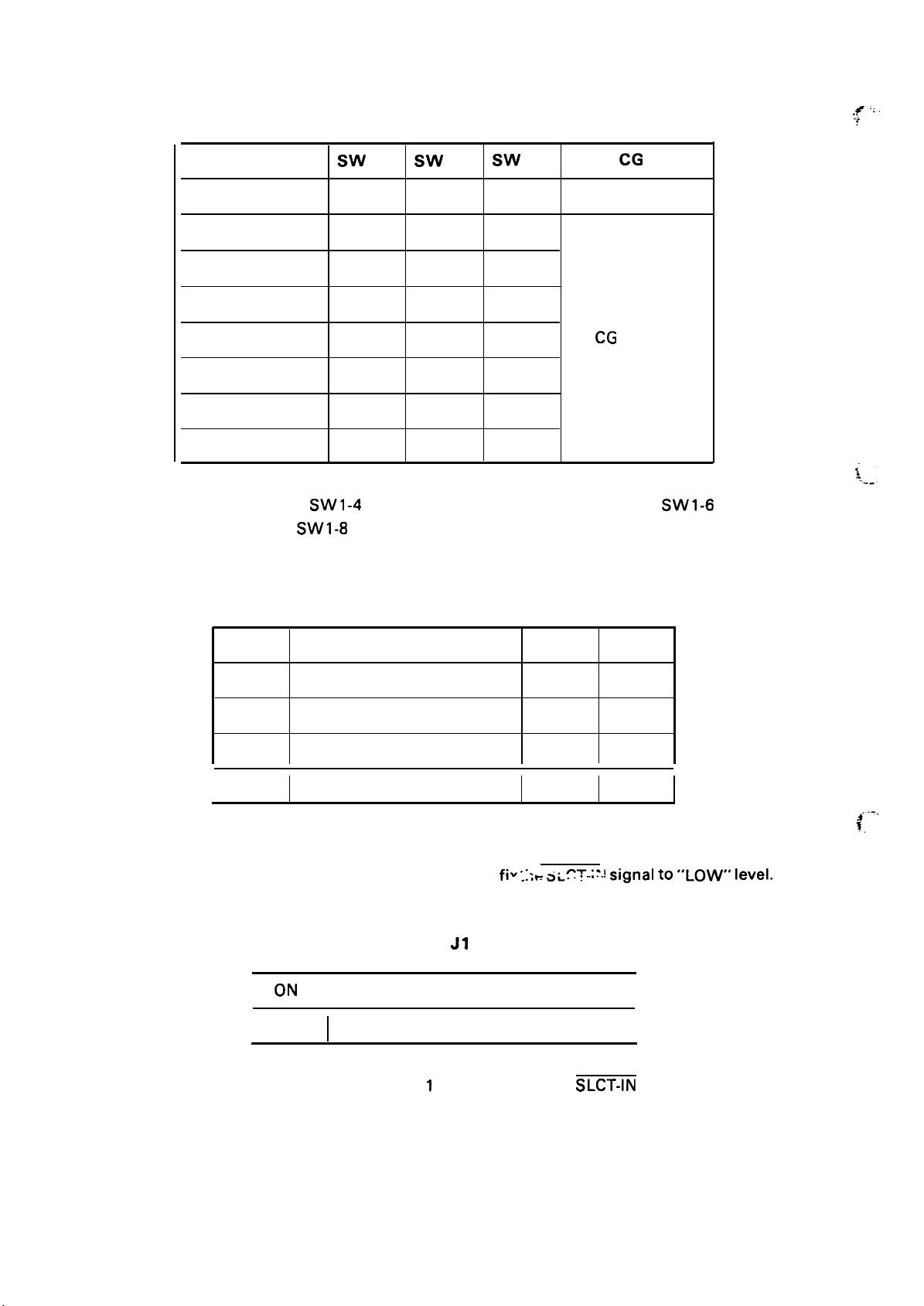
1.4 DIP SWITCHES AND JUMPER SETTINGS
REV.-A
This section describes the DIP switch selections and jumper setting for the
1.4.1 DIP Switch Settings
The DIP switches are located at the right side of the printer. When the printer hardware is initialized,
the following functions are set to the default values shown in the table below.
Table 1-19. DIP Switch 1 Settings
WV
1-1
1-2
1-3
1-4
1-5
1-6
1-7
Description
Default character set
Shape of zero
Table select
Protocol mode
Short tear-off mode
International character set
User-defined
Slashed
Graphic
IBM emulation
off
See Table 1-20.
ON
FX-850/l
OFF
ROM
Not slashed
Italic
ES C/P
On
050 printer.
1-8
NOTE:
Default character set
Shape of zero
Protocol mode
When DIP
When DIP switch 1-1 is ON, the user-defined character set will be selected as default.
User-defined characters are maintained in printer memory even when the power is turned off,
so the user-defined character set can be easily selected simply by turning off the power, setting
this switch to ON, and then turning the power on again.
When DIP switch 1-2 is ON, prints
for clearly distinguishing between
When DIP switch 1-4 is ON, printer operates in the IBM emulation mode; when off, printer
operates in the Epson
Functions of
emulation mode.
SW1-4 is on (IBM mode), the function of DIP SW1-3 changes to auto CR ON/OFF.
a stashed zero (0); when OFF, prints open zeros (0).
uppercase O and zero when printing program lists,
ESC/P mode.
DIP
switches 1-6, 1-7, and 1-8 are different when using the printer in the IBM
Useful
etc.
Short Tear-off
When print operation has finished, the short tear-off feature automatically feeds the perforation
of the continuous paper to the tear-off edge of the sheet guide cover so that the user can tear
off the last sheet. When the user resume printing, the paper is fed backward to the loading
position.
1-17
Page 27
REV.-A
Country
Table 1-20. International Character Set
WV
1-6
SW
1-7
SW
1-8
IBM
CG
Table
,,# ,.
.:
USA
France
Germany
UK ON OFF
Denmark
Sweden
Italy
Spain
NOTE: When DIP SW1-4 is on (IBM mode), the functions of DIP SW1-6
through
SW1-8 change to IBM character generator selection.
ON
ON
ON
OFF
OFF ON
OFF OFF ON
OFF
Table 1-21. DIP Switch 2 Settings
ON
ON
OFF
ON ON
OFF
ON
OFF
ON
OFF
OFF
OFF
CG Table 1
CG
Table 2
Sw
2-1
2-2 Cut sheet feeder mode
2-3
2-4
I
1.4.2 Jumper Setting
The jumper J 1 is located on the main board and it can
I
I
NOTE: If the jumper J 1 is connected, the
Page length
1 -inch skip over perforation
Auto line feed
ON
OFF
signal is fixed to LOW, and DC 1 /DC3 printer
select control is ignored.
Description
Table 1-22. J1 Setting
Fix to “LOW”
Depend on the external signal.
ON
12 inch 11 inch
On
On
On
fiw
;:;-
SLCT-:?-!
SLCT-IN
OFF
off
off
off
signal to “LOW” level.
I
I
,.-,
1.
1-18
Page 28
1.5 SELF TEST OPERATION
The
FX-850/l
● Control Circuit Functions
● Printer Mechanism Functions
● Print Quality
● DIP Switch Settings
Table 1-23 lists the self test operating instructions and Figure 1-8 shows the self test printing.
050 printer has the following self test (self printing) function which checks the following:
Table 1-23. Self Test Operation
REV.-A
Type-face
Draft
NLQ
Start
stop
Turn the power ON while pressing the
LINE FEED switch.
● Paper out condition.
● Press the ON-LINE switch, and turn
Turn the power ON while pressing the
the power OFF.
FORM FEED switch.
MF’12S1
Default character
Shape of zero
CG
Table
Protocol mode
Automatic tear-off
Country
F’age Length
CSF Mode
F“erforation
Skip
fiuto
LF
Input
Buffer
110#57-&.0X +,_
ill’#*~&-OX
“#S%& ’OX+,
#% Z&’ OX+,
5Z&’OX+,-./O1234567 i39:;<=>?@ABCDE FGHIJKLMNOP~RSTUVWXYZ[ \l’’’abcdefdef ghljklmnOpqrstL~ vw~yz{l }
%&’()*+,–./cU234567 s,.,...–.,
&’OX+,-./O134567 E19:;~:=???? @A.SCDEFGHIJKLMNOFRRSTUVWXYZ[\l”” –’abcdefghijklmnOpqrStuvwxy~{i}’”
‘OX+, -./O1234567S9:; <=>?@
-./O134S67E19:;< :=::?
()*+,
)x+,
-./O134567S9:;:; =:}?}? d
O
,
Jl~34567S 9:;<=
/
+,_.
/O12X4S67s9:;<= ;>?
-./0123456789::
-./Ol2S4567S9:;<=> :
ROM
(Unslashed)
o
Italics
ESC/P
Valid
U.S.A. 1-6 ON
11
tich
Invalid
None
Depend on
Valid
=>?@
. . ..-..-,@
:
fN3CDEFGHIJ
@?4r3CDEFGHIJKLKL MNOPQRSTUVWXYZ[\lA
CAEICDEFGHIJKLMNOPQRSTUVWXYZ
I/F
>?@
AECDEFGHIJKLMN0 PQRs
GABCDEFGHIJ
AEICIC DEFGHIJliLMNOPflRSTUVWXYZ[\l”’”-Yabcde fghi.jk.lmnOpqrstuvw~:y
‘@
AECDEFGHIJKLMNOFQRSTUVWXYZ[\l ““-’abcdefgh~JklmnO pqrstLLvw~Y~{
~Bc
DE
FGHIJKL
1–1 OFF
1-2 OFF
1-3
OFF
1-4 OFF
1-5
OFF
1-7
~-~
OFF
2-2
OFF
~-~
OFF
2-4
OFF
KLMNOPQRSTU VWXYZ[’.
MN
OpQRSTUVWXYZ[\],. -’abcdefghijklmn
KLMNOP12RSTUVWXYZ[ \]-’
ON
TuvwxYZ[\]’”’-’
[\l-–Tabcdefghijklmnopqrstuvwxy
1-S ON
abcdefgh IJklmnOPqrstuvw~
]’”
‘abcdefghijklmnopqrstuvwxy
opq
rSt UVWx Y2’[~ }-
‘abcdefghijk.lmnopqrstuvwxy
abcdefghijklmnopqr stuvwx Yz{i}- !“
:
zC}*
Z{ll+ !“
Draft Mode
z
!
!''#$%&-()*+,-./ol23456789:;<=>?@ABcDEFGHIJKLMNoPQRs
!''#$X&-()*+,-./Ol23456789:;c=>?@ABCDEFGHZJKLMNOPQRBTWWKY
-
''#$%&
#$X&-()*
$%&-()*
X&’()*+,-./O123456789 :;C=>?MBCDEFGHIJKLMNOPQRS
&"()*+,-./O123456789 :;C=>?@ABCDEFGHZJKLMNOPQRSTWWKY
‘()*+,
ox+,
)*+,
()&+,
()*
+,-./O123456789 :;<=> ?WBCDEl?GHIJKLMNOFQRSTUVWKYZ[\l
+,-./0123456789 :;<=> ?WBCDEFGHIJKLMNOPQR
+,-./Ofi3456789 :;C=>?@~CDE~~JK~O=~
-./O123458789:;< =>?@ABCDEFGH1JKLMNOPQRS
-./O123456769:; <=>?@ABCDEFGHIJKLMNOFQR
-./012345678g:; <=>?@ABCDE~JKLMN()~S
NLQ
!“#s%&’()*+
!“#s%&’()*+
“tlS%&’OX+, -./O1234567B9:;
#sz&’()*+,-./O1234567
s%& J()*+,
%&’ OX+,
&’(); +,-./O1234567S9:; <=>?@ABCDEFGHIJ
‘08+,
-./O1234S67E9:;< =>?@ABCDEFGHIJ
-./O1234567S9:; <=>?@ABCDEFGHIJ
)*+,
-./01234S67S9:;
,-./O123456789SI< =>?@ABCDEFGHIJ
,-./O123456789:;
-./01234567e9:;<
-./O123456789:;<
<=>7@ABCDEFGHIJKLIINOpQRS
<=>?@
<=>?@
S9:;<=>?@ASCDEFGHIJ
=>?@
fiBCDEFGHIJKLllNOPQRS TUVWXYZ[\ln–’abcde fghijklmnopqrstu VWXY
RBCDEFGHI
=>?@ABCDEFGHIJ KLMNOPQRSTUVWXYZ[ \]”-
IlBCDEFGHIJ
KLMNOPQRSTUVWXYZ[
NLQ
TUVWXYZ[\l’-’abcdef@jkhnn
BTUVWKYZ[\l--’abcdefsMjkhnopqrstuvwxyz{
TWWXYZC\l---abcdef~
(Roman) Mode
KLMNOPQRSTUVWXYZ[
JKLMNOPQRSTUVWXYZ[
KLMNOPQRSTUVWXYZ[
KLMNOP12RSTUVWXYZ[ \] A-’
KLMNOPQRSTUVWXYZ[
KLMNOPQRSTUVWXYZ[
TUVWXYZ[\]A-’abcdef ghijklmnopqrstuvwx Yz{l}+ !“
(Saris-Serif) Mode
TWWXYZ[\:-T’abcdefgMjkhn
Z[\l -
BTWWXYZ[\]”-TabcdefghiJkhn
abcdefghLlklmomrstuvwxy
‘abode
“
Z[\]--’abodefghijklm
TUVWXYZ[\l--’abcdefghijkbn
Z[\l--’abcdefghi@nnomretuvwxyz{l}-
\]A–’abcdefghijk lmnopqrstuvwx
\ln
‘abcdefghti”klmnopqrstuvwxy
\lA-
‘abcdefghijklmnopqrstuvwxyz(
‘abcdefghti”klmnopqrstuvwxyz{;}
● bcdefghti”klmnopqrstuvwxyz{:}-
\]A ‘abcdefghijklmnopqrstuvwxyz{:}+
\l*-%bcdefghti”klmnopqrstu
\]a–’abcdefghijklmnopqr
Figure 1-8. Self Test Printing
1-19
omratuvwx
fghkikhunomrstuwvxyz
opgretuvwxyz{
omrstuvwxyz{!}
opgrstuvwxyz{i}-
omretuwxyz{l}-
!}- !“
!
opgretuvwxyz{j}- !“’
z
VWXYZC}-
stuvwxyz{;
}%
!
!“’
Page 29
REV.-A
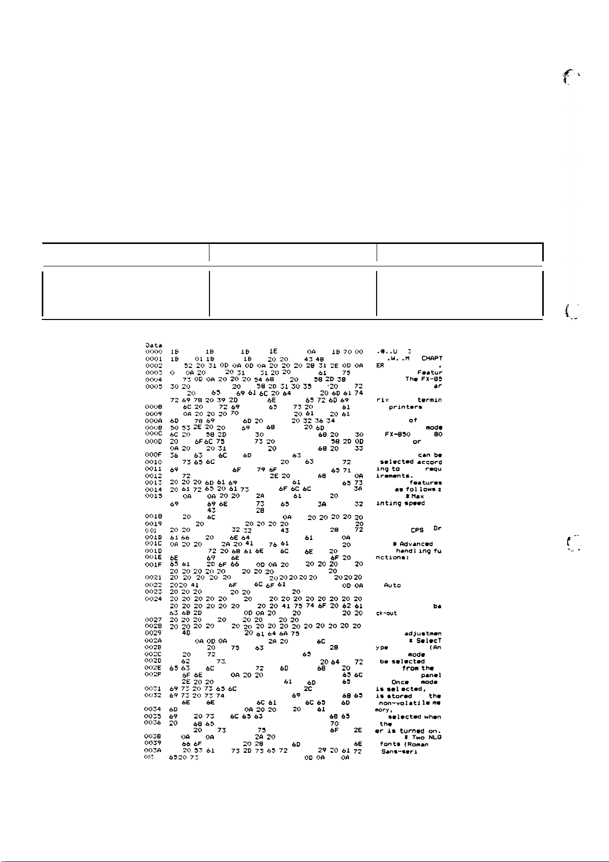
1.6 HEXADECIMAL DUMP FUNCTION
The hexadecimal dump function causes the printer to print the received data in hexadecimal. The printer
prints 16 values in hexadecimal, followed by the corresponding ASCII characters, on one line. If there
is no corresponding printable character for a value (i.e. a control code), a period (.) is printed. Any
remaining data (less than 16 values) can be printed by operating the ON LINE switch. No panel settings
can be made in the hexadecimal dump mode. This function makes it easy for technician to identify
source of communications problems between the printer and computer.
Table 1-24 lists the self test operating instructions and Figure 1-9 shows the hexadecimal dump printing.
Table 1-24. Hexadecimal Dump Operation
the
I
Function Operation
Hexadecimal dump mode
CIata
0,:,0,:,
(:>0(>1
(:)002
0003
00<.,4
,)0(:)5
0006
0007
0008
0009
OOOA
C,ooe
,:,,:,OC
,j(j,jl)
OWE
OOOF
0010
0011
0012
0<113
0014
,:,015
0016
0017
0010
ljo19
,:, C,l
iIOIB
O(>1C
CJOID
Oc:DIE
,>,:,1,=
0020
0021
,:,022
0023
0(>24
0025
0026
,:,027
,5028
0029
OCUA
O(jzn
O02C
OC13J
O(;12E
O02F
0030
0(:,31
0032
0033
CIOT4
0035
0036
0037
CMHB
0039
OO?.la
,>,]y
Turn the power ON while
pressing both the LINE FEED
and FORM FEED switches
Dump Mode
IB 40 00 IB 55 00 IB .33
18 7e 01 IB 57 00
45
S2 20 31 OD
#:,
D
(:,&
20 2,)
6S
7T OD
30
2,>
61 6E 64 20 46 58 2D
&,5
2,:,
73 63 72 b9 61 6C
72 6? 78 20 39 2D 70 69
61
6C 20 70 72 69 6E 74 65 72 73 20 74 68 61 74
OD
OA 20 20 20 70 72 69 6E 74
6D 61 78 69 6D 75 6D 20 6F 66 20 32 36 34 20 4.3
50 53 2E 20 20 45 b? 74 6S 65 72 20 6D 6F 64 65
6C W 46 5S 2D 3S 35
20 63 bF bC 75 6D 6E 77 20 6F 72 20 46 58 2D
OA 20 20 20 31 30 35 30 20 77 69 74 60 20 31 33
36 20 6S 6F 6C 75 6D 6E 73 20 63 61 6E 20 62 65
20
73 65 6C 65 63 74 65 64 20 61 63 63 6F 72 64
b~ 6E 67 20 74 6F 20 79 6F 75 72 20 72 65 71 75
69
72 65 6D 6S 6E 74 73 2E 20 20 S4 68 65 OD OA
20 20 20 6D 61 b9 6E 20 66 65 61 74 73 72 65 73
20 61 72
OD
06 OD OA 20
b9 6E 74 69 6E 67 20 73 70 63 65 64 36 20 20 32
36 34 20
64
20 45 6C 69 74 65 29 OD
20 20
A
El
20
20 20 20 20 20 3Z Z~ 30 20 43 50 53 20 28 44 7Z
61 .% 74 20 61 6E 64 20 50 6? 63 61 29 OD 06 OD
of+
20 20 2,> 2A 20 41 64 76 61 &E 63 65 64 ~o 70
61 70 65
6E 63 74 69 6F 6E 7S 3& 20 20 41 75 74 6F 20 74
6S 61 72 2D 6F 66 66 OD OA 20 20 20 20 20 20 20
20 20 20
20 20 20 20 20 20 20
2<)
20
41 75 74 6F 20 6C 6F 61 64 69 6E 67 oD oA
20 20 20 20 20 20 20 20 20 20 20 20 20 20 20 20
20 20 20 20 20 20 20 20 20 20 20 20 20 20 20 20
~,> ZIJ
20 20 20 ~. 20 20 20 q~ 75 ,4 # 20 62
.53
6B 2D 6F 75 74 OD OR 20 20 20 20 20 20 20 20
20 20 20 20 20 20 20 20 20 20 20 20 20 20 20 20
2(]
20 20
20
4D 69 63 72 6F
74 OD
0~
79 70 65
7?
20 70 72 69 6E 74 20 6D 6F 64 65 20 63 61 6E
20
62 65 20 73 65 6C 6.5 6.3 74 65 64 20 64 69 72
63 63 74 6C 79 20 66 72 6F bD 20 74 60 65 20 66
72
6F 6E 74 OD OA 20 20 20 20 20 70 61 6E 65 6C
29
2E 20 20 4F 6E 6.3 65 20 61 20 6D 6F 64 63 20
b9
7Z 20 7Z 63 6C 65 63 74 69 64 2C 20 &9 74 20
69
77 20 73 74 6F 72 6S 64 20 69 6E 20 74 68 63
20
6E 6F 6E 2D 76 6F 6C 61 74 69 6C 63 20 6D 65
bD 6F 72 79 2C OD 06 20 20 20 20 20 61 6E 64 20
b9
73 20 73 65 6C 65 63 74 65 64 20 77 6B 65 6E
20 74 68 63 20 70 72 69 6E 74 65 72 20 70 6F 77
65 72
20
OD
20
64
b5 20
69 73 20’ 74 75 72 6E 6S 64 20 6F 6E 2E
OA OD
.56
bF 6E 74 73 20 2S 52 6F 6D 61 6E 20 61 6E
20 57 61 6E 73 2D 71 65 72 69 66 29 ~o 61 7Z
7Z 74 61 6E 64 61 72 64 2E OD 06 OD OA 20
oia OD
2,>
31 2E 31
OFI 20 20 20
6!5 2[>
61 77 20 66
2,)
43
50 53 20 2S 44 72 61 66 74 20 61 6E
20 20 20 20 20 20 20 20 20 20 20 20 20
72 20 68 61 6E 64 AC 69 6E 67 20 66 75
21-1 20
20 20 20 20 20 20 20 20 20 20 20
Zf)
20 20 ~o
I>D OA
20 20 20 2A 20 53 65 6C 65 63 54
20 66
7!3
6E 63 74 69 6F 6E 20 20 41 6E
OFI
20 20 20 2A 20 S4 77 6F 20 4E 4C 51
IE 00 OD oA 12
IEI
4D 20 20 20 43 48 41 50 54
OR W 20
54 68 65 20 46 5S 2D 3S .35
?.0
20 77 69 74 68 20 3S
20 20 20 4D 61 78 2E 20 70 72
2!3
20 20
2,>
~1 64 6A 75 73 74 60 65 6E
2!>
2,>
.20 b4
.5E
Z(j 3) 20 20 20
2e 31 2E OD OA
20 4& 65 61 74 75 72
,31
30 35 30
6F 74 20 6D 61 74
20 74 65 72 6D 67 6E
2,>
61 74 20 61 20
.5F 6C
6C 6F 77 73 30
0(4
20 20 20 20 20 20
213 20
Zrj 20 20 20 Zcl
IEI
.20
70 00
61 72
21J 20
20
stop
● Press the ON LINE switch to
set the printer off line. Next,
turn off the printer.
.@.
.U
. .
z
. . . . . .
.x.
.W.
ER
1 . . . . ( 1 . .
. .
1.1
es. .
O ● nd FX-105O ar
e serial dot mat
rix 9-pin termin
● l
printwe
print at ●
. .
maximum of 264 C
Ps .
Either
1
?.0
OD
6.1
FX-850
columns or FX-.
1050 with 13
6 columns
selectmd accord
ing to your
irmmmnts.
main
● ra as fol lows
. . . .
inting speed
64 CPS (
d Elite) . .
220
●
ft and Pica) . . .
* Advancwd
● per handl inq tu
nctions:
ear-off . .
Auto
ck-out
. .
Micro
t
. . . .
YPR function (An
y print
be
swlected
● ctly from th~ f
rent. .
Dnc=
).
is 8Ql Qcted, it
is
stored
no”-volati
mory,
. .
is
soloctmd
thm printer POW
er is
. . . .
fonts (Roman ● n
d
Sans-seri
e standard. . . . .
.M
loading. .
turn-d
CHAPT
Featur
Thm FX-8S
that
mod-
with
can b.
rmqu
Thin. .
features
$
Max . pr
: 2
Draft ● n
CPS
( Dr
auto t
Auto ba
adjustmmn
i SO1OCT
mod-
can
dir
panel
●
mod=
in the
le
● nd
wh.”
o“.
* Two NLQ
f ) ● r
P.
.
80
z
p
ma
f ---
.— -
Figure 1-9. Hexadecimal Dump Printing
1-20
Page 30

REV.-A
1.7 PRINTER INITIALIZATION
There are two initialization methods: hardware initialization and software initialization.
1.7.1 Hardware Initialization
This type of initialization occurs when printer power is turned on or when the printer receives the INIT
signal from the host computer via the 8-bit parallel interface.
When printer is initialized in this way, it performs the following actions:
● Initializes printer mechanism.
● Sets the on-line mode.
● Sets the page length to 11 or 12 inches according to the DIP switch.
● Clears the input data buffer and print buffer.
● Read DIP switch and jumper settings.
● Sets the print mode according to the DIP switch and the non-volatile memory set by control panel.
● Sets printer selections to their default values
1.7.2 Software Initialization
This type of initialization occurs when the printer receives command
(ESC @)
via software.
When the printer is initialized in this way, it performs the following actions:
● Clears the print buffer.
● Sets printer selections to their default values.
NOTE: The printer’s default values are as follows:
Page Position Preset paper position becomes top of form position
Left and Right Margin
Released
Line Spacing 1/6 inches
Vertical Tab Position
Cleared
Horizontal Tab Position Every 8 characters (relative)
VFU Channel Channel O
Family Number of Type Style Roman (Family Number O)
Downloaded Characters Deselected: Software initialize
Cleared:
Hardware initialize
Justification Left justification
Character Per Inch
Bit Image Mode Assignment
Printing Effects
10
ESC
ESC
Z =
Cleared
K =
ESC
ESC
X 3
X O,
ESC
L =
ESC
X 1,
ESC
=
ESC
X 2,
●
1-21
Page 31

REV.-A
1.8 BUZZER OPERATION AND ERROR CONDITIONS
This section describes the buzzer operation and error conditions of the printer.
1.8.1 Buzzer Operation
The buzzer beeps as follows:
●
When a BEL code is sent to the printer, the buzzer sounds for 0.1 second.
When the following error has occured:
●
Carriage Trouble . . . . . . . . . . . . . . . . . . . . .
Paper End . . . . . . . . . . . . . . . . . . . . . . . . . . . . . . . . .
Abnormal Voltage . . . . . . . . . . . . . . . . . . .
RAM Error . . . . . . . . . . . . . . . . . . . . . . . . . . . . . . . . .
Short circuited printhead
drive transistor . . . . . . . . . . . . . . . . . . . . . . . .
●
Recognition of the control panel operation
Beeps once in the following cases:
Self print mode
Hexadecimal dump mode
Print mode setting
●
Proportional space alternation
Beeps once when old proportional space is selected and twice new one is selected.
Beeps 6 times, pausing briefly after 3rd beep.
Beeps 20 times, pausing briefly after every 4 beeps.
Beeps 5 times, pausing every beep.
Beeps 6 to 10 times, pausing briefly after every 2 beeps. The beeps
warn which RAM is incorrect as follows:
6 times . . . . . . . .
8 times . . . . . . . .
10 times . . . . .
Beeps 10 times, pausing after every beep.
Internal RAM (CPU)
Lower Address RAM
Upper Address RAM
(IC)
(IC)
1.8.2
Error Conditions
The printer enters an error state and sets the ERROR signal LOW and BUSY signal HIGH to prohibit
reception of data when any of the following states occurs.
●
The carriage home signal is not detected after the printer mechanism has been initialized (carriage
error).
●
The carriage home position is detected during printing (carriage error).
The printer is set OFF LINE using the ON LINE switch.
●
An internal DC voltage drop is detected (abnormal voltage is detected).
●
●
During initialization, an error is detected by a READ/WRITE check of the RAM in the control circuit.
●
printhead drive transistor is shorted.
A
Interface signal PE is also set HIGH in addition to the above error sequence when any of the following
states occurs.
● The printhead is moved outside of the printable area by a forms override function (paper end state).
● The paper end state continues after the cut sheet feeder mode has been set and paper loading has
been completed (paper end state).
1-22
Page 32

REV.-A
1.9 PAPER HANDLING FUNCTIONS
The push tractor unit can be easily mounted or removed using the paper release lever. Either continuous
paper or cut sheets can be easily selected by operating the LOAD/EJECT switch and paper release lever.
Various paper handling functions are described below.
1.9.1 Autoloading and Backout Function
Loading and ejecting a cut sheet:
When no sheet is loaded, push the paper release lever backward, load the sheet along the sheet guide,
TOF
and press the LOAD/EJECT switch so that the sheet is automatically fed up to the
When the LOAD/EJECT switch is pressed with a sheet loaded, the sheet will be ejected.
Loading and ejecting continuous paper (auto back-out):
Pull the paper release lever forward, load continuous paper onto the push tractor unit, and press the
TOF
LOAD/EJECT switch so that the paper is automatically fed up to the
When the LOAD/EJECT switch is pressed with the paper loaded, the paper is fed in the reverse direction
(ejected) up to the tractor waiting position (auto back-out). If the paper cannot be fed in the reverse
direction at 1/6 inch line spacing, the paper ejection process will be terminated.
position.
position.
1.9.2 Short Tear-Off Function
For continuous paper (when the paper release lever is moved to the tractor feeder side), the paper will
be automatically fed to the perforations (tear-off position) when printing is completed, no data is being
received from the host computer, and the print buffer is empty. At this time, the micro-adjustment
set function becomes valid so that the tear-off position can be adjusted accurately using the LF and
FF switches. The adjusted tear-off position is stored in the memory and remains valid even after the
printer power is turned off, so that the paper will be automatically fed to that position when the tear-off
function is executed later.
After the paper is cut off, the paper is automatically returned to the previous position by sending new
print data or setting the printer OFF LINE.
1.9.3 Micro-Adjustment Top-of-Form Set Function
After paper loading is completed, set the printer ON LINE by pressing the ON LINE switch. In this state,
the paper loading position can be finely adjusted by operating the LF and FF switches. When the printer
is in the micro adjustment mode, the ON LINE LED on the panel blinks. The paper loading position can
be adjusted individually for the friction feed, tractor feed, and cut sheet feeder modes, and the adjusted
values are stored in the memory. The value for the tractor feed remains valid even after the printer power
is turned off.
NOTE: If paper is already loaded when the printer power is turned on, the position of the paper will
TOF
be recognized as the
position.
TOF
1-23
Page 33

REV.-A
1.10 PAPER END DETECTION
The paper end is detected by the PE sensor. When the paper end is detected, the printer indicates it
by lighting the lamp on the control panel and ringing the buzzer. The printer sets the parallel interface
signals
After the paper end is detected, load a new sheet and press the ON LINE switch so that the printer enters
the ON LINE mode. Figure 1-10 shows the paper end detection position.
as shown below, and enters the OFF LINE mode.
● BUSY signal: HIGH
● PE signal:
. ERROR signal: LOW
HIGH
T
Approx.
59. 9mm
I
.-.
ABC
Printable
.------
Paper End Detection
ABC
— —
------------
Area
Posltlon
XYZ
XYZ
1...
---
Fig. 1-10. Paper End Detection Position
1-24
Page 34

1.11 MAIN COMPONENTS
The
FX-850/l
Model-3B 10\3B60 printer mechanism
●
PEGX
●
● PGPNL board (control panel)
PEBFIL-11
●
● Housing
Figure 1-11 shows the
050 printer includes the following major subassemblies:
board (main board)
board (filter board) and power transformer
FX-850/l
050 component locations.
— Power Transformer
FIEV.-A
Pape
Unit
PEBFIL-ll–
Board
r
Tension
Plunger–
Printhead
PEGX
Board
=
Paper Feed Motor
-
Carriage Motor
FX-850
NOTE: In
FX-1 050
FX-850, the paper tension unit and push tractor unit are excluded.
Figure 1-11. Component Locations
1-25
Page 35

REV.-A
1.11.1
The
range of usable paper,
mechanisms are based on printer mechanisms Model-53 10/5360 for the
pull tractor unit or cut sheet feeder can be mounted to the mechanism. Since the construction of these
printer mechanisms are simplified, maintenance is very easy.
Printer Mechanism
Model-3B
10
(FX-850)/3B60 (FX-1
050) are 9-pin dot matrix printer mechanisms, and feature a wide
light weight, compact size, and advanced paper handling function. These
LQ-850/l
050. The optional
F’”
.-,
,.
Figure 1-12.
Figure 1-13.
Model-3B10
Model-3B60
(FX-850)
(FX-105O)
..
.
●
1-26
Page 36

REV.-A
1.11.2 PEGX Board (Main Board)
PEGX
The
board is the main board, and interfaces the printer to the host computer, controls the printer
mechanism and control panel, and supplies DC voltage. Since the complicated logic circuit section is
PEGX
implemented using gate arrays, the
Driver circuits for the motors, sensors, and
on the
Universal
Gate
Memory
PEGX
board are:
IC
STK6722HZ (IC2A)......... . . . . . . . . . . . . . . . . . . . .
●
NJM2355 (lCIA) . . . . . . . . . . . . . . . . . . . . . . . . . . . . . . . . . .
●
Array
E05A15HA (IC3A) . . . . . . . . . . . . . . . . . . . . . . . . . . . . . . . .
●
E05A16GA (IC7A)......... . . . . . . . . . . . . . . . . . . . . . . .
●
IC
●
EP-ROM (IC4A)
●
S-RAM (IC5A and 6A).. . . . . . . . . . . . . . . . . . . . . . . . .
. . . . . . . . . . . . . . . . . . . . . . . . . . . . . . . . . . . . . .
board features very compact construction.
printhead are also included on this board. Other main
Carriage Motor Driver
.
Switching Regulator
Paper Feed and Carriage
and
Printhead
driver
IC
Motors controller,
Host computer interface
Program ROM, 256 K-bit
Buffer and Back up memory
ICS
GA (E05A15HA)
CPU (PPD7810HG)
Figure 1-14.
PEGX
S-RAM (8 KBX2)
%&h
Board
~~
Lithium Battery
GA(E05A16GA)
DIP
DIP
SW2
SW1
1-27
Page 37

REV.-A
1.11.3 PEBFIL-11 Board (Filter Board) and Power Transformer
.K !%
?
The DC power supply circuit is on the main board. The
PEBFIL-11
board and power transformer remove
noise from the AC power supply section and drop the AC input voltage.
Figure 1-15 shows the
PEBFIL-11
board and power transformer.
220/240V
t--
120V
\
220V
(240V)
120V
Figure 1-15.
PEBFIL-11
Board and Power Transformer
1-28
Page 38

REV.-A
1.11.4 PGPNL Board (Control Panel)
LEDs,
There are 11
seven switches, and a buzzer on the control panel. Among these, seven
three switches are for the panel setting function
(SelecType).
Font, character pitch, and condensed mode
LEDs
and
can be selected directly using these switches. Settings set using the SelecType mode are stored in the
memory and are set on the panel when the printer hardware is initialized.
Normally, the SelecType
function is valid when not printing. The printers have various other functions that can be selected from
the control panel.
Figure 1-16 shows the control panel.
Switches
ON LINE
FORM FEED
LINE FEED
Figure 1-16. Control Panel
. . . . . . . . . . . . . . . . . . . . . . . . . . . . . . . . . . . . . . . . . . . . . . . . . . . .
This button controls the printer’s on line/off line status.
When the printer is on
line, ON LINE light is on and the
printer can receive and print data from the computer.
When this lamp is flickering, the micro adjustment
function can be used.
. . . . . . . . . . . . . . . . . . . . . . . . . . . . . . . . . . . . . . . . . . . .
When the printer is off line, press this button to eject a
single sheet of paper or to advance continuous paper to
the top of the next page.
. . . . . . . . . . . . . . . . . . . . . . . . . . . . . . . . . . . . . . . . . . . . . . .
When the printer is off line, press this button to advance
the paper one line, or hold it down to advance the paper
continuously.
1-29
Page 39

REV.-A
LOAD/EJECT . . . . . . . . . . . . . . . . . . . . . . . . . . . . . . . . . . . . . . . . . . . .
This button is used to feed the paper to the loading position,
or to eject paper when paper is already loaded. Paper is
ejected forward if the paper release lever is set to the single
sheet position, and is ejected backward (removed from the
paper path) if the release lever is set to the continuous paper
position.
FONT . . . . . . . . . . . . . . . . . . . . . . . . . . . . . . . . . . . . . . . . . . . . . . . . . . . . . . . . . .
This button is used to select
SERIF, or DRAFT mode. The yellow indicator light shows the
selected font.
PITCH . . . . . . . . . . . . . . . . . . . . . . . . . . . . . . . . . . . . . . . . . . . . . . . . . . . . . . . . .
CONDENSED . . . . . . . . . . . . . . . . . . . . . . . . . . . . . . . . . . . . . . . . . . . .
This button is used to select 10 CPI, 12 CPI, or PS
(proportional) spacing. The yellow indicator light shows the
selected pitch.
This button is used to select or deselect the condensed
mode. The yellow indicator light is on when the printer is
in the condensed mode. In this mode all characters are
printed at approximately 60% of their normal width.
LEDs
POWER (Green) . . . . . . . . . . . . . . . . . . . . . . . . . . . . . . . . . . . . . . . .
READY (Green) . . . . . . . . . . . . . . . . . . . . . . . . . . . . . . . . . . . . . . . . .
On when the POWER switch is on, and power is supplied.
On when the printer is ready to accept input data. This LED
flickers while data is printed.
PAPER OUT (Red) . . . . . . . . . . . . . . . . . . . . . . . . . . . . . . . . . . . .
On when the paper end sensor detects that the printer is
out of paper.
NLQ
ROMAN,
NLQ
SANS-
f
““
;.-
L
. ._.’
!.
I
1-30
!
Page 40

REV.-A
1.11.5 Housing
The housing consists mainly of the upper and lower cases. The components described in the former
sections (1. 11.1 through 1.11 .3) are accommodated in the lower case. Other components are the paper
feed knob, paper separator, and printer cover. The DIP switch position is changed from the rear side
of the printer (conventional) to the right side. A removable cover is located on the upper case so that
the DIP switches on the optional board can be set without removing the upper case.
Figure 1-17 shows the upper and lower cases.
. . . . . . . . . . . . . . . . . . . . . . . . . . . . . . . . . . . . . . . . . . . . . . . .
FX-850
FX-1 050
Figure 1-17. Housing
1-31
Page 41

CHAPTER 2
OPERATING PRINCIPLES
REV.-A
2.1 GENERAL
2.1.1 Cable Connections
2.2 PRINTER MECHANISM OPERATION
2.2.1 Printhead
2.2.2 Carriage Mechanism . . . . . . . . . . . . . . . . . . . . . . . . . . . . . . . . . . . . . . . . . . . . . . . . . . . . . . . . . .
2.2.3 Home Position Sensor . . . . . . . . . . . . . . . . . . . . . . . . . . . . . . . . . . . . . . . . . . . . . . . . . . . . . . . .
2.2.4 Ribbon Feed Mechanism
2.2.5 Paper Feed Mechanism
2.3 CIRCUIT OPERATION
2.3.1 General
2.3.2 Power Supply Circuit
. . . . . . . . . . . . . . . . . . . . . . . . . . . . . . . . . . . . . . . . . . . . . . . . . . . . . . . . . . . . . . . . . . . . . . . . . . . . . . . . . . . . . . . . . . . . . . .
. . . . . . . . . . . . . . . . . . . . . . . . . . . . . . . . . . . . . . . . . . . . . . . . . . . . . . . . . . . . . . .
. . . . . . . . . . . . . . . . . . . . . . . . . . . . . . . . . . . . . . . . . .
. . . . . . . . . . . . . . . . . . . . . . . . . . . . . . . . . . . . . . . . . . . . . . . . . . . . . . . . . . . . . . . . . . . . . . . . . . . . . . . . .
. . . . . . . . . . . . . . . . . . . . . . . . . . . . . . . . . . . . . . . . . . . . . . . . . . . .
. . . . . . . . . . . . . . . . . . . . . . . . . . . . . . . . . . . . . . . . . . . . . . . . . . . . . .
2.2.5.1 Push Tractor Feeding Method . . . . . . . . . . . . . . . . . . . . . . . . 2-8
2.2.5.2 Friciton Feeding Method
. . . . . . . . . . . . . . . . . . . . . . . . . . . . . . . . . . . . . . . . . . . . . . . . . . . . . . . . . . . . . . . . . . . . . . .
Information
2.3.1.1
2.3.1.2
2.3.1.3
2.3.2.1 Filter Circuit
Power Supply Section
Control Circuit Section
Memory Mapping
. . . . . . . . . . . . . . . . . . . . . . . . . . . . . . . . . . . . . . . . . . . . . . . . . . . . . . . . . . . . .
. . . . . . . . . . . . . . . . . . . . . . . . . . . . . . . . . . . . . . . . . . . . . . . .
. . . . . . . . . . . . . . . . . . . . . . . . . . . . . . . . . . . . . . . . . . . . . . . . . . . . . . . . . .
. . . . . . . . . . . . . . . . . . . . . . . . . . . . . . . . . . . . . . . . . . . . . . . . . . . . . . . . .
. . . . . . . . . . . . . . . . . . . . . . . . . . . . . . . . . .
. . . . . . . . . . . . . . . . . . . . . . . . . . . . . . . . . . . . . . .
. . . . . . . . . . . . . . . . . . . . . . . . . . . . . . . . . . . . .
2-1
2-1
2-3
2-4
.
2-5
.
2-5
2-6
2-7
2-9
2-10
2-1o
2-1o
2-12
2-14
2-15
2-1 e
2.3.2.2 Transformer
2.3.2.3 Rectifier and Smoothing Circuit . . . . . . . . . . . . . . . . . . . . 2-17
2.3.2.4 Chopper-Type Switching
Regulator Circuit
2.3.2.5 Pulse-Width Modulation
+5V
2.3.2.6
2.3.2.7
2.3.2.8 + 12V DC Supply Circuit
2.3.2.9 Vx Voltage Supply Circuit
2.3.3 Main
2.3.4 Main Circuit Operation
IC Function
2.3.3.1 CPU Functions
2.3.3.2 E05A15HA Gate Array Functions ................ 2-29
2.3.3.3 E05A16GA Gate Array Functions ................ 2-31
2.3.4.1 Reset Circuit
2.3.4.2 Interface Control Circuit
2.3.4.3 DIP Switch Circuit and Jumpers .................. 2-37
Regulator Circuit
+24V
Regulator Circuit
. . . . . . . . . . . . . . . . . . . . . . . . . . . . . . . . . . . . . . . . . . . . . . . . . . . . . . . . . . . . . . . . . .
. . . . . . . . . . . . . . . . . . . . . . . . . . . . . . . . . . . . . . . . . . . . . . . . . . . . . . . . . .
. . . . . . . . . . . . . . . . . . . . . . . . . . . . . . . . . . . . . . . . . . . . . . . . .
(PWM)
. . . . . . . . . . . . . . . . . . . . . . . . . . . . . . . . . . . . . .
. . . . . . . . . . . . . . . . . . . . . . . . . . . . . . . . . . .
. . . . . . . . . . . . . . . . . . . . . . . . . . . . . . . . . . . . . . . . . . . . . . . . . . . . .
. . . . . . . . . . . . . . . . . . . . . . . . . . . . . . . . . . . . . . . . . . . . . . . . . . . . . . .
. . . . . . . . . . . . . . . . . . . . . . . . . . . . . . . . . . . . . . . . . . . . . . . . . . . . . . . . .
. . . . . . . . . . . . . . . . . . . . . . . . . . . . . . . . . .
Circuit ..... 2-19
. . . . . . . . . . . . . . . . . . . . . . . . . . . . . . . . .
. . . . . . . . . . . . . . . . . . . . . . . . . . . . . . .
2-16
2-18
2-21
2-23
2-25
2-26
2-27
2-27
2-33
2-33
2-34
2.3.4.4 Memory Back-up Circuit
2-i
. . . . . . . . . . . . . . . . . . . . . . . . . . . . . . . . . .
2-38
Page 42

REV.-A
2.3.4.5 Printer Error Detection . . . . . . . . . . . . . . . . . . . . . . . . . . . . . . . . . . . . . 2-39
2.3.5 Printer Mechanism Control . . . . . . . . . . . . . . . . . . . . . . . . . . . . . . . . . . . . . . . . . . . . . . . 2-41
2.3.5.1 Carriage Control Circuit . . . . . . . . . . . . . . . . . . . . . . . . . . . . . . . . . . . 2-41
2.3.5.2 Carriage Motor Software Control ................. 2-49
2.3.5.3 Paper Feed Control Circuit
2.3.5.4 Plunger Drive Circuit . . . . . . . . . . . . . . . . . . . . . . . . . . . . . . . . . . . . . . . . . 2-58
2.3.5.5 Printhead Control Circuit
. . . . . . . . . . . . . . . . . . . . . . . . . . . . . .
. . . . . . . . . . . . . . . . . . . . . . . . . . . . . . . .
2-53
2-60
LIST OF FIGURES
Figure 2-1.
Figure 2-2.
Figure 2-3.
Figure 2-4. Carriage Mechanism
Figure 2-5.
Figure 2-6.
Figure 2-7.
Figure 2-8.
Figure 2-9. Control Circuit Block Diagram
Figure 2-10. Memory Mapping
Figure 2-11.
Figure 2-12. Transformer Circuit
Figure 2-13. Rectifier and Smoothing Circuit
Figure 2-14. Step-Down Circuit
Figure 2-15. Step-Down Timings
Figure 2-16. NJ M2355 Internal Circuit
Figure 2-17. Output Transistor Drive Waveform . . . . . . . . . . . . . . . . . . . . . . . . . . . . . . . 2-20
Cable Connections
Print Mechanism Block Diagram
Printhead Mechanism
Ribbon Feed Mechanism
Push Tractor Feeding Method
Friction Feeding Method
Power Supply Block Diagram . . . . . . . . . . . . . . . . . . . . . . . . . . . . . . . . . . . . . . . . . . 2-10
PEBFIL-11
Filter Circuit Board
. . . . . . . . . . . . . . . . . . . . . . . . . . . . . . . . . . . . . . . . . . . . . . . . . . . . . . . . . . . . . . .
. . . . . . . . . . . . . . . . . . . . . . . . . . . . . . . . . . .
. . . . . . . . . . . . . . . . . . . . . . . . . . . . . . . . . . . . . . . . . . . . . . . . . . . . . . . .
. . . . . . . . . . . . . . . . . . . . . . . . . . . . . . . . . . . . . . . . . . . . . . . . . . . . . . . . . . .
. . . . . . . . . . . . . . . . . . . . . . . . . . . . . . . . . . . . . . . . . . . . . . . . . . .
. . . . . . . . . . . . . . . . . . . . . . . . . . . . . . . . . . . . . . . . .
. . . . . . . . . . . . . . . . . . . . . . . . . . . . . . . . . . . . . . . . . . . . . . . . . . . .
. . . . . . . . . . . . . . . . . . . . . . . . . . . . . . . . . . . . . . . .
. . . . . . . . . . . . . . . . . . . . . . . . . . . . . . . . . . . . . . . . . . . . . . . . . . . . . . . . . . . . . . . . .
. . . . . . . . . . . . . . . . . . . . . . . . . . . . . . . . . . . . . . . . . . .
. . . . . . . . . . . . . . . . . . . . . . . . . . . . . . . . . . . . . . . . . . . . . . . . . . . . . . . . . . . . .
. . . . . . . . . . . . . . . . . . . . . . . . . . . . . . . . . . . . .
. . . . . . . . . . . . . . . . . . . . . . . . . . . . . . . . . . . . . . . . . . . . . . . . . . . . . . . . . . . . . . .
. . . . . . . . . . . . . . . . . . . . . . . . . . . . . . . . . . . . . . . . . . . . . . . . . . . . . . . . . . . . .
. . . . . . . . . . . . . . . . . . . . . . . . . . . . . . . . . . . . . . . . . . . . . . . .
2-1
2-3
2-4
2-5
2-6
2-8
2-9
2-12
2-14
2-16
2-16
2-17
2-18
2-18
2-19
Figure 2-18.
Figure 2-19. Oscillator Waveform . . . . . . . . . . . . . . . . . . . . . . . . . . . . . . . . . . . . . . . . . . . . . . . . . . . . . . . . . . . 2-21
Figure 2-20. Constant-Voltage Control
Figure 2-21. AMP 1 Output
Figure 2-22..
Figure 2-23. Constant-Voltage Control
Figure 2-24. Over-Current Protection (OCP)
Figure 2-25. + 12V DC Circuit . . . . . . . . . . . . . . . . . . . . . . . . . . . . . . . . . . . . . . . . . . . . . . . . . . . . . . . . . . . . . . . . . 2-25
Figure 2-26. Vx Voltage Circuit
Figure 2-27. Reset Circuit . . . . . . . . . . . . . . . . . . . . . . . . . . . . . . . . . . . . . . . . . . . . . . . . . . . . . . . . . . . . . . . . . . . . . . . . . . 2.33
Figure 2-28. Interface Control Circuit Block Diagram . . . . . . . . . . . . . . . . . . . . . 2-34
+5V
Regulator Circuit
+24V
Regulator Circuit
. . . . . . . . . . . . . . . . . . . . . . . . . . . . . . . . . . . . . . . . . . . . . . . . . . . . . . . . . . . . . . . . . . . . . . .
. . . . . . . . . . . . . . . . . . . . . . . . . . . . . . . . . . . . . . . . . . . . . . . . . . . . . . .
(+5V
. . . . . . . . . . . . . . . . . . . . . . . . . . . . . . . . . . . . . . . . . . . . . . . . . . . .
(+24V
DC) . . . . . . . . . . . . . . . . . . . . . . . . . . 2-24
. . . . . . . . . . . . . . . . . . . . . . . . . . . . . . . . . . . . . . . . . . . . . . . . . . . . . . . . . . . . . . .
Z.ii
. . . . . . . . . . . . . . . . . . . . . . . . . . . . .
DC)
. . . . . . . . . . . . . . . . . . . . . . . . . . . . . . . . . . . . . . . .
2-21
2-22
2-22
2-23
2-24
2-26
Page 43

REV.-A
!
Figure 2-29. Data Transmission Timing
Figure 2-30. Serial Data Flow
Figure 2-31. DIP Switch Circuit . . . . . . . . . . . . . . . . . . . . . . . . . . . . . . . . . . . . . . . . . . . . . . . . . . . . . . . . . . . . .
Figure 2-32. Memory Back-up Circuit
Figure 2-33. Carriage Motor Control Block Diagram . . . . . . . . . . . . . . . . . . . . . . . 2-41
Figure 2-34. GA(E05A15HA) Operation Diagram . . . . . . . . . . . . . . . . . . . . . . . . . . . . . . 2-42
Figure 2-35. GA(E05A16GA) Operation Diagram
Figure 2-36. Carriage Motor Drive Circuit Block Diagram ............. 2-44
Figure 2-37. Carriage Motor Drive Sequence
Figure 2-38. Carriage Motor Drive Circuit Block Diagram ............. 2-47
Figure 2-39. Carriage Motor Control Circuit
Figure 2-40. High Speed Skip Operation . . . . . . . . . . . . . . . . . . . . . . . . . . . . . . . . . . . . . . . . . . . . . . 2-50
Figure 2-41. Home Position Seek Operation
Figure 2-42. Home Position Seek Phase States . . . . . . . . . . . . . . . . . . . . . . . . . . . . . . . . . 2-52
Figure 2-43. Paper Feed Motor Drive Circuit Block Diagram . . . . . . . 2-53
Figure 2-44. GA(E05A15HA) Function for Paper Feed Motor ....... 2-54
Figure 2-45. Phase Excitation System . . . . . . . . . . . . . . . . . . . . . . . . . . . . . . . . . . . . . . . . . . . . . . . . . .
Figure 2-46. Paper Loading/Ejecting Operation
Figure 2-47. Plunger Mechanism
. . . . . . . . . . . . . . . . . . . . . . . . . . . . . . . . . . . . . . . . . . . . . . . . . . . . . . . . . . . . . . . . . . .
. . . . . . . . . . . . . . . . . . . . . . . . . . . . . . . . . . . . . . . . . . . . . . . . . . . . . . . . . . . .
. . . . . . . . . . . . . . . . . . . . . . . . . . . . . . . . . . . . . . . . . . . . . . . .
. . . . . . . . . . . . . . . . . . . . . . . . . . . . . . . . . . . . . . . . . . . . . . . . . . . .
. . . . . . . . . . . . . . . . . . . . . . . . . . . . . .
. . . . . . . . . . . . . . . . . . . . . . . . . . . . . . . . . . . . .
. . . . . . . . . . . . . . . . . . . . . . . . . . . . . . . . . . . . . . .
. . . . . . . . . . . . . . . . . . . . . . . . . . . . . . . . . . . . . . .
. . . . . . . . . . . . . . . . . . . . . . . . . . . . . . . . .
2-35
2-36
.
2-37
2-38
2-43
2-45
2-48
2-51
.
2-54
2-57
2-58
Figure 2-48. Plunger Drive Circuit
Figure 2-49. Relationship Between Transistors and Plunger ........ 2-59
Figure 2-50. Printhead Central Circuit Block Diagram ................... 2-60
Figure 2-51. Print Drive Pulse Width
Figure 2-52. Half-dot Protection Circuit
. . . . . . . . . . . . . . . . . . . . . . . . . . . . . . . . . . . . . . . . . . . . . . . . . . . . . . . . . .
. . . . . . . . . . . . . . . . . . . . . . . . . . . . . . . . . . . . . . . . . . . . . . . . . . . .
. . . . . . . . . . . . . . . . . . . . . . . . . . . . . . . . . . . . . . . . . . . . . . . .
2-58
2-61
2-62
LIST OF TABLES
Table 2-1.
Table 2-2.
Table 2-3.
Table 2-4.
Table 2-5.
Table 2-6.
Table 2-7.
Table 2-8.
Board Connector Summary
Power Supply Application
Pin Function of CPU
Pin Function fo GA(E05A15HA)
Pin Function of
ST-RAM Conditions
2-2 phase Excitation
1-2 phase Excitation . . . . . . . . . . . . . . . . . . . . . . . . . . . . . . . . . . . . . . . . . . . . . . . . . . . . . . . . . .
GA(E05A16GA)
. . . . . . . . . . . . . . . . . . . . . . . . . . . . . . . . . . . . . . . . . . . . . . . . . . . . . . . . . . .
. . . . . . . . . . . . . . . . . . . . . . . . . . . . . . . . . . . . . . . . . . . . . . . . . . . . . . . . . . . . .
. . . . . . . . . . . . . . . . . . . . . . . . . . . . . . . . . . . . . . . . . . . . . . . . . . . . . . . . . . .
. . . . . . . . . . . . . . . . . . . . . . . . . . . . . . . . . . . . . . . . . . . . . .
. . . . . . . . . . . . . . . . . . . . . . . . . . . . . . . . . . . . . . . . . . . . . . . . .
. . . . . . . . . . . . . . . . . . . . . . . . . . . . . . . . . . . . .
. . . . . . . . . . . . . . . . . . . . . . . . . . . . . . . . . . . . . 2-31
2-2
2-11
2-27
2-29
2-38
2-46
.
2-46
Table 2-9.
Table 2-10.
Table 2-11.
Carriage Speed Modes
Acceleration/Deceleration Control . . . . . . . . . . . . . . . . . . . . . . . . . . . . . . . . 2-49
2-2 phase Excitation
. . . . . . . . . . . . . . . . . . . . . . . . . . . . . . . . . . . . . . . . . . . . . . . . . . . . . . .
. . . . . . . . . . . . . . . . . . . . . . . .
2-iii
.
. . . . . . . . . . . . . . . . . . . . . . . . .
. ,,,,,,,,
2-49
2-55
Page 44

REV.-A
Table 2-12. Paper Feed Motor Speed
. . . . . . . . . . . . . . . . . . . . . . . . . . . . . . . . . . . . . . . . . . . . . . . . . . .
Table 2-13. Paper Feed Direction and Operation
. . . . . . . . . . . . . . . . . . . . . . . . . . . . .
2-55
2-55
Table 2-14. Acceleration/Deceleration Mode . . . . . . . . . . . . . . . . . . . . . . . . . . . . . . . . . . . . 2-56
Table 2-15. Relationship Between GA Ports and
piunger Voltage
. . . . . . . . . . . . . . . . . . . . . . . . . . . . . . . . . . . . . . . . . . . . . . . . . . . . . . . . . . . . . . . . . . .
.
2-59
.Q
2-iv
Page 45

REV.-A
2.1 GENERAL
This chapter describes the operation of each component. Section 2.2 and the subsequent sections give
more detailed descriptions of each component.
2.1.1 Cable Connections
PEGX
The printer components are connected to and controlled by the
interconnection of the components.
board. Figure 2-1 shows the
Power
Transformer
120V
220V
240V
&
/>
PEGFLU
board
120V
220/240V
LL
I
f
1
Model-3Bl O/3B60
PEGX
board
I
PGPNL
board
<
(c%%’)
AC120V
AC220V
AC240V
/
Host computer
Figure 2-1. Cable Connections
‘
2-1
Page 46

REV.-A
Each component is connected to one of the connectors on the
2-1. Table 2-1 describes the connectors.
Table 2-1 Board Connector Summary
PEGX
board, which are listed in Table
“:,
c
Circuit
Board
PEGX
board
Connector
Number
CN 1
CN2
CN3
CN4
CN5
CN6
CN7
Description
Standard 8-bit parallel interface connector.
Used for data transfer from the host computer.
Connector for the optional interface board. Used
for data transfer from the host computer. When
the optional interface board is mounted, CN 1 is
invalid.
Supplies two step-down AC voltages from the
power supply transformer to the DC regulator
circuit on the
Drives the printhead needles.
Drives the plunger that opens and shuts the
paper bail on the printer mechanism.
Transfers the state of the carriage home position
sensor from the printer mechanism to the control circuit on the
Transfers the state of the paper end sensor from
the printer mechanism to the control circuit on
the
PEGX
PEGX
board.
board.
PEGX
board.
Number
of Pins
36
26
4
12 Table A-1 8
2
3
2
Reference
Table
Table A-1 5
Table A-1 6
Table A-1 7
Table A-1 9
Table A-20
Table A-2 1
‘(,.’
CN8
CN9
CN 10
CN 11
Drives the paper feed motor.
Drives the carriage motor.
Transfers the state of the release lever from the
printer mechanism to the control circuit on the
PEGX
board.
Interface connector between the
and the control panel.
PEGX
board
6
9
2
20 Table A-25
Table A-22
Table A-23
Table A-24
2-2
Page 47

REV.-A
2.2 PRINTER MECHANISM OPERATION
The printer mechanism is a 9-pin serial dot matrix impact mechanism. Figure 2-2 shows a drawing of
the mechanism. The name in the rectangles indicate relationship between each mechanism and the
control circuit on the PEGX board.
E05A15HA
CN7
Plunger
Ribbon
Feed
E05A15HA
u
Paper End
/
v“’’’’” “’”
I
)Kl
Home Position
CN6
Figure 2-2. Printer Mechanism Block Diagram
Sensor
Platen
‘r““
+
Printhead
Drive
Circuit
----
“ ‘ “ ‘
+
E05A15HA
D
““I
(O
Carriage Motor
Control
Circuit
Carriage Motor
Cantrol
Circuit
Feed Motor
The printer mechanism is composed of the following:
Printhead
●
● Carriage Mechanism
● Home Position Sensor
● Ribbon Feed Mechanism
● Paper Feed Mechanism
2-3
Page 48

REV.-A
2.2.1 Printhead
The printhead is an electromagnetic induction 9-pin serial dot head. Nine dot wires are driven
individually to print a dot pattern on the paper, positioned between the platen and ribbon, by hitting
the ink ribbon against the paper and the platen. Print data expanded on the PEGX board is converted
into dot-image data for one vertical row, and output to the
printhead by the printhead drive circuit. A
character is printed by serially printing the dot patterns for each vertical row in the horizontal direction
as the carriage moves. Figure 2-3 shows the
Dot Wire
W~re Reaettmg
Stopper
Spring
printhead mechanism
Ribbon
Platen
Mask
P-~,
*
*,.
Actuating Plate Spring
Figure 2-3. Printhead Mechanism
Paper
2-4
Page 49

REV.-A
2.2.2 Carria9e Mechanism
the
The carria9e is driven by the carria9e motor via a timin9 belt, and moves left and right alon9 the platen.
Since a stepPer motor is used for the
position.
The carriage motor is controlled by a
carria9e motor,
very simPle, oPen-lOOp sYstem-
carria9e can be stopped and started at any
Figure 2-4 shows the carria9e mechanism.
Carria9e Mechanism
2.2.3
Home Position Sensor
Figure 2-4.
The home position sensor detects the home position of the
when the printer is initialized. The
the
Carriz19f2 motor pOSitiOn.
control
circuit stores the home position, which is referenced to control
carria9e. A home-Position seek is performed
2-5
Page 50

REV.-A
2.2.4 Ribbon Feed Mechanism
Carriage movement is conveyed to the series of gears in the ribbon feed mechanism. The ribbon feed
mechanism converts bidirectional horizontal carriage movement into single directional rotational
movement so that the ribbon can be taken up during printing. Figure 2-5 shows the ribbon feed
mechanism.
ibbon
Breaking
ping
f-:
Planet
Figure 2-5. Ribbon
Feed Mechanism
2-6
Page 51

REV.-A
2.2.5 Paper Feed Mechanism
The paper feed mechanism is composed of the paper feed motor, platen, push tractor unit, paper tension
unit, and release mechanism. Either the friction feed or tractor feed system can be selected depending
on the paper used. (There are two paper entrances. One is for friction feed and the other is for tractor
feed.) Rotational movement of the paper feed motor is conveyed to the platen in the case of friction
feed, and to the push tractor unit (the platen also rotates) in the case of tractor feed. The conveyance
mechanisms are switched using the release lever. The paper tension unit is mounted at the top of the
platen, and is rotated by the paper feed motor. The paper ejection is assisted by friction between the
platen and the paper tension unit.
2-7
Page 52

REV.-A
2.2.5.1 Push Tractor Feeding Method (Figure 2-6)
Paper feeding is performed by driving the paper feed motor with the paper release lever set forward
to load fan-fold paper into the tractor unit. A paper tension unit is installed at the exit of the case to
prevent irregular paper feeding and slackening.
Paper Release Lever
K“::,
j-,
Paper Tension Roller Gear
PaperTensionRoller~\-T
Transmission Gear - n
Platen
Gear
~
‘::::s~
A
/
Paper Feed Transmission Gear
Paper Feed Motor Pinion Gear
(i) Side View
(ii) Top View
(a) Gear Arrangement
“..,”
&
o
.;
‘
:.
“
.,,
>
Paper
Paper Tension Roller,
Holding Roller
Figure 2-6. Push Tractor Feeding Method
!
~
(b)
Paper Path
Paper
>
Push-Tractor
.<
----
.:
=
Paper Feed Roller (Release State)
2-8
Page 53

REV.-A
2.2.5.2. Friction Feeding Method (Figure 2-7)
The paper is loaded from the upper paper entrance with the paper release lever set backward. The paper
is held against the platen by the paper feed roller and is fed due to friction with the platen and paper
feed roller. As in the push tractor feed method, the paper tension unit is used to prevent paper feed
problems.
Paper Release Lever
Paper Tension Roller Gear
paDer
T
-.ens!!?n:o’!erw?!i~
_fransmisslon Uear
.(h
~g@~~%en
.
m, . . ..r.c. ar
I-
Im,s,
l
--”.
*“
Tractor Transmission Gear
\
3
~lrAc-Rh
-’
/
Paper Feed Transmission Gear
(O’--*
*\
Paper
(i) Side View
(ii) Top View
(a)
Gear Arrangement
Feed ~otor pinion
Tractor Gear
1A
~ear” q
)
Friction/Tractol
Sensor
Paper Tension Support Roller
$
Holding
Roller
/
+
\o’”
Q!#
t
plate>
Figure 2-7. Friction Feeding Method
;;*
0
~-”
/
/
o
d
Paper Feed Roller
(b)
Platen Path
2-9
..-
/
/
/
/“
.
/’
/
/
/
/
/
/’
Paper End Sensor
(Friction State)
~.
Paper
J
--
Page 54

REV.-A
2.3 CIRCUIT OPERATION
$’2.
---
The main circuits of the printer are on the
power transformer.
2.3.1 General Information
PEGX
The
and the control panel, and process data from the host computer.
2.3.1.1 Power Supply Section
Figure 2-8 shows a block diagram of the power supply section.
board includes the various circuits that supply DC voltage, control all of the printer operations
Filter
1-[
sten-
PEGX
board, the control panel, the
;~gulator
PEBFIL-11
board, and the
WVU (+36VDC)
I-F
H
Figure 2-8. Power Supply Block Diagram
Half-wave
rectifier
and
Smooth in
Circuit
I
+24
egulator
ircuit
Y
V;lta
Circuit
9
Vx
Voltage
... -
;
2-10
Page 55

REV.-A
,,
The power supply circuit is divided into the
PEGX
board,
PEBFIL-11
board, and power supply transformer.
This circuit converts the AC voltage from the step-down transformer into the DC voltage required to
drive the printer mechanism and operate the control circuits. The AC voltage from outside the printer
VAC
is input to the step-down transformer via the filter circuit. The AC voltage is converted to 26
VAC
12
The 26
by the transformer, and is input to the power supply circuit on the
VAC
is converted to approximately 36 VDC by the full-wave rectifier and smoothing circuit. The
unregulated DC voltage and the regulated +24
VDC and + 5 VDC (total of 3 supplies) are supplied to
PEGX
board.
and
the control circuit. Switching regulator IC NJ M2355 (1A) controls the chopper-type switching regulator
circuits for +24
VDC and +5
VDC.
The +36 VDC and +5 VDC are supplied to the Vx voltage circuit, converted to the Vx voltage, and
supplied to the reset circuit.
VAC
The 12
is converted to unregulated 12 VDC by the positive half-wave rectifier and the smoothing
circuit, and is supplied to the control circuit.
Table 2-2. Power Supply Application
Voltage
+5V
Logic circuit
Plunger solenoid holding voltage
Paper feed motor holding voltage
Signal pull-up voltage
Application
+36V
(vu)
+24V I
(Vp)
+ 12V
- 12V
Plunger solenoid driving voltage
Paper feed motor driving voltage
Carriage motor driving voltage
Printhead driving voltage
Option interface voltage
Option interface voltage
2-11
Page 56

REV.-A
2.3.1.2 Control Circuit Section
Figure 2-9 shows the control circuit block diagram.
ILEI
I II
1111
.1
I I I I I
<
0-
I
mz
La
~1
I I
—
-
1
Figure 2-9. Control Circuit Block Diagram
2-12
Page 57

The control circuit consists mainly of the following ICS:
● pPD7810HG
CPU(4B)
The KPD78 10HG CPU executes the program in the 27256 PROM (4A) and controls all of the printer
operations. The CPU begins executing the program from address OOOOH upon receiving the reset
signal. The CPU also reads the DIP switch and jumper settings and detects the states of the analog
circuits.
● 27256 PROM (4A)
The 27256 PROM includes the control program (firmware) and character generators.
●
HM6264 SRAM
HM6264 SRAMS
The
(X 2) (5A/6A)
are external memories for the CPU. They are used as an input data buffer
and line buffer for expanding data and as a working area for the program. (8K x 2 = 16K bytes)
● E05A16G gate array (7A)
E05A 16GA gate array controls handshaking for parallel data (including the optional interface),
The
the control panel, plunger, speed of the carriage motor, and reset signal. The gate array also
generates Italic and Super/subscript characters so that command processing speed is improved
and the load on the firmware is lightened.
● E05A15HA gate array (3A)
The E05A15HA gate array has address latch and address decode functions, and controls the
memory. The gate array also controls the carriage and paper feed motors using the 2-channel
automatic phase switching circuit. In addition, the gate array reads the states of the head data
buffer, carriage home position sensor, paper end sensor, and release switch sensor.
REV.-A
Other control circuits are as follows:
● Reset circuit
The reset circuit outputs the reset signal. The reset signal is sent to the CPU for the necessary time
either when the printer power is turned on or when the I NIT signal is input from the host computer.
● Memory back-up circuit
The memory back-up circuit backs up the panel settings and data for the top-of-form
SRAM
stored in the
(6A) when the printer power is turned off, so that the values will remain valid
(TOF)
when the printer power is turned on again. The DC voltage supplied to this circuit is monitored,
and power is supplied from the battery for back-up when the main-power voltage level drops.
● Plunger drive circuit
The plunger drive circuit drives the plunger using the plunger control signal. The plunger is
controlled by switching the drive voltage on and off.
‘ Paper feed motor drive circuit
The paper feed motor drive circuit drives the paper feed motor using the motor control signals.
The paper feed motor is a 4-phase stepper motor. The rotation of the motor (position and speed)
is controlled by outputting the phase switching signal generated by the
E05A 15HA gate array and
switching the common voltage (driving or holding).
● Carriage motor drive circuit
The carriage motor drive circuit drives the carriage motor using the carriage motor control signals.
The carriage motor is a 4-phase stepper motor. The rotation of the motor (position and speed) is
controlled by outputting the phase switching signal generated by the
E05A 15HA gate array and
switching the common voltage (driving or holding).
●
Printhead
drive circuit
printhead drive circuit drives the printhead after expanding the printhead data. Data from the
The
host computer is processed and expanded so that it is converted to dot data for one vertical row.
Printing is executed by expanding the patterns for vertical rows as the carriage moves.
position
2-13
Page 58

REV.-A
2.3.1.3 Memory Mapping
This printer is controlled by PEGX circuit board which equips pPD7810HG CPU with 64-K bytes of
address space. Figure 2-10 shows a memory map of this address space.
FFFF HEX.
G.A (E05A15HA)
FOOO HEX.
GA (E05A16GA)
EOOO HEX.
,:,
c
““
cOOOHEx
~
Aoo--
ST-RAM (5A)
8000 HEX.
Program
and
Character Generator
32 KB
0000 HEX.
8KB
f-’”’
Figure 2-10. Memory Mapping
2-14
Page 59

REV.-A
,,
2.3.2 Power Supply Circuit
This section describes the operation of power supply circuit. The power supply circuit consists of
following sections:
●
Filter Circuit . . . . . . . . . . . . . . . . . . . . . . . . . . . . . . . . . . . . . . . . . . . . . . . . . . . . . . . . . . . . . . . . . . . . . . . . . . . . . . . . . . . . . . . . . . . Section 2.3.2.1
●
Transformer . . . . . . . . . . . . . . . . . . . . . . . . . . . . . . . . . . . . . . . . . . . . . . . . . . . . . . . . . . . . . . . . . . . . . . . . . . . . . . . . . . . . . . . . . . . Section 2.3.2.2
●
Ractifier and Smoothing Circuit . . . . . . . . . . . . . . . . . . . . . . . . . . . . . . . . . . . . . . . . . . . . . . . . . . . . .
.
Section 2.3.2.3
. Chopper-Type Switching Regulator Circuit . . . . . . . . . . . . . . . . . . . . . . . . . . . . . . . . . . Section 2.3.2.4
. Pulse-Width Modulation Circuit . . . . . . . . . . . . . . . . . . . . . . . . . . . . . . . . . . . . . . . . . . . . . . . . . . . . . . . Section 2.3.2.5
●
+5V
Regulator Circuit . . . . . . . . . . . . . . . . . . . . . . . . . . . . . . . . . . . . . . . . . . . . . . . . . . . . . . . . . . . . . . . . . . . . . . . . Section 2.3.2.6
●
+ 24V Regulator Circuit . . . . . . . . . . . . . . . . . . . . . . . . . . . . . . . . . . . . . . . . . . . . . . . . . . . . . . . . . . . . . . . . . . . . . Section 2.3.2.7
●
+ 12VDC Supply Circuit . . . . . . . . . . . . . . . . . . . . . . . . . . . . . . . . . . . . . . . . . . . . . . . . . . . . . . . . . . . . . . . . . . . . Section 2.3.2.8
●
Vx Voltage Supply Circuit . . . . . . . . . . . . . . . . . . . . . . . . . . . . . . . . . . . . . . . . . . . . . . . . . . . . . . . . . . . . . . . . . Section 2.3.2.9
2-15
Page 60

REV.-A
,.
2.3.2.1 Filter Circuit
The AC line voltage passes through the power switch, then is input to the filter circuit. A fuse, F1, is
used on the
in the printer from going out via the AC line. Either C 1 or
coil and the case. Figure 2-1 1 shows the filter circuit.
PEBFIL-11
board. The filter circuit attenuates external noise and inhibits noise generated
C2
drains leakage current between the primary
<.,.
%
““
O&fi-C&.,
.——————
ii
I
1]
J
-—
(
22~/240V
2.3.2.2 Transformer
VAC,
AC Voltages(120
and 12
transformer.
VAC
and supplied to the PEGX circuit. Figure 2-12 shows a schematic drawing of the power
220
.
Version Only)
Figure 2-11.
VAC,
240
VAC)
LI 800}H
I
PEBFIL-11
that pass through the filter circuit are divided into 26
Filter Circuit Board
1
F 1
1
“)
1
L
:
2A
125V
( iOOV Version
125V
2A
1.25A 250V
(
120V
(220/240V
Version
)
)
Version)
VAC
IZO vAC ~
S0/00
o
FRlb4ARY
ORAY 7F
Hz
WHITE
v~
IZOV
E
c
Verslan
2ECOtOARY
red
27.6 VAC
red
blue
8.3 VAC
NW
Figure 2-12 Transformer Circuit
2-16
240
220
VAC
VAC
S0/00 HZ
Ov
3
FRIMARY
ORANOE
wow
BLLE
TF
ZZO/240
E
E
V Varslm
red
red
blw
blw
27.6
8.3
VAC
VAC
Page 61

REV.-A
,.
2.3.2.3 Rectifier and Smoothing Circuit
VAC
The 26
and converted to approximately 36
voltages are converted from this DC voltage, which is used as the power supply voltage for the switching
regulator IC at the next stage.
AC 1
26
from the secondary coil of the transformer are full-wave rectified by diode bridge DB 1,
VDC by smoothing capacitor C 1. The +24 VDC and + 5
+
10-1
CN
0
+
CN
VAC
10-2
J
%00
z
50V
lo5t
P
VDC
-
‘c’~
Figure 2-13.
Rectifier and Smoothing Circuit
2-17
Page 62

REV.-A
,.
2.3.2.4 Chopper-Type Switching Regulator Circuit
A chopper-type switching regulator is employed in the power supply circuit. Operation of the step-down
circuit is as follows:
–ton—
.U
,
o
Tr
VI
Figure 2-14. Step-Down Circuit
Figure 2-14 shows the chopper-type, step-down switching regulator circuit. When the transistor is ON,
voltage
energy WL is accumulated in choke coil L. When the transistor turns off, WL is applied to the load via
flywheel diode D so that output voltage Vo becomes the average value:
Therefore, Vo can be held constant by controlling Ton. Figure 2-15 shows the step down timings.
Vi is applied to coil L and capacitor C, and load current IL flows. At this time, electromagnetic
V. =
Vi X Ton
T
i—-~
f
D
where, T = Ton + Toff (T is constant)
*Z=ZZZ
/
t
L
c-:
T
o
Vo<
o
VL
Voltage between the collector
and the emitter of Tr
V1-ve o
Lo
- —
‘mitterarrentOf
cuwentdD
Current”t’okecoi’
,
l—
Current at
;omrEILO+
m-”
oz2rEs’::F
(
V1-vo)vo
ILO =
Figure 2-15. Step-Down Timings
-
10
2Lt
V 1
diode D when It is reverse recovered.
*’ON
L
(-’
“-
2-18
Page 63

REV.-A
,,
2.3.2.5 Pulse-Width Modulation
Figure 2-16 shows the internal circuit of the
In circuit 1 the output from AMP 1 flows into the negative terminal of comparator 1, and the outputs
from AMP 2 and AMP 3 in circuit 2 flow into the negative terminal of
OR. Dead-time control voltage is also input to additional negative terminals of both
1 and 2.
A sawtooth waveform from the oscillator is input to the positive terminals. The sawtooth waveform from
the oscillator causes the comparators to generate pulses as shown in Figure 2-17.
-----------------------------------------
r
I
I
I
I
(PWM)
Circuit
NJM2355
Circuit 1
IC. The PWM comparator operates as follows:
PWM comparator 2 without wired
PWM comparators
1
i
PWM
Comparator 1
I
I
I
h- ----.-----
-t
2
3
Osc
------------------- ----
+
I
t
+-
1%
1%1
-1
r-
---------- ------------------- ---- -
I
I
I
I
L
----------------------------------------Figure 2-16,
J
I
PWM
Comparator 2
NJM2355
I
Internal Circuit
Circuit 2
J1
i
2-19
Page 64

REV.-A
,.
As shown in Figure 2-17, when the potential at the NJM2355 is
lower than the preset voltage or current k
value, it is controlled by the dead-time control voltage. When it exceeds the preset value, it is controlled
by the error amplifier to keep it lower than the preset value.
~..,
c
,
“
vi
—:
----- :
—.— “
o
I
~
I
I
I
I
I
/
@Terminol
GTerrnind
. Oead-Time
Control
Voltage
PWM
OFF
ON
OFF ON
OFF ON
OFF
ON
Comparator
output
:’
. .
.
o
Figure 2-17. Output Transistor Drive Waveform
2-20
Page 65

REV.-A
,.
2.3.2.6
Figure 2-18 shows the +5 VDC regulator circuit An NJ
+5V
Regulator Circuit
M2355
switching regulator IC is used for
constant-frequency pulse-width modulation. The circuit shown below employs an NJ
as a chopper-style switching regulator circuit.
IC
This
connected to pins 2 and 3. Therefore, R22, and
has a built-in oscillator. The oscillation frequency is determined by external components
C9
cause the circuit to oscillate at about 30 kHz. The
oscillator waveform is shown in Figure 2-19.
:?;
R
2.
13
IW
w
C3746 013
012
A1015
D3
+
o
(
)
I
NJM 2355 (7A)
9
03
M2355
L2
Cll
1000U’
10V
lo5t
configured
—
t
- +5#v
: R14
-
3. 3K
‘:”
(
)
- c 12
o
R 19 33K
IM
o.
Figure 2-18.
+N
VA1$
N
C7
I
20ys/
+5V
Regulator Circuit
DI V
1
—
4
_
GND
Figure 2-19. Oscillator Waveform
2-21
Page 66

REV.-A
AMP 1 in the IC is an error amplifier used to monitor the output voltage. Figure 20 shows the
constant-voltage control circuit. Pin 1 of the
to the negative terminal of AMP 1.
The error amplifier adjusts its output according to the voltages applied to the positive and negative
input terminals. This has the effect of maintaining the voltage at the terminal at 5V.
Figure 2-21 shows the output from AMP 1. When the voltage at pin 4 becomes higher than that at pin
5 (over voltage), AMP 1 outputs current modulated by pulse-width modulation
output voltage of the circuit.
PWM is described below.
IC
provides a 5 V reference output (Vref), which is applied
(PWM) to reduce the
OUTPUT
VREF
R20
3. 3K
Figure 2-20. Constant-Voltage
Control (+5
R 108 and C35 compensate for phase lag
Voltage
R 14
3. 3K
VDC)
v
‘r
-
in the error amplifier to prevent abnormal oscillation.
‘be-pin’
“
Under Voltage
( Normal
v
L
o
Voltage )
Figure 2-21. AMP 1 Output
I
Over Voltage
/
Pin 4
AMP 1
OUT PUT
2-22
Page 67

REV.-A
2.3.2.7 +24
Figure 2-22 shows the
VDC
Regulator Circuit
+24V
regulator circuit.
The +24VDC regulator circuit has almost the same function and employs the same oscillation circuit
as the + 5V
VDC regulator circuit.
Here, the error amplifier AMP 2 is used for over-current control, and AMP 3 for constant-voltage control.
The operation of the error amplifier AMP 3 is as follows.
+0
1’1
n
Osc
VREF
1
14 15 16
R17
3.3K (— —
R16
1OOK(*
4
ik
NJM2355
)
)
~
(7A)
11
011
C3748
L1 R3
105C
1
4 b24VDC
?6
$. IK
1%
C3
IK
?2
!4K
Is
-ONo
Figure 2-22.
D15
+24V
Regulator Circuit
EO;;;:GA
30
Poo
2-23
Page 68

REV.-A
The negative terminal of AMP 3
receives VREF (5V)
Consequently, the voltage applied to the positive terminal is adjusted to 5V. Therefore, based on Figure
2-23, the output voltage is set to the following value:
~
(R6 + R2) =
~
ohms (9.1 K ohms + 2.4K ohms)
= 23.96 V
OUTPUT
VW
Voltage
A
#’.
%-.
3. 3K
9R7K
2R5K
Figure 2-23. Constant-Voltage Control (+24 VDC)
AMP 2 operates as follows for over-current control.
+24 V is applied to the negative terminal, and the positive terminal will receive an equal voltage when,
based on Figure 2-24, a negative current of the following value flows.
o“tpu;~o’tage
R9/R3 =, ,
~~~ms
560 ohms/O.22 ohms
= 5.55 [A]
current exceeds this value, over-current protection is turned on to reduce the output voltage.
If the
OUTPUT
Voltage
$“,:.
+
Figure 2-24. Over-Current Protection (OCP)
Dead-time control has no bearing in this case, because pin 3 of
2-24
IC
1 1 is grounded.
Page 69

REV.-A
,,
2.3.2.8 +12 VDC Supply Circuit
The 12 VAC from the transformer is half-wave recrified by diode D7 and is converted to +12
As shown by Figure 2-25, the half-wave rectified voltages pass through the capacitor smoothing circuit
so that the ripple is small, and the average DC voltage rises when no load current flows and drops as
load current increases.
v
VDC.
CN1 O
3
4
[“z
D7
+
C4
1000
25V
R12
3. 3K
z::
Figure 2-25. +12
VDC
+
12V
Circuit
.-
\
!)
1’
&
I
\/
II
-y
$
t
I
2-25
Page 70

REV.-A
,,
2.3.2.9
When the
and Vx
Q30
● Reset Circuit Power Supply
Vx Voltage Supply Circuit
+24V
power supply line reaches 18.6 V (18 V + 0.6 V), transistors
(+5
V) is output. On the other hand, if the +
and
Q23
turn off and the Vx voltage is shut off.
When the power is switched on or off, the circuit is reset so that it will not drive the printer until
the power supply becomes stable.
24V
power
supply
line drops to 18.6 V or less,
Q30
and
Q23
-.
{
turn on
ZD 10
RDZOJSB2
R38
2K
6.
R69
3. 9K
+24V
I
+ 5V
A
(
)
R71
10K
Q23
A1015
I
)
030
C1815Y
I-5
+
Figure 2-26. Vx Voltage Circuit
d7
2-26
Page 71

REV.-A
2.3.3 Main IC Functions
This section describes the functions of the main ICS in the PEGX board control circuit.
2.3.3.1 CPU Functions
The printer employs the
pPD78 10HG CPU. The CPU processes data using a 3.685 MHz clock which
is 1/4 of the external clock (14.74 MHz.)
The CPU is reset when the reset signal (pin 28: LOW) is input, and executes the external program (4A,
PROM) from address O.
The CPU controls all of the printer operations either directly or indirectly. The external memory area
is expanded to 64K bytes so that the CPU can control the internal RAM, external ROM (4A: program
and character generator), external SRAMS (5A and 6A), and the E05A16G and E05A15A gate arrays
(7A and 3A).
NOTE: Refer to Section 2.3.1.3 for memory mapping.
This CPU includes an 8-bit analog-to-digital converter, timer-event counter, and serial interface. These
functions can be set in units of bits using the mode register for each port, and are used with general
1/0 ports (excluding the analog-to-digital converter.)
Table 2-3 shows the port assignments. (Refer to the Appendix for details on the CPU.)
Pin No. Signal Name
1
I
6
7
8 PA7
9
I
16
17
18
19
20
PAO
I
PA5
PA6
PBO
I
PB7
Pco
Pcl
PC2
PC3
21 PC4
22
23
PC5
PC6
Table 2-3. Pin Function
Direction
—
IN
IN
IN
OUT
IN
—
IN
—
IN
Not used.
AUTO FEED XT signal/DIP switch 2-4
SLCT IN signal/Jumper J 1
DIP switch 1-1 to 1-8
TXD data output
RXD data input
Not used
ON-LINE switch interrupt input
Not used
P/S (Parallel/Serial) data transfer selection signal
input
OUT
PWD signal output
of
CPU
Function
24
25
PC7
NM 1
OUT
—
Paper feed motor driving control output
Not used
2-27
Page 72

Table 2-3. Pin Function of CPU (cent’d)
Pin No.
26
27
28
29
30
31
32
33
34
35
36
37
I
39
40
41
Signal Name
INT1
MODE1
RESET
MODEO
x2 Oscillator terminal. FX-850/1050 : 14.74 MHz
Direction
—
—
IN
—
—
Not used
External mode setting terminal
External reset signal
External mode setting terminal
Function
xl
Vss
AV
ANO
AN 1
AN2
AN3
I
AN5
AN6
AN7
SS
—
—
IN
IN
IN
IN
—
Ground
Analog port ground
Vp (+ 24VDC) monitor port
Vu (+ 36VDC) monitor port
Printhead short-circuit monitor port
DIP switch 2-1 to 2-3
Not used
42
43 AV
44
45 WR
46
VAref
CC
RD
ALE
IN
—
OUT
OUT
OUT
Analog reference voltage input : 4.7V
Analog port power source
Read strobe signal output
Write strobe signal output
Address Latch Enable signal output
(Low address : AO -A8)
47
I
54
55
I
62
63
64 Vcc
PFO
I
PF7
PDO
I
PD7
VDD
OUT
IN/OUT
—
—
High address data (A8 -Al 5)
8 bit address/data bus
Internal memory power source
Main power sourse
NOTE: “Direction” on the signal flow is as viewed from the CPU.
2-28
Page 73

REV.-A
2.3.3.2 E05A15HA Gate Array Functions
This gate array performs chip selection for the main components on the PEGX board, under the control
of the 78 10HG CPU. The gate array also outputs the lower address signals (AO through A7) for the ROM
and RAM using data from the CPU. In addition, the gate array controls the carriage motor and paper
feed motor, and drives the printhead and plunger solenoids.
Table 2-4 shows the pin assignments for the gate array. Refer to the Appendix for the details on the
gate array.
Table 2-4. Pin Function of GA (E05A15HA)
Pin No. Signal Name
1
2
3
4
5
6
7
8
9
BANK O
BANK 1 OUT
CS4
CS3
CS2 OUT
Cs 1
P4
P3
P2
Direction
OUT
OUT
OUT
OUT
IN
IN
Function
Not used
Chip select signal for the gate array (7A):
Low active signal
Chip select signal for the ST-RAM (6A):
Low active signal
Chip select signal for the ST-RAM (5A):
Low active signal
Chip select signal for the P-RAM (4A):
Low active signal
Not used
Home Position (HP) signal input
Paper End
(PE)
signal input
10
11
P1
Po
12 CRA
13
14
15
16
I I
23
24
25
CRB
CRC
CRD
HD 1
HD8
Vss
Vss
IN
IN
OUT
OUT
OUT
OUT
OUT
OUT
—
Friction/Tractor switch status input
Friction mode: High
Tractor mode: Low
Not
used
Carriage motor driving signal
Printed driving signal
(Head Data 1-8)
Logic Ground
Page 74

REV.-A
Table 2-4. Pin Function of GA (E05A15HA) (cent’d)
f%
. .
Pin No. Signal Name
26
27
28
29
30
31
32
33
34
35
36
37
38 HD9
39
40 Al 3
41
42 Al 5
43
44 Al
45
I
I
PWD
PFA
PFB
PFC
PFD
CTRGO
VDD
P5
WR
m
Al
3R
Al 4R
Al
2
Al 4
AO
A2
Diraction
I
I
IN
OUT
OUT
OUT
OUT
—
—
OUT
IN
IN
OUT
OUT
OUT
IN
IN
IN
IN
OUT
OUT
OUT
Function
Printhead
Paper feed motor driving signal
Not used
+5V
Plunger solenoid driving signal
Write strobe signal
Read strobe signal
Address bit Al 3 for the P-ROM (4A)
Address bit Al 4 for the P-ROM (4A)
Printhead
driving signal
driving signal (Head Data 9)
Address bit Al 2-Al 5 (input)
Address bit AO-A2 (output)
:
., .
..”
NOTE:
46
47
48
49
50
51
I I
55
56
I I
63
64
I
I
“Direction””
CTRG–
CTRG+
on the signal flow is as viewed from the gate array.
m
Vss
ALE
A3
A7
DO
D7
Vrm
IN
I
I
IN
IN
IN
OUT
I
OUT
1/0 Input/Output data bus: DO - D7
Not
used
Reset signal input
Logic Ground
Address Latch Enable
Not used
Address bit A3-A7 (output)
I
1/0
—
+5V
~=.,.
2-30
Page 75

REV.-A
2.3.3.3 E05A16GA Gate Array Functions
The E05A16GA gate array is selected by the CS signal (pin 37: decoded by the higher address in the
E05A 15HA) from the E05A15HA gate array (3A), and the internal function of this gate array is activated
when the CPU reads or writes data at the memory mapped address
,(lower
address: AO through A3).
Table 2-5 shows the pin assignments for this gate array. Refer to the Appendix for the detailed
specifications on this gate array.
Table
2-5. Pin Function of GA
(E05A16GA)
Pin No. Signal Name
1
I
4
5
6
7
8
9
I
14
15
17
I
18
19 RSTOUT
20
21 ACK
D4
I
D7
RXDIN
RSTIN
Vss
RSTIN2
IN7
I
IN2
STRB
IN 1
I
INO
BUSY
1
Direction
IN/OUT
IN
IN
—
IN
IN
IN
IN
OUT
OUT
OUT
Function
Data bus bit 4-7
Not used
Initialize signal (IN IT) input: Low active signal
Logic ground
Power-on reset signal
Parallel data (D7-D2)
Strobe signal
Parallel data
Reset signal output which the
signal is input.
BUSY signal
Acknowledge signal
(D1-DO)
RSTIN1
or RSTIN2
22
23
24
25
26
27
28
29
30
31
32
33
34
35
PE
ERR
PC3
PC2
Pc 1
Pco
RXDOUT
PD 1
PDO
PAO
VDD
PA1
PA2
Vss
OUT
OUT
OUT
OUT
OUT
OUT
OUT
OUT Carriage motor Power-down signal
OUT
IN
IN
IN
IN
—
Paper End signal
ERROR signal
Carriage motor control signal
Buzzer control signal
Plunger solenoid ON/OFF control signal
Carriage motor control signal
RXD Signal output
+ 24V DC control signal
FONT switch (control panel) status monitor
Power source
PITCH switch (control panel) status monitor
CONDENSED switch (control panel) status monitor
Logic ground
Page 76

REV.-A
,,
Table 2-5. Pin Function of GA (E05A16GA) (cent’d)
Pin No.
36
37
38
39
40
41
42
43
44
45
46
47
48
49
50
51 PA5
52
53
Signal Name
PC4
PC5
PC6
PC7
PBO
PB 1
PB2
PB3
PB4
PB5
PB6
PB7
Vss
PA3
PA4
PA6
PA7
Direction
OUT
OUT
OUT
—
OUT
OUT
OUT
OUT
OUT
OUT
OUT
—
—
IN
IN
IN
—
Function
PAPER OUT LED ON/OFF Control Signal
READY LED ON\ OFF control signal
ON LINE LED ON/OFF control signal
Not used
DRAFT LED ON/OFF control signal
ROMAN LED ON/OFF control signal
SANS SERIF LED ON/OFF control signal
10
CPI
(PICA) LED ON/OFF control signal
12
CPI
(ELITE) LED ON/OFF control signal
PS (PROPORTIONAL) LED ON/OFF control signal
CONDENSED LED ON/OFF control signal
Not used
Logic ground
LINE FEED switch
FORM FEED switch
LOAD/EJECT switch
Not used
54
I
56
57 Cs
58
59 WR
55
I
63
64
AO IN
I
A2
RD
DBO
I
DB3
Vrm
lN\OUT
IN
IN
IN
IN
Address bit (AO - A2)
Chip Select signal input
Read strobe signal
Write strobe signal
Input/Output data bus (DO - D3)
Power source
NOTE: “Direction” on the signal flow is as viewed from the gate array.
2-32
Page 77

REV.-A
,,
2.3.4 Main Circuit Operation
All the printer operations are controlled by the PEGX board. The printer control can be divided into two
sections: the main control for the host computer interface, printer initialization, memory control, analog
signal detection, and reading the DIP switch settings, and error detection and mechanism control for
driving the printer mechanisms such as the carriage motor, paper feed motor, plunger, and printhead.
This section describes the operation of the following:
● Reset Circuit
● Interface Control Circuit
● Memory Back-up Circuit
● Error-Detection
2.3.4.1 Reset Circuit
The printer is reset when any of the following occur:
● The printer power is turned on (hardware initialization).
● The initialization signal (INIT) is received from the host computer (hardware initialization).
● Control code
The reset operation performed for the
Figure 2-27 shows the reset circuit.
ESC @
is received from the host computer (software initialization).
ESC @
code is different from that for the other two cases.
d.,,
R80
IK
1“
Refer to Section 1.7 for
w
y!:
2. 2N
+’”’”’”
*
Figure 2-27. Reset Circuit
information on hardware and software initialization.
R99
+
IK
F
ST-RAM (6A)
o
I
‘
CS2
I
2-33
Page 78

REV.-A
2.3.4.2 Interface Control Circuit
Parallel data communication between the printer and host computer is controlled by the gate array
(IC7A:
E05A 16GA) on the PEGX board. Figure 2-28 shows the interface control circuit block diagram.
Figure 2-29 shows the parallel interface data transmission timing.
,y
+
HOST
COMPUTER
GA
E05A
16 GA)
(7A)
D7
I
DO
DATA BUS ‘
I
1=
IN7
I
INO
STROBE
m
BUSY
m
PE
m
AUTO FEED XT
I
Figure 2-28. Interface Control Circuit Block Diagram
(78 10HG)
PD7
I
PDO
3
PA6
PA7
CPU
(4B)
,.
i,
2-34
,. .
$“
Page 79

BUSY
,,
ACKNLG
DATA
REV.-A
STROBE
.-.
v
4
Figure 2-29. Data Transmission Timing
Sequence
1. Data transmitted from the
STROBE signal. The gate array
host computer is latched into the gate array at the trailing edge of the
(IC7A)
then outputs the BUSY signal to the host computer.
2. The CPU reads the data latched in the gate array and clears the BUSY signal. However, the CPU also
outputs a
sbftware generated BUSY signal to the host computer via the gate array
(IC7A)
so that the
BUSY signal to the host computer remains HIGH.
3. The CPU stores the data from the gate array
in the input buffer
(IC5A)
and informs the gate
(IC7A)
array of completion of data processing through the data bus. The gate array outputs the ACK signal
to the host computer to indicate that 1 byte of data has been processed. The CPU then clears the
BUSY signal.
4. The printer is now ready to accept the next data byte.
2-35
Page 80

REV.-A
Serial Interface Control Circuit
Serial data communication between the printer and host computer is controlled by the serial interface
board (#8 143). Other buffered serial interface boards are available.
Figure 2-30 shows
the serial data flow.
y.- ~
x
‘:’
GA
8143
CPU
(78 10HG)
(4B)
RXD
HOST
-F+F
BUSY/RDY
DTR
COMPUTEF
TXD
-
Figure 2-30.
Sequence
1. Serial data from the host computer is input to terminal IN7 of the gate array via the optional interface
(8 143) using a start-stop system. The serial data is input in order of the start bit, data (7 or 8 bits),
and stop bits. While a byte of data is being processed, the printer is kept in the BUSY state.
2. The data input into the gate array is serially transferred from the RXOUT terminal to the
of the printer.
3. The byte of serial data input to the CPU is converted from serial to parallel in the CPU and stored
in the input buffer. The BUSY state is cleared.
4. The printer is ready to accept the next data byte.
d?%
BUSY
TXD
t
Serial Data Flow
~,
I
DO
RXD(PC 1
PD7
PDO
TXD(PCO)
I
RXD
)
terminal
$:-.,
;“
2-36
!,
Page 81

REV.-A
2.3.4.3 DIP Switch Circuit
The printer has two types of
PBO
CPU
(781OHG)
(46)
AN3
and Jumpers
DIP switches and two jumpers. Figure 2-31 shows the DIP switch circuit.
+5V
1
RM 1
I
1
1
:
4
:
7
4
CN
1
36
m
-14AUTO
k
FEtD
XT
PA?
PA6
J1
R65
R1OO
SW2-4
IK
Vbv”r
M
IK
Figure 2-31. DIP Switch Circuit
DIP switch settings are read by the DIP switch circuit whenever the printer power is turned on and
whenever the INIT signal is sent to the printer from the host computer.
Jumpers
There are two jumpers on the PEGX board.
J 1: Determines whether or not the internally fixed printer selection signal
(SLCTIN)
is selected by the
host computer.
When jumper J 1 is connected, the
J2: Switches the memory capacity (5
SLCTIN
12K
signal is internally fixed (always selected).
bits or 256K bits) for the PROM
(IC4A).
2-37
Page 82

REV.-A
,,
2.3.4.4 Memory Back-up Circuit
The printer is equipped with SRAM
(IC6A)
that stores the printing mode, character pitch, and TOF (top “
of form) position set using the control panel. The memory back-up circuit is on the PEGX board so that
the settings can be maintained even when the printer power is turned off. A lithium battery is used to
back up the memory. Figure 2-32 shows the memory back-up circuit.
024
R78
IK
A1015
)77
“
kc
ST-RAM
:2:
HM6264 (6A)
MS
CR
17335
J
*
+5V
ZD8
HZS3 . ONBZ
R77
150
R79
150
Figure 2-32. Memory Back-up Circuit
F?
<
--
.-,
.“
.
+5V
When the power is turned on under normal conditions,
is applied to Vcc of the RAM and the CPU
starts reading and writing. When the power is turned off, and the voltage on the + 5V line decreases
3.OV,
to about
battery is applied to the
lists the static RAM conditions when the power is on or off.
transistors Q24 and Q25 are switched off and the voltage from the external lithium
Vcc
terminal. The data in the static RAM is therefore maintained. Table 2-6
Table 2-6. ST-RAM Conditions
Power
OFF
ON
+5V
Line
L
H
CS2
L
H
Vcc [v]
+3.0
-3.3 Data holding
+5
ST-RAM mode
Normal
f“:
2-38
Page 83

REV.-A
2.3.4.5 Printer Error Detection
The printer has a function that detects various errors and informs the user of the type of error using
buzzer sound patterns. If an error occurs, the printer is set OFF LINE and the drive voltage is cut off
so that damage to the circuits can be minimized. Types of errors, descriptions, and printer states are
as follows:
● Carriage Errors:
The buzzer beeps 6 times, pausing briefly after third beep.
Error status:
● The home position sensor indicates home position when the carriage cannot be at the home
position.
● The home position sensor does not indicate home position when the carriage must be at the home
position.
● Printing has not been completed when the carriage is in the deceleration mode.
● After a home position seek is executed, the carriage does not return to the home position.
● Printing is not completed after the carriage reaches the home position.
● Abnormal Voltage
The buzzer beeps 5 times with a pause after every beep.
● An abnormal voltage has been detected on the 24 VDC line. The +24 V (VP) is monitored at ANO
of the CPU. If the voltage (+25 V) is + 28.4 V or more or 19.6 V or less, the printer enters an error
state.
● Shorted Printhead Drive Transistor
The buzzer beeps 10 times with a pause after every beep.
● When the printer power is turned on, the drive transistor is checked for shorts during the printer
initialization sequence.
● During printing, the
printhead
drive circuit is checked for shorts each time printing of one frame
is completed.
The state of the
printhead
drive transistor is monitored at AN 1 (pin 35) of the CPU.
● RAM error
The buzzer beeps 6 to 10 times, pausing briefly after every 2 beeps. The beeps warns which RAM
is incorrect as follows:
Beeps 6 times: internal CPU
Beeps 8 times: ST-RAM (5A)
Beeps 10 times: ST-RAM (6A)
There are three RAMs on the PEGX board, a 256-byte RAM in the CPU and static RAMs
IC6A. When the printer power is turned on, read/write tests of the RAM in the CPU and
are performed, and a check sum of the
IC6A back-up
When any of the above four errors (carriage error,
SRAM
is calculated and checked.
abnormal voltage, shorted
IC5A and
SRAM
printhead
IC5A
drive
transistor, or RAM error) is detected, the printer is set OFF LINE, and the following process is
performed:
c
Prohibit interrupt
● Initialize 1/0 port
. Initialize
printhead
data
. Drop + 24VDC and + 36VDC
. BUSY signal goes high.
● ERR signal goes low.
● Buzzer beeps.
2-39
Page 84

REV.-A
● Paper End Error
The buzzer beeps 20 times with a pause after every four beeps.
● No paper was loaded when the printer power was turned on.
“
The paper-out state was detected during printing (paper feeding).
When the paper-out state is detected, the printer is set OFF LINE, and the following process is
performed:
● PE signal goes high.
● PE LED lights
● Buzzer beeps.
f’”
- .,
3.-
2-40
*-”:
Page 85

REV.-A
2.3.5 Printer Mechanism Control
This section describes following operating principles:
. Carriage Control Circuit and Software Control
● Paper Feed Control Circuit and Software Control
● Print Control Circuit
2.3.5.1 Carriage Control Circuit
The carriage mechanism of the printer is driven by the carriage motor. Reversing the motor rotation,
holding, and phase switching for the carriage motor are controlled by the 4-phase stepper motor drive
IC (IC2A:
by the CPU. The rotational speed of the carriage motor is controlled by another gate array
E05A16GA). This gate array
motor drive voltage Vu when a hardware error is detected. Figure 2-33 shows the block diagram of
the carriage motor control circuit.
STK6722HZ). This IC
(IC2A)
is controlled by a gate array
(IC7A)
also outputs the power-down signal (PD 1 ) that shuts off carriage
(IC3A:
E05A15HA) which is controlled
(IC3A:
GA
(E?5A 15H$)
CPU
(4B)
P?7
PDO
m
m
CRC
-
m
*
m
-
m
~
m
CRD
(3A)
PD1
Pco
PC3
(7A)
GA
(E05A 16GA)
Figure 2-33. Carriage Motor Control Block Diagram
2-41
Page 86

REV.-A
Carriage Motor Specifications
Type
Voltage
Coil Resistance
Current
Excitation
*
Gate Array (IC3A: E05A15HA)
(IC3A)
This gate array
stepper motor drive
and timing vary depending on the speed and the mode (forward or reverse) of the carriage.
The mode register in the gate array
switching method, and is fed by the CPU. The gate array
(PDO
-
PD3)
from the CPU in the carriage motor phase-switching circuit in accordance with the
direction and method determined by the mode register, and outputs the data to the 4-phase stepper
motor drive
IC (IC2A).
outputs the phase-switching signals
IC (IC2A:
Figure 2-34 shows the block diagram of the gate array
4-phase 200-pole stepper motor
Driving:
Holding:
110
Driving: 0.68A (max.)
Hoding: O. 15A (typical)
1-2 phase, 2-2 phase
STK6722HZ), under the control of the CPU. Phase-switching cycles
+36DC
+5V
DC
&
7Y0
at 25°C per phase
(IC3A)
determines the carriage movement direction and phase
(CRA, CRB,
(IC3A)
CRC, and
expands the phase data
CRD)
to the 4-phase
(IC3A)
operation.
“c
.-,
CPU
i4B-)
PD3
PDO
Rf5
GA
(E05A 15HA)
(3A)
I
4
I
DB3-O
ViR
Carriage
Motor
Phose
Switching
Circuit
-m
Latch
—
m
Figure 2-34. GA (E05A15HA) Operation Diagram
CI?A
CRB
CRC
CRD
4
I
STK6722
(2A)
1A
IB
Ic
ID
f“”
.
.
.. .
2-42
Page 87

*
Gate Array (IC7A: E05A16GA)
(IC7A)
This gate array
motor drive
by combining the reference voltage for the 4-phase stepper motor drive
Figure 2-35 shows the block diagram of the gate array
IC (IC2A:
outputs the carriage speed control signal
STK6722HZ), under the control of the CPU. The carriage speed is controlled
(IC7A)
(PCO
operation.
and
PC3)
to the 4-phase stepper
IC (IC2A)
with
PCO
REV.-A
and
PC3.
CPU
7810HG
(4B)
PD7
I
PDO
m
G
GA(E05A 15HA)
(3A)
DB7
I
DBO
Pco
R97
3.OIK
+5V
STK6722
(2A)
VCC2
Vref
7
PD 1
Figure 2-35.
This gate array also performs another function. When a hardware error (except a paper end) is
detected in the printer, the gate array outputs the power down signal (PD 1 ) to the 4-phase stepper
(IC2A)
motor drive IC
and shuts off the +36 VDC, so that damage to the circuit can be minimized.
GA (E05A16GA) Operation Diagram
PD
2-43
Page 88

REV.-A
● 4-phase Stepper Motor Drive
IC
(IC2A: STK6722HZ)
The 4-phase stepper motor drive IC directly drives the carriage motor, under control of the gate arrays
(IC3A:
E05A15HA and
IC7A:
E05A16GA). Figure 2-36 shows the carriage motor drive circuit block
diagram.
g~
GA(E05A15HA)
(3A)
GA(E05A
(7A)
CRA
CRB
CRC
CRD
16GA)
PD 1
Pco
Pc
Figure 2-36. Carriage Motor Drive Circuit Block Diagram
STK6722
(2A)
1A
IB
Ic
ID
F
PD
Vref
1
F
OA
OB
Oc
OD
CCD
CAB
1
I
. .,
+
t
-.
2-44
Page 89

REV.-A
Carriage Motor Excitation System
The carriage motor is controlled by the carriage motor constant current drive circuit. The phases of
CRA
-
CRD
the carriage motor are controlled by
2-2 phase and 1-2 phase excitation, are used. Because the carriage motor has one driving transistor
per winding
two drivers become active alternately in the 1-2 phase excitation system. Figure 2-37 shows the carriage
motor drive sequences.
(unipolar drive), two drivers become active in the 2-2 phase excitation system and one and
“c
ON
OFF
OD “N 1.
OFF
s+-
1
~
123
of the gate array
i
I
I
I
415 6 7 8
I
I
1
I
1
I
(IC3A:
E05A 15GA). Two drive systems,
1
I
1
Rotat ion
(ICIA )
0
c)’
“c
“D ‘
step
Rotat
Ion
OFF
“FF
OFF
ON
ON
N
C.c.
w
~
(a) 2-2 Phase Excitation
:: -
’
1
C.w
(Carriage moves left to right.
I
I
~
1234567
C.c.
w
~
(b) 1-2 Phase Excitation
C.w
(Carriage moves left to right. )
I
I
I
I
I
I
I
I
I
811
I
I
Figure 2-37. Carriage Motor Drive Sequence
2-45
Page 90

REV.-A
● Drive
When driving the carriage,
direction. The table below
f:,:
1,,. .
the phase excitation sequence differs depending the carriage speed and
shows the phase excitation sequences.
Table 2-7. 2-2 phase Excitation
Drive
Sequence
Step No.
1
2
3
4
Drive Sequence
Step No.
1
2
3
4
5
]
Phase A
ON ON ON
ON ON ON’
I I I
Left to Right
Phase B Phase C Phase D
ON ON ON ON
ON ON ON ON
I
Table 2-8. 1-2 phase Excitation
Left to Right
Phase A
ON
Phase B Phase C Phase D
ON ON
ON
ON ON
ON
ON
ON ON ON
I
Phase A Phase B
I
Phase A
ON
ON
I
Phase B
Right to Left
Phase C Phase D
ON
I
Right to Left
Phase C Phase D
ON
ON
I
f -
i–
“ON
ON
6
7
8
ON
ON
ON ON ON ON
ON
ON
2-46
Page 91

REV.-A
General Operation
Figure 2-38 shows the block diagram of
and D, and each coil is driven by the corresponding phase driver A to D. These phase drivers are switched
directory by the output pulses from ports
phase drivers are turned off, the surge voltage (e = – L X
motor is applied to the surge voltage absorber via the flywheel diode attached to each phase driver,
and is absorbed.
This circuit drives the carriage motor using a constant current chopper type drive system. Most of this
circuit is included in the 4 phase stepper motor driver
performed using a separately-excited system (oscillation frequency: approximately 24 KHz). The carriage
motor supply voltages VCAB and
VCCD
IC2A (STK6722). The carriage motor has four coils A, B, C,
CRA
to
CRD
of the gate array
diidt) generated from the coils of the carriage
IC (IC2A:
are applied intermittently so that the coil current is kept constant.
STK6722HA). Chopper control is
(IC3A:
E05A15HA). When the
.-
+35VDC
~
1
,.
—-
Surge
Absorber
Voltoge
+
‘3
—
--
w
2
—-
1
)
Phase A
Driver
From
A04
E05A15HA
Col
A
B
Phose
B
Driver
From
E05A15HA
~
B04
Phase C Phase D
Driver
Driver
r
Vcco
I
,
1
.—
------%-LET’
Figure 2-38. Carriage Motor Drive Circuit Block Diagram
I
Polof
E05A16GA
2-47
I
Vref
From Reference Voltage
Generotlon Circuit
(
+5V
h
)
Page 92

REV.-A
Detailed Operation (Figure 2-39.)
●
When the + 5V supply voltage is applied to the STK6722HZ
the H-IC starts oscillation and outputs the reference signal (approx. 24KHz) for chopper control.
in
Because the output of comparator
●
side) when the printer power is turned on,
signal (AO 1: low) is input to the base of TR3,
TR 1 to phase A to D5 to
VR13
Voltage
pin 8 (from the reference voltage generation circuit), the output of
off, and TR 1 turns off. Then
IC2
goes high again.
●
The surge voltage (also called
(approx.
protect
When the carriage motor stops, the motor drive pulses are fixed at a set value to hold the carriage
●
motor. At this time,
operation is performed (when the carriage motor is held), PD 1 of the E05A 16GA
and TR 11 turns on to drop the reference voltage at the plus side of IC2. As a result, the load on
is reduced and
by PWM control.
across limiter resistance R13 increases. When
47V) between the collector and base of transistor Q5, and is absorbed by transistor Q5 to
TR3
from being damaged.
H-IC
TR3
H-IC
is powered down to prevent it from overheating. When the power down
is effectively powered down, At this time, approximately 5V is supplied to
IC2 (point Q) is high (input at the plus side > input at the minus
TR7
turns on and base current flows to TR 1. When a high
TR3 turns on, and coil current
to R 13.
ICA
starts decreasing. When
flyback voltage) generated when
ICA
gradually increases due to the reactance of the motor coil.
(IC2A),
VR13
VR13
becomes less than
TR3
the triangular waveform circuit “’”
becomes the same as the
IC2
(point Q) goes low, TR7 turns
is cut off by the zener diode ZD 1
ICA
flows from
VREF,
the output of
(IC7A)
goes low, ‘“
VCOMAB
VCOMAB
VCCI
VREF
g,:,
*
to
at
;
---
cot
-8
I
I
1
1“
Wld’A
T
I
1
1
1
I
I
II
T1
‘“’I
‘w+
1
Ott
.W
I
1
II
‘7:F
—
II
I
,
I
I
I
t
I
I
.. -,,.
K
1
Figure 2-39. Carriage Motor Control Circuit
1
T
2-48
Page 93

2.3.5.2 Carriage Motor Software Control
This section describes the carriage motor software control.
Software Control System
(NLQ:
The carriage motor speed is controlled by the printer firmware. Various types of characters
Near
Letter Quality, Draft, and condensed) can be printed by controlling the print and paper feed mechanisms
lnd
the carriage motor speed. The printer has the six speed modes shown in Table 2-9.
Table 2-9. Carriage Speed Modes
I
Speed Mode
Cerriage Speed I Excitation System
pps
1
2
3
4
5
6
I
3840
2640
2134
1280
1067
640
I
Note: The carriage speeds and number of
I
Phase
High
2-2
2-2
2-2
1-2
1-2
1-2
PPS
I
ESC*5
(pulse per second) for the 1-2 phase excitation system
speed skipping
Draft
ESC
K.
ESC
Y
ESC*6, Draft half, emphasis,
ESC
L,
ESC
Z, ESC”4
ESC*7
emphasis-condensed
NLQ-Condensed
Double height
Description
NLQ
are transformed into these for the 2-2 phase excitation system.
● Speed Control
at
Since a stepper motor is used as the carriage motor, holding
any position and reversing the printing
direction are possible. The carriage motor control uses an open-loop system, and the carriage position
is synchronized with the phase switching by the firmware. Acceleration, constant speed, and
deceleration control is performed as described below.
Acceleration control:
The carriage motor is accelerated in accordance with the acceleration time table. The acceleration time
varies depending on the speed mode. Table 2-10 shows the differences between the speed modes.
Table 2-10. Acceleration/Deceleration Control
Speed Mode Carriage Speed
pps
1
2
3
4
5
6
3840
2640
2134
1280
1067
640
Phase Excitation
2-2
2-2
2-2
1-2
1-2
1-2
2-49
Acceleration/
Deceleration
36
24
24
48
48
48
steps
Constant Speed
ins/step
0.286
0.379
0.469
0.391
0.469
0.781
Page 94

REV.-A
Constant Speed Control:
The carriage motor constant speed depends on the constant speed set time, which varies with the
carriage speed mode. Printing is possible when the carriage moves at a constant speed. Table 2-10
shows the set times for constant carriage speed.
Deceleration Control:
The carriage motor is decelerated in accordance with the deceleration time table. The deceleration time
varies depending on the speed mode. The number of deceleration steps for each speed mode are the
same as the acceleration steps at the corresponding speed mode. Refer to Table 2-10.
High Speed Skip:
PPS.
High speed skip causes the carriage to skip over blank areas at the high speed of 3840
area continues for nine characters (normal characters) or more after a print command (CR or LF
command) is received, the carriage is controlled to skip the area at the high speed of 3840
the carriage comes to the end of the blank area, the carriage speed is lowered so that printing can be
started at the speed corresponding to the specified printing mode. Figure 2-40 shows the high speed
skip operation.
If a blank
PPS.
As
de:’,,
:~
:
~.
.-,
a
-.. ,
Carriage
Speed
.1
3840PPs
acceleration
I
/
&
Stap
pasltlan
Figure 2-40. High Speed Skip Operation
I
Carriage Movement
I
I
1’
!-
[’L
&c*lorailm
I
I I
I
Printable Area
k
i
640pps
I
I
>
Chmacter/DIV
.
2-50
Page 95

REV.-A
Home Position Seek Operation
The function which moves the carriage to the home position after CPU inputs RESET signal is called
home position seek. This is operated by driving the carriage motor. Figure 2-41 shows the operation
flow and Figure 2-42 shows the phase state of home
position seek.
A
Q
Set 2-2 phase excitation
with 2134 PPS
[
motor.
\
Hold the CR motor until
20-30 ms.
of
the CR
\
I 0. 68A
Decelerate the carriage
until it stops.
Move the carriage from
right to left 4 steps.
I
No
b)
Confirm the phase
excitation state
CR motor.
Set the phase excitation
state to firmware flag.
of the
I
I
Figure 2-41. Home Position Seek Operaiton
2-51
Page 96

REV.-A
HP Signal
CR Motor
In
out
(
Phase A
(
Phase B
1
Phase C
[
1
I I
I
23
Figure 2-42. Home
I
I
1
Detects HP Signal
4il
I
I
I
I
I
I
1
I
1
1
2 I 3 --
Reads
and sets the
Seek Phase States
phase change
I
Point
in
the
CPU.
. . .
i“
. ---
2-52
Page 97

REV.-A
2.3.5.3 Paper Feed Control Circuit
The paper feed mechanism of this printer is driven by the paper feed motor. The paper feed motor is
(IC3A:
controlled by a gate array
drive circuit block diagram.
E05A1 5HA) and the CPU. Figure 2-43 shows the paper feed motor
vu +5V
A
COMCD
(4B)
‘c’
GA(E05A
ISHA)
COMAB
?’
(3A)
7
?
Do
WA
ffB
-i
1
r
Pfc
ffD
Figure 2-43. Paper Feed Motor Drive Circuit Block Diagram
As you can see in
and phase switching is performed by the gate array (I
and reverse directions. Since the paper feed motor rotates in the reverse direction only for micro
adjustment or sheet load/eject, the paper feed motor cannot be rotated in the reverse direction by any
control codes.
Figure 2-43, the paper feed motor drive voltage is controlled by PC7 from the CPU,
C3A).
The paper feed motor rotates in both forward
● Paper Feed Motor Specifications
Type
Voltage
Coil Resistance
Current
Excitation
Paper Feed Pitch
4-phase 48-pole PM type stepper motor
Driving:
Holding: +5 VDC
78Q &
Driving: 1.2 A (max.)
Holding: 0.08
2-2 phase
0.118 mm/pulse (4.23 mm: 1/6”: 36 pulse)
+36
VDC
3fl
at 25” per phase
A(typical)
2-53
Page 98

REV.-A
● Gate Array (IC3A: E05A15HA)
(IC3A)
This gate array
rotational direction, under control of the CPU. Data for
expanded in the paper feed motor phase switching circuit,
to switch the rotational direction of the paper feed motor.
directly controls phase switching
@
for the paper feed motor to switch the
phase switching is sent from the CPU,
and output as the phase switching signal
CPU
GA[E05A15HA)
1
(4B)
PD3
I
PDO
CR
~D
Figure
Paper Feed Motor Excitation System
The paper feed motor is controlled by the open-loop constant voltage drive circuit. The phases of
the paper feed motor are controlled by
2-2 Phase excitation system is used.
The paper feed motor has one driving transistor per winding
active in the 2-2 phase excitation system.
Figure 2-45 shows the 2-2 phase excitation system.
2-44. GA (E05A15HA) Function for Paper Feed Motor
( 3A)
G
~D
PFA-PFD
Paper Feed
Motor
Phase Switching
Circuit
Latch
1
-
of the gate array
(unipolar drive), two driver’s become
Mode
Reg.
(IC3A:
4
—
i
E05A15HA).
(
IC2A)
A02 ‘
OFF
C02
B02
002 ‘
Rotation
Figure 2-45.
‘
Step
ON
OFF
N
OFF
N
OFF
N
I
I
1234
C.c. w
Phase Excitation System
2-54
I
I
I
I
~
I
1
C.w
,:.
”-’
Page 99

REV.-A
Drive Sequence
When driving the paper feed motor, the phase excitation sequence differs depending the paper feed
direction. The table below shows the phase excitation sequence.
Table 2-11. 2-2 phase Excitation
Drive sequence
Step No.
1
2 ON
3
4
Phase A
ON
Foward Feed
Phase B
ON
ON
Phase C
ON
ON
Phase D
ON ON
ON
Phase
ON
A
Reverse Feed
Phase B
ON ON
ON
Phase C
ON
Phase D
ON
ON
NOTE: If the paper feed motor is driven counterclockwise, paper is fed in reverse.
2.3.5.3 Paper Feed Motor Software Control
This section describes the paper feed motor software control.
Software Control System
The speed and rotational direction of the paper feed motor are controlled by the printer firmware. Line
spacing is also controlled by the firmware. The minimum line spacing value that the user can set is
1/2 16 inch. The printer supports the following three speed modes for paper feeding.
Table 2-12. Paper Feed Motor Speed
Speed Mode
1
2
3
Feed Speed
660 pps 2-2
720
Pp!ii
780 PPS
Excitation System
Phase
2-2 Phase
2-2 Phase
Description
Continuous paper feed
Cut sheet intermittent feed
Cut sheet continuous feed
The paper feed direction is operated by following operation shown in Table 2-13.
Table 2-13. Paper Feed Direction and Operation
Feed Direction
Description
. Control Panel Operation (FF or LF switch)
Forward
● Print Operation
● Paper Load Operation
● Micro Adjustment Operation
● Paper Back-out Operation
Reverse
● Paper Load Operation
● Micro Adjustment ODeration
2-55
Page 100

REV.-A
● Speed Control
Since a stepper motor is used for the paper feed motor, holding at any position is possible.
Acceleration, constant speed, and deceleration of the paper feed motor are performed by the
firmware, just like the carriage motor. The speed control methods are described below.
Acceleration Control:
The paper feed motor is accelerated in accordance with the acceleration time table. The acceleration
time varies depending on the speed mode. Table 2-14 shows the differences between the speed modes.
Table 2-14. Acceleration/Deceleration Mode
f::
Speed
I
Mode
1
121
I
Constant speed control:
The paper feed motor constant speed depends on the constant speed set time, which varies depending
on the speed mode. Table 2-14 shows the set times for constant paper feed motor speed.
Deceleration control:
The paper feed motor is decelerated in accordance with the deceleration time table. The deceleration
time varies depending on the speed mode. The number of deceleration steps for each speed mode are
the same as the acceleration steps at the corresponding speed mode. When the paper feed motor
decelerates and stops, the drive voltage (+36 V) is turned on and off (chopping) so that the motor stops
stably. When the paper feed motor stops, the motor drive control is performed during the drive voltage
chopping operation so that any backlash in the gears of the paper feed mechanism can be taken up.
Paper feed control in the
When the
the phase excitation system for the paper feed motor changes from the 2-2 phase excitation system. “
The paper feed motor is driven once using the 2-2 phase excitation system, then once using the 1-2
phase excitation system. Therefore, when the
feed motor is held by the 1-2 phase excitation system.
3
NLQ
Feed Speed
I
660 pps
720 PPS
780
PIN
NLQ mode
(Near Letter Quality) printing operation shifts from the first pass to the second pass,
Excitation System
I I
2-2 Phase
2-2 Phase
I
2-2 Phase
NLQ
printing operation is on the second pass, the paper
Acceleration/
Deceleration
7/6
Steps
7/6
I
Steps
7/6 Steps
Constant Speed
I
I
1.52
1.39
1.28
mS
mS
mS
I
I
I
~- -,
‘.
-
2-56
 Loading...