

Page 1
COMPANY CONFIDENTIAL
FuGui Precision Industrial (Nanning) Co., LTD.
No.51, Tongle Boulevard, Shajing, Jiangnan District, Nanning, P. R. CHINA
Tel: 86-0771-2168888 Ext:30726
FAX: 86-0771-2168888 Ext:64886
J26H006 Delivery Specification
Function 802.11b/g/n(1x1) WiFi+ Bluetooth 2.1/4.2 Combo
Project Name 11n+BT Combo Module
Part No.
Delivery Specification Rev. 1.1
J26H006
Prepared by Reviewed by Approved by
1
Page 2

COMPANY CONFIDENTIAL
Content
0. REVISION HISTORY ........................................................................ 3
1. INTRODUCTION ........................................................................... 4
1.1 SCOPE ................................................................................... 4
1.2 FUNCTION ................................................................................ 4
1.3 SPECIFICATION BY MODEL ................................................................... 4
1.4 MODULE WEIGHT .......................................................................... 4
1.5 PRODUCT REGULATORY ..................................................................... 5
2. MECHANICAL SPECIFICATION ............................................................. 5
2.1 MODULE MECHANICAL DRAWING .............................................................. 5
2.2 USB CONNECTOR .......................................................................... 7
2.3 RF SWITCH CONNECTOR .................................................................... 9
3.USB CONNECTOR PIN-OUT ................................................................. 9
5. ELECTRICAL SPECIFICATION ............................................................. 10
5.1 RECOMMENDED OPERATING CONDITION ....................................................... 10
5.2 RF CHARACTERISTICS ..................................................................... 10
5.3 CURRENT CONSUMPTION ................................................................... 11
5.4 EFUSE CONTENT .......................................................................... 12
5.5 POWER ON/OFF SEQUENCE ................................................................. 14
5.6 FLOATING PIN STATUS ...................................................................... 16
5.7 ANTENNA SPECIFICATION ................................................................... 16
5.8 OPERATING SYSTEM SUPPORT .............................................................. 18
6. LABEL INFORMATION .................................................................... 19
6.1 MAC-ID LABEL LASER MARKING ............................................................. 19
6.2 REGULATORY LABEL ....................................................................... 20
6.3 PANEL LABEL ............................................................................. 20
6.4 CARTON LABEL ........................................................................... 21
6.5 PALLET LABEL ............................................................................ 21
7. PACKING INFORMATION .................................................................. 23
7.1 MODULE SCAN GUIDE ...................................................................... 25
8. RELIABILITY ............................................................................. 26
8.1 HARDWARE RELIABILITY TEST ............................................................... 26
8.2 PACKAGE RELIABILITY TEST (TBD) ........................................................... 27
9. QUALITY ................................................................................. 27
9.1 QC FLOW CHART ......................................................................... 27
9.2 VISUAL INSPECTION STANDARD .............................................................. 28
9.3 PVT MFG. TEST PLAN ..................................................................... 28
2
Page 3
0. Revision History
Date
Document
revision
COMPANY CONFIDENTIAL
Version
Author
Change Description
2017/08/25 1.0
2017/9/20 1.1
NA Fly Huang
NA
Fly Huang
Initial released
Update 4.1 Schematic Part
3
Page 4
COMPANY CONFIDENTIAL
1. Introduction
Project Name: J26H006
This documentation describes the engineering requirements specification of RTL8723DU
11n+BT Combo Module. It is a confidential document of Foxconn.
1.1 Scope
This module design is based on Realtek RTL8723DU chipset .The RTL8723DU is a
highly integrated single-chip 802.11b/g/n 1T1R WLAN, and an integrated Bluetooth
2.1/4.2 single chip with USB 2.0 multi-function. It provides a complete solution for a high
performance integrated wireless LAN and Bluetooth controller. The RTL8723DU WLAN
baseband implements Orthogonal Frequency Division Multiplexing (OFDM) with 1
transmit and 1 receive path and is compatible with the 802.11n specification. Features
include one spatial stream transmission, spatial spreading, and transmission over 20MHz
bandwidth. This module support antenna diversity for better coverage
This specification is applied at the product to deliver to Seiko Epson group (including
an overseas subsidiary),and EMS, the outsourcer to utilize in the company.
1.2 Function
z USB2.0 interface for WLAN and BT.
z Support single-band WLAN 20MHz at 2.4GHz
z Support BT4.2+HS , BLE and be backwards compatible with BT1.x,2.x+EDR.
z Support BT-WLAN coexistence.
z Support Antenna diversity.
z GP compliance
In accordance with SEIKO EPSON Group's requirements specified by the latest
“Green Purchasing Standard for Production Materials", all production materials shall
conform to SEIKO Epson’s policy about chemical substances already banned or to be
eliminated and shall be controlled by "4M Variation Management".
1.3 Specification by Model
LOT No.
EPSON
Parts Name
J26H006.C01 2187150-00 J26H006.00
J26H006.B01 2187151-00 J26H006.02
EPSON
Parts Code
Foxconn
Parts Name
Connecter
WTB
(Right Angle)
BTB
(Vertical)
Regulatory
countries
None C 0 A A PVT
None B 0 A A PVT
US W I Remark
1.4 Module Weight
4
Page 5
COMPANY CONFIDENTIAL
Model
Sample 1 2.6g 2.6g
Sample 2 2.6g 2.6g
Sample 3 2.6g 2.6g
J26H006.C01 J26H006.B01
Module Weight
1.5 Product Regulatory
Regulatory countries/IDs
Country Approval Certification Certification No. Remark
USA NO FCC TBD
Canada NO IC TBD
EU NO CE
Japan NO TELEC
….
TBD
TBD
2. Mechanical Specification
2.1 Module Mechanical Drawing
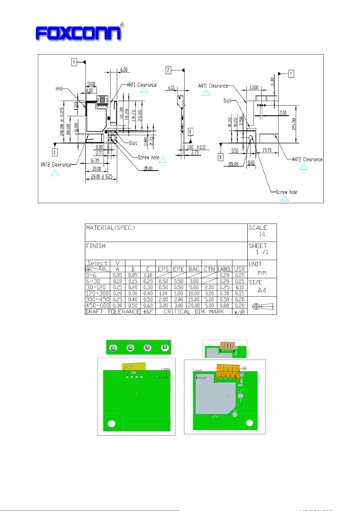
Ⅰ.For J26H006.C01: Typical module dimension (W x L) is 28mmx28mm.
5
Page 6
COMPANY CONFIDENTIAL
Unit: mm
The tolerance for each mechanical dimension
1
Note
: The max shift degree of WTB connector is 2.3degree.
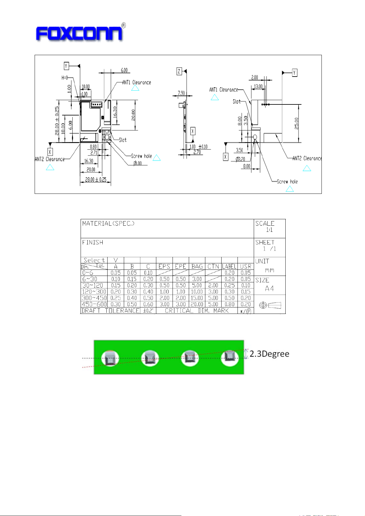
Ⅱ. For J26H006.B01: Typical module dimension (W x L) is 28mmx28mm.
6
Page 7
COMPANY CONFIDENTIAL
The tolerance for each mechanical dimension
Unit: mm
2
Note
: The max shift degree of BTB connector is 2.3degree.
2.2 USB Connector
Ⅰ.For J26H006.C01:WTB Connector
¾ 4pin, 2.0mm pitch, Right angle type
¾ Part number: HFK2040-G1C3K-8F
¾ Vendor: Foxconn FIT
¾ High temperature plastic PA9T which meet SMT reflow profile(PIP)
7
Page 8
COMPANY CONFIDENTIAL
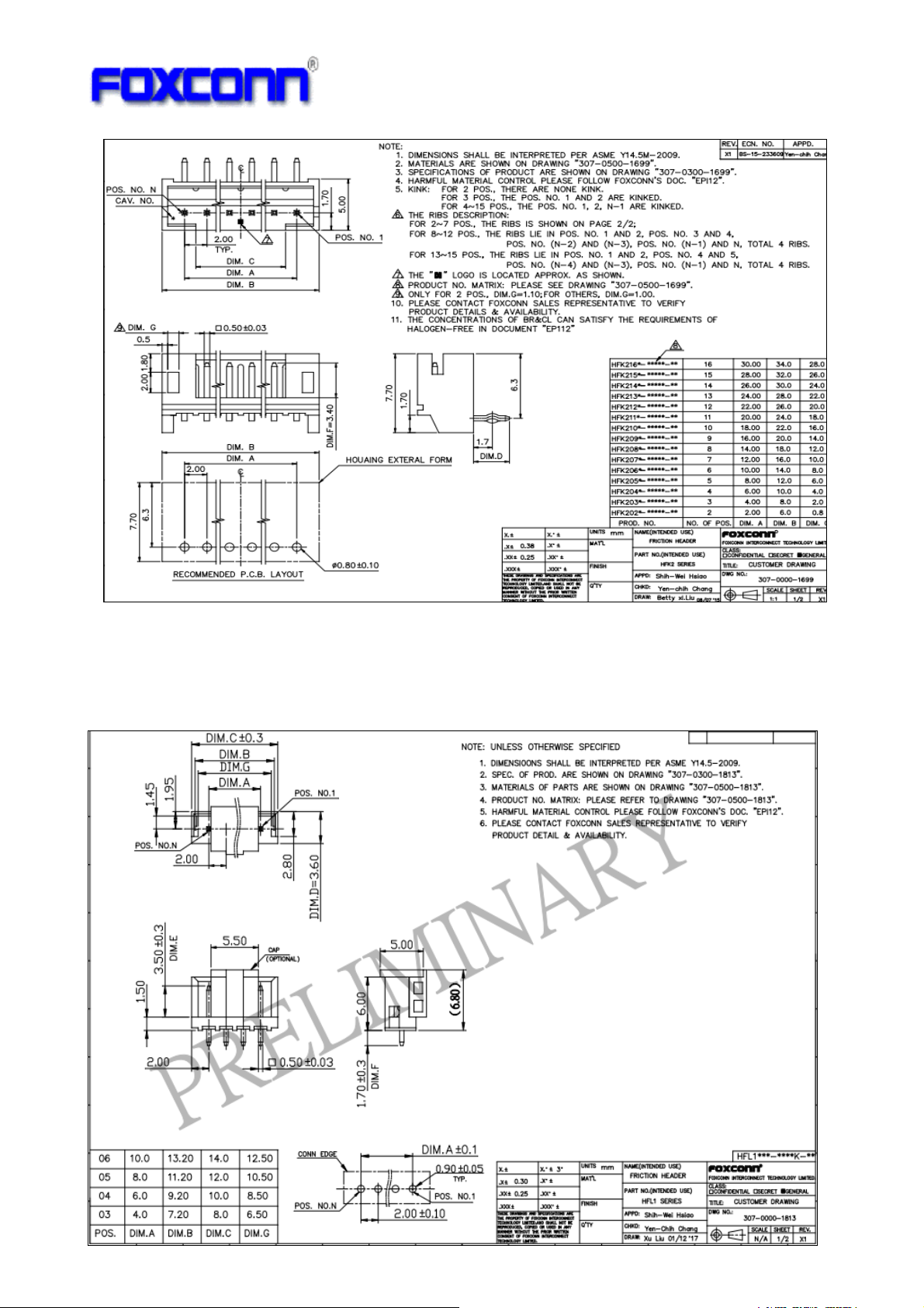
Ⅱ. For J26H006.B01: BTB Connector
¾ 4pin, 2.0mm pitch, Vertical type
¾ Part number: HFL1040-G1C3K-9F
¾ Vendor: Foxconn FIT
¾ High temperature plastic PA9T which meet SMT reflow profile(PIP)
8
Page 9
COMPANY CONFIDENTIAL
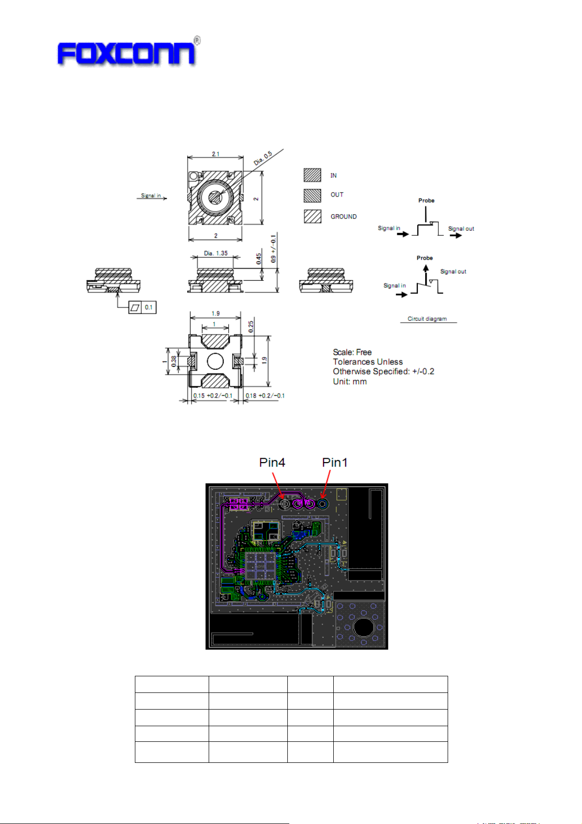
2.3 RF Switch Connector
¾ Part number: MM8030-2610RJ3
¾ Vendor: Murata
3.USB Connector Pin-out
Pin Number Pin Name I/O Description
1 VDD33 I DC 3.3V source input
2 USB_DN I/O USB D- Signal
3 USB_DP I/O USB D+ Signal
4 GND -- Ground
9
Page 10
COMPANY CONFIDENTIAL
5. Electrical Specification
5.1 Recommended Operating Condition
Symbol Condition Min. Typ. Max Unit
3.3v(VDD33) Respect to GND 3.0 3.3 3.6 V
Max Ripple on Supplied Voltage 3.3V @full loading 95 330 mVpp
DC current @3.3V at full loading
(WiFi @TX and BT @ TX)
USB Suspend current -- 3.6 6 mA
Operating Temperature 0 +25 +70
Storage Temperature -25 25 +85
Operating Humidity 30~50% 90% RH
ESD HBM(contact) Standard:MIL-STD-883H +/-1.5 KV
ESD (indirect) Standard:EN61000-4-2 +/-4 KV
Function operation is not guaranteed outside of this limit, and operation outside of this limit for extended
period can adversely affect long-term reliability of the device.
- 257 500 mA
℃
℃
5.2 RF Characteristics
All typical performance specification are measured at RF connector port operating in +25℃@3.3V
3
: The target power table is just defined for board level.
Note
4
: Power is compliance with EVM IEEE spec based-on the parameter “disable full packet”
Note
Standard IEEE802.11b/g/n
Data Rate
Bandwidth 20MHz for 2.4GHz,
Modulation Techniques
Operating Frequency 2.412GHz~2.462GHz,
Media Access Control CSMA/CA with ACK
WiFi
Transmit Output Power
Frequency error +/-10ppm
Receiver Sensitivity
Radio Modulation FHSS
Operating Frequency 2.402GHz ~ 2.480GHz
Channel Numbers 79 channels with 1MHz BW
BDR Transmitter Output
Power
BDR Power Control 2dB≤Power Control Step≤8dB
BDR Initial Carrier Freq.
Tolerance
802.11b: 11, 5.5, 2, 1 Mbps;
802.11g: 54, 48, 36, 24, 18, 12, 9, 6 Mbps
802.11n:
HT20 mode: MCS0~MCS7,up to 72.2Mbp
802.11b: CCK, DQPSK, DBPSK
802.11g: 64QAM,16QAM, QPSK, BPSK
802.11n: 64QAM,16QAM, QPSK, BPSK
11b CCK_11Mbps:
11g 54Mbps: 25d
11n HT20_MCS7: 25dBm+/-1.5dB
11b 11Mbps: -83dBm@PER<=8%
11g 54Mbps: -70dBm@PER<=10%
11n HT20 MCS7: -67dBm@PER<=10%
0~+14dBm
≤ ± 75 kHz
23dBm+/-1.5dB
Bm+/-1.5dB
10
Page 11
COMPANY CONFIDENTIAL
BDR Carrier Frequency
Drift
BDR Modulation
Characteristics
BDR Maximum Receiver
Signal
BDR Sensitivity -85dBm @ BER <= 0.1% at 1Mbps
BT
EDR Relative Power P[GFSK]-4dB<P[DPSK]< P[GFSK]+1dB
EDR Stability and Mod
Accuracy
BDR Frequency Range FL>2.4GHz,FH<2.4835GHz
EDR Sensitivity -80dBm@BER <= 0.01% at 2Mbps
BDR TX Output Spectrum
-20dB Bandwidth
LE Output Power 0~+14dBm
LE Modulation
Characteristics
LE Carrier frequency
offset and drift
LE Receiver Sensitivity -90dBm@PER <= 30.8%,GFSK,1Mbps
Drift Rate/50us <±20kHz
DH1: +/- 25kHz,DH3: +/- 40kHz,DH5: +/- 40kHz
140kHz ≤ ∆f1avg ≤175kHz
∆f2max ≥115kHz
∆f2avg/∆f1avg ≥0.8
-20dBm@ BER <= 0.1% at 1Mbps
-75 kHz <ωi < 75 kHz
-10kHz<ω0 <10kHz
RMS DEVM<=0.13 for all 8DPSK @3Mbps
Peak DEVM<=0.25 for all 8DPSK @3Mbps
99% DEVM<=0.2 for 99% 8DPSK @3Mbps
-80dBm@BER <= 0.01% at 3Mbps
≤1MHz
225kHz ≤ ∆f1avg ≤275kHz;
∆f2max ≥185kHz for at least 99.9% test packets;
∆f2avg/∆f1avg ≥0.8
Carrier frequency offset: ±150kHz
Carrier Drift: ≤50kHz
Drift rate: ≤20kHz/50us
5.3 Current consumption
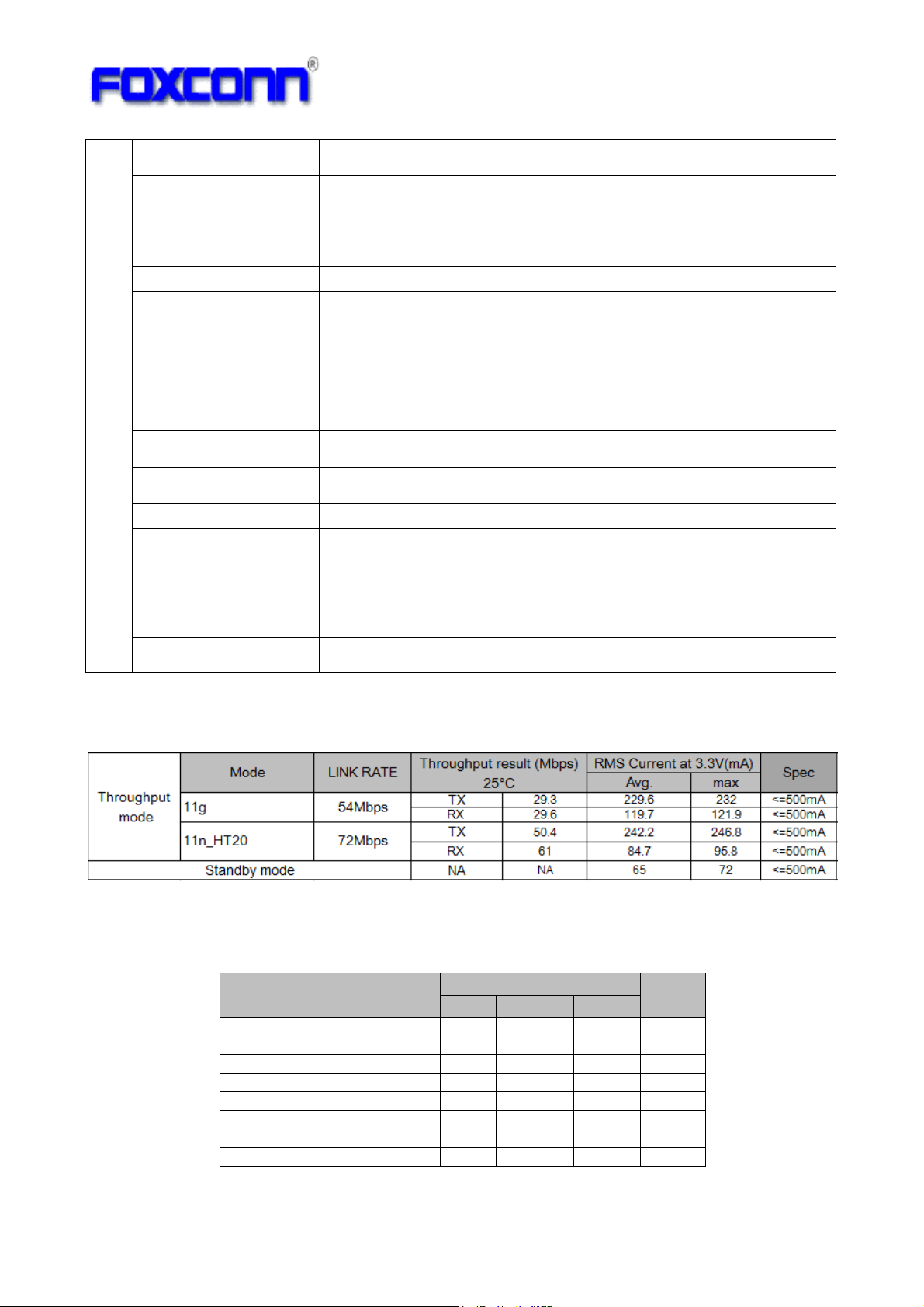
5.3.1 WiFi current consumption
Remark: Base-on Win7 OS to do WiFi only throughput tests. The Standby mode means “module connect to
AP only, and don’t transfer the data.”
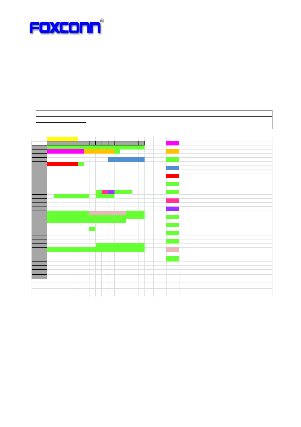
5.3.2 Bluetooth current consumption
Test Condition
Idle mode( power on only) 63.7 mA
BT BDR 1DH5 TX@6dBm 115 mA
BT BDR 1DH5 Rx 87 mA
BT EDR 2DH5 TX@6dBm 116 mA
BT EDR 2DH5 Rx 87 mA
BLE TX@6dBm 78 mA
BLE Rx 87 mA
Standby mode* 69 mA
Avg. Current at 3.3V
Min Typ. Max
Unit
Remark: The result is base-on Win7 driver.
The Idle mode means “ module power on only, don’t open any testing tool”
The standby mode means “module connect to BT device only, and don’t transfer the data”
11
Page 12
COMPANY CONFIDENTIAL
C
5.4 eFuse Content
5.4.1 WiFi eFuse
Revision Note
EEPROM Version Chang Lists Owner Date Remark
address Value for WiFi Efuse address 0xC4, change
0xC4 0x01
value from 0x00 to 0x01
address 0 1 2 3 4 5 6 7 8 9 A B C D E F Path A cck TX calibration power index
eFuse for WiFi eFuse address
0 29 81007C01880700 A004 EC3512C0A2D8
1 16 1413121212191817 161602FFFFFFFF Path A 11n HT40 mcs7 TX calibratio n
2 FF FFFFFF FFFFFFFFFF FFFFFFFFFFFFFF
3 FF FFFFFFFFFFFFFFFF FF141414131212 0x1B Path A pow er diff in dex (offse t) fixed value
4 17 1717161502FFFFFF FF FFFFFFFFFFFF
5 FF FF FF FF FF FF FF FF FF FF FF FF FF FF FF FF Path B cck TX power calibration index
6 FF FFFFFF FFFFFFFFFF FFFFFFFFFFFFFF
7 FF FF FF FF FF FF FF FF FF FF FF FF FF FF FF FF Path B 11n HT40 mcs7 TX calibration power index
8 FF FFFFFF FFFFFFFFFF FFFFFFFFFFFFFF
9 FF FFFFFF FFFFFFFFFF FFFFFFFFFFFFFF 0x45 Path B power diff index(offset) fixed value
A FF FFFFFFFFFFFFFFFF FF FFFFFFFFFFFF
B FFFFFFFFFFFFFFFF20 1F1A000000FFFF 0xB8 channel plan:0x20 fixed value
C FF292050010000FF00 FF11FFFFFFFFFF
D FF FFFFFFFFFFFFFFFF FF FFFFFFFFFFFF 0xB9 Crystal calibration data
E FFFFFFFFFFFFFFFFFF FF FFFFFFFFFFFF
F FFFFFFFFFFFFFFFFFF FF FFFFFFFFFFFF 0xBA Thermal meter
10 DA 0B 23 D7 E7 46 07 D8 0F 99 16 57 F3 09 03 52
11 65 61 6C 74 65 6B 16 03 38 30 32 2E 31 31 6E 20 0xC3 Antann a settin g fixed value
12 57 4 C 41 4E 20 4 1 64 61 70 74 65 72 00 FF FF FF
13 FF FF FF FF FF FF FF FF FF FF FF FF FF FF FF FF 0xC4 EEPROM version: 0x01 fixed value
14 FF FF FF FF FF FF FF 0F FF F F FF FF FF FF FF FF
15 FF FF FF FF FF FF FF FF FF FF FF FF FF FF FF FF 0x100~0x101 VID:0x0BDA fixed value
16 FF FF FF FF FF FF FF FF FF FF FF FF FF FF FF FF
17 FF FF FF FF FF FF FF FF FF FF FF FF FF FF FF FF 0x102~0x103 PID:0xD723 fixed value
18 FF FF FF FF FF FF FF FF 6 B 41 22 D D 53 59 86 D1
19 70 8F 00 00 10 16 40 00 FC 8C 00 11 9B 00 00 0A 0x107~0x10
1A FF FF FF FF FF FF FF FF FF FF FF FF FF FF FF FF
1B FF FF FF FF FF FF FF FF FF FF FF FF FF FF FF FF 0x00~0x0F
1C FF FF FF FF FF FF FF FF FF FF FF FF FF FF FF FF 0xBB~0xBD
1D FF FF FF FF FF FF FF FF FF FF FF FF FF FF FF FF 0xC1~0xC2
1E FF FF FF FF FF FF FF FF FF FF FF FF FF FF FF FF 0xC4~0xC6
1F FF FF FF FF FF FF FF FF FF FF FF FF FF FF FF FF 0xC8~0xCa
Note:
USB Vendor ID (VID): 0x0BDA
USB Product ID (PID): 0xD723
Fly. Huang 2017/08/11 PVT
WiFi MAC: D80F991657F3 consistency
other config fixed vuale
0x104~0x12C
0x147
0x188~0x19F
12
Page 13

5.4.2 BT eFuse
COMPANY CONFIDENTIAL
13
Page 14
COMPANY CONFIDENTIAL
n
eFuse for BT
address 0 1 2 3 4 5 6 7 8 9 A B C D E F Efuse address description Value
0 FFFFFFFF FF FFFF FF FFFF FF FF FFFFFFFF
1 FF FF FF FF FF FF FF FF FF FF FF FF FF FF FF FF 0x44~0x49 BT MAC address F8DA0C5D2618 No t fixed valu e
2 FFFFFFFF FF FFFF FF FFFF FF FF FFFFFFFF
3 FFFFFFFF FF FFFF FF FFFF FF FF FFFFFFFF 0xDA~0xDB default value from IC 10,D8 Fixed value
4 FFFFFFFF 18 265D 0CDAF8 FF FF FFFFFFFF 0x1F4~0x1F7 default value from IC 94,80,06,00 Fixed value
5 FFFFFFFF FF FFFF FF FFFF FF FF FFFFFFFF
6 FF FF FF FF FF FF FF FF FF FF FF FF FF FF FF FF 0x15B~0x15E BT TX power calibration in dex Not fixe d va lue
7 FF FF FF FF FF FF FF FF FF FF FF FF FF FF FF FF 0x15B 1M power index 1E
8 FF FF FF FF FF FF FF FF FF FF FF FF FF FF FF FF 0x15C 2M power index 1F
9 FF FF FF FF FF FF FF FF FF FF FF FF FF FF FF FF 0x15D 3M power index 1F
A FF FF FF FF FF FF FF FF FF FF FF FF FF FF FF FF 0x15E LE power index 1F
B FFFFFFFFFF FFFF FF FF FF FF FF FFFFFFFF
C FFFFFFFFFF FFFF FF FF FF FF FF FFFFFFFF 0x15F BT Tx gain step 01 Fixed value
D FFFFFFFFFF FFFF FF FF FF 10 D8 FFFFFFFF
E FF FF FF FF FF FF FF FF FF FF FF FF FF FF FF FF 0x188~0x189 BT Thermal value index 00,1F Not fixed value
F FFFFFFFFFFFFFF FF FFFF FFFF FFFFFFFF
10 FF FF FF FF FF FF FF FF FF FF FF FF FF FF FF FF 0x1CE~0x1CF BT Antenna info F7,3E Fixed value
11 FF FF FF FF FF FF FF FF FF FF FF FF FF FF FF FF
12 FF FF FF FF FF FF FF FF FF FF FF FF FF FF FF FF 0x1E4~0x1E5 BT Modem tx gain compensatio
13 FF FF FF FF FF FF FF FF FF FF FF FF FF FF FF FF
14 FF FF FF FF FF FF FF FF FF FF FF FF FF FF FF FF 0x1E6 BT Xtal cap 1E Not fixed value
15 FF FF FF FF FF FF FF FF FF FF 27 1E 1F 1F 1F 01
16 FF FF FF FF FF FF FF FF FF FF FF FF FF FF FF FF
17 FF FF FF FF FF FF FF FF FF FF FF FF FF FF FF FF
18 FF FF FF FF FF FF FF FF 00 1 F FF FF FF FF FF FF
19 FF FF FF FF FF FF FF FF FF FF FF FF FF FF FF FF
1A FF FF FF FF FF FF FF FF FF FF FF FF FF FF FF FF
1B FF FF FF FF FF FF FF FF FF FF FF FF FF FF FF FF
1C FF FF FF FF FF FF FF FF FF FF FF FF FF FF F7 3 E
1D FF FF FF FF FF FF FF FF FF FF FF FF FF FF FF FF
1E FF FF FF FF 33 33 1 E FF FF FF FF FF FF FF FF FF
1F FF FF FF FF 94 80 06 00 FF FF FF FF FF FF FF FF
20 FF FF FF FF FF FF FF FF FF FF FF FF FF FF FF FF
21 FF FF FF FF FF FF FF FF FF FF FF FF FF FF FF FF
22 FF FF FF FF FF FF FF FF FF FF FF FF FF FF FF FF
23 FF FF FF FF FF FF FF FF FF FF FF FF FF FF FF FF
24 FF FF FF FF FF FF FF FF FF FF FF FF FF FF FF FF
25 FF FF FF FF FF FF FF FF FF FF FF FF FF FF FF FF
26 FF FF FF FF FF FF FF FF FF FF FF FF FF FF FF FF
27 FF FF FF FF FF FF FF FF FF FF FF FF FF FF FF FF
28 FF FF FF FF FF FF FF FF FF FF FF FF FF FF FF FF
29 FF FF FF FF FF FF FF FF FF FF FF FF FF FF FF FF
2A FF FF FF FF FF FF FF FF FF FF FF FF FF FF FF FF
2B FF FF FF FF FF FF FF FF FF FF FF FF FF FF FF FF
2C FF FF FF FF FF FF FF FF FF FF FF FF FF FF FF FF
2D FF FF FF FF FF FF FF FF FF FF FF FF FF FF FF FF
2E FF FF FF FF FF FF FF FF FF FF FF FF FF FF FF FF
2F FF FF FF FF FF FF FF FF FF FF FF FF FF FF FF FF
30 FF FF FF FF FF FF FF FF FF FF FF FF FF FF FF FF
31 FF FF FF FF FF FF FF FF FF FF FF FF FF FF FF FF
32 FF FF FF FF FF FF FF FF FF FF FF FF FF FF FF FF
33 FF FF FF FF FF FF FF FF FF FF FF FF FF FF FF FF
31 FF FF FF FF FF FF FF FF FF FF FF FF FF FF FF FF
35 FF FF FF FF FF FF FF FF FF FF FF FF FF FF FF FF
36 FF FF FF FF FF FF FF FF FF FF FF FF FF FF FF FF
37 FF FF FF FF FF FF FF FF FF FF FF FF FF FF FF FF
38 FF FF FF FF FF FF FF FF FF FF FF FF FF FF FF FF
39 FF FF FF FF FF FF FF FF FF FF FF FF FF FF FF FF
40 FF FF FF FF FF FF FF FF FF FF FF FF FF FF FF FF
41 FF FF FF FF FF FF FF FF FF FF FF FF FF FF FF FF
42 FF FF FF FF FF FF FF FF FF FF FF FF FF FF FF FF
43 FF FF FF FF FF FF FF FF FF FF FF FF FF FF FF FF
44 FF FF FF FF FF FF FF FF FF FF FF FF FF FF FF FF
45 FF FF FF FF FF FF FF FF FF FF FF FF FF FF FF FF
33,3 3 No t fixed value
5.5 Power On/Off Sequence
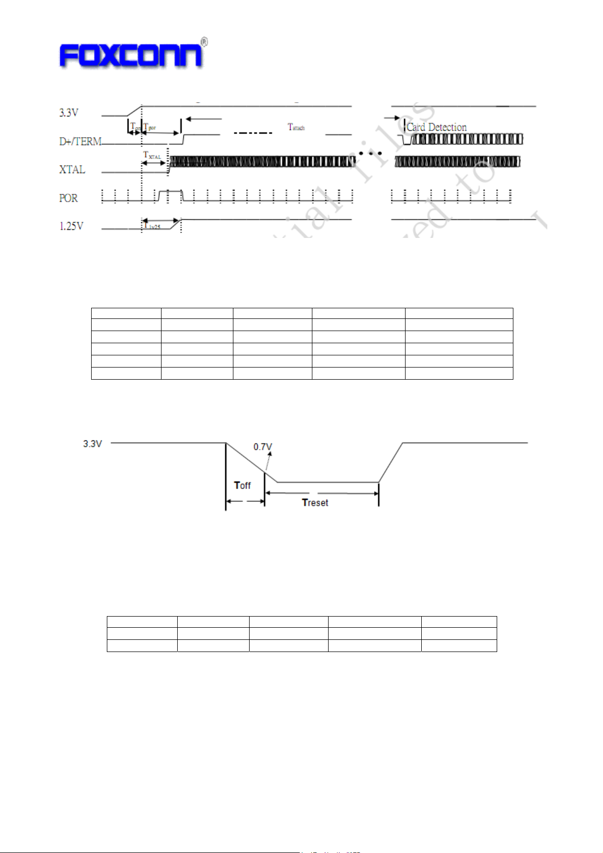
5.5.1 Power On Sequence
14
Page 15
COMPANY CONFIDENTIAL
Ton: The main power ramp up duration
Tpor: The power on reset releases and power management unit executes power on tasks
Tattach: USB attach state
Item Min. Typ. Max Uint
Ton 0.2 1.5 5 ms
Tpor -- 2 10 ms
Txtal -- 1.5 8 ms
Tattach 100 250 -- ms
T1v25 -- 2 5 ms
5.5.2 Power Off Sequence
Toff: The main power ramp down duration (from 3.3V fall to 0.7V).
VDD33(3.3V) is coming from system, different DC power supply’s load cap value may cause the
different discharge time.
Treset:
To assert Chip reset, keep the VDD33 under 0.7V for 100ms
Item Min. Typ. Max Unit
Toff -- 16 1000 ms
Treset 100 -- -- ms
15
Page 16
5.6 Floating pin status
COMPANY CONFIDENTIAL
5.7 Antenna Specification
16
Page 17
COMPANY CONFIDENTIAL
17
Page 18
COMPANY CONFIDENTIAL
5.8 Operating System Support
Support the Win7, Win8.1, Win10, Linux operating system on normal driver
18
Page 19
COMPANY CONFIDENTIAL
6. Label Information
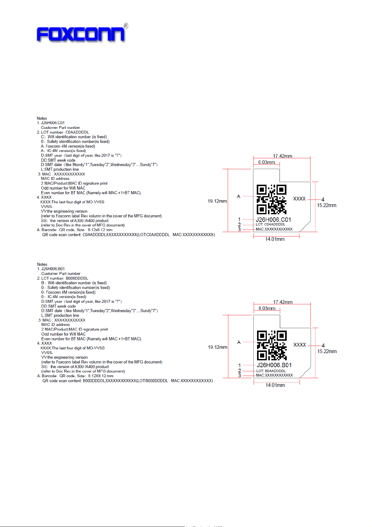
6.1 MAC-ID Label Laser Marking
All content is engraved by laser into shielding cover.
Ⅰ.For J26H006.C01
Ⅱ. For J26H006.B01
19
Page 20
COMPANY CONFIDENTIAL
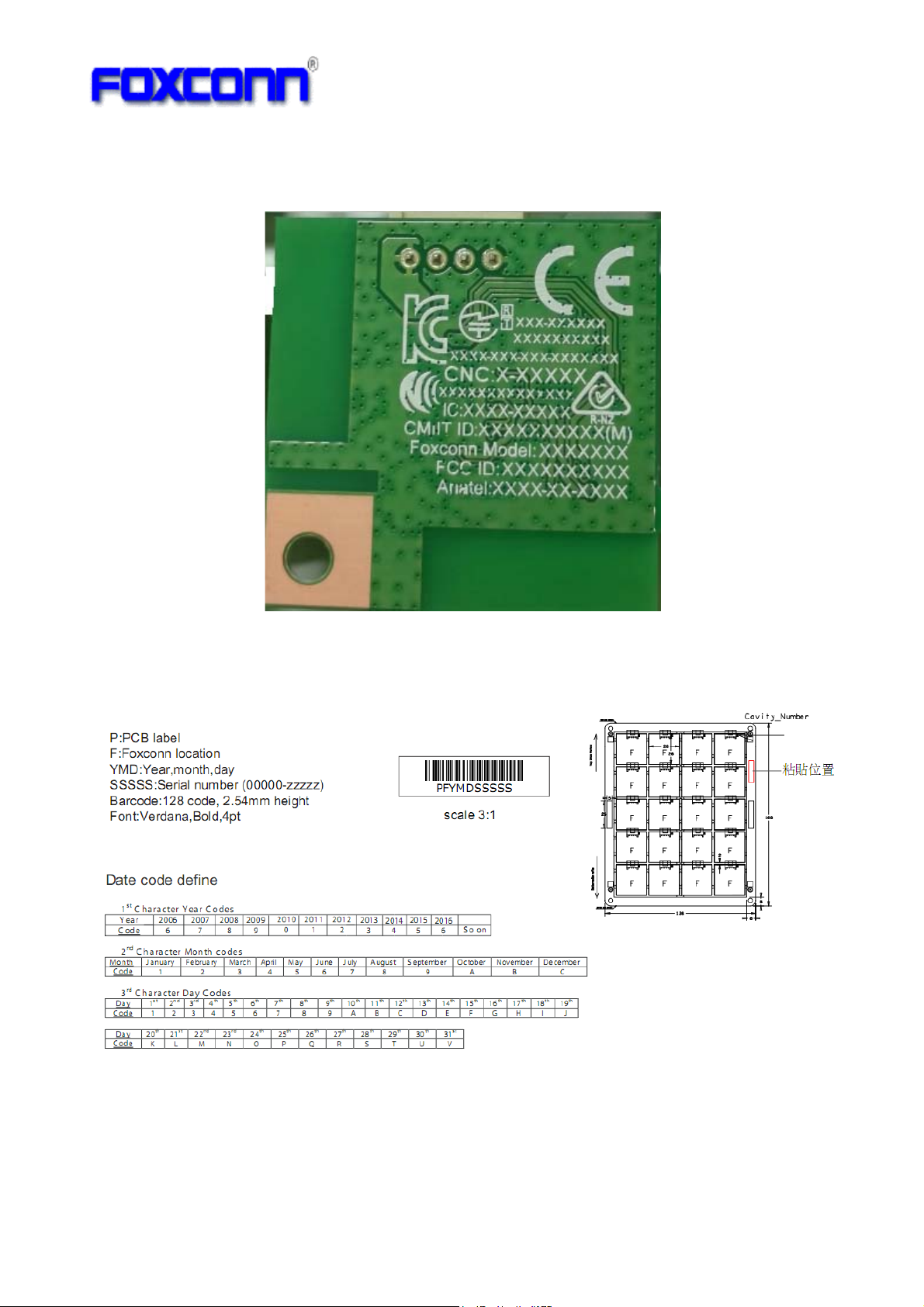
6.2 Regulatory Label
Regulatory label was printed on PCB Bottom side for PVT, it will be updated after get the
official regulatory ID.
6.3 Panel Label
20
Page 21
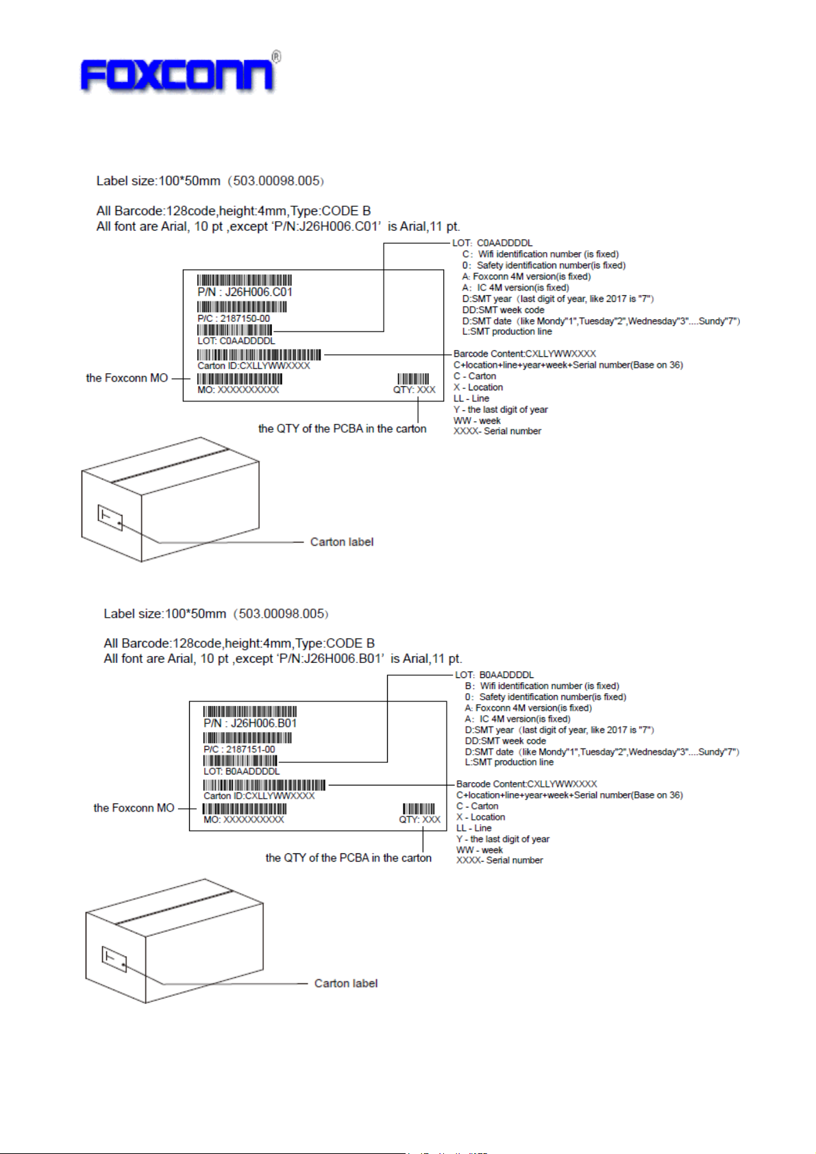
6.4 Carton Label
Ⅰ.For J26H006.C01
COMPANY CONFIDENTIAL
Ⅱ. For J26H006.B01
6.5 Pallet Label
Ⅰ.For J26H006.C01
21
Page 22

COMPANY CONFIDENTIAL
Ⅱ.For J26H006.B01
22
Page 23
COMPANY CONFIDENTIAL
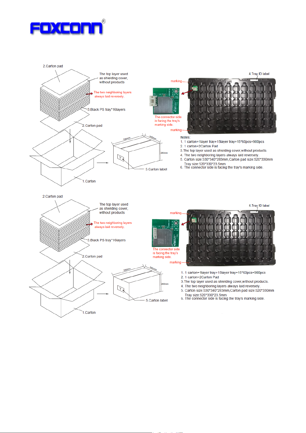
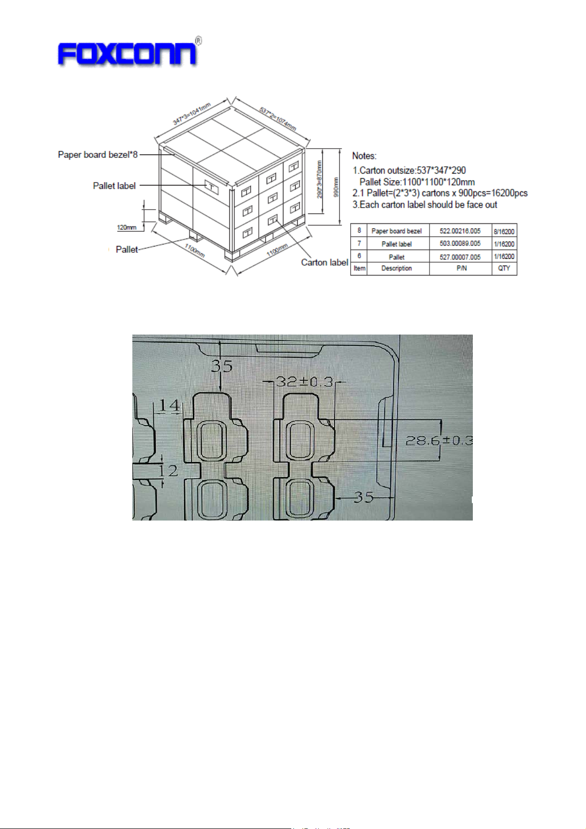
7. Packing Information
I:For J26H006.C01
II:For J26H006.B01
23
Page 24
COMPANY CONFIDENTIAL
The detailed dimension of the tray
z The hollow length and side value
z The distance between module and module, and between module and outline of tray
24
Page 25

COMPANY CONFIDENTIAL
7.1 Module Scan Guide
1. Taking the module in declining way about 45° to prevent the shielding reflecting
the lightness;
2. Taking the scanner and turning right in 45° angle;
Note: The distance between scanner and module is about 5-8cm
25
Page 26

COMPANY CONFIDENTIAL
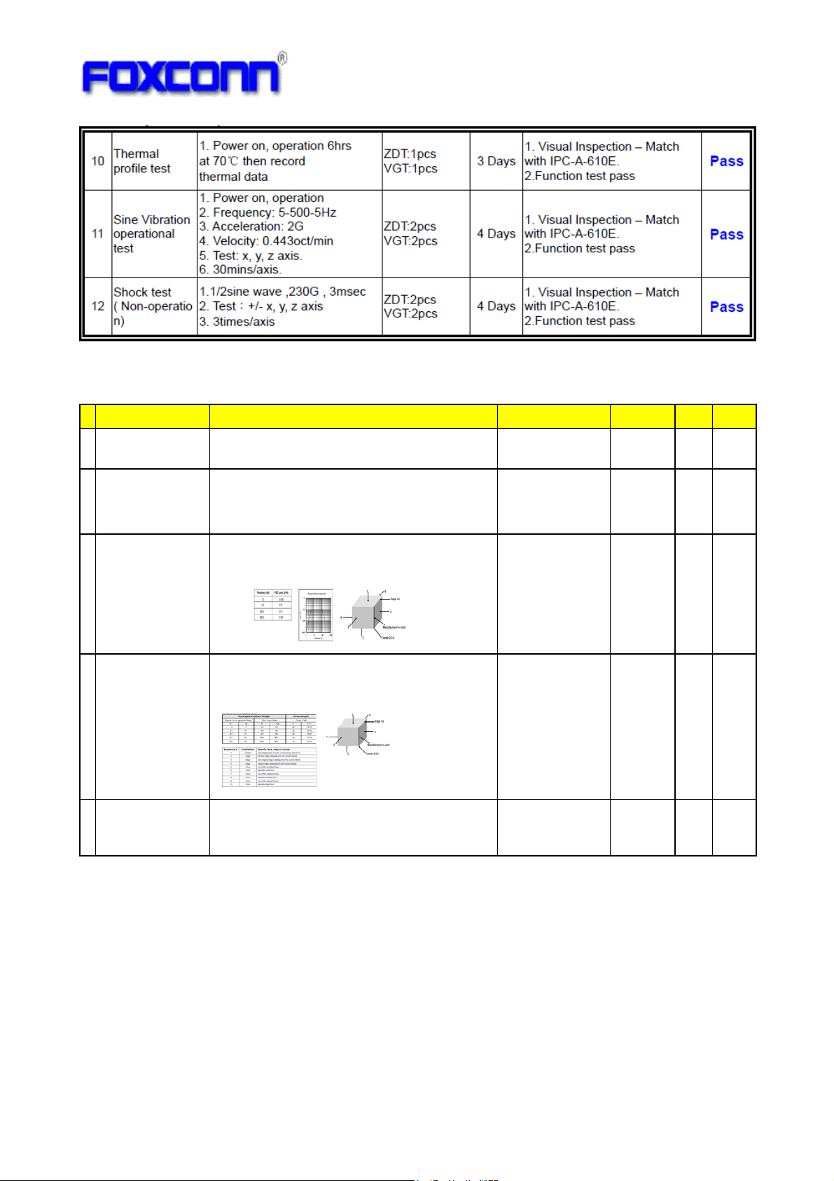
8. Reliability
8.1 Hardware Reliability Test
26
Page 27
COMPANY CONFIDENTIAL
8.2 Package Reliability Test (TBD)
The product shall pass below package reliability test plan.
No Test Items Description Test Criteria Reference Qty' Result
1 Atmosph eric Conditioning
2 Static Comp ression T est
3 Random Vibration Test
Test Temlpearture: 38
Test humidity: 85%R.H.
Dwell time: 72hours
Units are packaged
Compression load=Wt x (S - 1) x F
Wt:Total weitht of th e packaged-p rocuct
S:Total number of packaged-products in a stack
1:Represents the bottom container in a Stack
Compression Test duration:1hour
The following breakpoints shall be programmed into the vibration
controller to produce the acceleration versus frequency profile (spectrum)
below with an overall Grm s level of 1.15.
Face 3: 30mins, Face1: 10mins, Face 2 or 4: 10mins, Face 5 or 6: 10mins
℃
No obvious visible damage
on boxes after temperature
and humidity test.
No obvious visible damage
on boxes after static
compression test.
No obvious visible damage
on boxes after random
vibration test.
ISTA-2A 1carton TBD
ISTA-2A 1carton TBD
ISTA-2A 1carton TBD
The test drop height var ies with the weig ht of the pac kaged-product.
Find the weight of the packaged-product in the following chart to
determine a drop height or an equivalent impact velocity to
be used for a substituted drop:
No obvious visible damage
4Package drop test
5 Fix displacement Test
Displacement:25mm
Duration:14200times
on boxes after packaged
drop test.
No obvious visible damage
on boxes after fixed
displacement test.
ISTA-2A 1carton TBD
ISTA-2A 1carton TBD
9. Quality
The product quality must be followed-up by Foxconn factory quality control system.
In accordance with SEIKO EPSON Group's requirements specified by the latest “Electronic
Component Quality Requirements Standard" and "WiFi+BT Combo Module Quality
Requirements Specification Rev.B" , the product shall be managed Quality control.
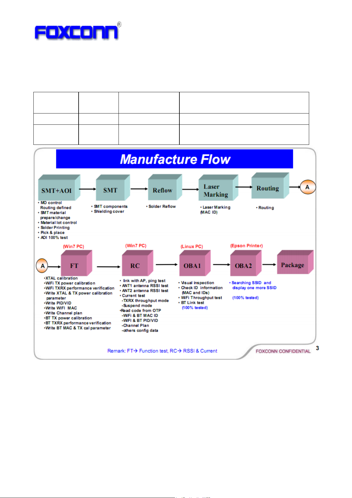
9.1 QC Flow Chart
27
Page 28
COMPANY CONFIDENTIAL
9.2 Visual Inspection Standard
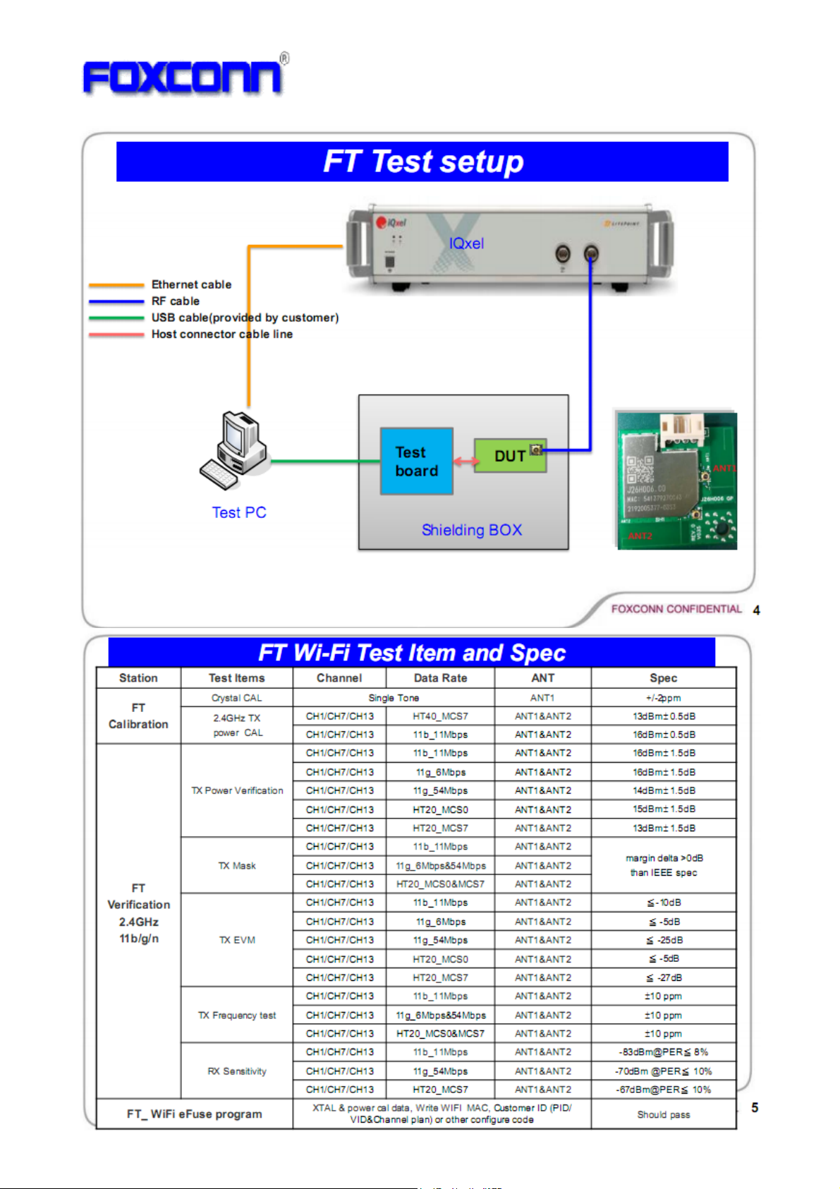
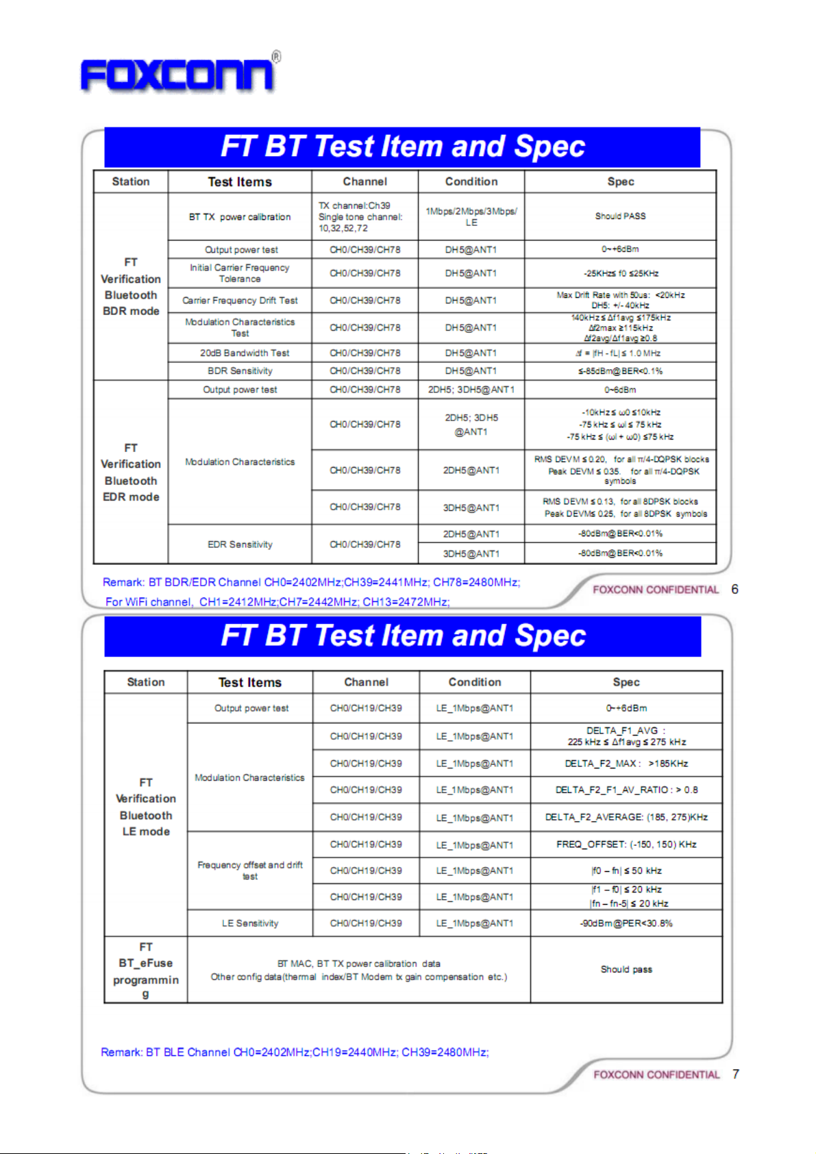
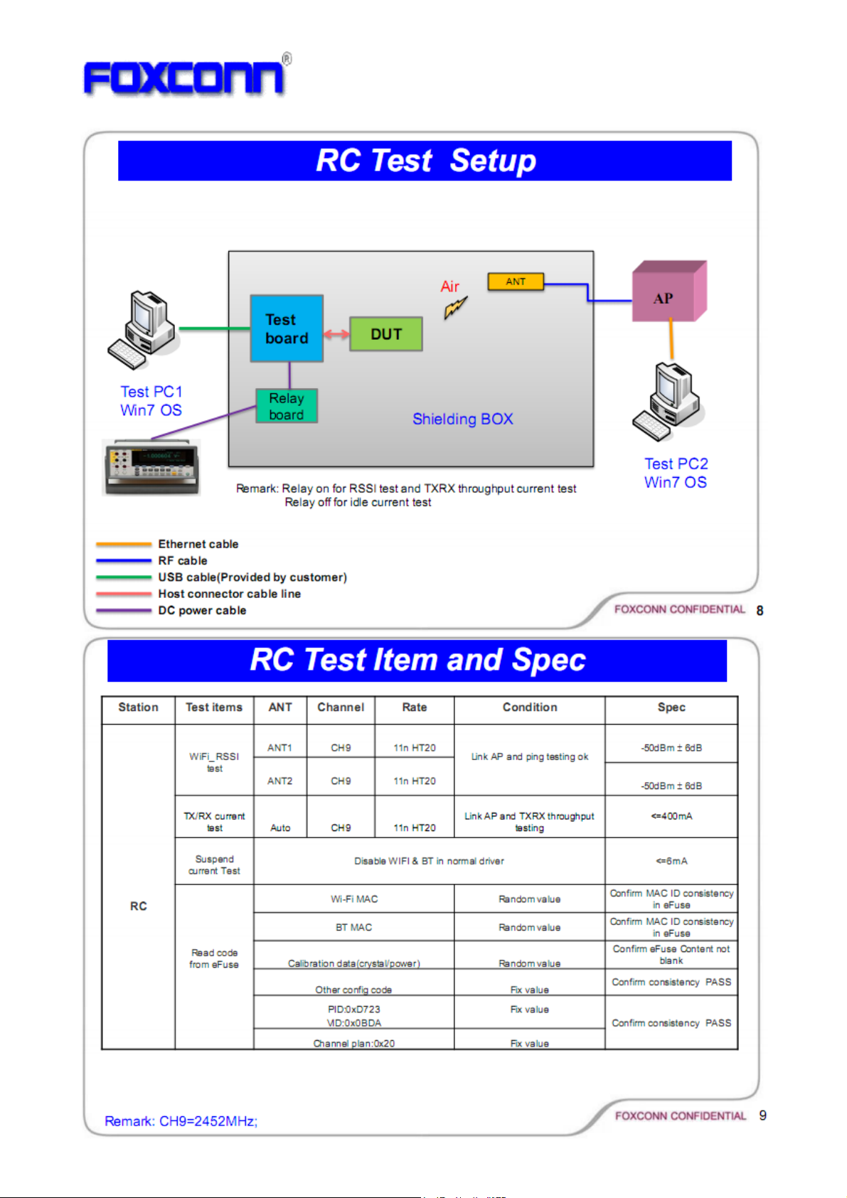
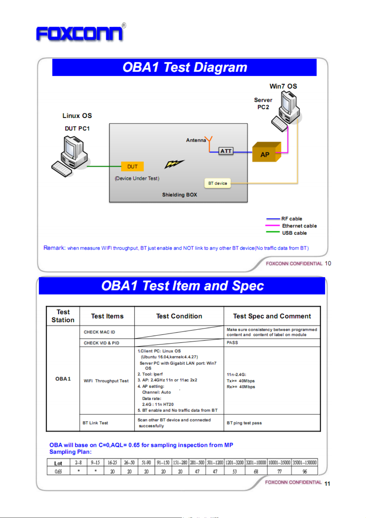
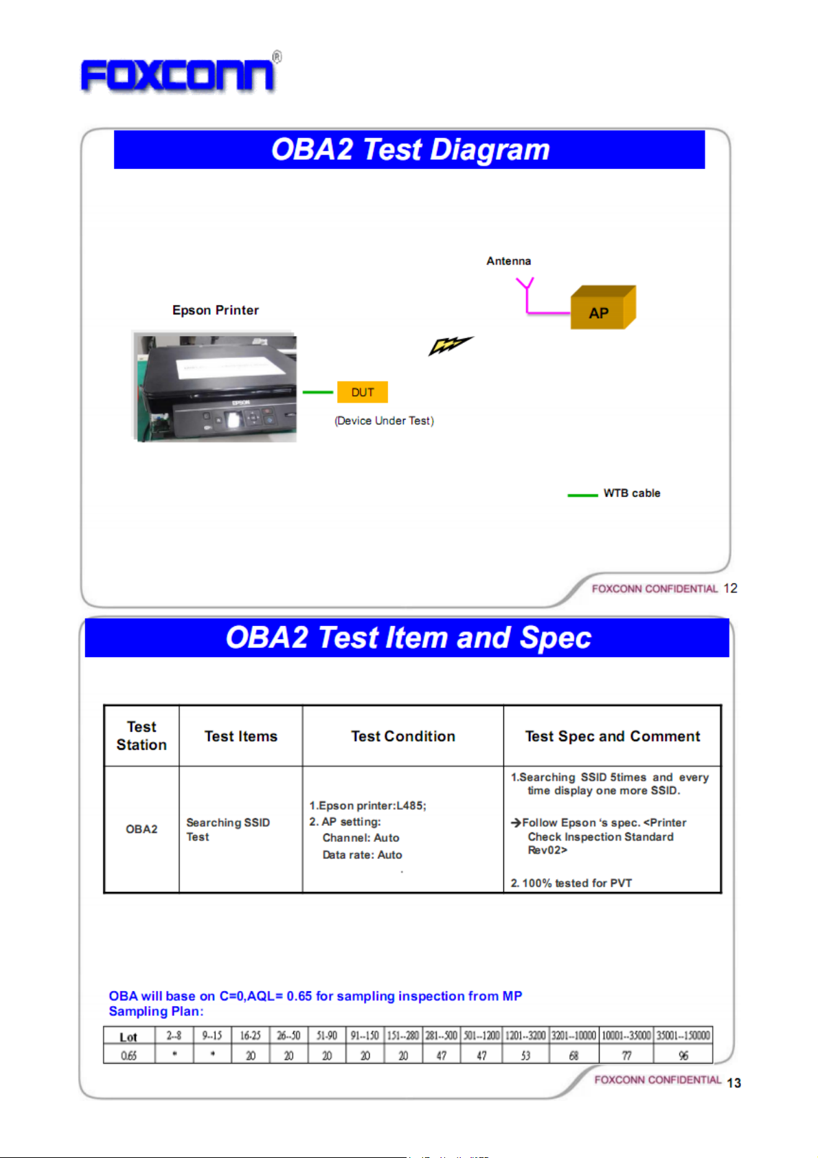
9.3 PVT Mfg. Test Plan
Date
2017/08/3
Version
V1.7 Fly Huang
Author
Change Description
Initial released
28
Page 29
COMPANY CONFIDENTIAL
29
Page 30
COMPANY CONFIDENTIAL
30
Page 31
COMPANY CONFIDENTIAL
31
Page 32
COMPANY CONFIDENTIAL
32
Page 33
COMPANY CONFIDENTIAL
33
Page 34

Federal Communication Commission Interference Statement
This device complies with Part 15 of the FCC Rules. Operation is subject to the
following two conditions: (1) This device may not cause harmful interference, and (2)
this device must accept any interference received, including interference that may
cause undesired operation.
This equipment has been tested and found to comply with the limits for a Class B
digital device, pursuant to Part 15 of the FCC Rules. These limits are designed to
provide reasonable protection against harmful interference in a residential installation.
This equipment generates, uses and can radiate radio frequency energy and, if not
installed and used in accordance with the instructions, may cause harmful
interference to radio communications. However, there is no guarantee that
interference will not occur in a particular installation. If this equipment does cause
harmful interference to radio or television reception, which can be determined by
turning the equipment off and on, the user is encouraged to try to correct the
interference by one of the following measures:
- Reorient or relocate the receiving antenna.
- Increase the separation between the equipment and receiver.
- Connect the equipment into an outlet on a circuit different from that
to which the receiver is connected.
- Consult the dealer or an experienced radio/TV technician for help.
FCC Caution: Any changes or modifications not expressly approved by the
party responsible for compliance could void the user's authority to operate this
equipment.
This transmitter must not be co-located or operating in conjunction with any
other antenna or transmitter.
Page 35

Radiation Exposure Statement:
This equipment complies with FCC radiation exposure limits set forth for an
uncontrolled environment. This equipment should be installed and operated
with minimum distance 20cm between the radiator & your body.
This device is intended only for OEM integrators under the following
conditions:
1) The antenna must be installed such that 20 cm is maintained between the
antenna and users, and
2) The transmitter module may not be co-located with any other transmitter or
antenna.
As long as 2 conditions above are met, further transmitter
required. However, the OEM integrator is still responsible for testing their
end-product for any additional compliance requirements required with this
module installed
IMPORTANT NOTE: In the event that these conditions can not be met
example certain laptop configurations or co-location with another transmitter),
then the FCC authorization is no longer considered valid and the FCC ID can
not be used on the final product. In these circumstances, the OEM integrator
will be responsible for re-evaluating the end product (including the transmitter)
and obtaining a separate FCC authorization.
End Product Labeling
This transmitter module is authorized only for use in device where the antenna
may be installed such that 20 cm may be maintained between the antenna
and users. The final end product must be labeled in a visible area with the
following: “Contains FCC ID: BKMFBJ26H006”. The grantee's FCC ID can be
test will not be
(for
used only when all FCC compliance requirements are met.
Manual Information To the End User
The OEM integrator has to be aware not to provide information to the end user
regarding how to install or remove this RF module in the user’s manual of the
end product which integrates this module.
The end user manual shall include all required regulatory information/warning
as show in this manual.
Industry Canada statement:
Page 36

This device complies with ISED’s licence-exempt RSSs. Operation is subject to the
following two conditions: (1) This device may not cause harmful interference, and (2)
this device must accept any interference received, including interference that may
cause undesired operation.
Le présent appareil est conforme aux CNR d’ ISED applicables aux appareils radio
exempts de licence. L’exploitation est autorisée aux deux conditions suivantes : (1) le
dispositif ne doit pas produire de brouillage préjudiciable, et (2) ce dispositif doit
accepter tout brouillage reçu, y compris un brouillage susceptible de provoquer un
fonctionnement indésirable.
Radiation Exposure Statement:
This equipment complies with ISED radiation exposure limits set forth for an
uncontrolled environment. This equipment should be installed and operated with
minimum distance 20cm between the radiator & your body.
Déclaration d'exposition aux radiations:
Cet équipement est conforme aux limites d'exposition aux rayonnements ISED
établies pour un environnement non contrôlé. Cet équipement doit être installé et
utilisé avec un minimum de 20 cm de distance entre la source de rayonnement et
votre corps.
This device is intended only for OEM integrators under the following conditions:
(For module device use)
1) The antenna must be installed such that 20 cm is maintained between the antenna
and users, and
2) The transmitter module may not be co-located with any other transmitter or
antenna.
As long as 2 conditions above are met, further transmitter test will not be required.
However, the OEM integrator is still responsible for testing their end-product for any
additional compliance requirements required with this module installed.
Cet appareil est conçu uniquement pour les intégrateurs OEM dans les
conditions suivantes: (Pour utilisation de dispositif module)
1) L'antenne doit être installée de telle sorte qu'une distance de 20 cm est respectée
entre l'antenne et les utilisateurs, et 2) Le module émetteur peut ne pas être
coïmplanté avec un autre émetteur ou antenne.
Tant que les 2 conditions ci-dessus sont remplies, des essais supplémentaires sur
l'émetteur ne seront pas nécessaires. Toutefois, l'intégrateur OEM est toujours
responsable des essais sur son produit final pour toutes exigences de conformité
supplémentaires requis pour ce module installé.
Page 37

IMPORTANT NOTE:
In the event that these conditions can not be met (for example certain laptop
configurations or co-location with another transmitter), then the Canada authorization
is no longer considered valid and the IC ID can not be used on the final product. In
these circumstances, the OEM integrator will be responsible for re-evaluating the end
product (including the transmitter) and obtaining a separate Canada authorization.
NOTE IMPORTANTE:
Dans le cas où ces conditions ne peuvent être satisfaites (par exemple pour certaines
configurations d'ordinateur portable ou de certaines co-localisation avec un autre
émetteur), l'autorisation du Canada n'est plus considéré comme valide et l'ID IC ne
peut pas être utilisé sur le produit final. Dans ces circonstances, l'intégrateur OEM
sera chargé de réévaluer le produit final (y compris l'émetteur) et l'obtention d'une
autorisation distincte au Canada.
Page 38

End Product Labeling
「電磁波曝露量MPE標準值1mW/cm2,本產品使用時建議應距離人體 20
cm」
This transmitter module is authorized only for use in device where the antenna may
be installed such that 20 cm may be maintained between the antenna and users. The
final end product must be labeled in a visible area with the following: “Contains IC:
1052C-J26H006”.
Plaque signalétique du produit final
Ce module émetteur est autorisé uniquement pour une utilisation dans un dispositif où
l'antenne peut être installée de telle sorte qu'une distance de 20cm peut être
maintenue entre l'antenne et les utilisateurs. Le produit final doit être étiqueté dans un
endroit visible avec l'inscription suivante: "Contient des IC: 1052C-J26H006".
低功率電波輻射性電機管理辦法
第十二條 經型式認證合格之低功率射頻電機,非經許可,公司、商號或使用者
均不得擅自變更頻率、加大功率或變更原設計之特性及功能。
第十四條 低功率射頻電機之使用不得影響飛航安全及干擾合法通信;經發現有
干擾現象時,應立即停用,並改善至無干擾時方得繼續使用。
前項合法通信,指依電信法規定作業之無線電通信。
低功率射頻電機須忍受合法通信或工業、科學及醫療用電波輻射性電機
設備之干擾。
模組認證:
1. 本模組於取得認證後將依規定於模組本體標示審驗合格標籤。
2. 系統廠商應於平台上標示「本產品內含射頻模組: XXXyyyLPDzzzz-x」
字樣。
 Loading...