

Page 1

Elecraft • www.elecraft.com • 831-662-8345
ELE C R A F T KR C 2
BA N D D E C O D E R a n d C O N T R O L L E R
Assembly and Operating Instructions
For firmware Version 1.5 and later
Revision C, May 1, 2008. Copyright © 2004-2008, Elecraft; All Rights Reserved
Introduction
The KRC2 is a universal, programmable station control unit that can switch any combination of
antennas, filters, amplifiers, or other equipment. It supports analog, digital, and RS232 control
inputs, so it's compatible with transceivers from Elecraft as well as other manufacturers. Decoded
outputs are provided for all HF bands (including WARC bands and 60m), three transverter bands,
and general accessories. High-side (source) and low-side (sink) relay drivers are included. All
signal lines are RF bypassed to minimize RFI and noise pickup.
Individual driver outputs can be wire-ORed. However, the KRC2 also provides a PC-based
command interface, allowing the user to configure the unit. New firmware can even be
downloaded via the Internet.
Additional features are available when the KRC2 is used with our K2, K2/100, K3 and K3/100
transceivers. The ACC menu entry can be used to directly control the KRC2's accessory outputs.
Four buttons on the top of the KRC2 can be used as "hot keys" for instant access to CW message
buffers, fast switching of the RXANT jack, or other functions.
Specifications
Outputs 32 (16 sink, 16 source)
Output Driver Ratings 500 mA max, 50 V max (sink and source)
Analog Inputs 0-5 V (1 input), 0-10 V (2 inputs)
Band Decode Formats Elecraft, Icom, Yaesu, Kenwood
1
Internal Current Drain Approx. 20 mA (excludes output driver current)
Size 5.5" (L) x 3.5" (D) x 1.5" (H) (14 x 11.4 x 4 cm)
i
Caution: Some parts in this kit can be damaged by static discharge. Before handling any
transistors or ICs, put on an anti-static wrist strap, or touch a grounded, unpainted metal surface.
1
Refer to our web site for a complete listing of compatible formats and transceivers.
Page 2

2
Table of Contents
Specifications
....................................................
1
Parts Inventory
..................................................
2
Firmware Requirements
....................................
5
Assembly
...........................................................
5
Case Assembly
................................................
14
KRC2 Test Procedure
.....................................
15
KRC2 Final Assembly
....................................
16
K2 to KRC2 Control Cable Assembly
...........
16
Using the KRC2
..............................................
18
KRC2 Jumper Configuration
..........................
20
KRC2 Power Connections
...............................
25
Connecting the KRC2’s Drivers
.....................
25
Connecting other Elecraft Peripherals
............
25
KRC2 PC Connections
....................................
25
Using the KRC2 with non-Elecraft Radios
....
26
Troubleshooting
...............................................
27
DC Voltage Chart
............................................
28
Circuit Details
..................................................
29
PCB Layout
......................................................
31
Customer Service Information
........................
34
Page 3

3
Parts Inventory
The table below lists all parts in the kit. Typical markings on capacitors, as well as resistor
and RF choke color codes, are shown in parentheses.
Ref.
Description
Part No.
Qty
C1, C2
Capacitor, 33 pF ("33" or "330")
E530064
2
C3 - C6,
C8-C11
Capacitor, .001 µF (“102”), 0.2" lead spacing
E530001
8
C7
Capacitor, .001 µF (“102”), 0.1" lead spacing
E530129
1
C16, C17,
C21-C24,
C28-C59
Capacitor, .01 µF ("103"), 0.1" lead spacing
E530019
39
C12
Capacitor, electrolytic, 220 µF
E530062
1
C13, C14,
C20, C26, C27
Capacitor, .1 µF ("104"), 0.2" lead spacing
E530011
5
C15
Capacitor, electrolytic, 10 µF
E530045
1
C18
Capacitor, 120 pF ("121")
E530077
1
C19
Capacitor, 56 pF ("56" or "560")
E530015
1
C25, C60
Capacitor, .1µF (“104”), 0.1" lead spacing
E530020
2
D6-D10
Diode, 1N4148
E560002
5
D2-D5
Diode, 1N4007
E560001
4
DS1
LED, green, rectangular
E570008
1J1PC-Mount Connector, DB9 Female
E620058
1J2PC-Mount Connector, DB9 Male
E620068
1
J3
Connector, DC barrel power 2.1mm
E620026
1
J4-J13
Connector, screw terminal
E700079
10
L1-L3
Inductor, 100 µH mini (brn-blk-brn)
E690013
3
L4
Inductor, 15 µH mini (brn-grn-blk)
E690012
1
Q1
Transistor, J310 JFET
E580012
1R1Resistor, 47 k, 1/4 watt, 5% (yel-vio-org)
E500067
1
R2, R6-R8,
R10, R11
Resistor, 10 k, 1/4 watt, 5% (brn-blk-org)
E500015
6
R3
Resistor, 1 k, 1/4 watt, 5% (brn-blk-red)
E500013
1R4Resistor, 470 ohms, 1/4 watt, 5% (yel-vio-brn)
E500003
1R9Resistor, 100 ohms, 1/4 watt, 5% (brn-blk-brn)
E500010
1
R12
Resistor, 4.7 k, 1/4 watt, 5% (yel-vio-red)
E500047
1
R13
Resistor, 47 ohms, 1/4 watt, 5% (yel-vio-blk)
E500019
1
R14
Resistor, 4.7 k, 1/8 watt (yel-vio-red)
1
RP1
Resistor network, 390 ohms, 4 resistors, 8 pins (391)
E510021
1
RP2
Resistor network, 47 k, 7 resistors, 8 pins (473)
E510022
1
S1- S4
Momentary push button switch
E640005
4
S5
Miniature slide switch, DPDT
E640009
1
Page 4

4
U1
IC, programmed microcontroller, PIC16F877A-I/P
E610013
1
U2
IC, MAX1406 or LT1039
E600036
1U3IC, voltage regulator, 5V, 78L05
E600029
1
U4, U5
IC, UCN5891A
E600049
2
U6, U7
IC, TPIC6595
E600048
2X1Crystal, 4.0 MHz
E660006
1
X2
Crystal, 16.2 MHz (S162ECSL)
E660014
1
HDWR
2-D Fasteners
E100078
2
HDWR
1/4 x 3/16” round threaded standoff
E700026
1
HDWR
4-40x3/16” flat head Philips machine screw, black oxide
E700025
5
HDWR
4-40x3/16” pan head Philips machine screw, black oxide
E700015
3
HDWR
#4 internal-tooth lock washer
E700010
3
HDWR
#4 Standoff, hex male-female (for DB9 connectors)
E700078
4
MISC
Jumper, 2-pin shorting (for W1-23)
E620055
23
MISC
KRC2 Printed Circuit board
E100163
1
MISC
IC socket (for U1), 40 pins
E620017
1
MISC
Keycap, rectangular, black for pushbuttons
E980000
4
MISC
Rubber foot, self-adhesive
E700024
4
MISC
Connector, dual-row 16-pin male header
E620010
3
MISC
Cable Tie, 3-inch
E980002
2
MISC
8-conductor shielded cable
E760014
2 ft
MISC
9-pin female “D” connector (DB9F)
E620048
1
MISC
9-pin male “D” connector (DB9M)
E620049
1
MISC
DB9 backshell assembly
E620050
2
MISC
Case Top Shell
E100166
1
MISC
Case Bottom Shell
E100167
1
MISC
2.1mm DC Barrel plug
E620032
1
MISC
KRC2 Manual
E740047
1
The following ICs are packed on a piece of black foam for their protection:
E580012 J310
E610013 programmed PIC16F877A microcontroller chip
E600036 MAX1406
E600049 UCN5891A
E600048 TPIC6595
E620017 40 pin socket
Page 5
5
Firmware Requirements
To use the KRC2 with a K2 or K2/100 transceiver, you will need K2 main microcontroller
firmware revision 2.01 or later and either the KIO2 or KPA100 options.
Note: The main K2 microcontroller is U6 on the K2 Control board. To check your firmware
revision, hold any K2 pushbutton when powering up the K2. When you release the pushbutton, the
revision will be shown on the LCD (left side).
Assembly
i
A fine-point, temperature-controlled soldering iron (700-800 degrees F maximum) is
required to assemble the printed circuit board. A higher-wattage iron or one with a wide tip
may damage components, pads, or traces. We also recommend the use of a Panavise (or
equivalent bench vise) and an illuminated magnifying glass to facilitate PCB and connector
assembly. Additionally, flush-cut wire cutters are recommended for steps where component
leads must be cut close to the circuit board.
i
To avoid soldering conflicts, install components only in the order described below.
Double-check all values before soldering, since removing parts from double-sided printed circuit
boards can be difficult.
i
The leads on small capacitors can be fragile. When handling capacitors in the
following steps, do not pull on the leads or bend them excessively.
Locate the KRC2 PCB and identify the top and bottom sides. The side of the board with
outlines of ICs U4-U7 and most other components is the top; the side with the "KRC2" label is
the bottom. If an assembly step does not specify top or bottom, the component should be installed
on the top side.
Install the two 0.1-µF (104) capacitors with 0.1" (2.5 mm) lead spacing on the top side of the
board:
__C25, __C60
Solder C25 and C60. Trim the leads of C25 as short as possible, using flush-cutters if
available. If the leads are not kept very short, they will interfere with installation of J5 on the
bottom side of the board.
Page 6

6
On the top side of the board, install the 0.01 µF (103) capacitors with 0.1" (2.5 mm) lead
spacing listed below, beginning with C28 in the upper center of the board and proceeding in a line
to the end of the board. After installing each capacitor, bend the leads outward to hold it in place.
The capacitors line up so that you can solder them in one step after inserting them into the circuit
board. You may solder the components in smaller groups if desired.
Note: When multiple items appear on one line in a component list such as the one below,
complete all items on one line before moving on to the next, as indicated by the small arrow. (In
other words, install C28 first, then C29, C30 and C31, then go to the second line.)
__C28, __C29, __C30, __C31,
__C32, __C33, __C34, __C35,
__C24, __C23, __C22, __C21,
__C44, __C45, __C46, __C47,
__C48, __C49, __C50, __C51
Solder the fixed capacitors. After soldering the leads of the capacitors, be sure to flush trim
the leads so that terminals J6, J8, J10 and J12 will seat properly on the bottom side of the PCB
when they are installed later in these instructions.
On the top side of the board, install the small 0.01 µF (103) capacitors with 0.1" (2.5 mm)
lead spacing listed below, beginning with C36 in the upper right of the board and proceeding to
the end of the board. After installing each capacitor, bend the leads outward to hold it in place.
__C36, __C37, __C38, __C39,
__C40, __C41, __C42, __C43,
__C52, __C53, __C54, __C55,
__C56, __C57, __C58, __C59
Solder the small fixed capacitors. After soldering the leads of the capacitors, be sure to flush
trim the leads so that terminals J7, J9, J11 and J13 will seat properly on the bottom side of the
PCB when they are installed later in these instructions.
Install the three remaining small 0.01 µF (103) capacitors with 0.1” (2.5mm) lead spacing
listed below on the top side of the PCB:
__C7, __C16, __C17
Solder the small fixed capacitors.
Note: For all remaining assembly steps, you should solder then trim component leads after
installing each group of components unless otherwise instructed. Leads can be trimmed before or
after soldering, but trim them as short as possible.
Page 7

7
Install the two 33pF ceramic disk capacitors on the top side of the PCB. Note that the lead
spacing for C1 and C2 may be too wide for the holes in the PC board. If so, use a pair of needlenose pliers to crush the ceramic ‘flash’ which covers the leads up close to the body of the capacitor
and then re-bend the leads so they fit the available holes and scrape away the crushed flash debris.
__C1, __C2
Install the following 0.1µF (104) capacitors with 0.2” (5.0mm) lead spacing on the top side
of the PCB:
__C13, __C14, __C20, __C26, __C27
Install the following 0.001µF (102) capacitors with 0.2” (5.0mm) lead spacing on the top
side of the PCB:
__C3, __C4, __C5, __C6
Install the following miniature inductors on the bottom side of the circuit board. The
components should be mounted vertically, with one end resting on the pc board and the lead of the
other end bent down into the corresponding solder pad. You should also alternate the orientation
of the RF chokes, with L1 and L3 mounted towards the left and L2 mounted to the right. Then
solder and trim the leads.
__L1 100µH Inductor, (brn-blk-brn)
__L2 100µH Inductor, (brn-blk-brn)
__L3 100µH Inductor, (brn-blk-brn)
Install L4, a 15µH miniature inductor (brn-grn-blk) on the top side of the PCB.
Install C18, a 120pF (121) capacitor, with 0.1” (2.5mm) lead-spacing on the top side of the
PCB.
Install C19, a 56pF (560) capacitor, with 0.1” (2.5mm) lead-spacing on the top side of the
PCB.
Install the following 0.001µF (102) capacitors with 0.2” (5.0mm) lead spacing on the top
side of the PCB:
__C8, __C9, __C10, __C11
Page 8

8
Install the following resistors on the top side of the circuit board. Be sure to use the 4.7k 1/4
watt resistor at R12. The smaller 1/8 watt resistor will be used later.
__R1 47k, (yel-vio-org)
__R3 1k, (brn-blk-red)
__R4 470 ohms, (yel-vio-brn)
__R6 10K (brn-blk-org)
__R7 10K, (brn-blk-org)
__R8 10K, (brn-blk-org)
__R9 100 ohms, (brn-blk-brn)
__R10 10K, (brn-blk-org)
__R12 4.7K, 1/4 watt (yel-vio-red)
__R13 47 ohms, (yel-vio-blk)
Install two 1N4007 diodes D4 and D5 on the top side of the board. Make sure the cathode
(banded end) of the diodes follow the same orientation as that silk-screened on the PCB then
solder and trim the leads. D5 must be flush-trimmed on the bottom side in order not to interfere
with J5. Be sure to save these cut leads for later use as ground jumpers.
__D4, __D5
Install the following 1N4148 diodes on the top side of the board. Make sure the cathode
(banded end) of each diode follows the same orientation as that silk-screened on the PCB, then
solder and trim the leads.
__D6, __D7, __D8, __D9, __D10
i
Before handling ICs and transistors, touch an unpainted, grounded metal surface.
Install voltage regulator U3 (78L05C) on the top side of the board as indicated by its outline.
The voltage regulator has a 3-pin TO-92 package, like a transistor. The installed height of the
regulator must be no more than 3/8" (9 mm). Use a minimum of soldering time (1-2 seconds per
lead).
Locate the four pushbutton switches. One of these will now be installed on the top side of the
board. Insert the switch into its mounting holes at S1, spreading the legs slightly so they will
properly engage the holes. Press the switch down until it is fully seated on the bends in its leads.
When the switch is fully seated, there will be a slight gap between the switch body and PCB. This
is normal. Solder the switch onto the circuit board from the bottom side.
Page 9
9
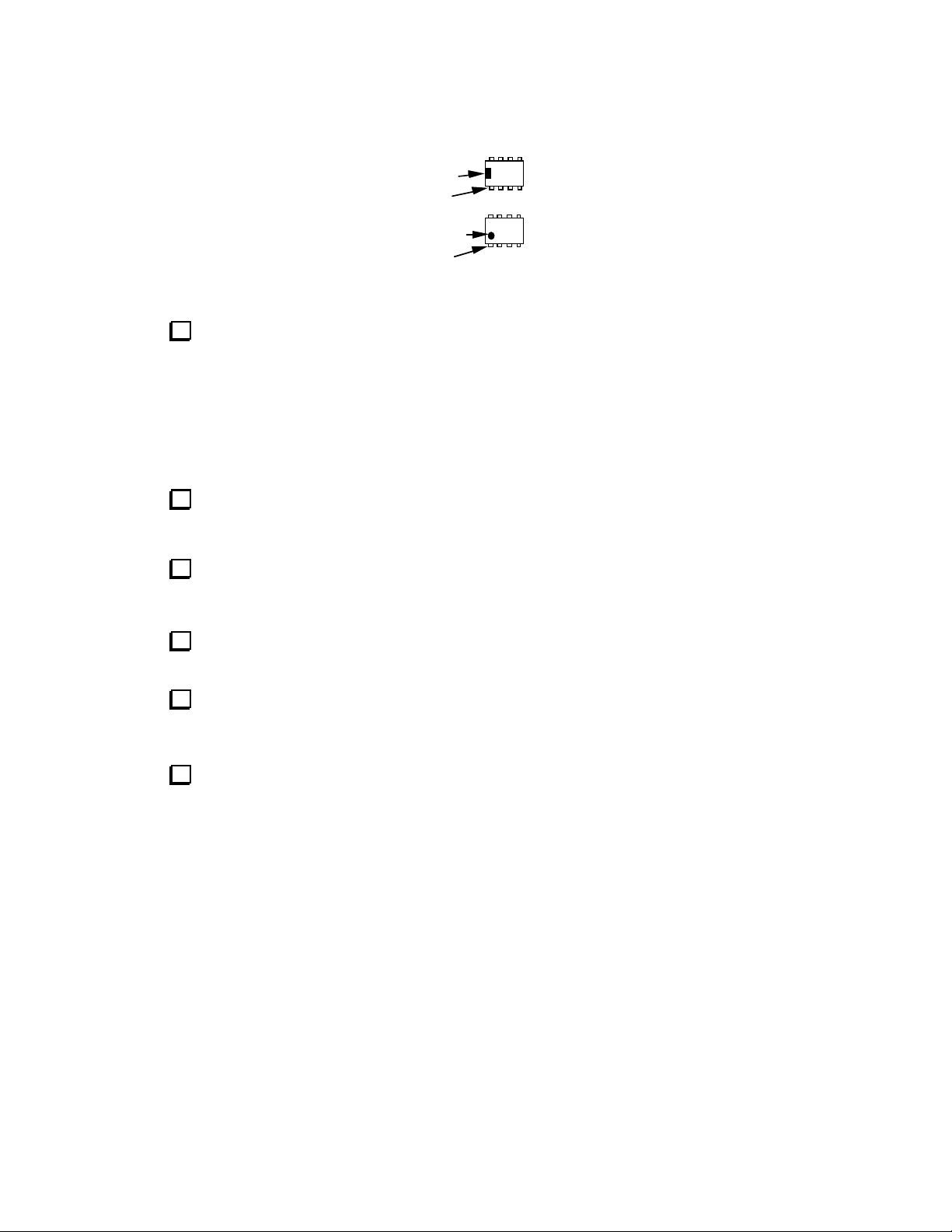
Note: The pin 1 end of ICs can be identified by a notch or dimple as shown in Figure 1. This end
must be oriented toward the notched end of the component outline.
Pin 1
Notch
Pin 1
Dimple
Figure 1
Install the following ICs on the top side of the board. Orient the notched or dimpled end
toward the notched end of their PCB outline (pin 1 end, to the left). Double-check the orientation
before soldering. Be sure to flush-trim the leads of each IC after soldering so as not to interfere
with cables on the bottom side of the board.
__U4 UCN5891A
__U5 UCN5891A
__U6 TPIC6595
__U7 TPIC6595
Install the rectangular Green LED at DS1 on the top side of the board. Spacing the LED
about 1/8” (3 mm) above the board will nicely align the top of the LED with the case top. The dot
marked on the PCB next to DS1 indicates the placement for the longest lead of the LED.
Visual Inspection: Using a magnifying glass, examine the entire board for unsoldered pins,
solder bridges, broken leads, or backward diodes or ICs. Reheat any suspect joints This simple
check could save you hours of troubleshooting later.
The following components will be installed on the bottom side of the circuit board. Turn over
the circuit board to install the components.
Install 1N4007 diodes at D2 and D3 on the bottom side of the PCB. Make sure the cathode
(banded end) of the diode matches the silk-screened outline on the PCB.
__D2, __D3
Install a 4.7k, 1/8 watt (yel-vio-red) resistor at D1 on the bottom side of the PCB. The
resistor replaces a small diode that was previously used in this position.
Page 10

10
Install 10k, 1/4 watt resistors (brn-blk-org) at R2 and R11 on the bottom side of the PCB.
__R2, __R11
Install the 40-pin IC socket at U1 on the bottom side of the board. The notched end should
be oriented toward the notched end of the PCB outline (pin 1 end, to the left). Solder just two
corner pins. If the socket is not sitting completely flat against the PC board, reheat these two pins
one at a time, pushing the socket down until it snaps into position. Then solder the remaining pins
of the socket.
Install U2, (MAX1406CPE or LT1039CN16) on the bottom side of the PCB. Orient the
notched or dimpled end toward the notched end of their PCB outline (pin 1 end, to the left).
Double-check the orientation before soldering. There is no need to trim the leads of U2.
Install resistor network RP1, 390 ohms (391), 8 pins, on the bottom side of the PCB. This
resistor network is symmetrical and can be installed in either orientation, but for consistency you
should orient it with the pin 1 end (black dot) toward pin 1 of the PCB outline (round pad, also
labeled "1").
Install resistor network RP2, 47k (473), 8 pins, on the bottom side of the PCB. This resistor
network should be oriented with the pin 1 end (black dot) toward pin 1 of the PCB outline (round
pad, also labeled "1").
Install low-profile crystal X2 on the bottom side of the PCB. This is a
short
16.289 MHz
device. Make sure it is flat against the board before soldering. Use a minimum of solder so that it
does not wick through and cause a short on the opposite side of the PCB..
Locate the ground pad near X2. Insert a discarded component lead through this pad, then fold
it over the top of X2. Solder this lead at the ground pad, then solder it to the crystal can. Avoid
overheating the crystal.
Install electrolytic capacitor C15 (10 µF) on the bottom side of the PCB. The (+) lead of C15
must be installed in the hole marked "+". The (+) lead is usually longer than the (-) lead. The (-)
lead is identified by a stripe on the body of the capacitor.
Install transistor Q1 (J310) as indicated by its outline on the bottom side of the PCB. The
installed height of the transistors must be no more than 3/8" (9 mm). The top of Q1 must be no
higher than the top of C15. Use a minimum of soldering time (1-2 seconds per lead).
Page 11
11
Install the subminiature DPDT slide switch S5 on the bottom side of the PCB. Make sure the
switch is firmly seated against the board when soldering. After installing the switch, move its
handle to the position closest to J2.
Install a 16-pin dual-row header at W1-W8 on the bottom side of the PCB. The short pins
are inserted into the PCB. The header must be firmly seated against the board when soldering.
Install a 16-pin dual-row header at W12-W19 on the bottom side of the PCB. The short pins
are inserted into the PCB. The header must be firmly seated against the board when soldering.
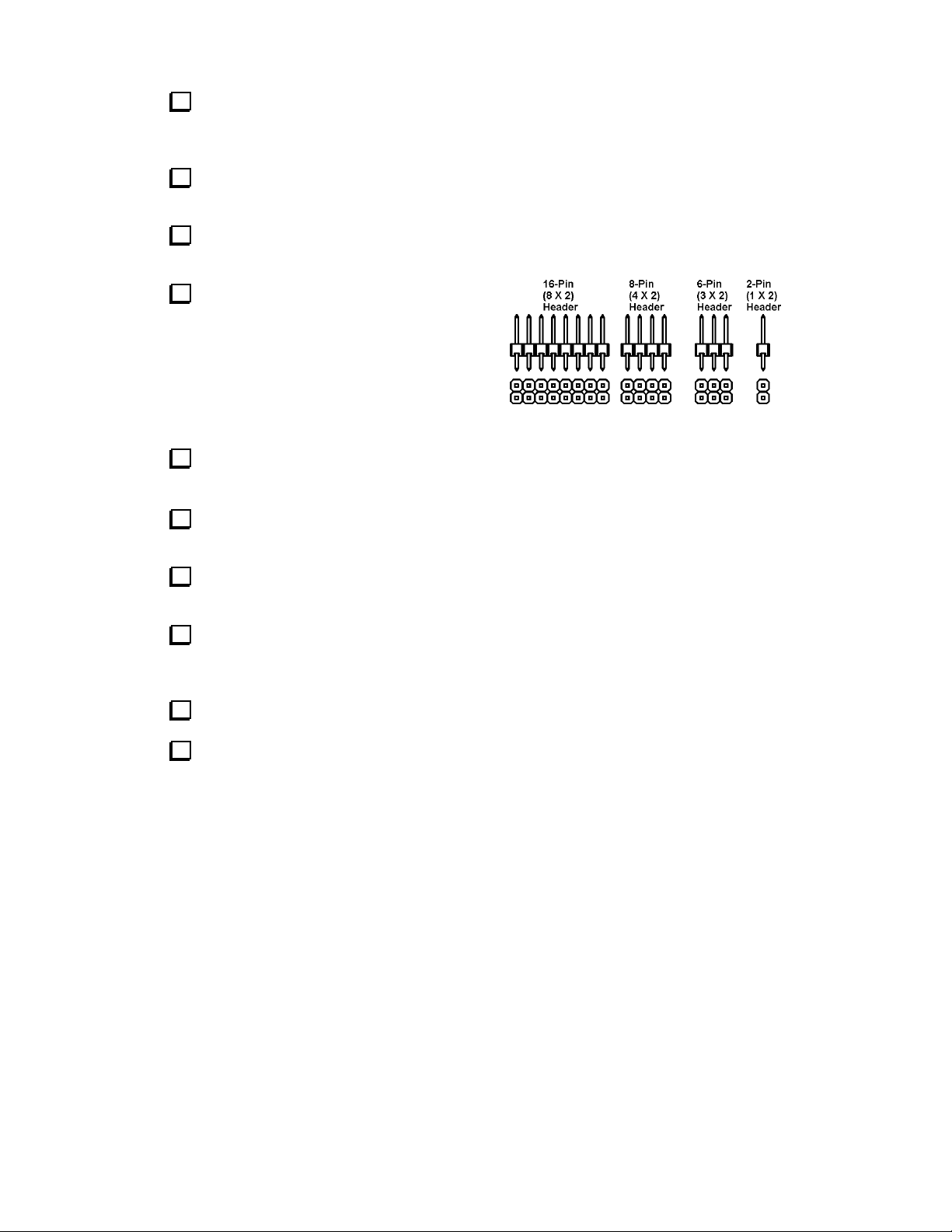
Locate the remaining 16-pin dual-row header.
Cut the header into three pieces so that you have one
8-pin dual row header, a six-pin header and a 2-pin
header. This is best done using diagonal cutters. Cut
the header on the side, then bend the portion to be
cut off away from the rest of the header. The two
pieces should snap apart somewhat cleanly. Discard
the 2-pin header.
Install the 8-pin dual-row header at W20-W23 on the bottom side of the PCB. The short pins
are inserted into the PCB. The header must be firmly seated against the board when soldering.
Install the 6-pin dual-row header at W9-W11 on the bottom side of the PCB. The short pins
are inserted into the PCB. The header must be firmly seated against the board when soldering.
Locate the shorting headers. Install 14 shorting headers on the dual-row headers W9-W19
and W21-W23 by plugging them onto the header pins. Do not install a jumper at W20 at this time.
Install electrolytic capacitor C12 (220 µF) on the bottom side of the PCB. The (+) lead of
C10 must be installed in the hole marked "+". The (+) lead is usually longer than the (-) lead. The
(-) lead is identified by a stripe on the body of the capacitor.
Install the DC barrel jack (J3) on the bottom side of the PCB.
Install J2, a male PC-mount DB9 connector on the bottom side of the PCB. This position is
next to the side of the PCB. The connector will “snap” into the board as its mounting tabs “grab”
the board. Be sure you have installed the MALE connector (with pins) before soldering the
connector pins onto the board.
Figure 2
Page 12

12
Install J1, a female PC-mount DB9 connector on the bottom side of the PCB. This position is
approximately in the center at the end of the PCB. The connector will “snap” into the board as its
mounting tabs “grab” the board. Be sure you have installed the FEMALE connector (with sockets)
before soldering the connector pins onto the board.
Refer to Figure 3, and install screw
terminal connectors at J4 and J5 on the
bottom side of the PCB. The opening
between the connectors forms a “trough” for
control cables to external devices. The
terminals must be mounted so their side
openings face this trough. Make sure the feet
of the terminals are firmly seated against the
board, leaving a very slight gap between the
body of the terminal and the PCB.
__J4, __J5
Connect two terminals together end-to
end by sliding the tab of one connector into
the slot of another. This forms a single 8-pin
connector. Form three other eight-pin
terminals following the same procedure, then
install the screw terminals at the locations
indicated in Figure 3 on the bottom side of
the PCB. Make sure the terminals are
mounted so their side openings face the
trough. Also make sure the feet of the
terminals are firmly seated against the board,
leaving a very slight gap between the body of
the terminal and the PCB.
__J6/J8 __J7/J9,
__J10/J12, __J11/J13
Install crystal X1, a
tall
, 4.000 MHz
device, on the bottom side of the PCB. Make sure it is flat against the board before soldering. Use
a minimum of solder to avoid the solder wicking through to the other side, causing a short.
Locate the ground pad near X1. Insert a discarded component lead through this pad, then fold
it over the top of X1. Solder this lead at the ground pad, then solder it to the crystal can. Avoid
overheating the crystal.
Figure 3
Page 13

13
Adjacent to J1, on the bottom side of the board, you will find two pads connected by a white
line. Using one of the 1N4007 diode leads previously saved, install a 1/4" (6 mm) tall U-shaped
ground jumper between these two pads, on the bottom side of the board. This jumper can be used
as a ground point for test instruments.
Locate the remaining three pushbutton switches. These will now be installed on the top side
of the board. Insert the switches into their mounting holes at S2, S3 and S4, spreading the legs
slightly so they will properly engage the holes. Press the switch down until it is fully seated on the
bends in its leads. There will be a slight gap between the switch body and PCB. Solder the
switches onto the circuit board from the top side.
__S2, __S3 __S4
Locate the four pushbutton key caps. Making sure the key caps are oriented from end-to-end
across the board, press the key caps onto the pushbutton switch stems until they lock into place.
i
Before handling U1, touch an unpainted, grounded metal surface.
i
When you install the IC in the following step, always straighten the leads of the IC first as
shown in Figure 4. The two rows of pins must be straight and parallel to each other to establish the
proper pin spacing for insertion into the PC board or socket. To straighten the pins, rest one entire
row of pins against a hard, flat surface. Press down gently on the other row of pins and rock the IC
forward to bend the pins into position as shown below.
Straight
Flared
Figure 4
Carefully straighten the pins on the microcontroller, U1 (PIC16F877A). The two rows of pins
must be parallel to each other, with no pins bent.
Press the microcontroller into its socket, orienting the notched or dimpled end of the IC with
the notched end of its component outline. The labeling on the microcontroller should read from
left to right.
This completes assembly of the KRC2 circuit board. There are two remaining parts locations, R5
and SP1, which are used with the accessibility speaker option. All other component locations
should now be filled.
Page 14

14
Visual Inspection: Using a magnifying glass, examine the entire board for unsoldered pins,
solder bridges, broken leads, or backward diodes or ICs. Reheat any suspect joints This simple
check could save you hours of troubleshooting later.
Case Assembly
Locate the case top cover. This piece has three rectangular holes punched into the face.
Locate a 4-40 x 3/16” flat head screw. Push it through the hole on the top of the case, holding
it in place with a finger as you turn the case over. Locate two #4 internal-tooth lock washers. Slide
both lock washers onto the screw shaft inside the case. Locate the 1/4 x 3/16” round threaded
standoff. While holding the screw with a Philips screwdriver, screw the standoff onto the screw.
Tighten the assembly.
Insert the circuit board assembly into the case with the pushbutton switches and LED passing
through the rectangular holes in the case. Secure the circuit board to the case with a single 4-40 x
3/16” pan head Philips screw and #4 lock washer.
Locate the four #4 male-female hex standoffs. These are used to secure the DB9 connectors
to the case. Screw each standoff through one of the mounting holes next to the DB9 connectors in
the end of the case into the threaded DB9 assemblies.
Locate the two “2-D” fasteners. These are used to secure the
case top and bottom. Note that on the side of the fastener with
two screw holes, there is more space to one side of the holes than
the other. The side with the most space will face away from the
circuit board.
Using two 4-40 x 3/16” flat-head screws, attach one “2-D”
fastener to the case top just above the J1 DB9 connector. Make
sure the wide side of the fastener side faces away from the circuit
board.
Attach the second “2-D” fastener, using two 4-40 x 3/16” flat head screws, to the end of the
top case away from the DB9 connectors. Follow the same procedure as in the previous step.
Again, the wide side of the fastener should face away from the circuit board.
Figure 5
Page 15

15
KRC2 Test Procedure
The KRC2 should be powered from its DC barrel jack using a +12 volt supply for its initial
power-up. No other connections should be made to the unit.
Connect the power source to the unit. After a short delay while the KRC2 performs
diagnostics, the front-panel LED should turn on to its dim level. If this does not happen, turn
power off to the unit and refer to the troubleshooting section.
Driver Relay Test: You will need a DC voltmeter for this procedure. Connect the black lead
(common) to the ground jumper located near J1 on the KRC2. The red lead should be used to
measure the voltage on each terminal of J6, J7, J8 and J9. Be sure to check the voltage at the side
connector of each terminal. The initial readings should be 0 volts on each terminal.
The Tap/Hold Rule: Each of the pushbutton switches on the front panel has two functions, one
activated by a TAP (short press) and the other activated by a HOLD (long press, about 1/2
second). To highlight this in the text, we use two different typographical styles to identify
switches: T AP and H OLD .
Holding
should cause the KRC2 to change the driven band terminal. Only the 60m source
terminal should indicate 12 volts. The LED should be alternating between dim and bright.
Holding
again should cause the 10m source terminal to indicate 12 volts, and all others to
remain off.
Continue this procedure, actuating the
command until all HF source terminals have been
checked.
The
function is used to switch the AC1-AC3 outputs. First, hold
,
then tap
F1.
The
AC1 source terminal should now indicate +12V and AC2 and AC3 source terminals indicate 0V.
Hold
,
then tap
F2.
The AC2 source terminal should now indicate 12V with AC1 and AC3
at 0 V.
Hold
,
then tap
F3.
The AC3 source terminal should now indicate 12V with AC1 and AC2
at 0 V.
Hold
,
then tap
F4.
All three AC source terminals should now indicate 0 volts.
This completes checkout of the KRC2. Continue to the Final Assembly section.
Page 16

16
KRC2 Final Assembly
Place the case bottom onto the case top, aligning the screw holes at each end of the case. The
case may be a tight fit, but the two halves should slide into place without difficulty.
Using two 4 x 3/16” pan-head screws, secure the case bottom to the top.
Locate the four rubber stick-on feet. Remove the adhesive backing from each foot, and place
the foot securely into place in a corner of the case bottom about 1/8” in from each side.
K2 to KRC2 Control Cable Assembly
Locate the 8-conductor cable. Note: A shorter cable may be used as long as it accommodates
the physical orientation of the K2 and the KRC2. A longer cable can also be used, but it will have
to be tested to ensure that it is not subject to RF interference. A more heavily-shielded control
cable may be required. A standard shielded male-female DB9 straight-through cable has been
tested and should work well with the KRC2/K2 combination.
Remove 1/2" (12 mm) of the jacket from the cable at each end. Be very careful not to nick
the individual wires.
Peel back and cut away the foil shield.
Strip 3/16" (5 mm) of insulation from each insulated wire.
Twist the strands of each wire together. Tin lightly with solder.
Locate the male and female DB9 connectors.
Insert the female DB9 connector (KRC2 end) into the vise, with the solder cups facing up.
Solder the wires to the indicated connector pins at the KRC2 end of the cable as shown in
Figure 6. It may be helpful to melt some solder into each solder cup on the connector first.
Pin 1 Bare wire Pin 2 Orange Pin 3 Blue
Pin 4 Red w/ Black stripe Pin 5 White w/ Black stripe Pin 6 Green
Pin 7 White Pin 8 Red Pin 9 Black
Page 17

17
Figure 6
Remove the female connector from the vise (K2 or K2/100 end), and insert the male
connector (KRC2 end). Solder the wires to this connector using the same colors and pins as in the
previous step.
Locate the connector housing (backshell) and associated hardware.
Note: A single hinged backshell may be provided rather than a two-piece backshell.
Attach a backshell to the male connector at the
K2 or K2/100 end of the cable. Figure 7 shows how
the backshell appears when assembled. Use the
provided cable clamp to hold the cable in position,
then secure the clamp with two screws. The
jackscrews must be retained by the shells. Secure
the backshell halves with the provided hardware (or,
if the shell is hinged, snap the backshell closed). Do
not over-tighten the two screws which secure the
cable clamp!
Attach the remaining backshell to the female
connector at the KRC2 end using the procedure
described above.
Figure 7
Page 18

18
Using the KRC2
The features described in this section are available with KRC2 firmware version 1.5 and later.
Please see earlier revisions of this manual for operation with previous firmware versions.
KRC2 operation with an Elecraft K2 or K2/100 Transceiver
The KRC2 should be connected to the K2 using the Male/Female DB9 cable assembly described
in the previous section. The KRC2 derives its operating power from the K2 in this configuration.
In the KRC2's factory configuration, the per-band outputs (both sink and source) will be turned on
or off based on the K2's selected band. This default behavior will suffice for many amateur station
applications. However, the correspondence between selected band and output driver states is fully
programmable. Band mapping and other configuration changes are accomplished using the KRC2
configuration utility, available from the Elecraft web site (www.elecraft.com). For example, if the
station includes a 20/15/10 meter tri-band beam, the 20 m sink output could be programmed to be
turned on whenever the K2 is set for 20, 15, or 10 meters. Another alternative for mapping
multiple bands to a single antenna or other device is to "wire-OR" the outputs. This is explained in
more detail later in the manual.
Switch S5, accessible through a small hole in the side of the KRC2 sets the operational mode of
the unit. For normal operation, the OP (operate) position of S5 is used. This allows the KRC2 to
communicate with the K2 via its AuxBus and RS-232 interfaces. Set S5 to the DL (Download)
position for downloading firmware upgrades or device configurations to the unit. Firmware
upgrades can be downloaded using the KRC2 download utility, available from the Elecraft web
site.
Page 19

19
Default Key Behavior
There are four buttons on the top of the KRC2, labeled F1, F2, F3 and F4. In the KRC2's factory
configuration, the F1-F4 buttons have the following TA P and H OL D functions:
F 1 Sends the contents of K2 CW message buffer #1.
F 2 Sends the contents of K2 CW message buffer #2.
F 3 Sends the contents of K2 CW message buffer #3.
F 4 Sends the contents of K2 CW message buffer #4.
Note: Playing messages using F 1 - F 4 is more convenient than using the K2’s
FAST PLAY (1-touch) technique.
F 1 Selects the next lower HF band’s relay driver output in the KRC2.
F 2 Selects the next higher HF band’s relay driver output in the KRC2.
Note: This is useful in cases where you switch to a K2 band for which no antenna
relay has been connected in the KRC2. See next page for details.
F 3 Switches the K2 receiver to (or from) the RCV ANT jack. This is a toggle operation.
F 4 Holding this button, then tapping any button, will then cause one of the ACC drivers
to be turned on or off as shown in the list below. The KRC2 will illuminate the green
LED at full brightness while it is awaiting the key tap.
F 1 Turn on AC1 driver.
F 2 Turn on AC2 driver.
F 3 Turn on AC3 driver.
F 4 Turn OFF all ACC drivers.
Note that holding F 4 instead of tapping a key will cancel the function.
The F 1 and F 2 functions change the output terminal for the relay drivers up or down in single
band increments. When the highest band is selected, the next hold of F 2 will cause the drivers to
go to the 160m setting. Conversely, when the lowest band is selected, the next usage of the F 1
function causes the drivers to go to the highest band. The band map follows the values indicated in
Table 5, which places the 60m band above the 10m band. Thus the sequence will be:
…12m<->10m<->60m<->160m<->80m<->40m… While the selected driver is different from the
current band indicated by the transceiver, the green LED will flash between dim and bright states.
The XVT drivers do not participate in the sequence, and when the transceiver selects a transverter
these buttons will not change the driver selection.
Page 20

20
KRC2 Jumper Configuration
There are 21 jumpers in the KRC2 allowing for a wide range of device options. The W1-8 block,
located near the front of the case, controls device configuration for different radio setups and
driver output logic. Table 1, Table 2 and Table 3 show the different settings.
Jmpr
Jumper Out (default)
Jumper In
W1
Use digital band decoding
Use analog band decoding
W2
Band decode option bit 1 - see Table 2
Band decode option bit 1 - see Table 2
W3
Band decode option bit 2 - see Table 2
Band decode option bit 2 - see Table 2
W4
ACn drivers use 1 of 3 decoding
ACn drivers use binary coding
W5
Xvtr drivers use 1 of 3 decoding
Xvtr drivers use binary decoding
W6
No auto-report mode
Place XCVR in auto-report mode
W7
Data Rate bit 0 – see Table 3
Data Rate bit 0 – see Table 3
W8
Data Rate bit 1 – see Table 3
Data Rate bit 1 – see Table 3
Table 1
W1W2W3
Band decode source
Out
Out
Out
AuxBus Mode – K2 operation
Out
OutInSerial Port Mode – K2 or Kenwood operation
OutInOut
Digital Input through J4
OutInIn
Not used
In
Out
Out
Analog input using ALC input (DB9 pin 4)
In
OutInAnalog input using 8R input (DB9 pin 9)
InInOut
Analog input using VRDET input (DB9 Pin 7)
InInIn
Analog input using 8R input (DB9 pin 9) with
reference voltage on ALC input (DB9 pin 4)
Table 2
W8W7Data Rate
Out
Out
4800
OutIn9600
In
Out
19200
InIn4800
Table 3
Page 21

21
Jumpers W4 and W5 determine the bandmap used for outputting band data. For normal use they
should be removed. The KRC2 Configuration tool allows the bandmaps to be edited by the user.
Jumpers W4 and W5 may be used in conjunction with the Configuration tool remapping in order
to allow alternate or extended output configurations. See the KRC2 Configuration Tool
documentation for more information.
Jumpers W9-W23 are used to connect or disconnect the DB-9 connectors from the KRC2.
Normally these jumpers should be left installed. When used with a K2, the minimum jumpers that
must be installed in this block are W16, 18, 19, 21 and 23. DO NOT install jumper W20 when
using the KRC2 with the K2. Doing so will cause problems in the K2, including disabling SSB
output. If the PC connector (J1) is used to pass K2 information through to a peripheral such as a
KAT100, it is important that all jumpers in the W9-W23 block with the exception of W20, be
installed.
Jmpr
Connector
Discussion
W9
J1 Pin 2 - PC
Enables Serial Data to PC from KRC2 or XCVR.
W10
J1 Pin 3 - PC
Enables Serial Data from PC to KRC2 or through to XCVR.
W11
J1 Pin 4 - PC
Enables J1 Pin 4
W12
J1 Pin 9 - PC
Enables J1 Pin 9
W13
J1 Pin 8 - PC
Enables J1 Pin 8
W14
J1 Pin 7 - PC
Enables J1 Pin 7
W15
J1 Pin 6 - PC
Enables J1 Pin 6
W16
J2 Pin 6 - XCVR
Enables K2 AuxBus signal into KRC2. Must be installed for
KRC2 AuxBus band decode mode operation.
W17
J2 Pin 7 - XCVR
Enables K2 VRDET signal into KRC2.
W18
J2 Pin 8 - XCVR
Enables K2 12CTRL signal into KRC2. This signal normally
powers the KRC2.
W19
J2 Pin 9 - XCVR
Enables K2 8R signal into KRC2. Used to determine
transmit/receive activity in K2 operating mode.
W20
J2 Pin 4 - XCVR
Enables K2 ALC signal into KRC2.
DO NOT insert this jumper when using the KRC2 with the K2!
W21
J2 Pin 3 - XCVR
Enables K2 TxD signal from KRC2 serial port driver.
W22
J2 Pin 3 - XCVR
Enables K2 TxD signal from J1 pin 3 (PC serial port driver).
W23
J2 Pin 2 - XCVR
Enables K2 RxD serial port signal into KRC2.
Table 4
Page 22

22
When the KRC2 is set to receive band data in an analog mode, the jumpers associated with the
selected input should be removed from the J2 connection. The analog input should then be fed into
the KRC2 using the PC connector. Use J1 pin 1 for the ground return connection. These settings
and connections are listed in Table 5.
Analog Input
Remove Jumper(s)
J1 Pin for input
Comments
8R / AN1
W19
9
0 - 10 volt input range
VRDET / AN2
W17
7
0 - 5 volt input range
ALC / AN3
W20
4
0 - 10 volt input range
Table 5
i
Important! Do NOT use the jumper connections to bridge external RS-232
serial port signals. This may cause serious damage to your radio when moving the
KRC2 from one radio to another. The preferred method is to provide the bridging
in the cable used with the radio needing it. This specifically applies to Kenwood
transceivers.
Rig-Specific Setup
The following settings are suggested for each radio. Note that these are suggested that have been
successful for users. Other setups are possible and may be preferred. Note that W4 and W5 should
be set as required for the desired bandmap configuration.
Elecraft K2.
• K2 AuxBus used for band, serial port for control and data. PC logging program in use:
Installed
Removed
W1, W2, W3, W6, W7, W8
W9, W10, W16-W19, W21-W23
W11-W15, W20
• K2 AuxBus used for band, serial port for control and data. Stand-alone (no PC):
Installed
Removed
W6
W1, W2, W3, W7, W8
W9 -W19, W21-W23
W20
• K2 serial port used for band, data and control communications. PC logging program in use:
The KRC2ACC may use this setup for communications with the K2.
Installed
Removed
W3
W1, W2, W6, W7, W8
W9, W10, W16-W19, W21-W23
W11 – W15, W20
Page 23

23
• K2 serial port used for band, data and control communications. Stand-alone (no PC):
The KRC2ACC may use this setup for communications with the K2.
Installed
Removed
W3, W6
W1, W2, W7, W8
W9 -W19, W21-W23
W20
Elecraft K3. The preferred setup for the K3 uses the AuxBus for band communications. This
mode uses the K3’s AuxBus for band communications.. Connect J1/J2 pin 6 to pin 2 of the K3’s
AuxIO connector. J1/J2 pin 1 (Ch Gnd) should be connected to K3 Aux IO pin 5. The KRC2 may
also be connected to the K3’s serial port to determine bands. In this configuration control and data
communications will be functional, however not all K3 commands or data may be recognized by
the KRC2.
• AuxBus. Control and data transfers are not available.
Installed
Removed
W1, W2, W3, W6, W7, W8
W9 -W23
• Serial port, PC Logging in use, data rate set to 19200 bps:
Installed
Removed
W3, W8
W1, W2, W6, W7
W9, W10, W21-W23
W11-W20
• Serial port, (no PC), data rate set to 19200 bps:
Installed
Removed
W3, W6, W8
W1, W2, W7
W9, W10, W21-W23
W11-W20
Kenwood. This mode uses Kenwood’s serial port for control and data communications. The data
rate may be set using the W7 and W8 jumpers as required. See Table 3 for this information. Some
Kenwood radios require the use of RTS/CTS handshaking in order to enable communications. If
this is required with your radio, connect a jumper wire from W14 to W17. The wire should be
connected to the jumper pins nearest the DB-9 connectors.
• PC Log program in use, data rate of 19200 bps
Installed
Removed
W3, W6, W8
W1,W2, W7
W9, W10, W21-W23
W11-W20
• Stand-alone (no PC) operation, data rate of 19200 bps
Installed
Removed
W3, W6, W8
W1, W2, W7
W9, W10, W21-W23
W11-W20
Page 24

24
Icom using analog band data. Here we use the radio’s analog band output for band information.
Control and data transfers are not available. Some Icom radios have shown a tendency for the
band output to drift with increased transmit output power. For this reason it is recommended that
the reference input setup be used. In this configuration, the band data is connected to pin 9 and the
8 volt reference is connected to pin 4. This mode is set with jumpers W1, W2 and W3 installed.
• Analog band input on J1/2 pin 4:
Installed
Removed
W1
W2, W3, W6, W7, W8
W11, W20
W9, W10, W12-19, W21-W23
• Analog band input on J1/2 pin 9:
Installed
Removed
W1,W2
W3, W6, W7, W8
W12, W19
W9 -W11, W13-18, W20-W23
• Analog band input on J1/2 pin 9 with reference voltage on J1/2 pin 4:
Installed
Removed
W1, W2, W3
W6, W7, W8
W11, W12, W19, W20
W9, W10, W13-18, W21-W23
Yaesu FT817 using analog band data. Band is determined from the radio’s analog voltage
output. Control and data transfers are not available
• Analog input on J1/2 pin 7:
Installed
Removed
W1, W3
W2, W6, W7, W8
W14, W17
W9–W13, W15, W16, W18-W23
Computer parallel printer port. BCDband information is communicated using the parallel data
available from some computer’s parallel port or parallel BCD data from some radios. Control and
data transfers are not available
• Parallel PCB information
Installed
Removed
W2
W1, W3, W6, W7, W8
W9–W23
For all analog inputs, use J1 or J2 (same connector as the analog input), pin 1 for ground
connection.
Page 25

25
KRC2 Power Connections
The KRC2 may be powered from one of several sources. The
microcontroller and logic are powered either from the K2 through the
DB-9 connector, or from the +12V DC barrel jack. The voltage
applied at the DC barrel jack must not exceed 15 volts.
Power for the Source drivers can come either from the DC barrel jack
or the J5 terminal connector. Voltage applied to the J5 ‘V’ terminal
must not exceed +50 volts. Maximum current drain for either source is
1 amp.
Connecting the KRC2’s Drivers
There are 36 driver output terminals. The terminals are accessible by
removing two access screws on the bottom case. Sixteen of the drivers
will source current, and another sixteen will sink current. The
remaining four drivers, labeled A, B, C and D, are TTL-compatible
inputs or outputs depending on the operating mode. In normal KRC2
or analog modes, the terminals are outputs. In digital parallel input
mode, they become inputs, and receive the BCD-encoded band data.
An additional four terminals are provided for connecting the KRC2 to
ground returns, and to provide a supply voltage for the source drivers
as described in the KRC2 Power Connections section. Figure 8
illustrates the connections. A bar over the terminal label indicates the
output is a sink driver. Sink driver terminals are located near the front
of the box. Source drivers are located toward the rear of the box.
Like-drivers may be wire-ORed (connected together) in order to allow a relay to be selected on
more than one band. For example, the control line from a tri-band beam would connect to
terminals 20, 15 and 10 for source drivers, or /20, /15 and /10 for sink drivers.
IN NO CASE SHOULD THE SOURCE AND SINK TERMINALS BE CONNECTED
TOGETHER IN ANY WAY!
Connecting other Elecraft Peripherals
Additional Elecraft peripherals, such as a KAT-100 or XV-Series transverter, may be connected to
the KRC2’s PC port in a “daisy-chain” fashion in order to operate with the K2. Simply plug the
DB-9 connector from the peripheral into the KRC2’s PC port, and use the peripheral as if it were
directly connected to the K2. Be sure to follow the rules outlined in the jumper discussion and
insert all jumpers in the W9-W23 block with the exception of W20 when using this configuration.
KRC2 PC Connections
A personal computer’s RS-232 serial port may be connected to the KRC2’s PC port using the PC
connector. Normally the K2 does not automatically report its settings to the KRC2. If you have an
alternate KRC2 configuration that needs for the K2 to report its settings, install jumper W6 to
enable the K2’s auto-report mode.
Figure 8
Page 26

26
Using the KRC2 with non-Elecraft Radios
The KRC2 is designed to accept band information from radios other than the K2. As discussed in
KRC2 Jumper Configuration, setting jumpers W1-3 for Kenwood mode operations allows the
KRC2 to interface with those radios in a manner similar to the K2. Other radios that do not use
this command set may not be interfaced using this mode.
To use the KRC2 with an ICOM transceiver that has analog (stepped voltage) band output, you
should set the W1-3 jumpers for Analog Mode using the desired input (8R/AN1 or ALC/AN3),
and connect the transceiver’s analog output to the appropriate input pin on J1 or J2. Be sure to
remove W19 or W20 as appropriate. Power the KRC2 using an external 12-volt supply connected
to the KRC2’s DC barrel jack. The KRC2 should now set its band outputs according to the voltage
presented by the radio.
The three analog inputs have slightly different characteristics you should consider when choosing
which to use. The 8R/AN1 and ALC/AN3 inputs have voltage divider networks on their inputs
that divide the input by 2. Thus their input range is from 0 to 10 volts. The VRDET/AN2 input has
no divider network, giving it a voltage range of 0 to 5 volts. Each input voltage is filtered through
a band selection table that determines the selected band. There are three tables, one for each input.
The factory-configured tables are set up for Icom radios with voltage range of 0 to 8 volts for the
wide-range inputs, with the third table set for the Yaesu FT-817 transceiver’s analog output. These
tables are user-configurable using the KRC2 Configuration tool
To use the KRC2 with a Yaesu radio or computer parallel port outputs, set jumpers W1-3 as
follows: W1 OUT, W2 IN, W3 OUT as described in Table 2. You may then connect the radio or
computer outputs to the KRC2’s ABCD terminals, with the return ground connected to one of the
terminals labeled ‘G’. Power the KRC2 from an external 12-volt supply connected to the DC
barrel jack. The unit should now switch the driver outputs in accordance to the digital inputs it
sees. Note that in addition to the standard BCD outputs, the KRC2 recognizes additional band
codes according to Table 5.
Binary coding
Hex
Band
Binary coding
Hex
BAND
0001
01
160m
10000812m
00100280m
10010910m
00110340m
10100A60m
01000430m
1011
0B
unused
01010520m
1100
0C
XVT1
01100617m
1101
0D
XVT2
01110715m
1110
0E
XVT3
Table 6
Page 27

27
Troubleshooting
If you have any difficulty with your KRC2:
Most problems in building the KRC2 are caused by poor or non-existent solder joints. Closely
examine the PC board for poor solder joints and incorrect, broken or missing components.
Problem: The KRC2’s LED does not turn on.
Make sure the KRC2 is powered, either from the K2 or from the DC barrel jack. The KRC2 must
be powered from one of these two sources. The internal controller circuits may not be powered
from J5’s ‘V’ terminal.
Problem: Source drivers inoperative.
The source drivers require that a DC supply of up to 15 volts be attached to the KRC2’s DC barrel
jack, or a DC supply of up to 50 volts be connected to terminal ‘V’ of J5. The source drivers are
not capable of supplying voltage from the K2’s power supply.
Problem: KRC2 does not communicate with K2.
Check jumpers W9-W23. All but W20 must be installed for the KRC2 to communicate properly
with the K2. If these are properly installed, check the cable connecting the KRC2 and K2. This
must be a straight-through Male DB9-Female DB9 cable as constructed in this manual.
Problem: K2 has no transmitter output in voice modes.
Remove jumper W20 from the KRC2. The KRC2 adversely affects the K2’s ALC system, causing
low voice power output of the transceiver. The K2 works quite well without the external ALC line
installed, so simply leave jumper W20 out of the KRC2.
Problem: LED Flashing on and off.
On/off LED flashing indicates that the KRC2’s microcontroller has not passed its startup tests, and
is waiting for a firmware download. This is not to be confused with the slower bright/dim LED
flashing which indicates the driver band selection does not match the K2’s band setting. Try
turning power off then on to the unit. If the condition persists, contact Elecraft technical support
for an upgrade.
Included below are complete DC Voltage Tables for all ICs.
Page 28

28
DC Voltage Chart
Voltages are approximate and will vary up to +/- 10% due to normal component variation without
affecting the operation of the KRC2. Measurements were made under the following conditions:
KRC2 powered by K2, K2 powered by a 14.0 V (measured) power supply, K2 powered on, set to
14290.9 MHz. Switch to this band from another after powering on K2/KRC2 combination.
Nothing attached to the KRC2’s DC barrel jack or PC DB9 connectors. No wires attached to the
J4-J13 terminal connectors. Measurements taken with Metex ME-22 Digital Volt Meter.
PinVPinVPinVPinVPin
V
U1 P1
4.75
U1 P27
4.56
U2 P13
4.95
U5 P7
0.00
U6 P17
0.00
U1 P2
2.77
U1 P28
0.00
U2 P14
0.00
U5 P8
0.00
U6 P18
0.00
U1 P3
3.45
U1 P29
4.56
U2 P15
4.95
U5 P9
0.00
U6 P19
0.00
U1 P4
0.00
U1 P30
0.00
U2 P16
4.95
U5 P10
0.00
U6 P20
0.00
U1 P5
0.00
U1 P31
0.00
U4 P1
0.00
U5 P11
0.00
U7 P1
0.00
U1 P6
0.79
U1 P32
4.95
U4 P2
4.95
U5 P12
0.00
U7 P2
4.95
U1 P7
4.93
U1 P33
4.95
U4 P3
4.95
U5 P13
13.35
U7 P3
0.00
U1 P8
5.55
U1 P34
4.95
U4 P4
0.00
U5 P14
0.00
U7 P4
0.00
U1 P9
1.97
U1 P35
4.95
U4 P5
0.00
U5 P15
4.95
U7 P5
0.00
U1 P10
4.63
U1 P36
4.95
U4 P6
0.00
U5 P16
0.00
U7 P6
0.00
U1 P11
4.95
U1 P37
4.95
U4 P7
0.00
U6 P1
0.00
U7 P7
0.00
U1 P12
0.00
U1 P38
4.95
U4 P8
0.00
U6 P2
4.95
U7 P8
4.95
U1 P13
1.77
U1 P39
4.95
U4 P9
0.00
U6 P3
4.95
U7 P9
0.00
U1 P14
2.21
U1 P40
4.95
U4 P10
0.00
U6 P4
0.00
U7 P10
0.00
U1 P15
4.93
U2 P1
12.86
U4 P11
0.00
U6 P5
0.00
U7 P11
0.00
U1 P16
0.00
U2 P2
0.00
U4 P12
0.00
U6 P6
0.00
U7 P12
0.00
U1 P17
4.90
U2 P3
12.42
U4 P13
13.35
U6 P7
0.00
U7 P13
4.95
U1 P18
4.95
U2 P4
-2.52
U4 P14
0.00
U6 P8
4.95
U7 P14
0.00
U1 P19
4.93
U2 P5
-7.56
U4 P15
4.95
U6 P9
0.00
U7 P15
0.00
U1 P20
4.93
U2 P6
-6.80
U4 P16
0.00
U6 P10
0.00
U7 P16
0.00
U1 P21
4.93
U2 P7
12.42
U5 P1
0.00
U6 P11
0.00
U7 P17
0.00
U1 P22
4.93
U2 P8
-7.55
U5 P2
4.95
U6 P12
0.00
U7 P18
0.00
U1 P23
4.93
U2 P9
0.00
U5 P3
0.00
U6 P13
4.95
U7 P19
0.00
U1 P24
4.95
U2 P10
0.00
U5 P4
0.00
U6 P14
0.00
U7 P20
0.00
U1 P25
4.95
U2 P11
4.95
U5 P5
0.00
U6 P15
0.00
U1 P26
4.95
U2 P12
4.95
U5 P6
11.97
U6 P16
0.00
Note: U6 Pins 4, 5, 6, 7, 14, 15, 16, 17 and U7 Pins 4, 6, 7, 14, 15, 16, 17 are floating (not driven)
with no pullup. U6 pin 5 is driven to zero for 14 MHz as shown in the voltage chart.
Page 29

29
Circuit Details
Refer to the schematic diagram, Figure 7 on page 29.
U1 is a PCI 16F877A microcontroller. This device controls the operation of the KRC2. U1
operates at a clock frequency of 4 MHz, as determined by X1. It communicates with relay drivers
U4-U7 using its built-in Serial Peripheral Interconnect (SPI) interface, commanding them to turn
their outputs on or off. Which outputs should be on or off is determined during execution of the
microcontroller’s internal program. It uses band input from the attached radio or computer to
determine which driver output(s) should be enabled.
The MCU receives band information from the attached radio through one of six input channels.
Three channels are analog, using the MCU’s built-in analog to digital converters to measure band
voltages, while the other three are digital in nature. These consist of a BCD parallel input and two
serial inputs. One serial input enables the MCU to participate on the K2’s AuxBus channel, while
the other uses the MCU’s built-in UART serial port to communicate using the Elecraft serial
protocol (similar to the Kenwood serial protocol). Selection of the active input method is made by
setting the W1-W3 jumpers.
The UART serial port uses industry-standard RS-232 voltages. These are switched in the KRC2
using U2, a MAX1406 (or similar) RS-232 interface. U2 requires a negative power supply for its
operation. This is developed using the oscillator and rectifier circuitry of Q1. Q1 and X2 and their
associated components form an oscillator running at 18.289 MHz. Output from this oscillator is
fed to a voltage-doubling rectifier made up of D6, D7, and C15, then fed to U2’s –12V input pin.
The circuit typically provides –7.5 volts, well within the range required by the RS-232
specification.
For analog band operation, the input voltage is connected to the microcontroller’s AN1, AN2 or
AN3 inputs through divider or isolation networks. The AN1 input comes from pin 9 of J1 or J2,
depending on jumper selection. It is reduced by the divider network made up of R6 and R10. The
values for these resistors provide a division by 2, giving the input a maximum range of 0 to +10
volts. The AN3 input is identical to that of AN1, with RR8 and R11 making up the divide-by-2
network. This input comes from J1 or J2 pin 4. AN2 comes from J1/J2 pin 7, and is fed directly to
the MCU input without a voltage divider. Its input range is 0 to +5V.
The KRC2 can communicate with two devices using the RS-232 port, depending on the setting of
S5. In S5’s normal operation position, the KRC2 listens directly to the transceiver’s serial output,
and also can send directly to the radio attached to the XVCR port. Additionally, the RS-232
signals from a computer attached to the PC port (J1) are ORed with the KRC2’s serial port,
allowing it to send, and listen, to the transceiver as well. No protection is provided to keep
transmissions from the KRC2 and PC from colliding on this channel, so care must be taken to
prevent this in the PC and KRC2 operation. The S5’s Download (DL) position enables the
microcontroller to communicate directly with a PC. This is used in downloading configuration and
firmware upgrades to the KRC2.
Page 30

30
C1
C2
VoutVin
Gnd
1 3
2
U3 78L05
C13
C14
+
C12
.1.1220 µF
R3
1K
C20
.1
33
33
Rx
Tx
C16
.01
D7
1N4148
D6
1N4148
+
C15
10 µF
S4
S3
S2
S1
F1
F2
F3
F4
D3 1N4007
C9
C11
C8
C6
C10
L2
L3
L1
8R
R9 100
.001
ALC
0.001
0.001
0.001
0.001
100uH
100uH
100uH
ISD-D
ISD -C
SP1
Piezo Spkr
W5
W4
T2OUT
R2OUT
R1OUT
T1OUT
T3OUT
R3OUT
R2IN
T2IN
T1IN
R1IN
R3IN
T3IN
GND
VCC
VDD
VSS
16121415131110
2
391
8
547
6
U2
12
3
4
5
6
7
8
9
J2
W16
W17
W18
W19
W23
D2
1N4007
J3
DS1
RP 1 12
390
RP 1 56
390
RP 1 78
390
RP 1
34
390
X1
4.0 MHz
X2
G
DS
Q1
D8
C18
L4
J31 0
120
16.289 MHz
1N4148
C19
56
R13 47
C17
.01
15uH
TTL Level
+12V DC Power
MAX140 6
R4 470
R5
5K
(BACK VIEW)
12345
6789
DB-9 Male
Status
8R
VRDET
C3
.001
R6 10K
R7 10K
C4 .001
8R
VRDET
VPP
1
2 3 4
5
6
7 8
9
J1
C7
0.001
(BACK VIEW)
1 2 3 4 5
6 7 8 9
+5V
+5V
+12V
+5V
+5V
+5V
+12V
+5V
DB-9 F emale
PC
C25
.1
R1
R2
10K
47K
2V nominal
-12V
-12V
RxD
TxD
W10
W9
RP 2
14
47K
D5
1N4007
D4
1N4007
W6
W7
W2 W8
W13
W14
W15
W11
W12
8R
12CTRL
12CTRL
AuxBus
AuxBus
ALC
TxD
RxD
SIG GND
SIG GND
CH GND
CH GND
BRL12
BRL12
+12V
GND
VBB
GND
GND
4 3
2
1
J4
4
3 2
1
J5
AUXBU S
AUXBU S
G
S
D
Q1
GND
OUT
IN
U3
D
C
B
A
.01uF each
C21-C2 4
C26
.1
RP 2
13
47K
RP 2
12
47K
RP 2
15
47K
RP 2
16
47K
RP 2
18
47K
RP 2
17
47K
W3
RA5
RA5
OSC1
OSC2
MCLR
AN0
AN1
AN2
RA3
RA4
RA5
RE0
RE1
RE2
VDD
VSS
RC0
RC1
RC2
SCK
RD0
RD1 RD2
RD3
SDI
SDO
RD4
RD5
RD6
RD7
VSS
VDD
RB0
RB1
RB2
RB3
RB4
RB5
RB6
RB7
TX
RX
10
15
20
21
25
30
35
40
PIC16F8 77AU1
5
1
R10 10K
R11 10K
S5A
S5B
Optional
W1
D9
1N4148
D10
1N4148
R12
4.7K
W21
W22
R8 10K
C5
.001
AN3
AN3
Band I/O
MON
MON
OP
DL OP DL
XCVR
VRDET
VRDET
VBB
SDO
SCK
SRWRT
W20
D1 4.7K 1/8 Watt
Figure 9 – KRC2 Schematic
Page 31

31
/SRCLR
SRCK
SOUT
VCC
RCK
SIN
GND
GND
GND
/Q0
/Q1
/Q2
/Q3
/Q4
/Q5
/Q6
/Q7
/G
12
13
19
11
10
14
15
16
17
18
2
9
8
3
4
5
6
7
U6
/SRCLR
SRCK
SOUT
VCC
RCK
SIN
GND
GND
GND
/Q0
/Q1
/Q2
/Q3
/Q4
/Q5
/Q6
/Q7
/G
12
13
19
11
10
14
15
16
17
18
2
9
8
3
4
5
6
7
U7
TPIC65 95
TPIC65 95
C27
.1
Elecraft
Rev. Sht. DateBy
1 of 1
J. Brindle
W. Burdick
KRC2 Remote Control/AuxBox
+5V
Driver Outputs: High-side
GND
CLK
SDI
VBBVDD
SDO
STQ1Q2
Q3
Q4
Q5
10
Q6
11
Q7
12
Q8
1315
16
OE
14
1
2
3
4
5
6
7
8
9
U4
GND
CLK
SDI
VBBVDD
SDO
STQ1Q2
Q3
Q4
Q5
10
Q6
11
Q7
12
Q8
1315
16
OE
14
1
2
3
4
5
6
7
8
9
U5
UCN5891A
UCN5891A
160
80
40
20
15
10
60
30
12
17
XV1
XV3
.01uF each
Driver Outputs: Low-side
/160
/80
/60
/40
/30
/20
/17
/15
/12
/10
/XV1
/XV2
/XV3
.01uF each
C28-C 43
C44-C 59
C60
.1
XV2
AC1
AC2
AC3
/AC1
/AC2
/AC3
4
3
2
1
J6
4
3
2
1
J7
4
3
2
1
J8
4
3
2
1
J9
4
3
2
1
J1 0
4
3
2
1
J1 1
4
3
2
1
J1 2
4
3
2
1
J1 3
SDO
SRWRT
SCK
VBB
C 02/12 /06
Page 32

32
PCB Layout
The corrected PCB layout is shown in Figure 10 for the top side and Figure 9 on page 31 for the
bottom side.
Figure 10 - KRC2 PCB corrected top view / silk screen parts placement
Page 33

33
Figure 11 - KRC2 PCB corrected bottom view / silk screen parts placement.
Page 34

34
Customer Service Information
Technical Assistance
If you have difficulty with kit construction, operation, or troubleshooting, we’re here to help. You
may be able to save time by first consulting our web site, www.elecraft.com, or by posting your
question on our e-mail forum,
elecraft@mailman.qth.net
. Telephone assistance is available
from 9 A.M. to 5 P.M. Pacific time (weekdays) at 831-662-8345. Via e-mail, use
support@elecraft.com for support and parts@elecraft.com to request replacement parts. Please use
e-mail when possible; this gives us a written record of the details of your problem.
Repair Service
If necessary, you may return your completed kit to us for repair. Contact Elecraft before mailing
your kit to obtain current information on repair fees. (Kits that have been soldered using acid core
solder, water-soluble flux solder, or other corrosive or conductive fluxes or solvents cannot be
accepted for repair.) The following information should be provided to expedite repair:
your name, address, and
phone number; your e-mail
address (if applicable); and
a complete description of
the problem.
Shipping: First, seal the
unit in a plastic bag to
protect the finish from dust
and abrasion. Use a sturdy
packing carton with 3" or
more of foam or shredded
paper on all sides. Seal the
package with reinforced
tape. (Neither Elecraft nor
the carrier will accept
liability for damage due to
improper packaging.)
Cover the "to" address label
with clear tape so it will be
weatherproof. Finally, call
or send e-mail to obtain the
proper shipping address.
 Loading...