


K2
E L E C R A F T K 2 T R A N S C E I V E R
F
RCL
BAND
STORE
MENU
EDIT
+
-
DISPLAYBAND
+
RF/ALC
ANT 1/2
+
TUNE
NB
+
LEVEL
+
E L E C R A F T
S1
5 9 +20 40
3 5
RF
KEYER
AF GAIN
7
ALC
RF GAIN
10
POWER
K 2
NB ANT2 PRE ATT A B RIT XIT
T R A N S C E I V E R
0
RATE
LOCK
MODE
+
VOX
PRE/ATT
+
SPOT
RIT XIT
+
PF1
-1
A=BA/B
1
456
CW RV
7
0
AGC
PF2
+1
2
SPLITREV
8
3
XFIL
AFIL
MSG
9
REC
ON
OFF
O W N E R’S M A N U A L
ELECRAFT
®
K2
160-10 Meter
SSB/CW
Transceiver
Owner’s Manual
Revision I, March 29, 2012
Copyright
2012 Elecraft, LLC
All Rights Reserved
Elecraft www.elecraft.com P.O. Box 69 Aptos, CA 95001-0069 (831) 763-4211 Fax: (831) 763-4218

2 ELECRAFT
®
Table of Contents
1. INTRODUCTION .................................................................................................................................................................................. 3
2. SPECIFICATIONS ............................................................................................................................................................................... 5
3. PREPARATION FOR ASSEMBLY ..................................................................................................................................................... 7
4. CONTROL BOARD ........................................................................................................................................................................... 13
5. FRONT PANEL BOARD ................................................................................................................................................................... 23
6. RF BOARD ........................................................................................................................................................................................ 34
7. FINAL ASSEMBLY ............................................................................................................................................................................ 81
8. OPERATION ...................................................................................................................................................................................... 84
9. CIRCUIT DETAILS .......................................................................................................................................................................... 110
10. OPTIONS ......................................................................................................................................................................................... 117
PARTS LIST ............................................................................................................................................................................ APPENDIX A
SCHEMATIC ............................................................................................................................................................................ APPENDIX B
BLOCK DIAGRAM .................................................................................................................................................................. APPENDIX C
PHOTOGRAPHS ..................................................................................................................................................................... APPENDIX D
TROUBLESHOOTING ............................................................................................................................................................. APPENDIX E
PARTS PLACEMENT DRAWINGS ......................................................................................................................................... APPENDIX F
100-WATT STAGE AND RS232 I/O (K2/100) .......................................................... APPENDIX G (SUPPLIED WITH KPA100 OPTION)
Elecraft www.elecraft.com P.O. Box 69 Aptos, CA 95001-0069 (831) 763-4211 Fax: (831) 763-4218

ELECRAFT
®
3
1. Introduction
The Elecraft K2 is a high-performance, synthesized, CW/SSB
transceiver that covers all HF bands. It is a true dual-purpose
transceiver, combining the operating features you’d expect in a
home-station rig with the small size and weight of a rugged,
go-anywhere portable.
The basic K2 operates on 80-10 meter CW, and provides over 10
watts of RF output. If you prefer a full-power station, you can
complete your K2 as a K2/100 at any time by adding the internal
100-watt final stage (KPA100 option). Assembly of the KPA100 is
covered in Appendix G, a separate manual supplied with the
KPA100 kit.
You can customize your K2 by choosing from a wide range of
additional options:
SSB adapter with optimized 7-pole crystal filter
Automatic antenna tuner (20 W internal or 150 W external)
160-m adapter with receive antenna switch
60-m adapter with low-level transverter interface
Computer control interface (RS232)
Noise blanker
Digital or analog audio filter, each with real-time clock
Internal 2.9-Ah rechargeable battery
Programmable band decoder
High-Performance VHF and UHF transverters
For a complete description of available options, see page 117. In
addition to the options, a companion enclosure the same size and
style as the K2 is available for those who wish to build their own
matching station accessories (model EC2).
The K2 is an intermediate-level kit, yet you’ll be pleasantly surprised at
how uncomplicated it is to build. All of the RF (radio-frequency)
circuitry is contained on a single board, while two plug-in modules
provide front panel and control functions. Wiring is minimal, unlike
traditional kits which depend on complex wiring harnesses.
A unique feature of the K2 is that it provides its own built-in test
equipment, including a digital voltmeter, ammeter, wattmeter, complete
RF probe, and frequency counter. These circuits are completed early in
assembly, so they're ready to be used when you begin construction and
alignment of the RF board. We also provide complete troubleshooting
and signal-tracing information.
In addition to this owner’s manual, you’ll find extensive support for the
K2 on our website, www.elecraft.com
are manual updates, application notes, photographs, and information on
new products. There’s also an e-mail forum; sign-up is available from
the web page. It’s a great way to seek advice from the K2’s designers
and your fellow builders, or to tell us about your first QSO using the K2.
We’d like to thank you for choosing the K2 transceiver, and hope it
meets your expectations for operation both at home and in the field.
Wayne Burdick, N6KR
Eric Swartz, WA6HHQ
. Among the available materials
Pre-Wound Toroids Available
You can obtain a set of pre-wound toroids for the K2 if you prefer not to
wind them yourself. Refer to our web site for details.
4 ELECRAFT
®
Customer Service Information
Technical Assistance
You can send e-mail to support@elecraft.com
quickly - typically the same day Monday through Friday. Telephone
assistance is available from 9 A.M. to 5 P.M. Pacific time (weekdays
only) at 831-763-4211. Please use e-mail rather than calling when
possible since this gives us a written record of the details of your
problem and allows us to handle a larger number of requests each
day.
Repair / Alignment Service (We want to make sure
everyone succeeds!)
If necessary, you may return your Elecraft product to us for repair or
alignment. (Note: We offer unlimited email and phone support to get
your kit running, so please try that route first as we can usually help
you find the problem quickly.)
IMPORTANT: You must contact Elecraft before mailing your
product to obtain authorization for the return, what address to ship it
to and current information on repair fees and turnaround times.
(Frequently we can determine the cause of your problem and save
you the trouble of shipping it back to us.) Our repair location is
different from our factory location in Aptos. We will give you the
address to ship your kit to at the time of repair authorization.
Packages shipped to Aptos without authorization will incur an
additional shipping charge for reshipment from Aptos to our repair
depot
.
To ship the unit, first seal it in a plastic bag to protect the finish. Use
a sturdy packing carton with at least 3-in (8 cm) of foam or shredded
paper on all sides. Seal the package with reinforced tape. (Neither
Elecraft or the carrier will accept liability for damage due to
improper packaging.)
and we will respond
Elecraft 1-Year Limited Warranty
This warranty is effective as of the date of first consumer purchase (or if
shipped from the factory, the date the product is shipped to the customer). It
covers both our kits and fully assembled products. For kits, before requesting
warranty service, you should fully complete the assembly, carefully
following all instructions in the manual.
Who is covered: This warranty covers the original owner of the Elecraft
product as disclosed to Elecraft at the time of order. Elecraft products
transferred by the purchaser to a third party, either by sale, gift, or other
method, who is not disclosed to Elecraft at the time of original order, are not
covered by this warranty. If the Elecraft product is being bought indirectly
for a third party, the third party’s name and address must be provided at time
of order to ensure warranty coverage.
What is covered: During the first year after date of purchase, Elecraft will
replace defective or missing parts free of charge (post-paid). We will also
correct any malfunction to kits or assembled units caused by defective parts
and materials. Purchaser pays inbound shipping to us for warranty repair; we
pay shipping to return the repaired equipment to you by UPS ground service
or equivalent to the continental USA and Canada. For Alaska, Hawaii, and
other destinations outside the U.S. and Canada, actual return shipping cost is
paid by the owner.
What is not covered: This warranty does not cover correction of kit
assembly errors. It also does not cover misalignment; repair of damage
caused by misuse, negligence, battery leakage or corrosion, or builder
modifications; or any performance malfunctions involving non-Elecraft
accessory equipment. The use of acid-core solder, water-soluble flux solder,
or any corrosive or conductive flux or solvent will void this warranty in its
entirety. Also not covered is reimbursement for loss of use, inconvenience,
customer assembly or alignment time, or cost of unauthorized service.
Limitation of incidental or consequential damages: This warranty does
not extend to non-Elecraft equipment or components used in conjunction
with our products. Any such repair or replacement is the responsibility of the
customer. Elecraft will not be liable for any special, indirect, incidental or
consequential damages, including but not limited to any loss of business or
profits.

ELECRAFT
®
5
2. Specifications
All measurements were made using a 14.0 V supply and 50-ohm load
unless otherwise indicated. Values are typical; your results will be
somewhat different. Specifications are subject to change without
notice. (See option manuals for additional specifications.)
General
Size
Cabinet 3.0" H x 7.9" W x 8.3" D
(7.5 x 20 x 21 cm)
Overall 3.4" H x 7.9" W x 9.9" D
(8.5 x 20 x 25 cm)
Weight 3.3 lbs. (1.5 kg), excluding options
Supply voltage 9 to 15 VDC;
reverse-polarity protection;
internal self-resetting fuse
Current drain,
Receive 120-150 mA in minimum-current
configuration; 180-250 mA typical
Transmit
1
2.0 A typical at 10 watts;
programmable current limiting
Frequency ranges,2 MHz
Basic kit 3.5-4.0, 7.0-7.3,
10.0-10.2, 14.0-14.5, 18.0-18.2,
21.0-21.6, 24.8-25.0, 28.0-28.8
160 m (opt.) 1.8-2.0
60 m (opt.) 5.0-5.5
VFO
Stability < 100 Hz total drift typ. from
cold start at 25° C
3
Accuracy
+/- 30 Hz over a 500 kHz range
(typ) when calibrated
Resolution 10 Hz
Tuning steps 10 Hz, 50 Hz, and 1000 Hz nominal
(other step sizes available via menu)
Memories 20 (10 assigned to 160-10 m
Bands; 10 general-purpose)
RIT/XIT range +/- 0.6 to +/- 4.8 kHz (selectable);
10-40 Hz steps depending on range.
Fine RIT mode steps 2-3 Hz typ.
Frequency control PLL synthesizer w/single VCO
covering 6.7-24 MHz in 10 bands;
fine steps via DAC-tuned reference
1
Current varies with band, supply voltage, configuration, and load
impedance. We recommend a minimum 3.5-amp power supply.
2
The K2 can receive well outside the indicated bands, but this extended range
is not specified or guaranteed. Transmit ranges may be limited for export to
some countries. The K2/100 (KPA100 option) limits transmit from 25-27.999
MHz to 10 watts or less.
3
See Frequency Calibration Techniques (page 105).

6 ELECRAFT
®
Transmitter
Power output range <0.5 W to >10 W (typ.);
power setting resolution 0.1 W,
accuracy 10% @ 5 W
Min. supply voltage 9.0 V min for 2 watts out
recommended
10.0 V min for 7 watts out
10.5 V min for 10 watts out
Duty cycle 5 W, 100%; 10 W, 50%
Spurious products -40 dB or better @ 10 W (-50 typ)
Harmonic content -45 dB or better @ 10 W (-55 typ)
Load tolerance 2:1 or better SWR recommended;
will survive operation
T-R delay approx. 10 ms-2.5 sec, adjustable
External keying 70 WPM max.
4
9.5 V min for 5 watts out
into high SWR
Receiver
Preamp On Preamp Off
Sensitivity (MDS) -135 dBm -130 dBm
Dynamic range,
I.F. 4.915 MHz (single conversion)
Audio output 1 watt max. into 4-ohm load
rd
3
-order intercept 0 to +7.55 +10
nd
2
-order intercept +70 +70
Blocking 125 dB 133 dB
Two-tone 96 97
Selectivity,
CW 7-pole variable-bandwidth crystal
filter, approx. 200-2000 Hz
6
7-pole fixed-bandwidth crystal
SSB
filter, 2.2 kHz typ.
Speaker internal: 4 ohm, 3 W;
CW sidetone 400-800 Hz in 10 Hz steps
Keyer
Keying modes Iambic A and B; adjustable weight
Speed range 9 - 50 WPM
Message memory 9 buffers of 250 bytes each; 1-level
chaining; auto-repeat (0 - 255 s)
4
For reference only; not guaranteed. If higher power than shown here is to be
used for a given supply voltage, monitor transmitter output signal.
Rear-panel jack for external speaker
Headphones 4 - 32 ohms, stereo or mono
5
Varies with band.
6
With optional SSB adapter. Other CW and SSB fixed crystal filter options
may be available
ELECRAFT
®
7
3. Preparation for Assembly
Overview of the Kit
The K2 uses modular construction, both physically and electrically.
This concept extends to the chassis (Figure 3-1). Any chassis element
can be removed during assembly or troubleshooting. (Also see photos
in Appendix D.) If the KPA100 is installed, it takes the place of the
original top cover.
Side
Panel
Top Cover
Heat
Sink
Front
Panel
Bottom
Cover
As shown in Figure 3-2, there are three printed circuit boards (PCBs)
in the basic K2 kit: the Front Panel board, Control Board, and RF
board. Option modules plug into the RF or Control board, but are not
shown here.
RF
Control
Front
Panel
(Right side panel
not shown)
Figure 3-2
Figure 3-1
8 ELECRAFT
Board-to-board Connectors
The circuit boards in the K2 are interconnected using board-to-board
connectors, which eliminates nearly all hand wiring. Gold-plated
contacts are used on these connectors for reliability and corrosion
resistance.
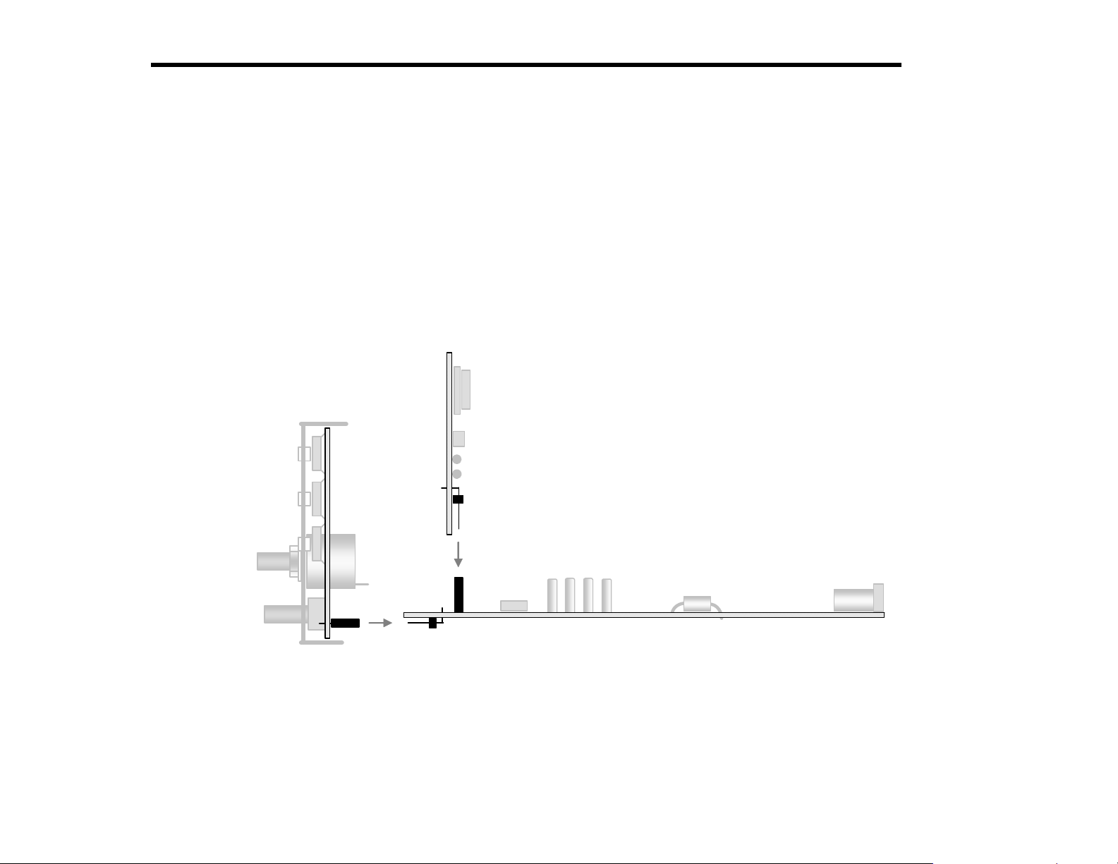
Figure 3-3 shows a side view of the PC boards and board-to-board
connectors. As can be seen in the drawing, the Front Panel board has a
connector J1 which mates with right-angle connector P1 on the RF
board. Similarly, right-angle connector P1 on the Control Board mates
with J6 on the RF board. (Not shown in this drawing are two
additional right-angle connectors on the Control board, P2 and P3,
which mate with J7 and J8 on the RF board.)
These multi-pin connectors are very difficult to remove once
soldered in place. Refer to Figure 3-3 during assembly to make
sure you have each connector placed correctly before soldering.
®
Front Panel
Control Board
P1
RF Board
J6
J1
P1
Figure 3-3

ELECRAFT
®
9
There are six steps in the K2 assembly process:
1. Control Board assembly
2. Front Panel Board assembly
3. RF Board assembly and test, part I (control circuits)
4. RF Board assembly and test, part II (receiver and synthesizer)
5. RF Board assembly and test, part III (transmitter)
6. Final assembly
This assembly sequence is important because later steps build on the
previous ones. For example, in step 3 you’ll put the modules together
for the first time, allowing you to try out the K2’s built-in frequency
counter. The counter will then be used in step 4 to align and test the
receiver and synthesizer on 40 meters. In step 5 all the pieces will
come together when you complete the transmitter and filters, then
align the K2 on all bands. The last few details—speaker, tilt stand,
etc.—will be wrapped up in step 6.
Unpacking and Inventory
When you open the kit you should find the following items:
six chassis pieces (Figure 3-1)
three printed circuit boards (Figure 3-2)
FRONT PANEL board components bag
CONTROL board components bag
RF board components in two bags
MISCELLANEOUS components bag (includes hardware)
WIRE bag
4-ohm Speaker, 5 small knobs, and large tuning knob
plastic tube containing the latching relays
an envelope containing the LCD bezel, green LED bargraph filter,
serial number label, thermal insulators, and other items
Inventory
We strongly recommend that you do an inventory of parts before
beginning to assemble the kit. It is not necessary to inventory the
resistors, which are supplied attached to tape in assembly order.
Even if you don’t do an inventory, it is helpful to familiarize yourself
with the parts list, Appendix A. Additional information on identifying
capacitor, chokes, and resistors is provided below.
Identifying Capacitors
Small-value fixed capacitors are usually marked with one, two, or
three digits and no decimal point. If one or two digits are used, that is
always the value in picofarads (pF). If there are three digits, the third
digit is a multiplier. For example, a capacitor marked "151" would be
150 pF (15 with a multiplier of 10
and "102" would be 1000 pF (or .001 µF). In rare cases a capacitor
manufacturer may use "0" as a decimal placeholder. For example,
"820" might mean 820 pF rather than the usual 82 pF. Such exceptions
are usually covered in the parts lists. To be safe, measure the values of
all capacitors below 1000 pF (most DMMs include capacitance
measurement capability).
Fixed capacitors with values of 1000 pF or higher generally use a
decimal point in the value, such as .001 or .02. This is the value in
microfarads (µF). Capacitors also may have a suffix after the value,
such as ".001J." In some cases the suffixes or other supplemental
markings may be useful in identifying capacitors.
Hard-to-identify capacitor values:
3.3 pF: These capacitors may have pillow-shaped, dark-green bodies
about 1/8" (3 mm) square, with a black mark on the top. The "3.3"
label may be difficult to read without a magnifying glass.
150 pF: These are correctly marked "151" on one side, but the other
side may be marked #21 ASD, where "#21" looks like "821."
1
). Similarly, "330" would be 33 pF,
10 ELECRAFT
r
r
®
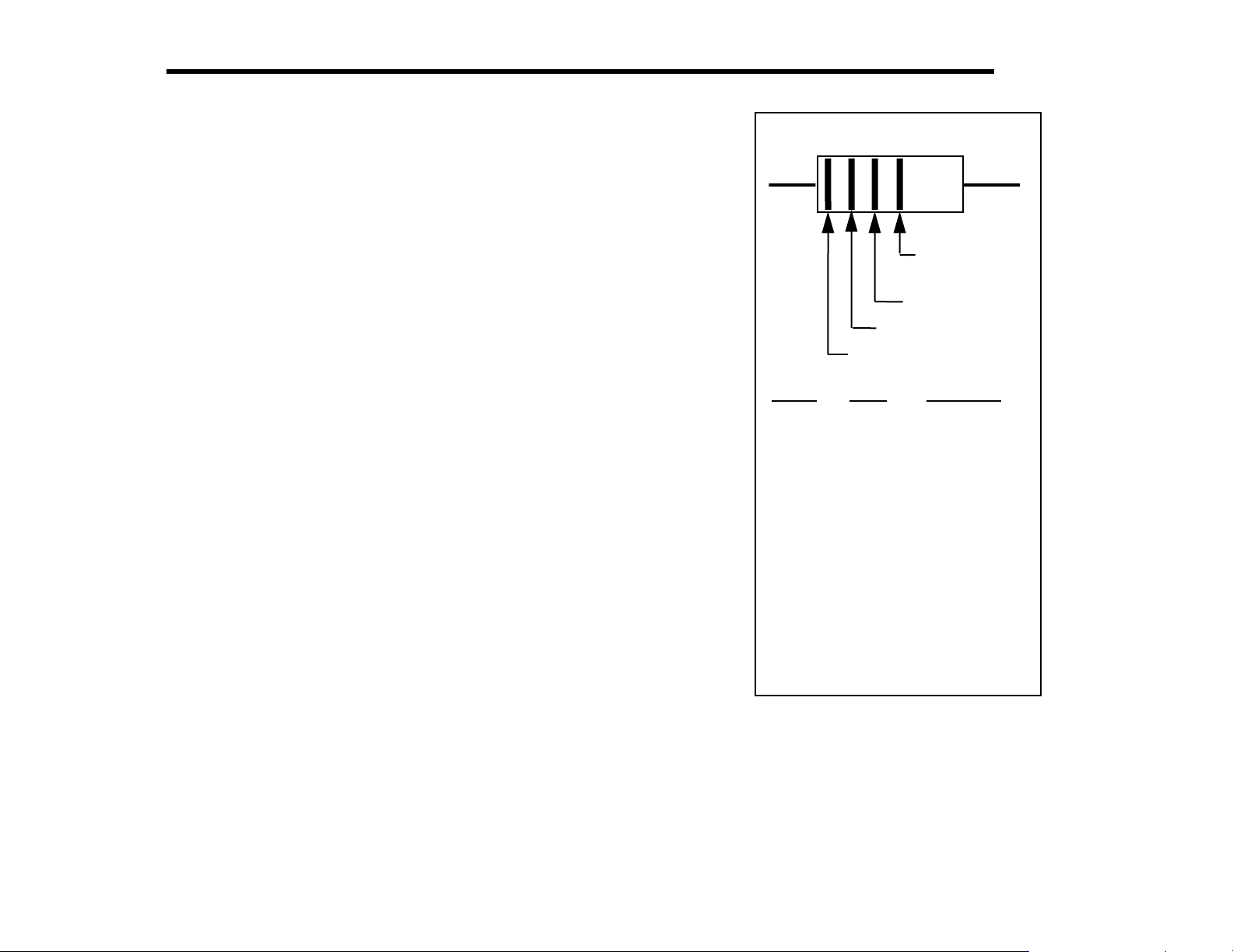
Resistors, Chokes, and the Color Code
All resistor and RF choke color bands are provided in the text along
with their values. However, it is helpful to familiarize yourself with
the color code to allow you to identify these components without
having to refer to the text or parts list each time.
The color-code chart, Figure 3-4, shows how to read the four color
bands on 5% resistors. 1% resistors are similar, except that they use
five bands (three significant digits, multiplier, and tolerance). For
example, a 1,500 ohm (1.5 k) 5% resistor has color bands BROWN,
GREEN, and RED. A 1.5 k, 1% resistor has color bands BROWN,
GREEN, BLACK, BROWN. The multiplier value is 1 rather than 2 in
the 1% case because of the third significant digit.
Because 1% resistors have color bands that are sometimes hard to
distinguish clearly, you should always check their resistance using an
ohmmeter.
The markings on RF chokes reflect their value in microhenries (µH).
Like 5% resistors, chokes use two significant digits and a multiplier.
Example: an RF choke with color bands RED, VIOLET, BLACK
would have a value of 27 µH.
Tools
The following specialized tools are supplied with the K2:
.050" (1.3 mm) Allen Wrench, short handle
5/64" (2 mm) Allen Wrench, long handle
Double-ended plastic inductor alignment tool
Color Code
Tolerance
(gold = 5%,
silver = 10%)
Multiplie
Second Digit
First Digit
Color Multiplie
Black 0 x 1
Brown 1 x 10
Red 2
Orange x 1K
Yellow 4 x 10K
Green 5x 100K
Blue 6x 1M
Violet 7
Gray 8
White 9
Silver -- x .01
Gold -- x 0.1
Digit
x 100
3
Figure 3-4
ELECRAFT
®
11
In addition to the tools supplied, you will need these standard tools:
Fine-tip soldering iron, 20-40 watt (temperature-controlled
preferred, with 700 or 800°F tip [370-430°C]
IC-grade, small-diameter (.031") solder (DO NOT use acid-core
solder, water-soluble flux solder, additional flux, or solvents of
any kind, which will void your warranty)
Desoldering tools (wick, solder-sucker, etc.)
Needle-nose pliers
Small-point diagonal cutters, preferably flush-cutting
Small Phillips screwdriver
Jeweler’s flat-blade screwdriver
While not required, the following items are recommended:
DMM (digital multimeter) for doing resistance and voltage
checks. A DMM with capacitance measurement capability is
strongly recommended (see Identifying Capacitors).
Magnifying glass
Conductive wrist strap
Assembly Notes
i
This symbol is used to alert you to important information
about assembly, alignment, or operation of the K2.
Photographs
You should review the photographs in Appendix D to get an idea of
what the completed PC board assemblies look like.
Step-by-Step Assembly
Each step in the assembly process is accompanied by a check-box:
In some steps you will actually be installing multiple components of a
particular type. In this case the instructions will be followed by a table
listing all of the components to be installed, so you won’t need to refer
to the parts list during assembly. The order that the components are
installed corresponds to their PCB locations.
Do not skip any assembly steps; you may find that you’ve installed
one component that hinders the installation of another.
Forming component leads: In a few cases you’ll find that the space
provided for a component on the PC board is larger than the distance
between the leads on the part itself. In such cases, you’ll need to
carefully bend the leads out and then down to fit the given space.
Always use needle-nose pliers to accomplish this task, and bend the
leads–don’t tug on them. This is especially important with capacitor
leads, which are fragile.
Bottom-Mounted Components
A number of components in the K2 are mounted on the bottom of the
PC boards to improve component spacing or for electrical reasons.
Component outline symbols are provided on both sides of each board,
so it will always be clear which side a particular component goes on.
You’ll be able to tell the top of the board from the bottom easily: the
top side has far more parts. Bottom-mounted parts are identified on the
schematic by this symbol:
Top/bottom interference: In a few cases, top-mounted parts may
interfere with the trimming and soldering of a bottom-mounted part. In
this case, pre-trim the leads of the bottom-mounted part before final
placement, and solder it on the bottom rather than on the top. (Since all
holes are plated-through, you can solder on either side.)

12 ELECRAFT
®
Integrated Circuits and ESD
The K2 transceiver uses integrated circuits and transistors that can be
damaged by electrostatic discharge (ESD). Problems caused by ESD
can often be difficult to troubleshoot because components may only be
degraded, at first, rather than fail completely.
To avoid such problems, simply touch an unpainted, grounded metal
surface before handling any components, and occasionally as you
build. We also recommend that you take the following anti-static
precautions (in order of importance):
Leave ESD-sensitive parts in their anti-static packaging until you
install them
Ground yourself using a wrist strap with a series 1 megohm
resistor (do NOT ground yourself directly, as this poses a shock
hazard)
Make sure your soldering iron has a grounded tip
Use an anti-static mat on your work bench
IC Sockets
Sockets are used for only the largest ICs. You should not use sockets
for the other ICs because they tend to be unreliable and can cause
problems due to added lead length. Since sockets are not used in most
cases, you must double-check the part number and orientation of each
IC before soldering.
Soldering, Desoldering, and Plated-Through Holes
CAUTION: Solder contains lead, and its residue can be toxic.
Always wash your hands after handling solder.
The printed circuit boards used in the K2 have circuitry on both sides
("double-sided"). Boards of this type require plated-through holes to
complete electrical connections between the two sides.
When you solder components on these boards, the solder fills the
plated holes, making excellent contact. This means that you do not
need to leave a large "fillet" or build-up of solder on top of the pads
themselves. A small amount of solder will do for all connections.
Unfortunately, removing components from double-sided PC boards
can be difficult, since you must get all of the solder back out of the
hole before a lead can be removed. To do this, you'll need solder wick
and a vacuum desoldering tool (see techniques below).
The best strategy for avoiding de-soldering is to place all components
properly the first time. Double-check values and orientations, and
avoid damaging parts via ESD.
When removing components:
Don't pull a lead or pin out of a hole unless the solder has been
removed, or you are applying heat. Otherwise, you can literally
pull out the plating on the plated-through hole.
Limit soldering iron contact to a few seconds at a time.
Use small-size solder-wick, about 0.1" or 2.5 mm wide. Use the
wick on both the top and bottom pads when possible. This helps
get all of the solder out of the hole.
Buy and learn how to use a large hand-operated vacuum
desoldering tool, such as the "Soldapullt," model DS017LS. Small
solder suckers are not effective.
With ICs and connectors, clip all of the pins at the body first, then
remove all of the pins slowly, one at a time. You may damage
pads and traces by trying to remove a component intact, possibly
leaving a PC board very difficult to repair.
Invest in a PC board vice with a heavy base if possible. This
makes parts removal easier because it frees up both hands.
If in doubt about a particular repair, ask for advice from Elecraft
or from a someone else with PCB repair experience. Our e-mail
reflector is also an excellent source for help.
ELECRAFT
®
13
4. Control Board
The Control board is the "brain" of the K2. It monitors all signals
during receive and transmit, and handles display and control functions
via the Front Panel board. The microcontroller, analog and digital
control circuits, automatic gain control (AGC), and audio amplifier are
located on this board.
Components
i
Review the precautions described in the previous section
before handling any IC’s or transistors. These components can be
damaged by static discharge, and the resulting problems are often
difficult to troubleshoot.
Open the bag of components labeled CONTROL and sort the
parts into groups (resistors, diodes, capacitors, etc.). If any of the
components are unfamiliar, identify them using the illustrations in the
parts list, Appendix A.
Locate the Control board. It is the smallest of the three K2 PC
boards, labeled "K2 CONTROL" on the front side, in the lower righthand corner. The lower left-hand corner is notched.
Open the bag labeled MISCELLANEOUS and empty the
contents into a shallow box or pan. This will prevent loss of any of the
small hardware while allowing you to locate items as needed.
during manufacturing. Remove the wrenches and wipe off the oil, if
any, then discard the bag.
i
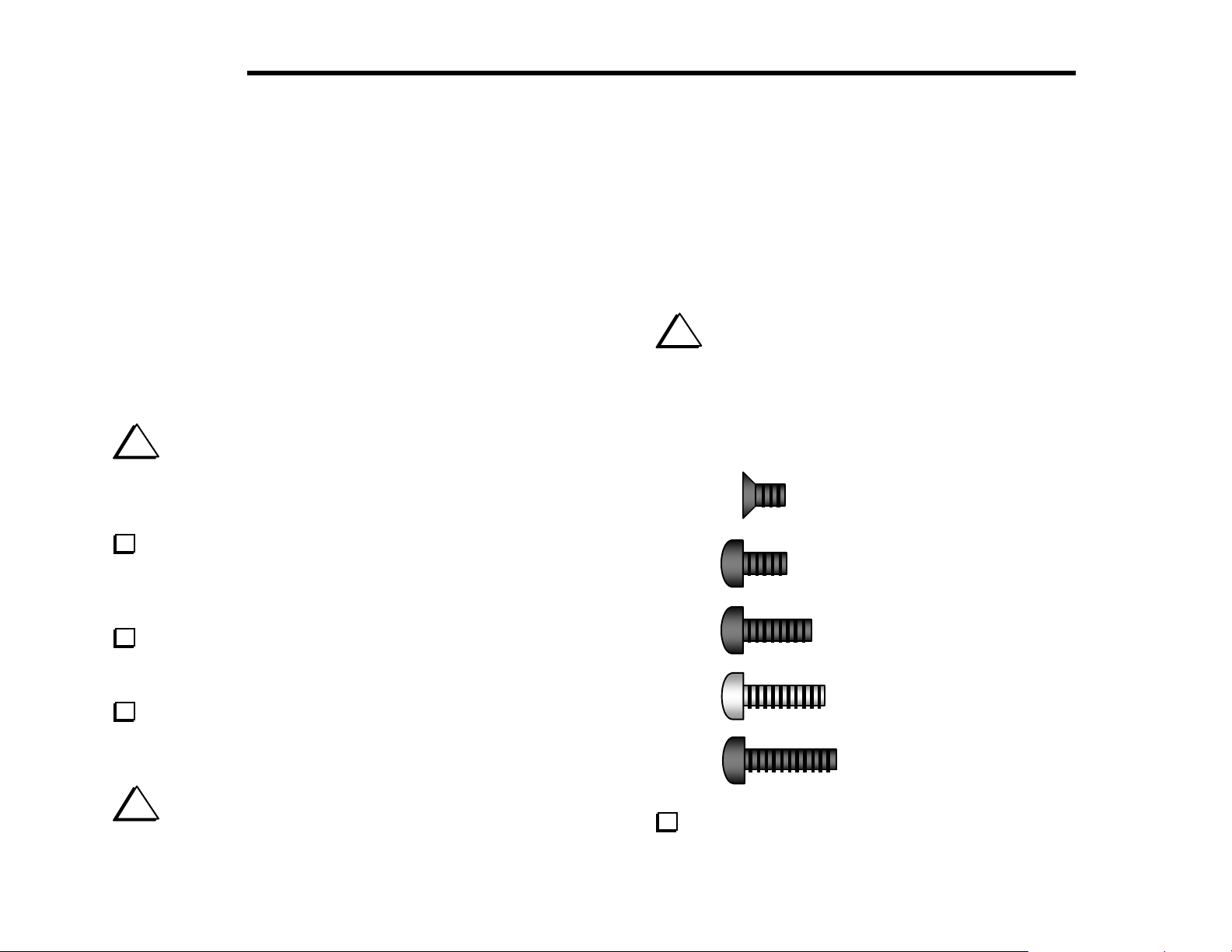
There are five sizes of 4-40 machine screws provided with the
kit. The relative sizes of the screws are shown below for identification
purposes (not to scale). All of the screws are black anodized except for
the 7/16" (11 mm) screws. The 3/16" (4.8 mm) pan-head screws are
the most numerous, and will be referred to as chassis screws
throughout the manual. There is only one flat-head, 3/16" screw.
Flat-head, 3/16” (4.8 mm)
Pan-head, 3/16” (4.8 mm)
(chassis screws)
Pan-head, 3/8” (9.5 mm)
Pan-head, 7/16” (11 mm)
Pan-head, 1/2” (12.7 mm)
i
The Allen wrenches are located in a small bag with the
MISCELLANEOUS items. These wrenches may have been oiled
Identify all of the 4-40 screws and sort them into groups.
14 ELECRAFT
®
Assembly
The side of the Control board with most of the components is the
top side. With the top side of the Control board facing you and the
notch at the lower left, locate the position of resistor R5, near the left
edge. The label "R5" appears just below the resistor’s outline.
Install a 33-k resistor (orange-orange-orange) at R5, with the
orange bands at the top and the gold band (indicating 5% tolerance) at
the bottom. Make sure it is seated flush with the board, then bend the
leads on the bottom to hold it in place. Do not solder this resistor until
the remaining fixed resistors have been installed in the next step.
Install the remaining fixed resistors, which are listed below in
left-to-right PC board order. The resistors should all be oriented with
their first significant-digit band toward the left or top. This will make
the color codes easier to read if you need to re-check the values after
installation. Check 1% resistors with an ohmmeter.
Note: When multiple items appear on one line in a component list
such as the one below, complete all items on one line before moving
on to the next, as indicated by the small arrow. (In other words, install
R5 first, then R2, then go to the second line.)
__ R5, 33 k (ORG-ORG-ORG) __ R2, 3.3 M (ORG-ORG-GRN)
__ R3, 10 k (BRN-BLK-ORG) __ R4, 5.6 k (GRN-BLU-RED)
__ R6, 100 (BRN-BLK-BRN)
__ R7, 1.78 k, 1% (BRN-VIO-GRY-BRN)
__ R8, 100, 1% (BRN-BLK-BLK-BLK)
__ R9, 806 k, 1% (GRY-BLK-BLU-ORG)
__ R10, 196 k, 1% (BRN-WHT-BLU-ORG)
__ R16, 10 (BRN-BLK-BLK) __ R17, 3.3 M (ORG-ORG-GRN)
__ R21, 270 k (RED-VIO-YEL) __ R20, 2.7 ohms (RED-VIO-GLD)
Solder all of the resistors, then trim the leads as close as possible
to the solder joints. Some builders prefer to trim the leads before
soldering. Either method can be used.
Note: Save clipped leads from 1/4-watt resistors that are at least 1/2”
(13 mm) long. You’ll need several of them for ground test points and
other uses later on.
Locate RP6, a 5.1 k, 10-pin resistor network. ("RP" means
"resistor pack," another name for resistor networks.) RP6 is usually
labeled "770103512." Check the parts list for alternative resistor
network labels if necessary. Pin 1 of RP6 is indicated by a dot.
Locate the component outline for RP6 at the left end of the PC
board. Install the resistor network so that the end with the dot is lined
up with the "1" label.
Make sure the resistor network is seated firmly on the board, then
bend the leads at the far ends in opposite directions to hold it in place.
(Do not trim the leads.) Do not solder RP6 yet.
i
Components with many leads are difficult to remove once
soldered. Double-check the part numbers and orientation.
Install the remaining resistor networks in the order listed below.
Do not solder them until the next step.
__ RP1, 3.9 k, 10 pins (770103392) __ RP7, 33 k, 8 pins (8A3.333G)
__ RP2, 82 k, 8 pins (77083823) __ RP3, 47 k, 10 pins (10A3.473G)
__ RP5, 470, 10 pins (10A3.471G) __ RP4, 82 k, 8 pins (77083823)
Solder the resistor networks. (No need to trim the leads.)
Install potentiometer R1 (50 k), located at the left side of the
board. R1 will sit above the board due to the shoulders on its pins.
Hold it in place (flat, not tilted) while soldering.
ELECRAFT
Install the 82 mH shielded inductor (L1) as shown by its
®
15
component outline. Make sure the L1 is pressed down onto the PC
board as far as it can go, then bend the leads slightly to hold it in place
while soldering.
Install the 1N4148 diodes listed below. D1 is in the upper lefthand corner of the PC board. If a diode has only one band, the end
with the band (the cathode) should be oriented toward the banded end
of the corresponding PC board outline. If a diode has multiple bands,
the widest band indicates the cathode end.
__ D1, 1N4148 __ D2, 1N4148
Double-check the orientation of the diodes, then solder.
Find the component outline for diode D3, near the top edge of the
board (right end). Install and solder resistor R22 at this location (82 k,
gray-red-orange).
Install the small fixed capacitors listed below, beginning with C2
in the upper left-hand corner of the board. (This list includes all of the
fixed capacitors on the Control board except the tall, cylindrical
electrolytic types, which will be installed later.) The list shows both
the value and the capacitor labels, using notation explained in the
previous section. After installing each capacitor, bend the leads
outward to hold it in place, but do not solder.
Note: Remember to complete all items in each line before moving on
to the next. (Install C2, C3, and C4, then C7, etc.)
__ C2, .001 (102) __ C3, .01 (103) __ C4, 0.47 (474)
__ C7, 330 (331) __ C6, .047 (473) __ C8, 39 (39)
__ C9, .01 (103) __ C10, .01 (103) __ C12, .0027 (272)
__ C5, .01 (103) __ C14, .047 (473) __ C17, .01 (103)
__ C42, 0.1 (104) __ C16, .047 (473) __ C11, .01 (103)
__ C19, .047 (473) __ C21, 33 (33)
__ C23, .01 (103) __ C20, .001 (102) __ C18, .01 (103)
__ C43, .001 (102) __ C27, .022 (223) __ C25, 0.1 (104)
__ C26, 0.1 (104) __ C24, .0027 (272) __ C31, .01 (103)
__ C34, .001 (102) __ C30, .047 (473) __ C40, .01 (103)
__ C35, .01 (103) __ C36, .0027 (272) __ C39, .01 (103)
__ C41, .01 (103) __ C37, .01 (103) __ C38, 680 (681)
Solder all of the small fixed capacitors.
16 ELECRAFT
®
Install and solder the electrolytic capacitors listed below, which
are polarized. Be sure that the (+) lead is installed in the hole marked
with a "+" symbol. The (+) lead is usually longer than the (–) lead, and
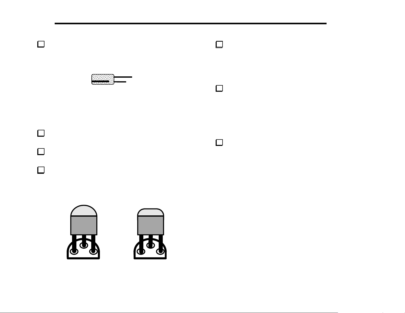
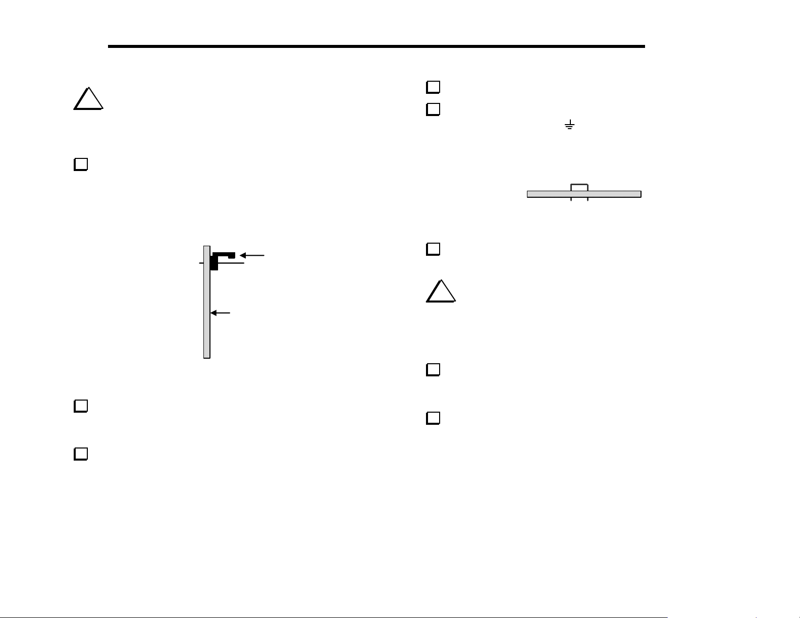
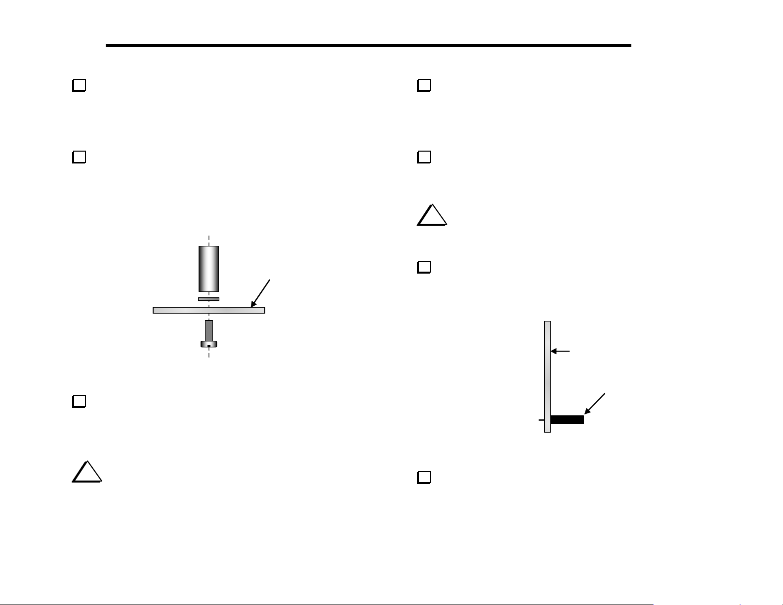
the (–) lead is identified by a black stripe (Figure 4-1).
+
-
Figure 4-1
__ C1, 2.2 µF __ C13, 22 µF __ C15, 100 µF
__ C28, 220 µF __ C29, 220 µF __ C33, 2.2 µF
__ C32, 22 µF
Install and solder ceramic trimmer capacitor C22. Orient the flat
side of this trimmer as shown on its PC board outline.
Using a small flat-blade screwdriver, set C22 so that its
screwdriver slot is parallel to the outline of nearby crystal X2.
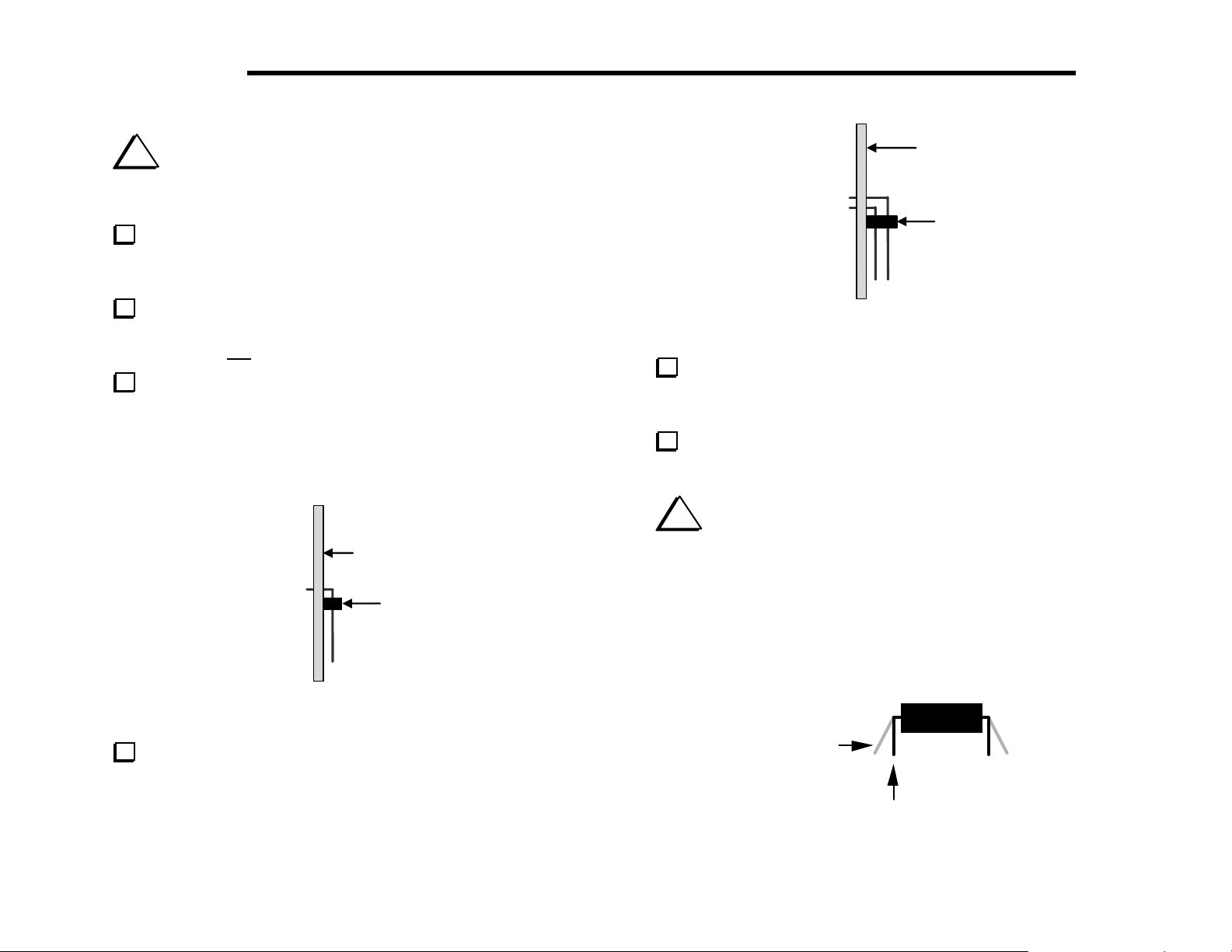
Locate Q12 (type PN2222A), which is a small, black TO-92
package transistor. Q12 and other TO-92 transistors may have either of
the two shapes shown in Figure 4-2. The large flat side of the device
must be aligned with the flat side of the component outline. The
part number may be found on either side.
Install Q12 near the upper left-hand corner of the PC board. Align
the large flat side of Q12 with its PC board outline as in Figure 4-2.
The body of the transistor should be about 1/8" (3 mm) above the
board; don’t force it down too far or you may break the leads. Bend
the leads of the transistor outward slightly on the bottom to hold it in
place. Solder Q12.
Install the remaining TO-92 package transistors in the order listed
below.
__ Q11, PN2222A __ Q1, 2N3906 __ Q2, 2N3906
__ Q3, 2N7000 __ Q4, 2N7000 __ Q5, 2N7000
__ Q6, J310 __ Q7, J310 __ Q8, PN2222A
__ Q9, MPS5179 __ Q10, MPS5179
Solder and trim the leads of these transistors.
Figure 4-2
ELECRAFT
b
Install crystals X1 and X2 so that they are flat against the board.
X1 is 5.068 MHz and is located near the notch in the lower left-hand
corner. X2 is 4.000 MHz, and is located near the center of the board.
Solder the crystals.
®
17
i
The voltage regulators, U4 and U5, will be installed in the
following steps. These regulators have different voltages and must not
be interchanged. Check the labels before soldering.
Prepare two 3/4" (19 mm) jumpers wires from discarded
component leads. These short jumpers will be used to ground the
crystal cans in the next step.
i
Grounding the crystal cans in the following step is required to
ensure proper crystal oscillator performance.
Referring to Figure 4-3, insert the jumper wires into the grounding
holes provided near X1 and X2. Fold each wire over the top of the
crystal and solder it to the top of the can. (Only a small amount of
solder is required.) Then solder and trim the wire on the bottom of the
board.
X1
Figure 4-3
X2
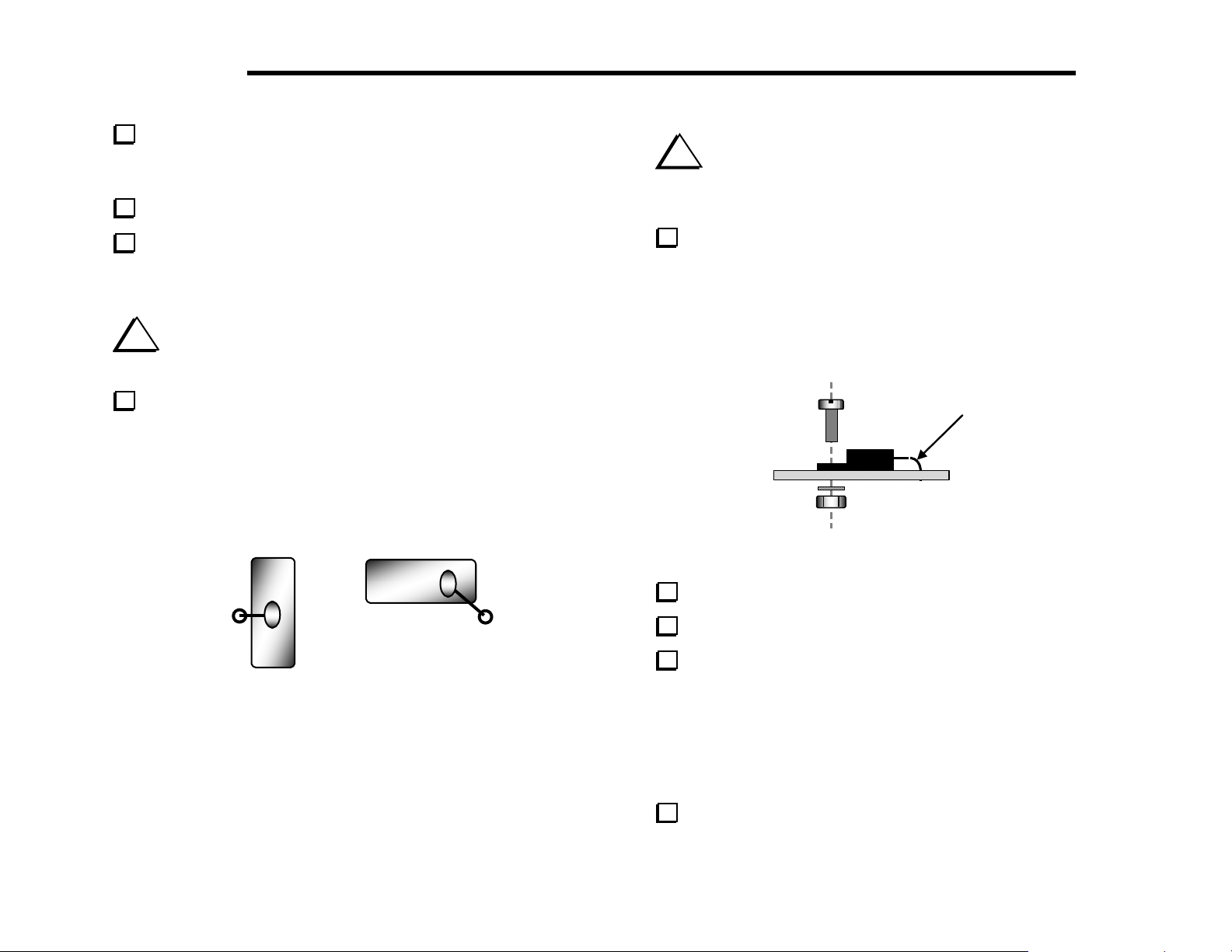
Install U4 (LM2930T-8) and U5 (78M05, 7805T, L7805, etc.),
forming the leads as indicated (Figure 4-4). Fold the pins over the
shaft of a small screwdriver to create smooth bends. After inserting the
leads into the proper holes, secure each IC with a 4-40 x 3/8" (9.5 mm)
machine screw, #4 lock washer, and 4-40 nut. (These regulators may
have either plastic or metal mounting tabs.)
Use smooth
end, not sharp
Figure 4-4
Solder the voltage regulator ICs.
Trim the IC leads as close to the PC board as possible.
Install a 40-pin IC socket at U6. (The microcontroller will be
inserted into the socket in a later step.) Orient the notched end of the
socket to the left as shown on the PC board outline. Bend two of the
socket’s diagonal corner leads slightly to hold the socket in place, then
solder only these two pins. If the socket does not appear to be seated
flat on the PC board, reheat the solder joints one at a time while
pressing on the socket.
Solder the remaining pins of the 40-pin socket.
18 ELECRAFT
Install a shorting jumper onto the two right-hand pins of P7.
i
The connectors used in the following steps have plastic bodies
that can may melt if too much heat is applied during soldering, causing
the pins to be mis-positioned. Limit soldering time for each pin to 3
seconds maximum (1 to 2 seconds should be adequate).
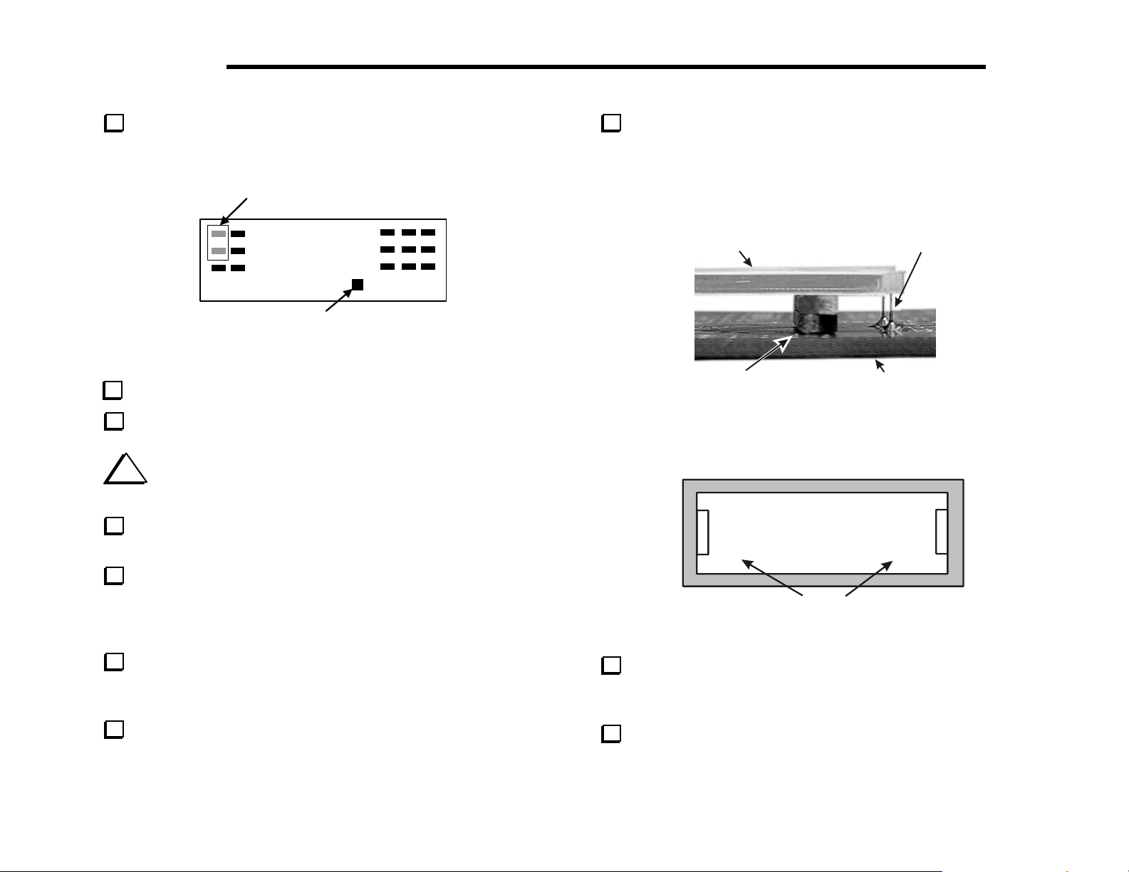
Install the 2-pin male connectors, P5 and P6. As shown in Figure
4-5, the polarizing tab on each connector should be closest to the top
edge of the board. P5, the voltmeter input connector, can be found near
the upper left-hand corner of the board. P6 is used for frequency
counter input, which is in the upper right-hand corner.
Locking
Tab
Top side of
PC Board
Figure 4-5
Install the 10-pin, dual-row connector, P4 (to the left of P5). The
short ends of the 10 pins are inserted into the board. P4 must be seated
flat on the board before soldering.
Install P7, a 3-pin male connector (to the right of P5). The short
ends of the 3 pins are inserted into the board.
At the upper left and right corners of the board are short jumpers,
labeled with ground symbols (
make 3/4" (19 mm) long U-shaped wires for each jumper (Figure 4-6).
Solder the jumpers on the bottom of the board, with the top of the Ushape approx. 1/4" (6 mm) above the board.
Locate the outlines for resistors R18 and R19 on the bottom side
of the Control board.
i
The pads used for R18 and R19 are shared with connectors J1
and J2, which are labeled on the top side of the board. These
connectors are provided with the KAF2 and KDSP2 audio filter
options. You should not install J1 and J2, or an audio filter option,
until after K2 assembly and checkout have been completed.
Install short wire jumpers at R18 and R19. Make the jumpers
from discarded component leads as you did above, but keep them flat
against the board. Solder the jumpers on the top side.
Install the following resistors on the bottom side of the board
(solder on the top side):
__ R12, 820 (GRY-RED-BRN) __ R11, 47 k (YEL-VIO-ORG)
). Use discarded component leads to
Figure 4-6
®
ELECRAFT
i
and P3) will be installed next. It is very difficult to remove them once
they are soldered. Follow all instructions carefully.
Hold the Control board vertically as shown in the side view
below (Figure 4-7). The top side of the board--the side with most of
the components--should be to the right.
Turn to page 8 and review Figure 3-3, which shows how the
Control board plugs into the RF board. P1, P2, and P3 will all be
installed on the top
Position 6-pin right-angle connector P1 as shown in the side view
below (Figure 4-7). Do not solder P1 until the next step. The plastic
part of the connector must be seated flat against the PC board, and the
pins must be parallel to the board. Do not bend or trim the pins on the
bottom of the board.
®
19
The connectors along the bottom edge of the board (P1, P2
side of the Control board as shown.
Top side of
PC Board
P3
Figure 4-8
Install P3, the 20-pin, dual-row right-angle connector (Figure
4-8). Use the same method you used for P1. Do not solder P3 until you
are sure that it is seated properly.
Install P2, the 36-pin, dual-row, right-angle connector. Use the
same method you used for P1 and P3.
i
When you install ICs in the following steps, always straighten
Top side of
PC Board
P1
Figure 4-7
Solder just the two end pins of P1, then examine the placement of
the connector. If P1 is not flat against the board, re-heat the solder on
the end pins one at a time while pressing firmly on the connector.
Once it is in the right position, solder all pins. Do not trim the leads.
the leads of each IC first as shown in Figure 4-9. The two rows of pins
must be straight and parallel to each other to establish the proper pin
spacing for insertion into the PC board or socket.
To straighten the pins, rest one entire row of pins against a hard, flat
surface. Press down gently on the other row of pins and rock the IC
forward to bend the pins into position as shown below.
Flared
Straight
Figure 4-9
20 ELECRAFT
Bend two of U2’s corner pins out slightly on the bottom of the
i
Before handling any IC, touch an unpainted, grounded
metal surface or put on a conductive wrist-strap.
Locate U2, an 8-pin IC, part number LM833. (LM833 is the basic
part number. There may be an additional prefix or suffix or other
markings.) This and all remaining ICs on the Control board are DualInline Packages, or DIPs. Referring to Figure 4-10, identify the
notched or dimpled end of the IC. IC pins are counted starting from
pin 1 (as shown below) and going counter-clockwise.
Notch
board to hold the IC firmly in place, flat against the top of the board.
Find pin 1 and verify that its pad is either round or oval. Once U2 is
properly seated, solder all eight pins, using a minimum of solder.
Install the ICs listed below. Bend the pins to hold each IC in place
as you did with U2, but do not solder until the next step. The notched
or dimpled end of each IC must be aligned with the notched end of its
PC board outline.
Note: For U1, the IC type supplied may be either NE602 or SA602.
__ U1, NE602 __ U3, LM6482 __ U7, 25LC320
__ U8, MAX534 __ U9, LM380 __ U10, LMC660
®
Pin 1
Dimple
Pin 1
Figure 4-10
Straighten the leads of U2 (see Figure 4-9).
Install U2 in the orientation shown by its PC board outline, near
the upper left-hand corner of the PC board, but do not solder it yet.
Make sure the notched or dimpled end is lined up with the notched end
of the PC board outline. Even though the outline is covered when the
IC is installed, you can still verify that the IC is installed correctly by
looking at pin 1. The PC board pad corresponding to pin 1 will be
either oval or round.
i
You may overheat the IC pins or PC pads if you take an
excessive length of time to solder. After a few tries, you should be able
to solder an IC pin in about 1 or 2 seconds.
Check the orientation of pin 1 on each IC by looking at the
associated PC board pads, as before. Then solder all of the ICs.
Locate the microcontroller, U6.
Straighten the pins of U6 (see Figure 4-9). With a large IC such as
this, you can hold the IC body at both ends as you re-form each row of
pins.
i
When the microcontroller is pressed in its socket, you must be
careful to avoid jamming its pins. Make sure that all pins are lined up
with the associated holes in the socket before pressing down on the IC.
Watch the pins on both rows as you press down, re-aligning them with
the socket holes individually if necessary.
Insert the microcontroller, U6, into its socket. Make sure that
pin 1 on the IC itself is lined up with the pin 1 label near the lower
left-hand corner of the PCB outline. Note: The revision label on the
IC (usually white) may not be oriented the same direction as the text
printed on the IC. Do not use the label as a guide--use the notch or
dimple to identify pin 1.
ELECRAFT
®
21
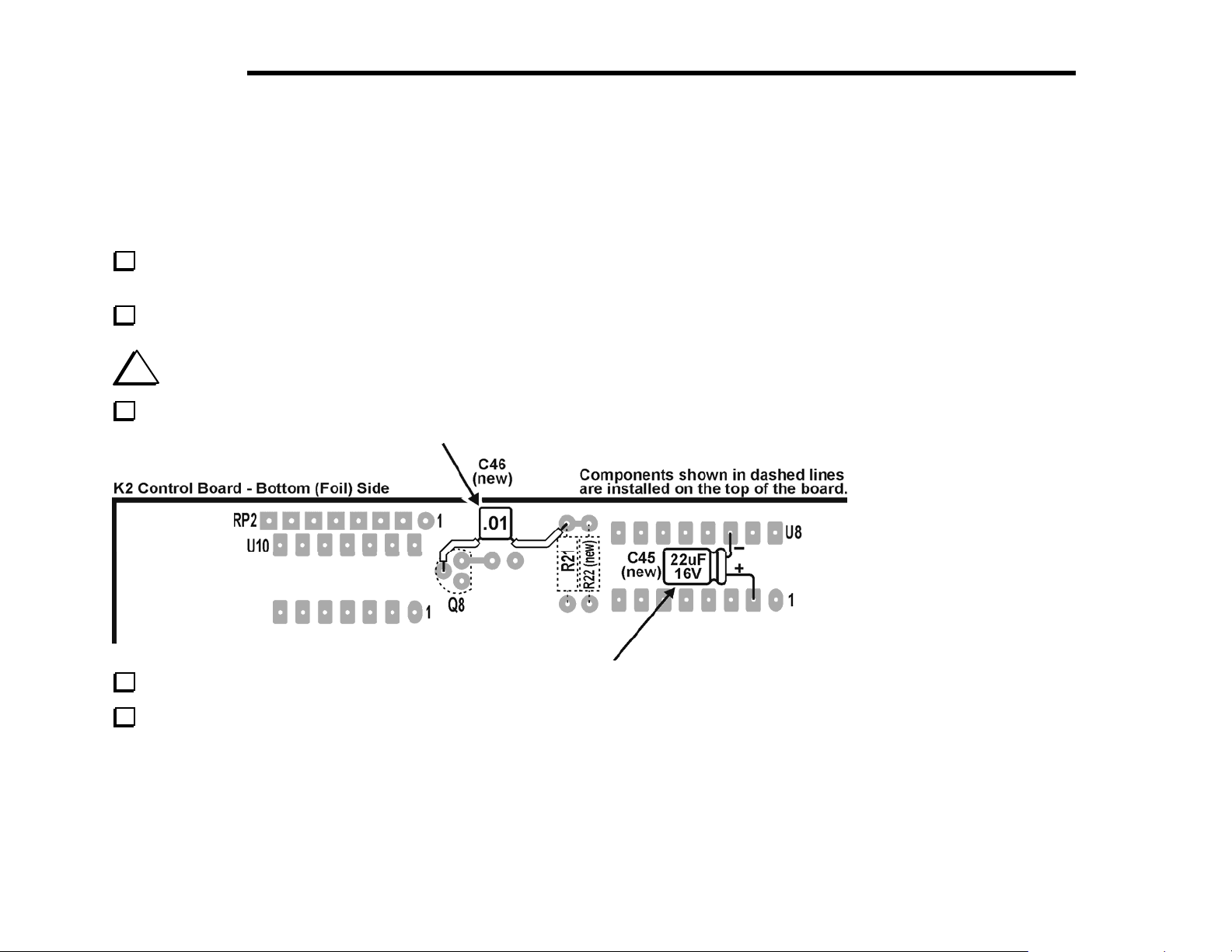
Key Shaping Components (Required)
Your K2 kit includes recent changes that provide an optimized keying envelope shape (sigmoidal, or S-shaped leading and trailing edges).
The result is completely click-free CW transmission. Two of the parts for this change must be installed on the back of the Control board as
described below.
Locate the green insulated hookup wire. Strip two 1/4" (6.4 mm) lengths of insulation from one end of the wire. These will be used to insulate
the leads of C46 in the following steps.
Slip the two lengths of insulation over the leads of a .01 µf capacitor ("103"). This is a new component (C46), not present on the board.
i
Figure 4-11, below, shows the bottom side of the Control board. Components shown with dotted outlines are located on the top side.
On the bottom side of the Control board, solder C46 between R21 and the base lead of Q8 as shown below. Keep lead length short.
Figure 4-11
A 22 µF electrolytic capacitor has also been added (C45). Solder C45 as indicated above, between U8 pin 2 (+ lead) and U8 pin 14 (- lead).
Carefully compare your installation of C46 and C45 to Figure 4-11. Make sure the leads of these capacitors are soldered to the indicated pads.
Verify the orientation of the (+) and (-) leads on C45.
22 ELECRAFT
®
Option Components
All component locations on the Control board should now be filled
except for the following:
C44 (top side of the board near the microcontroller, U6). This
capacitor will not be used.
J1 and J2 (bottom side). These two connectors are provided for an
audio filter option (KAF2 or KDSP2). An audio filter should not
be installed until the K2 has been completed and tested.
Visual Inspection
Nearly all problems with kits are due to incorrectly installed
components or poor solder joints. You can avoid these problems by
doing a simple visual inspection. A few minutes spent here may save
you hours of troubleshooting time.
Make sure there are no components installed backwards. Check
all diodes, resistor networks, electrolytic capacitors, and ICs. (The
parts placement drawings in Appendix F will be helpful when
checking diode orientation.)
Examine the bottom of the PC board carefully for the following
(use a magnifying glass if available):
cold solder joints
solder bridges
unsoldered pins
Resistance Checks
In the table below, "<" means "less than," and ">" means "greater
than." When measuring resistances that show a minimum value in the
table (such as > 100 k), your resistance reading may be much higher or
even infinite. This is typical when using a DMM (digital multimeter).
If you use an analog meter you may find that some or all resistance
measurements are too low. Note: Some digital multimeters will flash
their display to indicate an infinite resistance.
Perform the resistance checks listed below to ensure that there are
no shorts in the most critical control circuits. (The Control board will
be fully tested in a later section.)
Test Point Signal Name Res. (to GND)
P2 pin 1 12V > 10 k
U5, OUT ("5V" pin) 5A > 2 k
U4, OUT ("8V" pin) 8A 3 - 7 k
Q1 collector 8T > 1 M
Q2 collector 8R > 1 M
U3 pin 8 12V IN > 10 k
U6 pin 13 OSC1 > 100 k
U6 pin 14 OSC2 > 100 k
U6 pin 29 DASH 70 - 90 k
U6 pin 30 DOT/PTT 70 - 90 k
U8 pin 2 VPWR > 100 k
U8 pin 15 VBIAS-XFIL > 100 k
U8 pin 16 VBFO > 100 k
ELECRAFT
®
23
5. Front Panel Board
The Front Panel board includes all of the control and display devices
that you’ll use when operating the K2, including the liquid-crystal
display (LCD), LED bargraph, push-button switches, and
potentiometers. See Appendix D for photos of the completed front
panel assembly.
Components
Open the bag labeled FRONT PANEL and sort the parts into
groups (resistors, diodes, capacitors, etc.). Observe anti-static
precautions when handling ICs and transistors.
Locate the front panel PC board, which is just a bit larger than the
Control board. It is labeled "K2 FP" on the top side, in the lower righthand corner.
Assembly
i
Your K2’s appearance and operation will be adversely
affected if the controls or display are not mounted correctly, and in the
indicated sequence. There are also special instructions for installing
components on the bottom of the board.
SWITCH SPACINGTOOL
Figure 5-1
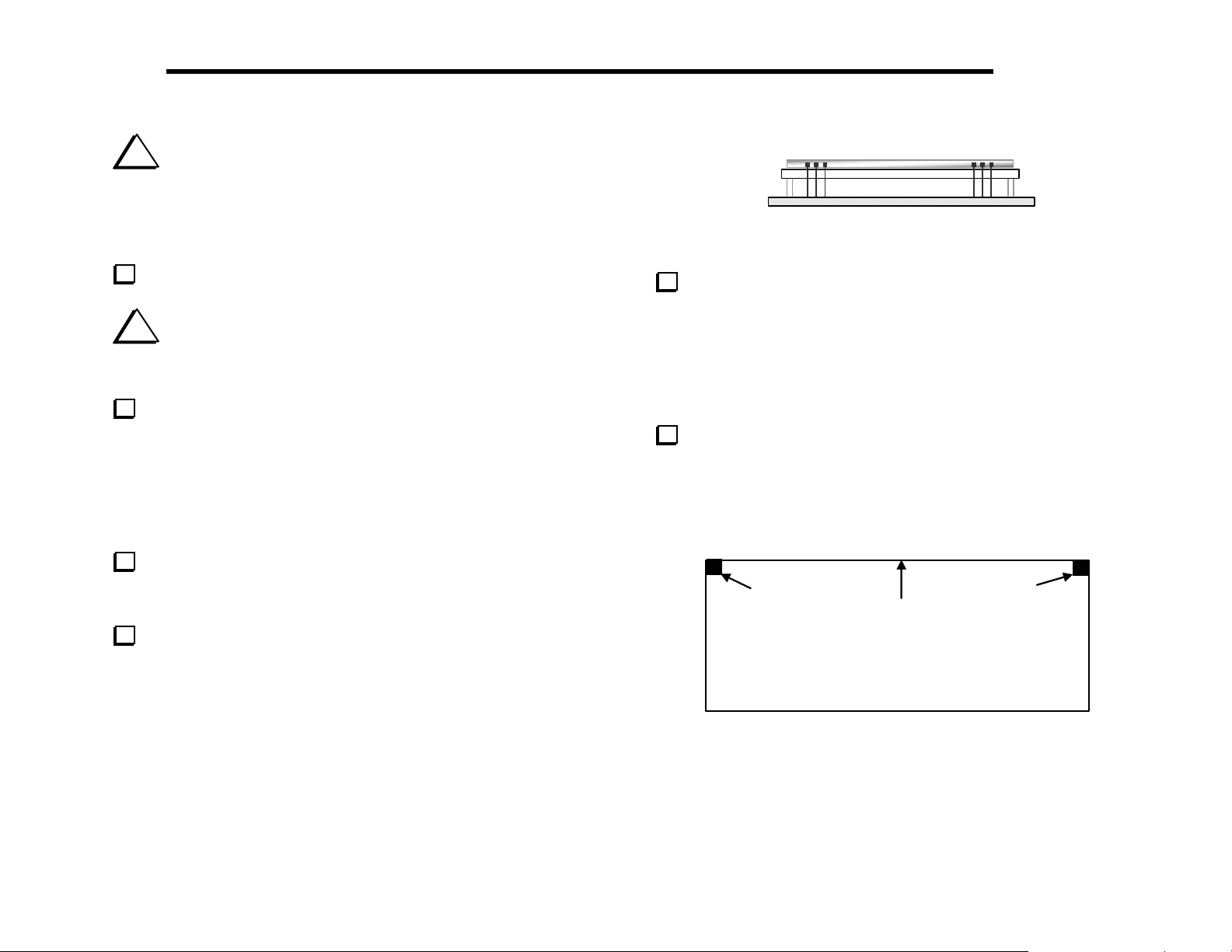
Position pushbutton switches S1 and S2 as shown in Figure 5-2,
using the switch spacing tool to set the switch height. Make sure all
four legs of each switch are centered in their holes, then gently push
each switch until it is resting flush against the switch-spacing tool.
(Caution: switch pins are fragile.) Do not solder yet.
S1 S2
Locate the Spacer Set PC board (Figure 5-1). Using long-nose
pliers, carefully break out the pushbutton switch spacing tool and the
four backlight LED spacers. Break the material only at the four
indicated points. Note: The switch spacing tool doubles as the PC
board for the RF probe, which will be assembled later.
Figure 5-2
24 ELECRAFT
®
Top of
board
1/16”
Figure 5-3
Figure 5-3 shows a side view of a switch that is properly mounted
(spacing tool not shown). The leads of the switches will just be visible
on the bottom of the board. Proper switch height is important for
maintaining an even appearance.
Once you’re satisfied that S1 and S2 are seated correctly, solder
the leads (on the bottom side of the board). Leave the spacing tool in
place until you’ve finished soldering both switches.
Install the remaining switches, S3-S16, using the same technique.
When you get to S8 through S16, you may install three switches at a
time using the spacing tool.
Install the following 1/4-watt fixed resistors, which are listed in
left-to-right PC board order. Solder the resistors after all have been
installed. (R13 and a few other parts are part of the SSB adapter
option, and are not included in the basic K2 kit. A check-list of these
components is provided at the end of this section.)
__ R12, 120 (BRN-RED-BRN) __ R10, 33 (ORG-ORG-BLK)
__ R9, 220 (RED-RED-BRN) __ R11, 470 (YEL-VIO-BRN)
__ R6, 4.7 k (YEL-VIO-RED) __ R7, 4.7 k (YEL-VIO-RED)
__ R14, 100 k (BRN-BLK-YEL)
Install the following resistors on the bottom of the board. Solder
them on the bottom side. Keep your iron tip away from the bodies of
the resistors.
__ R16, 15 k (BRN-GRN-ORG) __ R15, 10 k (BRN-BLK-ORG)
i
When you install the resistor networks in the next step,
you must align the dotted end of the network with the pin 1 label
on the PC board outline.
Install the resistor networks listed below (top side of the board).
Double-check pin 1 orientation and values before soldering.
__ RP2, 120, 10 pins (770101121) (dotted end should be near "RP2" label)
__ RP1, 100 k, 10 pins (10A1.104G) (dotted end near "RP1" label)
Install and solder the diodes listed below, observing proper
orientation as described in the previous section.
__ D4, 1N5817 __ D5, 1N5817 __ D6, 1N5817
Install and solder the following capacitors. C9 is located on the
bottom of the board and must be soldered on the top side.
__ C1, .047 (473) __ C2, .01 (103) __ C3, .047 (473)
__ C9, .01 (103), on bottom
Install PN2222A transistors at Q1 and Q2, near the middle of the
board, and solder. These transistors must be mounted so the lead
length above the PC board is less than 1/8" (3 mm) to prevent them
from hitting the front panel.
There are two ground jumpers on the Front Panel board, one at
the far left and the other at the lower right, labeled with a
Use discarded component leads to make 3/4" (19 mm) long U-shaped
wires for each jumper. Solder them on the bottom side.
Install a 40-pin IC socket at U1, on the bottom of the board. (The
IC will be inserted into this socket later.) Orient the notched end of
the socket to the left as shown on the PC board outline.
symbol.
ELECRAFT
®
25
i
The ICs to be installed in the next step are very sensitive to
static discharge. Touch a grounded surface before handling each
IC. Also note that U4's label will read upside-down (pin 1 at the
right) when properly installed.
Install the following ICs. Before soldering, verify that the ICs are
oriented correctly (pin 1 associated with a round or oval pad).
__ U4, A6B595KA or TPIC6B595
__ U3, A6B595KA or TPIC6B595
__ U2, 74HC165
i
The bargraph LED will be installed in the following two steps.
This component must be seated flat on the PC board or it will interfere
with final front panel assembly. Also, any misalignment will be visible
from the front of the K2.
Locate the bargraph LED, DS2. The bargraph has a beveled
corner or edge that indicates pin 1. Install DS2 as shown by its PC
board outline, just to the left of the LCD. Bend two opposite corner
pins slightly to hold it to the board, then solder only these two pins.
Install the microphone jack (J2) in the lower left-hand corner of
the board, with its polarizing nub at the top (Figure 5-4). Press the jack
down until it is completely flat against the PC board. Re-check the
orientation of the polarizing nub before soldering.
Polarizing
nub
Figure 5-4
Install two 3/16" (4.8 mm) diameter x 1/4" (6.4 mm) long round
standoffs on the top of the board, adjacent to the microphone jack
(Figure 5-5). Use two #4 lock washers between each standoff and the
PC board as shown. Secure the standoffs from the bottom side with
chassis screws. Recall that "chassis screw" is short-hand for 3/16" (4.8
mm) long pan-head machine screws.
If the bargraph is not perfectly flat against the PC board, re-heat
the solder on the corner pins alternately while pressing it down. There
may be small nubs on the back of the bargraph LED. If so do not
remove them. Simply be sure all four nubs are against the PC board.
Once it is in the correct position, solder the remaining pins.
i
Double check to ensure you have soldered ALL the pins on
the LED bargraph. Many builders miss pin 1.
Remove any hardware supplied with the microphone jack, J2. The
nut and washer will not be used.
Figure 5-5
26 ELECRAFT
®
Install another 3/16" (4.8 mm) diameter x 1/4" (6.4 mm) long
round standoff on the top of the PC board, on the left side of the large
square hole in the middle of the board. The standoff mounting hole is
below C2. Use the same hardware as indicated in Figure 5-5, including
two #4 lock washers and one chassis screw.
Install two 1/4" (6.4 mm) diameter x 1/2" (12.7 mm) long hex
standoffs on the bottom of the board (Figure 5-6). The holes for these
standoffs are indicated by large pads on the top and bottom of the
board. Use one lock washer and a chassis screw for each standoff.
Insert the lock washer between the standoff and PC board.
Bottom of
PCB
Figure 5-6
Identify the two different types of panel-mount potentiometers.
Four of them are 5-kohm linear-taper types, labeled "B5K". The fifth
is an audio-taper type, labeled "A5K". They may be physically
identical or have slightly different shafts, body colors, etc.
Install the audio-taper potentiometer, R3, in the lower left-hand
corner. (The PCB is labeled "AUDIO" at R3.) Push only on the
frame, not the shaft. Make sure that the potentiometer body is parallel
to the PC board and is pressed against the board as far as it will go
before soldering.
Install the four 5-k linear-taper potentiometers at R1, R2, R4, and
R5. (The PC board is labeled "LINEAR" at each pot.) Verify correct
positioning as you did in the previous step.
i
Before installing J1 in the following step, review Figure
3-3 (page 8) to be sure you have J1 on the correct side of the
board.
The front panel attaches to the RF board via J1, a 20-pin single-
row female connector. Install J1 on the bottom side of the board
(Figure 5-7). Solder just two pins, one at either end.
Bottom side of
PC Board
J1
Figure 5-7
i
When you install the panel-mount potentiometers in the
next two steps, do not push on the shafts, which may damage the
part. Push only on the metal frame.
Re-heat the two end pins and press the connector down until J1 is
seated flat against the board, then solder the remaining pins.
ELECRAFT
g
®
27
Install rectangular gray key caps on S1 and S3 so the key caps are
parallel to the long axis of the PC board (Figure 5-8). The caps are
installed simply by pressing them onto the switch plungers.
Gray keycaps
Square Keycap
Figure 5-8
Install a square black key cap on S7 as shown above.
Install rectangular black key caps on the remaining switches.
i
Before handling U1, touch an unpainted, grounded metal
surface or put on a conductive wrist-strap.
Straighten the pins of U1, the LCD driver (PCF8566), as you did
with the microcontroller on the Control board.
Position the backlight assembly between the mounting holes
labeled D2 and D3 as shown in Figures 5-9 and 5-10 with two 3/4" (19
mm) long spacers under each end. The diffuser must be parallel to and
1/8" (3 mm) above the PC board. Use a rubber band to hold the
backlight assembly and spacers in place.
diffuser
LED leads
spacers
2 under each end
pc board
(remove after
solderin
LED leads)
Figure 5-9
diffuser
D2
D3
Insert U1 into its socket on the bottom of the board. (This must be
done before continuing with LCD installation, since the LCD’s
presence will make pressing U1 into its socket much more difficult.)
Be sure that U1 is completely seated with no bent pins.
Locate the LCD backlight assembly, which is about 3" (7.5 cm)
long. It includes the diffuser and two small LEDs, one at each end. Do
not remove the backing from either side of the diffuser.
Make sure the LEDs in the LCD backlight assembly are pressed
into the diffuser and are not mis-aligned or loose.
Examine the backlight assembly closely to ensure that it is
parallel to the Front Panel board and seated against the spacers
(exactly 1/8" [3 mm] above the board).
Solder D2 and D3. If the backlight assembly is no longer flat
against the PC board, re-heat the LED pins one at a time and press it
into place.
LED
Figure 5-10
28 ELECRAFT
i
CAUTION: The LCD and its pins are fragile—handle
carefully. Do not drop the LCD on a hard surface, as it is made of
glass and may break. Do not remove the protective plastic film from
the front surface of the LCD until later in this section when the front
panel assembly is completed.
LCD
Figure 5-11
®
Carefully remove the LCD from its packing materials.
i
CAUTION: Do not peel off the thick plastic material on
either side of the LCD, or the LCD will have to be replaced (not
covered under warranty).
Hold the LCD up to a bright light and look at both sides for the
presence of a very thin, clear protective film (like transparent tape). All
LCDs have such film on the front surface of the LCD, which will be
removed in a later step. But the back of some LCDs (not all) may also
have such film, with faintly visible yellow or gray diagonal lines. If
protective film is found on the back side, use a fingernail at one corner
of the LCD to dislodge it, then peel it away.
The LCD has six pins along its lower edge (three on each side),
and 24 pins along the upper edge. Place the LCD in its proper position
on the board but do not solder yet.
The LCD must be seated flat against the diffuser as shown in the
edge view (Figure 5-11). If the LCD does not appear to be seated
correctly, it may be because the backlight LEDs or spacers are misaligned. When the assembly is installed correctly, the LCD’s pins will
all protrude the same distance from the bottom of the board. The leads
may not extend through the solder pad holes.
Solder the four corner pins of the LCD, and then re-check the
alignment of the LCD assembly. If everything looks correct, solder the
remaining pins. LCD pins can be soldered on the top of the board if
they do not protrude from the bottom. If the leads do not reach through
the holes, be sure the solder fills the gap between the lead and solder
pad (see Figure 5-9). After soldering, remove the spacers at each end.
The leads will hold the assembly securely in place.
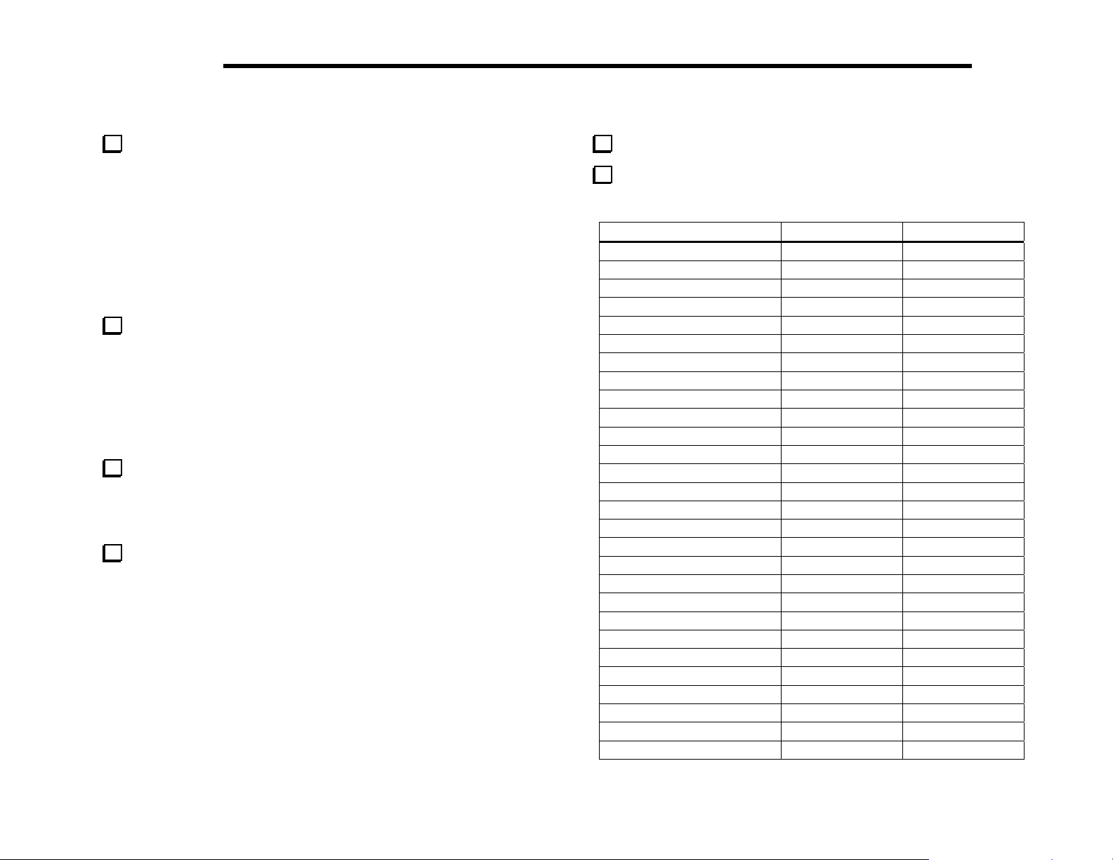
Attach two thin, 1/4" (6.4 mm) self-adhesive rubber pads to the
bottom side of the Front Panel board in the positions indicated in
Figure 5-12. The pads should be placed as close as possible to the
corners, but should not hang over on either edge. These pads establish
the correct spacing for the Front Panel board.
Pad
Pad
Top Edge
(Bottom of PC Board)
Figure 5-12
ELECRAFT
®
29
Uninstalled Components
Check off each of the components in the list below, verifying that
they are not yet installed.
__ C4, .01 (103) __ C5, .01 (103) __ C6, .01 (103)
__ C7, .01 (103) __ C8, .01 (103) __ R13, 68 k, 1%
__ RP3, 10 k resistor network
__ Q3, 2N3906
__ P1 (Mic. Configuration connector, on the bottom of the board)
The unfilled locations (above) are for parts that are provided with
the SSB adapter (model KSB2). If you have the SSB adapter kit, you
should install them now. Follow the third and fourth assembly steps
under Front Panel Board Components in the KSB2 manual (page
16).
Visual Inspection
Make sure there are no components installed backwards. Check
all diodes, resistor networks, electrolytic capacitors, and ICs. The parts
placement drawings in Appendix F will be helpful in verifying the
orientation of diodes.
Examine the bottom of the PC board for solder bridges, cold
solder joints, or unsoldered components.
Resistance Checks
Set all potentiometers to their mid-points (approx.).
Perform the resistance checks (to ground) listed below. U1 is on
the back of the board.
Test Point Signal Name Res. (to GND)
U1 pin 1 IDAT 25 - 35 k
U1 pin 2 ICLK 25 - 35 k
U1 pin 3 /SYNC 40 - 60 k
U1 pin 4 CLK > 50 k
U1 pin 5 5A 15 - 40 k
U1 pin 6 - 11 Ground 0
U1 pin 12 2V 9 - 11 k
U1 pin 13 - 40 LCD segments > 50 k
J1 pin 1 AF gain 1 > 1 M
J1 pin 2 AF gain 2 > 1 M
J1 pin 3 AF gain 3 > 1 M
J1 pin 4 DOT/PTT > 1 M
J1 pin 5 MIC AF > 1 M
J1 pin 6 ENC B > 50 k
J1 pin 7 AUXBUS > 1 M
J1 pin 8 Ground 0
J1 pin 9 SR DOUT > 50 k
J1 pin 10 SR DIN > 50 k
J1 pin 11 SR WRT > 50 k
J1 pin 12 SR CK > 50 k
J1 pin 13 ENC A > 50 k
J1 pin 14 SR RD > 50 k
J1 pin 15 VPOTS 10 - 60 k
J1 pin 16 ICLK 25 - 35 k
J1 pin 17 IDAT 25 - 35 k
J1 pin 18 5A 15 - 40 k
J1 pin 19 RF gain 1.5 - 3.5 k
J1 pin 20 Ground 0
 Loading...