

Page 1

ELECRAFT KPA100 UPGRADE INSTRUCTIONS
Revision A, October 21, 2006
Copyright © 2006, Elecraft; All Rights Reserved
Introduction
The K2/100 transceiver 100-watt final output stage (KPA100 board) has undergone several important changes since it was
introduced. If your KPA100 was built according to any version of the Elecraft manual Appendix G, 100-W Stage and RS-323
I/O (K2/100), up through revision C, this kit will upgrade your older KPA100 board with all the changes to date. KPA100s
built according to revision D or later of the manual already incorporate these changes.
If you have not already done so, you must also install the shield upgrade (order KPA100SHDKT). You can install the shield
upgrade after you have completed the modifications described here.
Tools Required
You will need the following tools to install this modification kit:
Fine-tip temperature-controlled ESD-safe soldering station with 700 to 800F tip (370-430C). Recommend a spade
tip approx. 0.05” (1.3 mm) wide.Do not use a high-wattage iron or soldering gun since this can damage pads, traces,
or the parts themselves.
IC-grade solder, small-diameter (.031”or smaller, Kester #44 or equivalent).
i
DO NOT use acid-core solder, water-soluble flux solder, additional flux or solvents of any kind. Use
of any of these will void your warranty.
A vacuum desoldering tool such as the Soldapullt® model DS017LS. Soldering braid is also handy for removing
excess solder in some situations. See, Soldering and Desoldering below for more information.
#2 Phillips screwdriver with a small handle.
Needle-nose pliers.
Small-point diagonal cutters. Flush-cutting type is required (Xcelite MS54-5J or equivalent).
Digital Multimeter (DMM) for voltage checks and confirming resistor values. A DMM with capacitance
measurement capability is desirable, but not required.
A magnifying glass or visor is often invaluable.
A conductive wrist strap and anti-static mat are strongly recommended. These items are available at very low cost
from Jameco, Mouser, and other electronics suppliers.
Refer to www.elecraft.com for tool sources and solder recommendations.
Soldering and Desoldering
i
Use adequate ventilation when soldering; avoid inhaling smoke or fumes. Always wash your hands after
handling solder, as lead residue is highly toxic.
Removing components from double-sided boards can be difficult, since the holes are plated through to connect with traces on
both sides of the board. A number of suggestions are provided below.
When removing components:
Don't pull a lead or pin out of a hole unless the solder has been removed, or you are applying heat. Otherwise, you can
literally pull the cylindrical plating out of the plated-through hole that joins the top and bottom traces. If you’re having
difficulty, cut the component leads then remove the clipped lead from the hole. Only one component is reused (C83) and
it is clearly identified in the text.
Elecraft • www.elecraft.com • 831-662-8345
Page 2
Limit soldering iron contact to a few seconds at a time.
Use a large vacuum desoldering tool (solder sucker) such as described under Tools Required above. Solder wick is
useful for removing excess solder from a joint, but requires great care if you use it to clean out a hole.
Invest in a PC board vice with a heavy base if possible. This makes parts removal easier because it frees up both hands.
If in doubt about a particular repair, ask for advice from Elecraft or from someone else with PCB repair experience.
Pre-Wound Toroids
Two new toroids are required for this upgrade. They are not difficult to wind, and full instructions are provided. If you prefer
not to wind them yourself, you can obtain a pre-wound toroids from an Elecraft-qualified source. Ordering information can
be found on our web site, www.elecraft.com. You do not need to send your cores or wire to the winding service.
Parts List
We recommend that you do a complete inventory before beginning assembly. The inventory helps you correctly identify all
the parts to avoid mistakes during assembly. The numbers or colors shown in parenthesis are those you should find on each
part. There may be other letters and numbers stamped on the parts as well.
Reference. Designator Description Qty
C64, C79 Capacitor, .0047 µF 5% 250V or greater, LS 0.4 2 E530262
C67, C86 Capacitor, 0047 µF, 100V, LS 0.2 2 E530102
L16, RFC1 Toroid Core, T50-1 (blue) 2 E680001
R4 Resistor, 100k (brn-blk-yel) 1/2W 1 E500006
R19, R20 Resistor, 1.6 ohm (1.6 Ω) 2W 2 E500130
R22 Resistor, 300 ohms (300Ω) 2W 1 E500129
R33 Resistor, 1K (brn-blk-red) 1/2W 1 E500013
R38, R39 Resistor, 22 ohm (22 Ω) 3 W 2 E500128
R40 Resistor, 22k (red-red-org) 1 E500090
RFC4, RFC5 RF Choke, 15 µH (brn-grn-blk) 2 E690006
Misc. #26 Red Enamel Wire 6ft E760002
Misc. #20 Solid Black Insulated Wire 5in E760006
Misc. Thermal pad (for Q1 and Q2) 2 E980051
Misc. Jack screw, Hex, 4-40, M/F 2 E700078
i
The following procedures require you to remove components from the KPA100 printed-circuit board (PCB).
Part
Number
We strongly recommend you use the tools listed under Tools Required and follow the procedures carefully to avoid
damage to the PCB. See the hints under Soldering and Desoldering.
Part I: Removing the KPA100 Board
Disconnect all wires connecting your K2/100 to external devices.
i
Set aside in a safe place all hardware you remove in the following steps for reinstallation later.
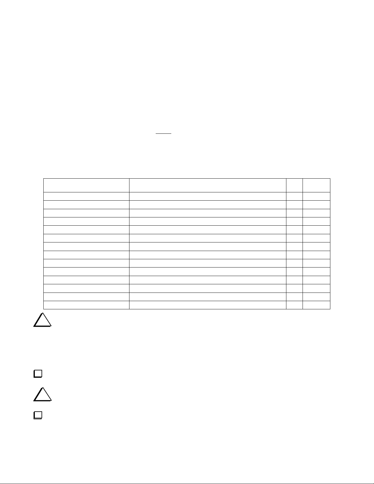
Remove the six screws that attach the KPA100 to the K2: there are two at the top front corners, one on each side of the
K2, and two at the rear.
2
Page 3
Lift the KPA100 up slightly to access the cable connections along the right side. Unplug the ribbon connector that
Standoff
attaches to the control board, the speaker, Aux 12V, and Aux RF connectors that attach to the K2 RF board. Lift the KPA100
off of the K2 and set it top down on a clean surface to avoid scratching the heat sink. Set the K2 aside in a safe place.
Remove the seven screws attaching the shield to the hex standoffs, lift the shield off and set it aside.
If you have the shield modification kit installed, remove the corner screw at J2 holding the solder lugs that connect the
shell of J2 to the hex standoff and shield.
Remove the seven hex standoffs and lock washers that secure the board to the heat sink. Two of the standoffs are near
the center of the board (see Figure 1). Do not lose the lock washers.
1/2 inch
Standoff
Q3
Q4
Q2
Q1
1/2 inch
Figure 1. Removing the KPA100 PCB.
Remove the three screws that attach the KPA100 back panel to the heat sink.
De-solder the two speaker leads at the loudspeaker. Take care not to drop solder on the speaker cone or otherwise
damage it.
Remove the screws securing Q3 and Q4. These screws secure the transistors to the heat sink. Do not lose the lock
washers.
Remove the four screws that secure PA power transistors Q1 and Q2 to the heat sink. Do not lose the lock washers.
Gently lift the KPA100 PCB off of the heat sink. Set the heat sink aside in a safe, clean place. Take care not to damage
the two thermal pads for the transistors. These are small rectangular pads that should remain attached to the heat sink.
Carefully peel the thermal pads off of PA power transistors Q1 and Q2 so that the bottom of each transistor shows clean
metal. You have new thermal pads in the kit to use when reassembling the KPA100. However, the old pads can be reused if
you remove them without tearing or otherwise damaging them.
Remove capacitor C83 from the PCB. Do not damage it. C83 is a large 1000 pF silver mica mounted on the PCB near
the end of binocular core transformer T2. C83 is soldered to the board with two short leads that rest on top of the solder pads
at the end of T2. The leads do not pass through the board. You can remove it easily by removing any excess solder on the
pads, then heating one lead at a time while gently lifting that end of the capacitor. You’ll install it directly on the end of T2
later.
3
Page 4
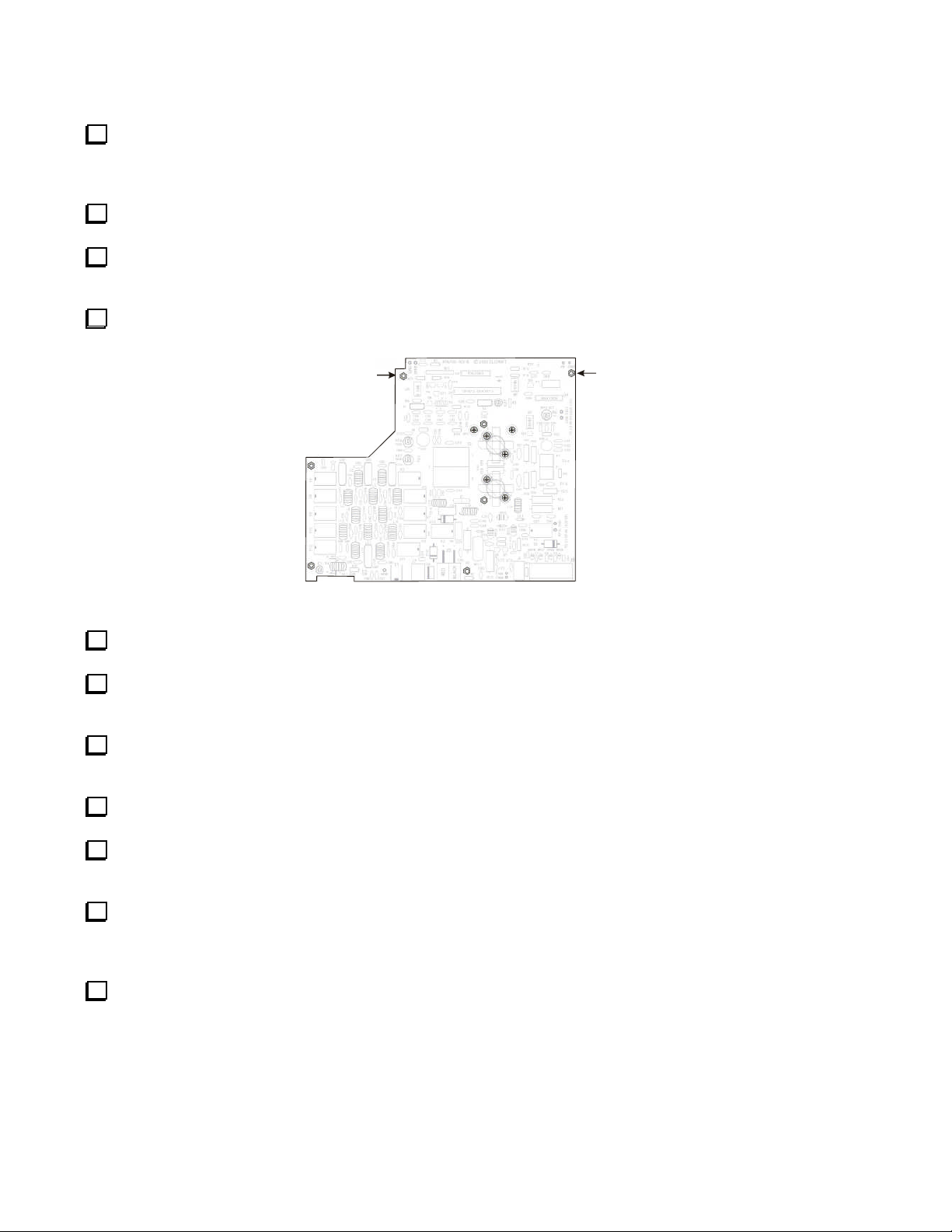
Part II: Input and Feedback Circuit Changes
R19 - 1.6
R20 - 1.6
R23 - Jumper
C82 - Removed
i
Depending upon the age of your KPA100, the following changes to the Input and Feedback circuits may have
already been incorporated. The changed parts and their new values are shown in Figure 2. Proceed directly to Part
III if these changes have been made. Otherwise follow the procedure below to make the changes.
R39 - 22 Ω
R38 - 22 Ω
L18 - Jumper
Figure 2. Input and Feedback Circuit Component Changes.
Remove capacitor C82 (near where the Aux RF coaxial cable attaches to the PCB). C82 will not be replaced.
i
When replacing parts with new parts or jumpers, first remove the old part, then clear the solder pad holes of
all solder before installing the new part. (See Soldering and Desoldering on page 1 for more information.) Install the
new part, solder and trim the leads flush with the PCB.
Replace resistor R23 with a jumper (R23 is near the small binocular core transformers T1.) Make the jumper from a 1”
(25.4 mm) length of the #20 insulated wire. Remove insulation from each end to leave just slightly less than 1/2” (12 mm) of
insulation in the center of the wire. Bend the stripped ends of the wire to fit the solder pads for R23. Solder and trim the
excess leads flush with the PCB.
R22 - 300 Ω
Ω
Ω
Remove insulation from each end, leaving 1/4” (6 mm) of insulation at the center of the wire. Bend the stripped ends of the
wire to fit the solder pads for L18. Solder and trim the excess leads flush with the PCB.
Replace inductor L18 (near Q1) with a jumper. Make the jumper from a 3/4” (19mm) length of the #20 insulated wire.
Replace R22 with a 300 ohm (300 Ω) 2 watt resistor.
Replace R20 with a 1.6 ohm (1.6 Ω) 2 watt resistor..
Replace R19 with a 1.6 ohm (1.6 Ω) 2 watt resistor.
4
Page 5

Replace R38 and R39 with 22 ohm (22 Ω) 3 watt resistors.The replacement resistors are slightly longer than the solder
Form Leads to
Space Resistors
Above the Board.
Position C83
hole pad spacing for them. Bend the leads to space them above the PCB as shown in Figure 3. Position the resistors so they
do not touch each other.
Leave a Small Gap
Between Resistors.
Figure 3. Installing R38 and R39.
Part III: T/R Switch and Output Circuit Changes
Locate C83, the 1000-pF silver mica capacitor that you removed earlier. Bend the leads to the sides where they exit the
body of the capacitor. If necessary, trim them to approximately 1/8" (3 mm) long.
Place C83 in exactly the position shown in Figure 4, extending horizontally away from T2 over R38 and R39. The leads
normally exit the body of the capacitor near the side opposite the markings, so it will be easier to solder if this side is up as
shown. There are no solder pads. The leads lay flat against the tinned end plates on T2. Tin one of the end plates where the
capacitor lead will attach, leaving a small bump of solder on the plate. Then hold the capacitor in place and touch the lead and
plate with your iron to flow the solder onto the lead to hold the capacitor. Solder the other lead, then go back and touch up the
first lead if needed.
higher than the edge of the end plate, the shield may strike the capacitor when it is installed.
i
larger capacitors with 0.4” lead spacing.
larger capacitors with 0.4” lead spacing.
as shown.
See text.
Figure 4. Installing C83.
Check the position of C83 to ensure that no part of the body is higher than the circuit board end plate of T2. If it is
Refer to Figure 5 for the locations of the parts in the following steps.
Replace C86 with a .0047 µF (472), 100V. Use a smaller 0.2” lead spacing capacitor rated at 100 V,not one of the
Replace C67 with a .0047 µF (472), 100V. Use a smaller 0.2” lead spacing capacitor rated at 100 V, not one of the
5
Page 6

C67 - .0047 µF 100V
37T T50-1
Removed
NOTE - If you have a Rev A PCB:
1) L15 has no reference designator
shown on the board.
2) L16 is labeled RFC2.
L15
Removed
C64 - .0047 µF 250V
C79 - .0047 µF 250V
L16
37T T50-1
RFC1
Figure 5. T/R Switch Components.
Replace RFC4 with a 15 µH (brn-grn-blk) RFC.
Replace RFC5 with a 15 µH (brn-grn-blk) RFC .
RFC4 & RFC5
15 µH
C86 - .0047 µF 100V
R12
Remove toroid L15. Nothing replaces it.
Remove capacitor C16 and clear the holes of solder. A new part will be installed here later.
Remove toroid L16 and clear the holes of solder. A new toroid will be installed here later.
Replace C79 with a .0047 µF (472) 250V or greater voltage capacitor, LS 0.4”. The capacitor supplied may be a
different style than that shown in Figure 5.
Remove RFC1 and clear the holes of solder. A new RFC will be installed later.
Prepare a new L16 and RFC11:
1. Use T50-1 cores: blue, 0.5" (12.7 mm).
2. Cut 27" (69 cm) lengths of #26 red enamel wire for each inductor.
3. Wind 37 turns on each core as shown in Figure 6.
1
Pre-wound toroids are available from an Elecraft-approved source; see Pre-Wound Toroids, page 2
6
Page 7

Figure 6. Winding L16 and RFC1.
To Be Removed.
Strip the insulation and tin the leads of both inductors using one of the following techniques:
1. Heat Stripping:
a. Place a small amount of solder (a.k.a. a “blob” of solder) on your soldering iron.
b. Insert the clipped end of the wire into the hot solder. If the iron is hot enough, you should see the insulation
bubble and vaporize after 4 to 6 seconds.
c. Add more solder and feed more wire into the solder as the enamel melts. Continue tinning the wire up to the
edge of the core, and then slowly pull the wire out of the solder.
d. If any enamel remains on the lead, scrape it away using your thumbnail or sharp tool.
2. Burning: The insulation can be burned off by heating it with a butane lighter for a few seconds. Use sandpaper to
remove the residue, then tin the bare wires.
3. Scraping: Use a sharp tool to scrape the insulation away. Work carefully and gently: do not nick the wire. Work
around the entire circumference of the wire to remove all of the enamel and tin the bare wires.
Install the new L16 on the PCB. Be sure you place it in the outline for L16 and not L15. The space for L15 must be
left empty. Solder and trim the leads flush with the PCB.
Install the new C64, a .0047 µF (472) 250V or greater voltage capacitor, LS 0.4”, next to L16. The capacitor supplied
may be a different style than that shown in Figure 5. Solder and trim the leads flush with the PCB.
Remove resistor R12. Nothing replaces it.
Install the new RFC1 on the PCB. Stand the toroid up with the original outline for RFC1 just like the other toroids, even
though the solder pads are spaced much farther apart than is needed.
Remove RFC10, located near the ANT connector (see Figure 7). Clip the leads when removing the choke to avoid
possible damage to toroidal transformer T4 and surrounding components.
RFC10
Figure 7. Location of RFC10.
7
Page 8

Turn the PCB over the and locate the area on the bottom shown in Figure 8.
R33 - 1K
(If Not Installed Elsewhere
Bottom Side
Figure 8. Installing R33 and R40.
of Board
See Text)
R40 - 22K with
Insulated Lead
Strip 1/4” (3mm) of insulation off of the #20 insulated wire, and place the insulation over one lead of 22k (red-red-org)
1/4W resistor R40.
Trim and bend the leads of R40 to just reach the two solder pads shown in Figure 8, with the insulated sleeve protecting
against shorts to the adjacent solder pads. Solder R40 in place as shown, taking care not to cause a solder bridge to the nearby
solder pads.
Check the PCB on both top and bottom to see if R33 has been previously installed. It may be mounted on top of the
board across the leads of RFC3. If R33 is not already installed, position 1k (brn-blk-red) 1/4W resistor R33 as shown and
solder it in place.
Part IV: Other Changes
On the top of the PCB, locate resistor R4 next to crystal X1 and near the edge where the speaker leads are connected.
Check the value of R4. It should be 100k (brn-blk-yel). If it is any value other than 100k, replace it with the 100k (brn-blkyel) 1/4W resistor provided.
Check the hex jack screws on AUX I/O connector J8 on the back panel. If the threaded sections do not reach all the way
through the mounting flanges on J8, replace them with the jack screws provided.
8
Page 9

Reassembly and Test
Locate the thermal pads for Q1 and Q2. You may use the pads you removed if they are not damaged. New pads are
provided with the kit. Remove the small punch-outs at the mounting holes in each pad, if still present in the new pads.
Position the pads on the heat sink with the holes in the pads aligned with the holes in the heat sink. Note that these pads
have no adhesive to hold them in place. Do not omit these pads: the power transistors will be quickly destroyed without
them.
Ensure the bottom of both Q1 and Q2 are clean bare metal with no bits of the thermal pads or other material stuck to
them.
i
Do not use lock washers between the heat sink and the PC board when attaching the board in the next step.
Install the PC board/rear panel assembly onto the heat sink. Press the board down until it is flat against all seven
standoffs on the heat sink, including the two machined standoffs on the pedestal.
Adjust the locations of the thermal pads for Q1 and Q2, if necessary, so that they are still aligned with the mounting
holes. Insert 4-40 x 1/4" (6 mm) pan head screws and split lock washers into the mounting holes for Q1 and Q2 and start the
threads to ensure the thermal pads are held in place. Do not tighten these screws yet. Only screw them in far enough to
engage the threads in the heat sink.
Secure the rear panel to the heat sink using three 4-40 x 3/16" (4.8 mm) black pan head screws.
Tighten the screws to secure Q1 and Q2 to the heat sink Use a small-handled Phillips screw driver to fasten the
hardware tightly without risk of over-tightening or stripping out the screw heads.
Secure Q3 and Q4 to the heat sink using 4-40 x 1/4" (6 mm) pan head screws and split lock washers. Use a small-
handled driver as you did with Q1 and Q2.
Look between the PC board and heat sink to verify that no component leads or bottom-mounted components are
touching the heat sink or associated hardware.
Place a #4 split lock washer over each of the seven set screws.
Install the shorter 1/2" (12.5 mm) standoffs on the two set screws at the front edge of the board. One is near the
"SPKR" and "GND" pads, and the other is near the "AF" and "GND" pads. Do not over tighten.
Replace the remaining 5/8" (16 mm) standoffs on the remaining five set screws.
Re-solder the speaker wires to the loudspeaker terminals. The silver wire connecting to the SPKR pad on the KPA100
goes to the + terminal on the speaker.
9
Page 10

Make the resistance measurements listed below, touching the DMM (+) lead to the indicated points, and the (-) lead to
ground. Note: The reading from J3 to ground may initially read a short (0 ohms) because of the large electrolytic capacitor on
the 12 V line. Use a low resistance range, and wait up to 20 seconds for the reading to stabilize.
KPA100 Test Points (+) Resistance
J3 + lead (red) (see note above) > 5 k
Q1 collector > 10 k
Q2 collector > 10 k
Q1 base 11-16 ohms
Q2 base 11-16 ohms
J2 (antenna jack) center pin > 10 k
Q9 tab (near rear panel) > 10 k
D13 cathode (banded end) > 10 k
Realignment of the KPA100 should not be necessary after making these modifications. If you wish to test or realign the
modified KPA100 before replacing it in your K2, do so now by setting it on books or other support next to the K2 as
described in the KPA100 manual.
Replace the ground lugs, screw and nut removed earlier from one corner of the ANT connector. If your KPA100 does
not have ground lugs attaching the corner of the shield to the ANT connector and the spring clips that ground the shield to the
sides of the K2 case and KPA100 back cover, you must upgrade the shield. Order KPA100SHDKT from Elecraft.
Install the shield on the standoffs with the seven screws you removed earlier, and replace the KPA100 in your K2 by
reversing the steps on page 2.
i
VERY IMPORTANT!
Remember to tighten the mounting screws on Q1 and Q2 after
10 to 12 hours of operation. Failure to do so could destroy the transistors.
Schematic Diagrams
Updated schematic diagrams including the modifications you just made are shown on the following pages.
10
Page 11

W
.Burdic
kE.
Swart
z
Elecraf
t
Rev.Sht.DateB
y
30pF1N57111N57113.3KC1C95C87C88100.001.001200100KR28D16D17R29R27R26T4
432
1
4
3
W
VRFDETC68
1of2LMC6482
U7A
5VC89.01LM358
12CTRL.01
2
1
C100.1R22.7ohms
-BUILDERMUSTCOLOR12VCONNECTORSDIF
FEREN
TLYFROMRFCONNECTORS
AFGNDC110.1R32.7ohm
s1W3W25VQ10Q112N7000SCALE132
3WVREFLVFWDFT50-43FWDREFL
C300.
1
(
0-5V=approx.0-32A
)
E
N
326
+-748
U6R153.3KR1
63.3KC65.01VRFENEL5146C(2beads)GNDSPK
R
RFC11100µ
H*T
50-1L15(notused)T4-
6
T
P
2
H
9/25/06
1
T4-5
LPF OUTLPF IN
C70
(SHEET 2)
C79
250V
.0047
K2
RFC1
15µH
T50-1
12PA
R13
100
R40 22K
R12
(not used)
90-150V
C77
R11
510K
C75
0.1
5T
.015
200V
D14
.01
C73
Q7
ZVN4424
C31
200V
.033
C71
200V
.0018
R33
1K
C64
D13
1N5404
L16
15µH
.001
250V
.0047
C83
R39
22 3W
0.1
C59
4700
C81
R25
C69
.001
U5A
T2
Z = 1:16
4
1
2
s.m.
1000
Q2
2SC2879
10
2W
R34
R35
1.6
2W
R20
RP1
3.9K
1%
8.45K
TP4
1+
-
3
2
5
3
Q1
10
2W
1.6
2W
R19
1
2
RP1
R24
8.45K
7
8
+
5
.047
C57
R38
C58
4700
C80
3.9K
1%
4
U5B
6
.047
.047
C56
C55
22 3W
0.1
.047
.047
470µF
C53
C52
C54 .047
C51
Z1
+
Q4
MJE182
FB110-43
C49
.047
C48
.047
8
-
2
C34
R7 .005 ohms
= on bottom of PC board
Not on the PC board.
1
4
2N3904
+
Q5
3
0.1
I SENSE
R30
3.09k, 1%
231
RFC3
100µH
Q6
ZVN4424
5R
R14
470
12PA
K1
RF IN
2
("AUX RF")
D12
.01
C72
C76
.01
RFC5
15µH
1
GND
RFC4
1N4007 1N4007
D11
C86
15µH
1N4007
.0047
C67
T1
Z = 9:1
5
4
C66
180
R23
0 ohms
(not used)
C82
100V
.0047
(jumper)
10
2W
R21
C63 .047
2W
R22
300
L18
+
7
U7B
LMC6482
-
+
5
R9 10
C62 .047
C61 .047
C60 100µF
0 uH
(jumper)
6
12PA
0.6-0.9 V
D10
R5
15K
R6
1K
5B
Q3
TSENSE
MJE182
1N5404
1
-
+
(Ext. Fuse)
1%
R32
100
0.1
C33
C85
.047
D9
SB530
GND
12K2
2
2
1
-
+
("AUX 12V")
11
Page 12

T2OUT
R2OUT
R1OUT
T1OUT
T3OUT
R3OUT
K2C22.0
1
D1-D8=1N4148Allrela
ysaresh
owninth
eRESET(de-energized)condition
.=onbottomofPCboard(nearesttheh
eatsink).
L13L14C6AC6DC6FC6BC6CC6GL4L5L6C3EC3HC3GC3CC3JC3BC3AL7L8C4DC4EC4CC4BC4AL10L11L12C5DC5FC5EC5CC5GC5BC5
A
K3K5K7K9K11K12K4K6K8K10
L
PFOUTLPFI
N
K
1
L1L2C2DC2EC2CC2BC2A
S.M.S.M.S.M.C3DC3FS
.M.C6
E
TP3
H9/25/0
6
Low-PassFilters
.01
C28
C13-C21
.01
C29
200
R31
FAN-
.01
FAN
S
RP1563.9K
C74
M
FAN+
12CTRL
C90
-5 TO -25V
.01
RS232 Interface
12PA
R1
R8
G
10K
Q9
D
Q12
2N7000
3.3K
RFC6-8: 100 µH
C7-C9, C32: .01 µF
G
IRF830 or IRL620
D
S
U4
MAX1406
1
2
12CTRL
3
4
5
6
7
8
R1IN
R2IN
R3IN
VSS
VCCVDD
T1IN
T2IN
T3IN
GND
C7
C32
RFC8
RFC7
RFC6
TXD
RXD
123456789
RFC9
C9
C8
VRFDET
nc
16
5V
15
14
13
12
11
10
9
/K2 TX
/K2 RX
8R
2
1
4
3
5
6
7
8
9
10
AUXBUS
8T (NC)
12CTRL
VRFDET
AUXBUS
C84
.001
15µH
C97
J8
.01
(BACK VIEW)
12CTRL
C99
.01
C98
1 2 3 4 5
.01
6 7 8 9
2
/OUT1
IN1
3
1413121110
15
/OUT2
/OUT3
IN2
IN3
5
4
1/2W
/OUT4
IN4
COM
/OUT5
/OUT7
/OUT6
IN5
GND
IN7
IN6
987
6
181716
/OUT0
U2
TD62083
IN0
or ULN2803
1
5B
nc
SCALE
VRFEN
TP1
BIAS SET TEST POINT
12PA SENSE
C27
30pF
12
 Loading...