Page 1

KPA100 UPGRADE INSTRUCTIONS
Rev. B, Feb. 24, 2004
Introduction
The following changes raise the SWR threshold that can be accommodated by the KPA100 before it does automatic
power reduction. Once the changes have been made, KPA100 firmware revision 1.08 or higher can optionally be used
(order #FWKPA100), which starts power reduction at an SWR of 2:1 rather than 1.5:1.
The modification kit also includes an 18.432 MHz replacement crystal for use at X1. A new frequency was chosen to
improve rejection of spurious products, although the KPA100 was in compliance at the original frequency.
Finally, the kit provides two solder lugs. These are used to fashion a jumper that provides a better ground-return path
from the PA shield to the KPA100's antenna jack. NOTE: We also recommend installing the upgraded KPA100
shield (order #KPA100SHLDKT) if you have not already done so. In addition to a replacement shield, the kit includes
three ground clips that keep the shield in contact the K2 side panels and the rear panel of the KPA100.
Modification Procedure
Turn off the K2, turn off the power supply, and disconnect all rear-panel cables.
Remove the six screws retaining the KPA100 module and lift it out carefully, disconnecting all cables.
Remove the seven zinc-plated (bright) screws holding the KPA100 shield to the PC board. Do not remove the
three black screws that hold the grounding clips to the shield (applies if you have the newer shield).
Remove the KPA100 PC board from the heatsink as follows: (1) remove the seven shield standoffs; (2) remove the
six screws holding transistors Q1-Q4 to the heat sink; (3) remove the three screws holding the rear panel to the
heatsink; (4) desolder the speaker wires at the speaker; (5) lift the board off the heat sink.
Remove crystal X1 (16.289 MHz) and replace it with the new crystal supplied (18.432 MHz).
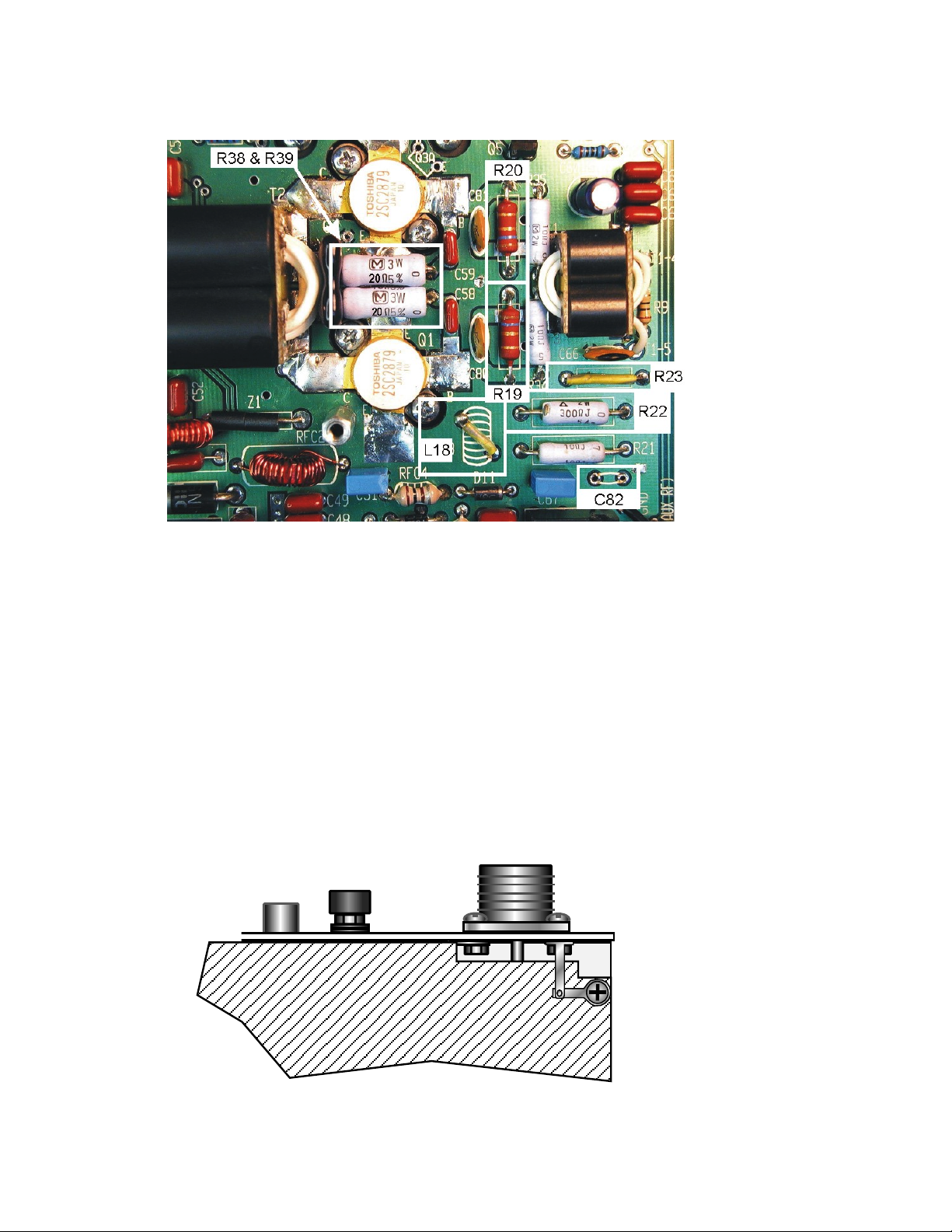
Refer to the Figure 1 (on the back of this sheet) during the remaining steps.
Desolder and remove C82. It will not be replaced.
Desolder and remove R19 and R20, being very careful not to damage the pads. Clean the holes out using solder
wick or a vacuum desoldering tool.
Replace R19 and R20 with 1.6-ohm, 2-watt resistors. Save trimmed leads for use as jumpers in later steps.
Desolder and remove L18.
Replace L18 with a short wire jumper just long enough to span the two pads and sit about 1/8" (3 mm) above the
board. Make the jumper from a component lead or hookup wire. It should not touch adjacent pads or components.
Desolder and remove R22. Replace R22 with a 300-ohm, 2-watt resistor.
Desolder and remove R23. Replace R23 with a short wire jumper made from a discarded power resistor lead
between the existing leads. Make sure the new jumper is not touching any adjacent pads, components, or traces.
Look closely at the leads of R38 and R39 that are closest to silver-mica capacitor C83. If C83 is positioned so that
it will be difficult to get at the leads of the two resistors, temporarily remove it. You should first remove the two
standoffs to the left and right of Q1 & Q2, to permit unobstructed access to the solder pads of all three components.
Remove R38 and R39.
Replace R38 and R39 with 22-ohm, 3-W resistors. The new resistors are larger than the originals, so you'll need to
leave the leads somewhat longer and form them to fit the pad spacing. Space the resistors about 1/16" (1.6 mm) above
the PC board, and about the same distance apart. (NOTE: The photo shows 20-ohm resistors rather than 22 ohm.)
If you removed C83, replace it now.
Examine the thermal pads for transistors Q1 and Q2. You will not need to replace the thermal pads as long as all of
the material is still in place. Some of the pad material may be sticking to the flanges of the transistors rather than to the
heat sink, which will not impact thermal performance. But if any of the pad material has fallen off, replace both of the
pads (see the KPA100 manual, Figure 35). Replacement pads are order #KPA100TH.
1
Page 2

Reinstall the PC board and standoffs. Follow the instructions on page 40 of the KPA100 manual to be certain you
reinstall the hardware correctly. The instructions regarding Q1-Q2 hardware are especially important.
If you've purchased a KPA100 firmware upgrade, install the new IC at U1 now (16F872).
Figure 1
If you've purchased a KPA100 shield kit, assemble and install the new shield now using the supplied instructions.
Otherwise, reinstall the original shield. Note: Your KPA100 shield upgrade kit may have included fabrication of the
solder lug ground strap. In that case, skip the next four steps.
The solder lugs will be used to form a ground strap between the shield and rear panel as shown in Figure 2. Attach
one lug to the shield screw near the SO239 connector. The lug replaces the original lock washer.
Attach the second lug to the upper-right of the four screws holding the SO239 connector to the rear panel. This lug
also replaces the original lock washer.
Using long-nose pliers, fold the second lug down at a 90-degree angle so that it overlays the first as shown below.
Trim the excess length off the end of the first lug. Solder the two lugs together.
Tighten the hardware to ensure good contact at both ends of the ground strap.
Turn the KPA100 assembly over carefully and install it in the K2, re-connecting all internal cables. Make sure the
left and right spring clips are touching the side panels, and that none of the interconnecting cables are pinched.
Turn the K2 on. Follow the Temperature Calibration (CAL tPA) steps on page 45 of the KPA100 manual.
J2
Figure 2
J7
E1
2
 Loading...