

Page 1

ELECRAFT KDSP2
INTERNAL DSP FILTER and REAL-TIME CLOCK
Assembly and Operating Instructions
Revision A.1, June, 2003. Copyright © 2003, Elecraft; All Rights Reserved
Introduction
The KDSP2 DSP Filter is designed specifically for internal operation with an Elecraft K2 transceiver.
For the CW operator
The KDSP2 provides filter bandwidths from 50 to 800 Hz, with center frequencies from 400 Hz to 1,300
Hz, to help eliminate nearby interfering signals. The filters may be easily adjusted from the front panel,
and up to four (4) filters may be selected by the AFIL button.
Noise reduction helps reduce QRN, and may be used with any of the CW filters.
For the SSB operator
A tunable bandpass filter is settable from the front panel, offering low-frequency cutoff (high pass filter
function) from a few tens of Hz to 600 Hz, and a high frequency cutoff (low pass filter function) from 1.6
kHz to 3.0 kHz.
In addition to the tunable bandpass filter, an automatic notch filter quickly locates and suppresses
interfering carriers, such as those caused by other stations tuning up nearby. Noise reduction is also
available and may be used in conjunction with the bandpass and autonotch filters.
For the Data operator
Bandpass filters tuned for common HF data modes, such as RTTY, Packet and PSK31 are provided.
Center frequencies vary from 1 to 2.5 kHz, and widths from 50 Hz to 1 kHz.
Noise reduction and notch filters are not available in data modes as phase distortion may result in poor
copy on an otherwise clean-sounding signal.
Convenience Features
All filters are adjustable from the front panel. Up to four (4) filters per mode (CW/SSB/DATA) may be
memorized. The filters are then selected by simply pressing the AFIL button. A front-panel selectable
bypass mode is available which significantly reduces current consumption.
Elecraft • www.elecraft.com • 831-662-8345
Page 2

Real-Time Clock
The real-time clock displays 24-hour time, as well as date. You’ll find the clock convenient for field
operation. Time can be easily set from the front panel of the K2. The on-board lithium cell will power the
clock for several years.
.
Flash-based Software
The KDSP2 functions are fully defined in software. The DSPx Module is Flash-based. The
microcontroller on the interface card is also Flash-based.
Specifications
Band-pass filters Flatness: better than 1 dB, Attenuation: better than –50 dB
Center frequency adjustable 400 Hz to 1 kHz in 50 Hz steps,
and from 1 kHz to 2500 Hz in 100 Hz steps, mode dependent .
Width adjustable 50 Hz to 3 kHz in 50 Hz or 100 Hz steps, mode dependent.
Normal and “soft” filters available in CW mode.
Automatic Notch Adaptive, with coefficient adjustment by operator.
Noise Reduction Adaptive, with level and coefficient adjustment by operator
Clock Accuracy +/- 20 ppm (+/- 1.7 seconds per day) at 25 degrees C
Date Formats MM-DD-YY or DD-MM-YY; handles all calendar months and leap years
Current Drain Approximately 60 mA active, 10 mA standby
Size 3.12" (L) x 1.2" (D) x 2.1" (H) (8.1 x 3.1 x 5.2 cm)
i
NOTE: Some parts in this kit can be damaged by static discharge. Before handling any
transistors or ICs, put on an anti-static wrist strap, or touch a grounded, unpainted metal surface.
Firmware Requirements
The main microcontroller firmware in the K2 must be version 2.01 or later. If you have an earlier version,
contact Elecraft for an update. You can install the firmware upgrade during assembly of the KDSP2, but
we recommend you install it ahead of time and verify correct operation of your K2 before you build and
install the KDSP2.
The firmware resides in the main microcontroller (U6) of the K2, on the K2 Control Board. You may
check the firmware revision by holding any button when powering up your K2. When you release the
button, the firmware revision will be briefly shown on the left side of the display.
2
Page 3
Assembly
Parts Inventory
Please check the enclosed parts with this list. Check off each item in the space provided. The number
following the check-off space is the quantity required. The part numbers referenced are not necessarily
marked on the parts. Rather, they are provided for reference when ordering replacement parts.
Parts Sorting
As you sort the parts, you may find it convenient to place them in a compartmented container for ready
access. Be careful of static electricity issues if you use an insulated container to hold the parts. Use of tape
to hold sorted parts is discouraged, as there is danger of static buildup as well as contamination of the leads
from adhesive residue.
i
NOTE: do not put ICs or any semiconductor component in a Styrofoam or other plastic container,
or damage from static may occur. Leave such parts in the envelope or foam provided until they
are called out in the assembly instructions.
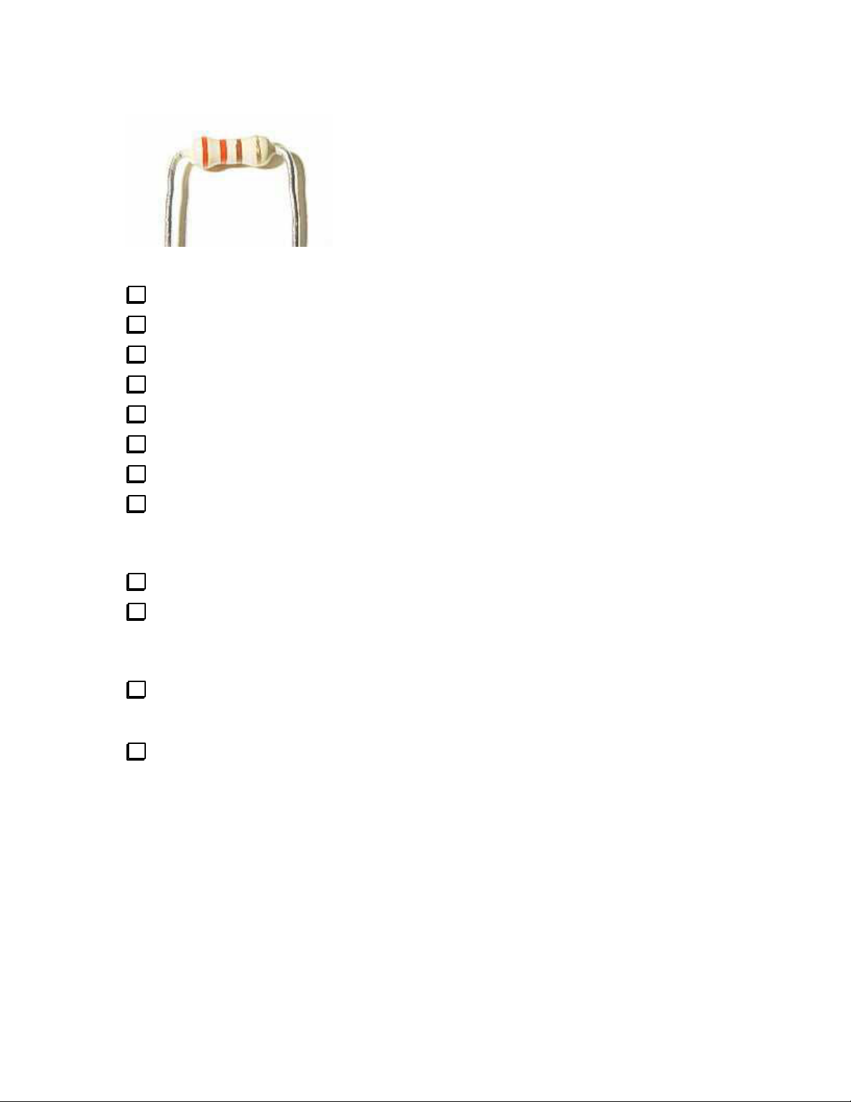
Resistors
¼ watt, 5%, carbon film
OK Qty Reference Value Color Code Part Number
3 R6-8 120 ohm brown-red-brown-gold E500022
2 R11, R13 220 ohm red-red-brown-gold E500002
2 R17, R18 470 ohm yellow-violet-brown-gold E500003
2 R15, R16 2.2K red-red-red-gold E500107
7 R1-5, R10, R19 10K brown-black-orange-gold E500015
1 R9 47K yellow-violet -orange-gold E500067
1 R14 1M brown-black-green-gold E500024
2 watt, 5%, metal oxide
OK Qty Reference Value Marking Part Number
1 R12 43 ohm 430J or yellow-orange-black-gold E500108
3
Page 4
Capacitors
OK Qty Reference Value Type Marking Part Number
1 C6 33 pF Ceramic Monolithic 33 or 330 E530144
1 C12 470 pF Ceramic Monolithic 471 E530080
3 C7, C9, C13 0.01 uF Ceramic Monolithic 103 E530019
4 C3,-5, C8 0.1 uF Ceramic Monolithic 104 E530020
2 C11, C15 0.33 uF Film 330n or 334 E530145
2 C10, C14 10 uF Electrolytic, low profile 10 uF E530045
2 C1, C16 10 uF Electrolytic 10 uF E530142
1 C2 22 uF Electrolytic 22 uF E530143
Connectors
OK Qty Reference Value Description Part Number
1 P2 3-pin Male Header, 1x3, 0.025” square post E620053
1 P1 5-pin Male Header, 1x5, 0.025” square post E620052
1 Ctrl-J2 3-pin Female Header, 1x3 E620009
1 Ctrl-J1 5-pin Female Header, 1x5 E620051
1 J2 12-pin Female Header, 1x12 E620008
1 J1 20-pin Female Header, 2x10 E620038
1 28-pin IC Socket, 0.300” wide E620011
1 3-pin Lithium Cell Holder E980040
Transistors
OK Qty Reference Value Marking Part Number
4 Q1, Q3-4, Q7 2N3904 2222, 3904 E580017
1 Q2 2N3906 2907, 3906 E580000
2 Q5-6 J309 J309 E580009
Diodes
OK Qty Reference Value Marking Part Number
1 LED1 LED, Red None E570012
4 D1-4 1N5711 or SD101A 1N5711, SD101A E560004
2 D5-6 1N4148 1N4148 E560002
4
Page 5
Integrated Circuits
OK Qty Reference Value Marking Part Number
1 U1 ATmega8L ATMEGA8L E610015
1 U2 LM340T-5.0 LM340, 7805 E600024
1 U3 NJU6355ED NJU6355 E600038
Note that U3 is pre-programmed with the KDSP2 application code.
Hardware
OK Qty Description Part Number
1 4-40x1/4” Philips pan head screw E700005
1 4-40x0.5” Aluminum hex male-female threaded spacer E700057
Miscellaneous
OK Qty Reference Value Description Part Number
1 Y1 32.768 kHz Crystal, Cylindrical E660015
1 Z1 4 MHz Ceramic Resonator, 3-pin E660001
1 BT1 3V CR-2032 Lithium Cell E980039
1 DSPx Assembled DSP Module DSPX
1 DSP2 Printed Circuit Board E100179
1 KDSP2 Instruction Manual E740050
1 1/2 x 3/8 x 2 Gray Foam E980070
1 3/8 x3/16 x 2 Black Foam E980069
Installing Components
Please install the parts in the order shown. After you mount a part, you may solder it in place. Double
check to be sure the part is snug against the printed circuit board (PCB). After soldering, clip the leads
close to the PCB surface.
Use a temperature-controlled soldering iron, set between 700 and 735 degrees F (370 to 390 C). Keep the
tip clean. Use rosin-core solder. Use of improper flux, or improper cleaning procedures may result in
corrosion of the soldered joint. Sometimes this takes days or weeks to appear.
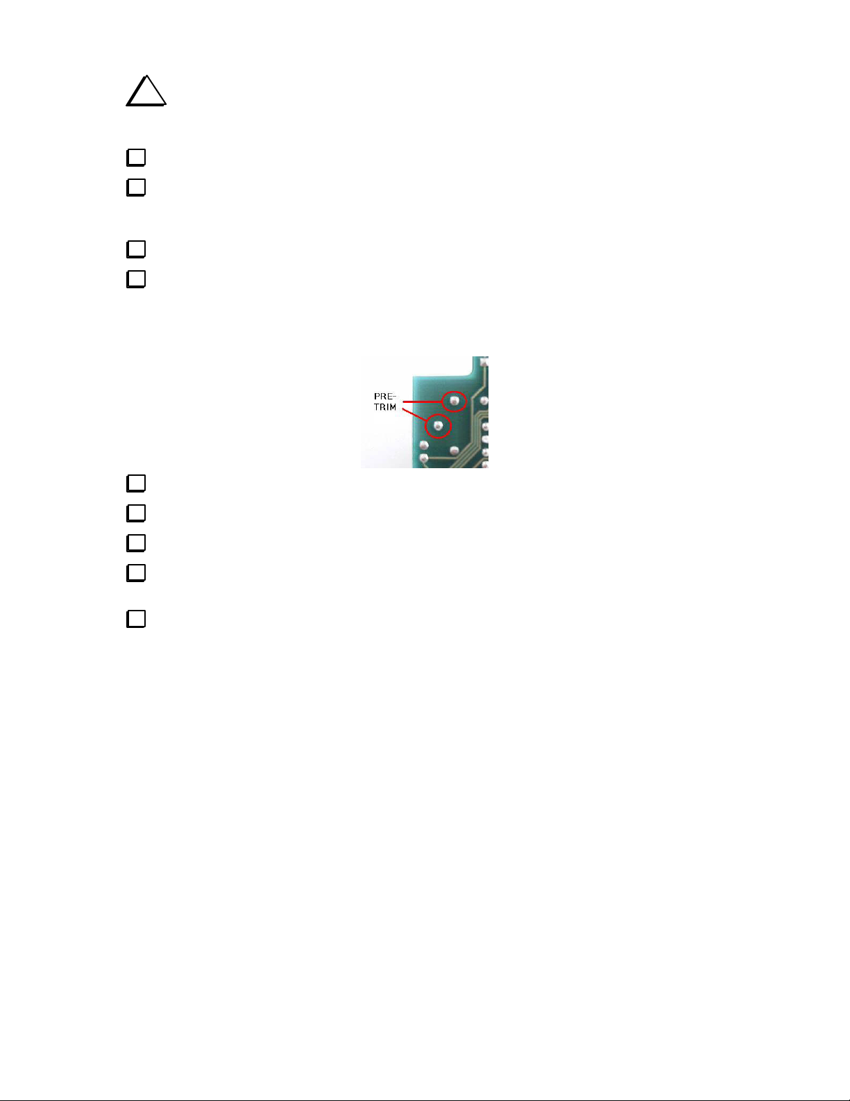
i
It is important that leads be clipped close to the bottom of the PCB. Use a pair of flush-
cutting pliers, or pre-trim the leads before soldering.
As you install the following parts, check the box only after you have inspected the solder connection and
clipped the leads (unless directed to not clip the leads).
5
Page 6
You should pre-bend the leads of resistors close to the body and at right angles. Quarter-watt resistor
locations on the PCB have 0.35” centers (9mm).
Near the upper left hand corner of the PCB:
R1 10K ohm ¼ watt 5% carbon film resistor (brown-black-orange-gold)
R2 10K ohm ¼ watt 5% carbon film resistor (brown-black-orange-gold)
R3 10K ohm ¼ watt 5% carbon film resistor (brown-black-orange-gold)
R4 10K ohm ¼ watt 5% carbon film resistor (brown-black-orange-gold)
R5 10K ohm ¼ watt 5% carbon film resistor (brown-black-orange-gold)
R6 120 ohm ¼ watt 5% carbon film resistor (brown-red-brown-gold)
R7 120 ohm ¼ watt 5% carbon film resistor (brown-red-brown-gold)
R8 120 ohm ¼ watt 5% carbon film resistor (brown-red-brown-gold)
Careful! Don’t confuse the 470 ohm and 47K ohm resistors. The color codes are very similar in
appearance.
Careful! Don’t confuse the 220 ohm and 2.2K ohm resistors. The color codes are very similar in
appearance.
R9 47K ohm ¼ watt 5% carbon film resistor (yellow-violet-orange-gold)
R10 10K ohm ¼ watt 5% carbon film resistor (brown-black-orange-gold)
R11 220 ohm ¼ watt 5% carbon film resistor (red-red-brown-gold)
Near the lower left hand corner of the PCB:
R15 2.2K ohm ¼ watt 5% carbon film resistor (red-red-red-gold)
6
Page 7
R16 2.2K ohm ¼ watt 5% carbon film resistor (red-red-red-gold)
R13 220 ohm ¼ watt 5% carbon film resistor (red-red-brown-gold)
R14 1M ohm ¼ watt 5% carbon film resistor (brown-black-green-gold)
R17 470 ohm ¼ watt 5% carbon film resistor (yellow-violet-brown-gold)
R18 470 ohm ¼ watt 5% carbon film resistor (yellow-violet-brown-gold)
R19 10K ohm ¼ watt 5% carbon film resistor (brown-black-orange-gold)
You should have no ¼ watt carbon film resistors remaining.
Diodes are polarized parts. Each has a band at one end, indicating the cathode. Be sure to orient each part
correctly when you install it. The banded end (cathode) should go to the square pad. The band is also
marked on the silkscreen.
The 1N5711 (or SD101A) and 1N4148 parts look identical. The only way to tell them apart is by reading
the tiny markings on them. They are quite different in their characteristics, however, so it is very important
that you install the correct ones.
Locate the two 1N4148 diodes.
Near the lower left hand corner of the PCB:
D5 1N4148
D6 1N4148
Next, install the 1N5711 diodes. Near the upper center of the PCB:
D2 1N5711 or SD101A
D3 1N5711 or SD101A
D1 1N5711 or SD101A
D4 1N5711 or SD101A
You should have no diodes remaining.
Now it gets interesting! U2 is a TO-220 cased +5-volt regulator. This part may get a little warm, so it will
share some of its heat with the rest of the K2 via a metal spacer as well as the PCB.
7
Page 8
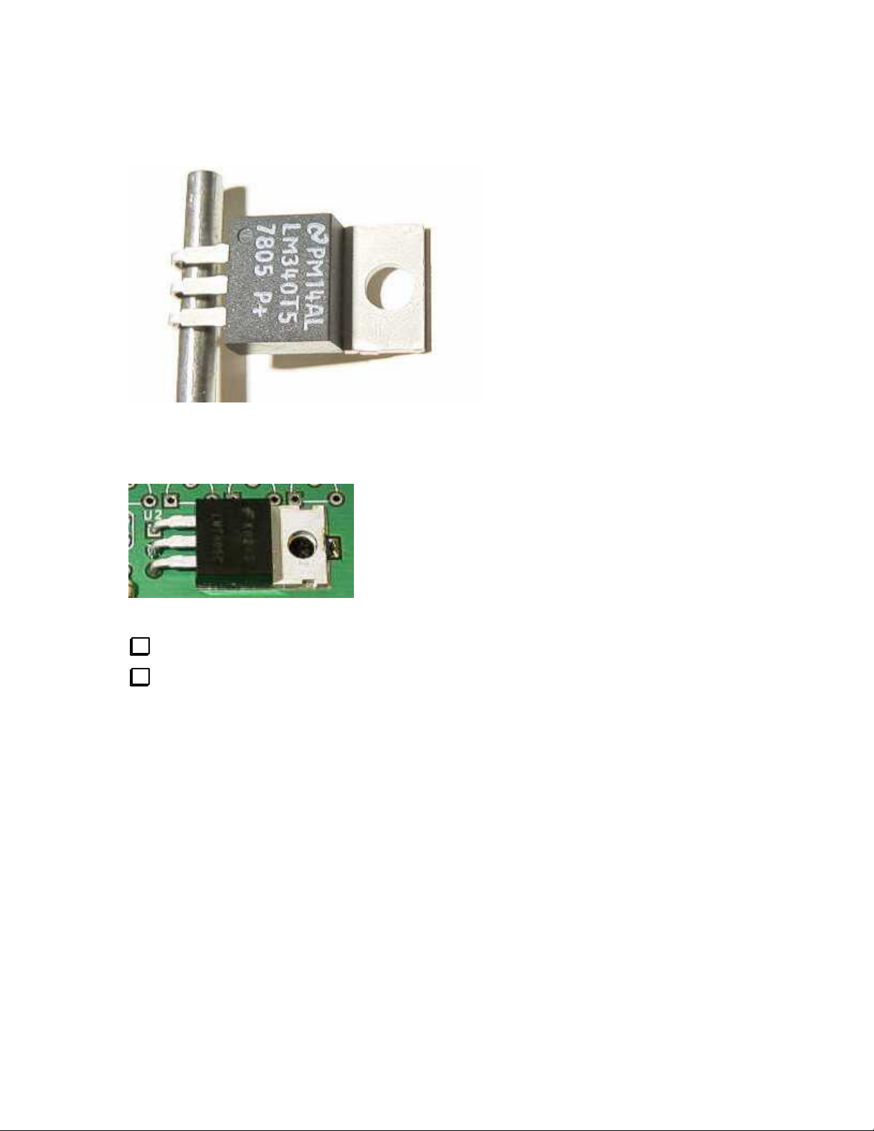
Locate U2 and match it to the PCB. Pre-bend the leads to align with the holes in the PCB while keeping
the mounting hole in U2’s tab in line with the mounting hole near the center of the PCB.
You may notice that the mounting hole area of the board near U2 has a keyhole shape isolated from the rest
of the top of the PC board, but that there are four thin traces, like the spokes of a wheel, connecting them.
This is normal - don’t cut the small traces!
You may find it helpful to use a 1/8” (0.8 mm) drill bit as a form to bend the leads of U2.
Verify the holes are aligned before you solder.
Near the center of the PCB:
U2 LM340T (LM340, 7805)
Solder the tab to the board near the end of the tab. This requires more heat than the other connections
in the board. Use a larger iron if you have one available. You do not need much solder, and DO NOT
solder near the mounting hole. The reason for soldering is to relieve mechanical stress from the leads of
U2 when the KDSP2 PCB is mounted and the mounting screw tightened
The following capacitors are ceramic monolithic with radial leads. The capacitor should sit flush to the
PCB, with exposed leads not more than about 1/32” (1mm) above the PCB.
8
Page 9
Starting near the center left hand side of the PCB:
C5 0.1 uF (104)
C8 0.1 uF (104)
C3 0.1 uF (104)
C4 0.1 uF (104)
Starting near the lower left hand side of the PCB:
C12 (skip for now)
C9 0.01 uF (103)
C13 0.01 uF (103)
C6 33 pF (33 or 330 - NOT the large, rectangular capacitor that may be marked 330n)
In the following step, pay particular attention to ensure that the leads of C7 do not extend below the bottom
of the PC board. You may find it easiest to pre-trim the leads before you solder.
C7 0.01 uF (103)
You should have one 470 pF ceramic monolithic capacitor remaining, and location C12 should be
empty.
The following capacitors are polarized. This means that it matters which lead goes into which hole on the
PCB! Take a moment to examine the electrolytic capacitors supplied. The positive (+) lead is typically
longer than the other. In addition, the negative lead side is usually marked on the case with a bold stripe.
Be sure you know which lead is the positive lead.
On the PCB, the positive lead has a square pad, and is marked with a + symbol.
There are two physical sizes of 10 uF capacitor supplied. One is much smaller than the other.
Use the small capacitors in the following two steps.
Near the bottom center of the PCB:
C10 10 uF low profile capacitor (10 uF or 106)
C14 10 uF low profile capacitor (10 uF or 106)
9
Page 10
You should have no low profile electrolytic capacitors remaining.
Install the remaining electrolytic capacitors, starting near the upper left hand corner of the PCB:
C1 10 uF (10uF or 106)
C2 22 uF (22 uF or 226)
C16 (skip for now)
You should have one 10 uF electrolytic capacitor remaining, and location C16 should be empty.
The next component is a resistor, physically larger than those previously installed. The PCB lead spacing
is 0.6” (15mm). As before, bend the leads close to, and at right angles with, the body of the resistor before
installing it on the PCB. The holes in the PCB are intentionally a little close, and the resistor may sit
slightly off the surface of the PCB.
R12 43 ohm, 2W (43 or yellow-orange-black-gold)
The next parts are in a TO-92 plastic case. These are three-legged parts. Orient the part so that the flat side
of the case matches the PCB outline. The holes in the PCB are on a 0.1” (2.5mm) grid. You will need to
carefully spread the leads on the part before installing it onto the PCB. It is important that the parts sit
fairly close to the PCB, with the top of the case not more than 0.375” (3/8” or 9.5mm) above the PCB.
This is to provide clearance for the DSPx module which will sit above the KDSP2 PCB assembly.
These parts all look very similar, but there are three different part types. You will first install the two parts
that are different than the others.
Q5 and Q6 are Field Effect Transistors, used to mute audio when required. They are sensitive to static
charges, so be sure to follow correct anti-static handling procedures when installing these parts.
Near the center of the lower edge of the PCB:
Q5 J309 FET (J309)
Q6 J309 FET (J309)
Q2 is a PNP transistor, used in driving the K2 auxbus.
Near the center of the PCB:
Note that the transistor is to the right of the legend Q2.
Q2 2N3906 (2907, 3906)
10
Page 11
The remaining TO-92 parts are NPN transistors. Q1 and Q3 are used in the auxbus interface, Q4 drives the
LED and Q7 drives the audio muting circuit.
Starting near the center left hand side of the PCB:
Q1 2N3904 (2222, 3904)
Q3 2N3904 (2222, 3904)
Q4 2N3904 (2222, 3904)
Q7 2N3904 (2222, 3904)
You should have no TO-92 style components remaining.
The next component is the ceramic resonator. This sets the operating frequency of the microcontroller. It is
not polarized - just be sure the center lead goes in the middle hole!
Near the center of the PCB:
Z1 4.0 MHz (4, 4.0 or 4.00)
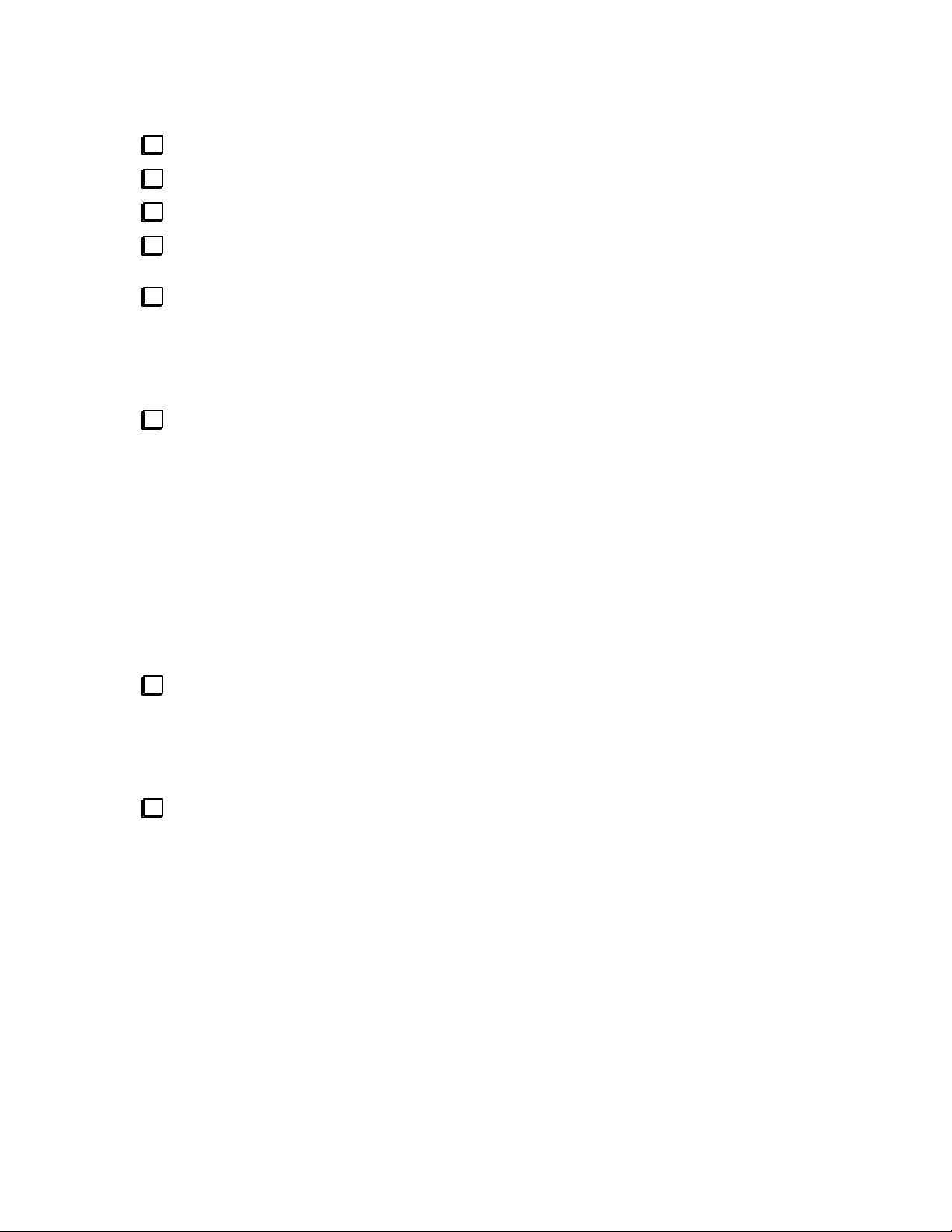
U1 is the microcontroller that operates the KDSP2. It is socketed, and you will next install the socket.
Be sure the socket pins are all through the PCB before you solder, as it is easy to bend one or fold one or
more. Also, note that the socket is polarized with a notch near the pin 1 end. The PCB silkscreen also has
a notch near the pin 1 end, which is towards the upper edge of the PCB.
When installing the socket, solder two diagonally opposite corners, then inspect the board to be sure the
socket is flush to the PCB and aligned correctly, and that all 28 pins are protruding through the PCB. Then,
proceed to solder the remaining twenty-six pins. Be sure and trim the pins on the bottom of the board after
soldering.
At location U1:
28-pin IC socket
Next is the real-time clock IC, U3. It is static sensitive, and polarized. Be sure the notch, dot or dimple
is towards the Lithium cell holder (BT1) silkscreen legend.
Near the lower right-hand corner of the PCB:
U3 NJU6355ED IC (NJU6355)
11
Page 12
Near U3 is a small, cylindrical crystal. The exposed lead length should be about 0.1” (2.5 mm). Be careful
with the crystal’s leads, as they are very thin and may break if stressed. Do not attempt to push the
crystal down flush to the PC board!
Y1 32.768 kHz crystal
As long as we are on the right side of the PCB, this is a good time to install the LED. The LED is
polarized. The shorter lead goes in the square hole on the PCB. This is opposite to the rule about
electrolytic capacitors. The lead length is the only clue as to the part’s polarity, so don’t clip until you have
verified it is installed correctly!
Near the upper right-hand corner of the PCB:
LED1 Red LED (no marking)
The 12-pin and 20-pin female connectors are next. These are the mating connectors for the DSPx module.
You may find it easiest to tack the connectors in place at two opposite ends, verify the connectors are
seated on the PCB and at right angles to it, then solder the remaining pins.
i
NOTE: The clearances are very tight in a K2/100, so the connectors must be flush to the
PCB.
12
Page 13
J1 20-pin female header (2 rows of 10 pins)
J2 12-pin female header (1 row of 12 pins)
When you install the IC in the next step, be very careful to not damage crystal Y1!
Install U1 (ATMEGA8L) into the 28-in IC socket on the KDSP2 PCB. Be sure pin 1 (the end with a
notch, dimple, or U-shaped pattern) is towards 20-pin connector J1 of the KDSP2.
Film capacitors are typically in a rectangular casing of a solid color. The part value is stamped directly on
the part. These parts are not polarized.
Near the center of the bottom edge of the PCB, adjacent to J2:
C15 0.33 uF (330n or 334)
C11 0.33 uF (330n or 334)
You should have no film capacitors remaining.
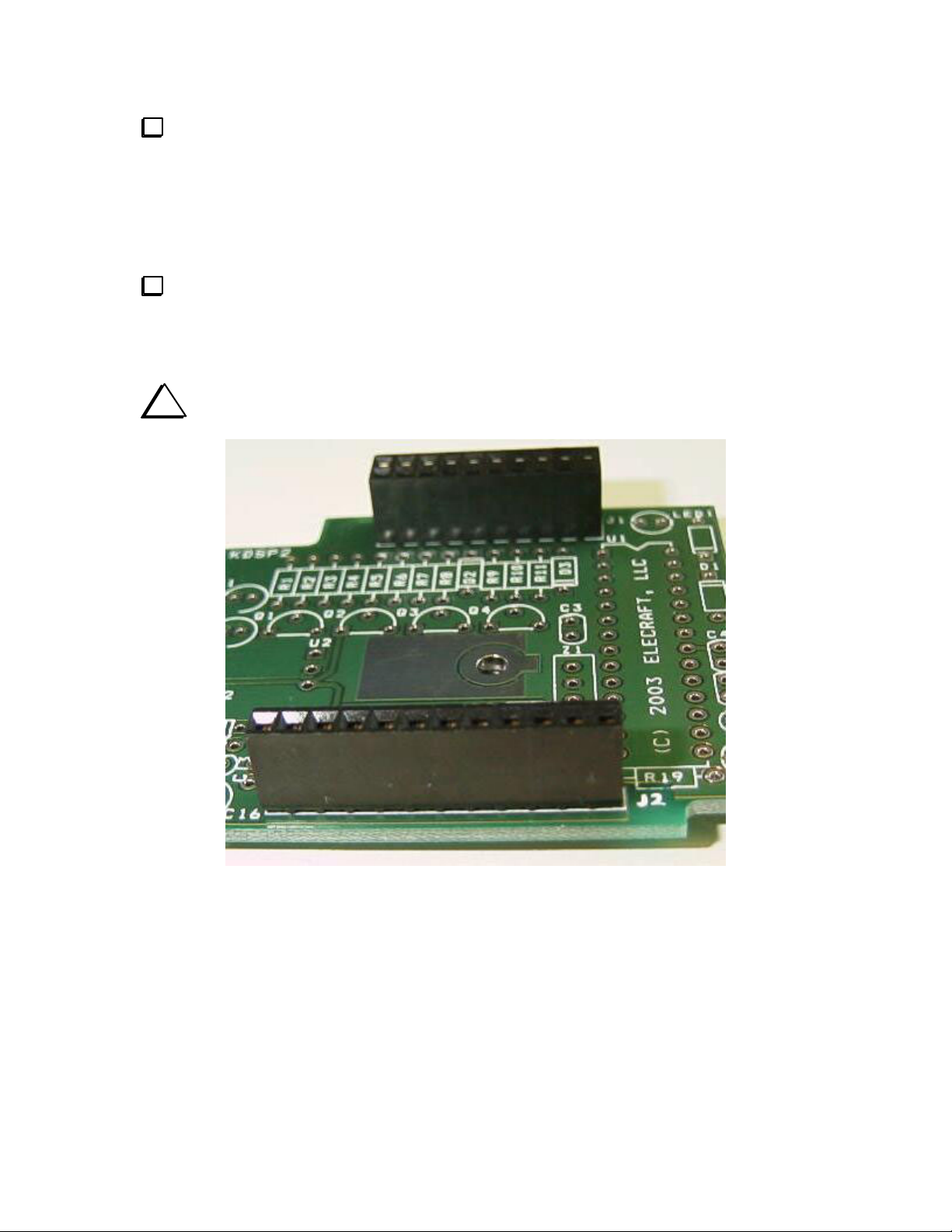
The next two connectors mount on the bottom of the PCB. They will mate with the control board in the
K2. They must be mounted flush to the PCB and they must be perpendicular to it.
13
Page 14
i
NOTE: The short end of the pins on the male headers are soldered into the KDSP2 PCB.
On the bottom of the PCB at the now-right hand side:
On the top of the board, install the final two capacitors. Remember, the electrolytic capacitor is polarized!
In the next step, you will install the three-pin Lithium cell holder on the right side of the PC board. You
need to pre-trim two of the pins so they are flush with the bottom of the PCB. The two pins that need to be
pre-trimmed are the center pin and the pin nearest diode D4.
P1 5-pin male header (1 row of 5 pins)
P2 3-pin male header (1 row of 3 pins)
C12 470 pF (471)
C16 10 uF (10 uF or 106)
Pre-trim the leads on Lithium cell holder BT1.
Install BT1, soldering all three pins. The Lithium cell will be installed later.
Verify the middle pin and the pin nearest D4 do not protrude below the bottom of the PCB
Carefully inspect the board for solder bridges (especially at the polarized capacitors and Y1), poor
solder joints, etc.
You should have only the following components remaining:
Lithium cell (CR-2032)
3-pin female header;
5-pin female header;
0.5” male-female threaded spacer;
4-40x1/4” screw
DSPx Module
Gray Foam
Black Foam
14
Page 15
Control Board Preparation
The control board of the K2 may need to be modified to accept the KDSP2. If you already have a KAF2,
no further changes are required and you may skip this section and proceed to Installation.
Verify the firmware on the Control board is at least rev 2.01. If it is earlier, contact Elecraft and obtain
current firmware. Install it and verify the radio operates properly before proceeding!
Turn off the K2.
Remove power from the K2 and disconnect antenna cables, keys, microphones and any other
accessory that is plugged in to the radio.
If you have the KBT2 option, place the switch on the rear panel of the K2 in the OFF position.
Remove the top cover from the K2. Disconnect any internal cables from the top cover to the K2,
including all cables to the Control Board. See the K2 manual for details.
Remove the two screws that secure the Control Board to the Front Panel Board inside the K2. Extract
the Control Board using the long-handled allen wrench as described in the K2 Owner’s Manual. For K2s
with S/N below S/N 3000, it is on page 40. The current manual, Rev D for kits S/N 3000 and above, has
this information on page 40 as well.
Place the Control Board on your work surface, component side up.
If your Control Board is revision A, or revision X-something, the silkscreen information for the audio
filter is on the back side of the board. Do not install anything for the audio filter on the back side of the
board. The two connectors to be added must go on the component side of the board.
i
NOTE: Removal of R18 and R19 must be done with care. DO NOT overheat the solder pads
on the PCB, tug on them with the joints hot, etc. If you lack good desoldering tools (wick,
desoldering pump, etc.) then it is best to clip the leads individually at the body of the part.
Then, using long-nose pliers, apply gentle pulling force while heating the joint with your
soldering iron. The lead will come out easily. If you have the iron on the joint more than a
few seconds and the lead won’t come out, you are doing something wrong. The Elecraft
email reflector is a good source of help for techniques, as is the Builder’s Resources section
of the Elecraft website (www.elecraft.com).
Clearing the hole of solder is best done with solder wick or a simple desoldering pump.
IT IS CRITICAL THAT THE LEADS BE REMOVED AND THE HOLE BE FREE FROM
SOLDER TO INSTALL THE CONNECTORS IN THE FOLLOWING STEPS.
hand end of the 36-pin connector, J2.
Remove R18 and R19. These may be actual resistors or wire jumpers. They are located near the right
15
Page 16

Using solder wick or a desoldering pump, carefully clean out the holes of solder where the leads of
R18 and R19 were. DO NOT overheat the pads.
Install the 5-pin female header (1 row of 5 terminals) at J1 on the component side of the Control
Board. The connector must be seated flush to the PCB and perpendicular to it. Solder the center pin only.
Install the 3-pin female header (1 row of 3 terminals) at J2 on the component side of the Control
Board. The connector must be seated flush to the PCB and perpendicular to it. Solder the center pin only.
Inspect the installation and verify the connectors are flush to the board and perpendicular to it.
Solder the remaining pins of J1 and J2.
Examine the electrolytic capacitors on the Control Board from the right hand side of the
microcontroller (U6) to the right edge of the PCB. Ensure that these parts, and any other tall parts in the
area, are firmly seated to the PCB and are straight. Clearance is tight between the KDSP2 and the Control
Board, and you must take care to ensure no shorts will develop.
Plug the Control Board into the K2 RF Board.
Installation
The Control Board is held in place with two 4-40 screws. The screw nearer J1 and J2 will be replaced with
the male-female threaded spacer provided with the KDSP2 kit.
If you have previously installed a KAF2 in your K2, remove it and skip the next two steps.
Thread the ½” (12mm) threaded spacer through the mounting hole in the Control Board nearer J1 and
J2. Tighten it snugly by hand. Do not overtighten - the spacer is made of aluminum and can be damaged
by less torque than you might think.
Verify the other mounting hole of the Control Board is secured with K2-supplied 4-40 hardware.
Remove Frequency Counter cable (used for CAL operations) if present.
Plug the KDSP2 board into the control board. Clearance between the KDSP2 and the cabinet side
panel may be very tight.
Ensure that the pins going into J1 and J2 are aligned properly. Misalignment (being off by one or
more pins in either direction) may result in damage to the K2, the KDSP2, or both. If the mounting hole in
the KDSP2 does not line up with the threaded hole in the spacer just installed, you may have the KDSP2
improperly mated with J1 and J2. Re-check.
Check that the KDSP2 board doesn’t interfere with the grounding wire on the PLL reference crystal(
X1 on the RF board). The grounding wire for this crystal should be on the side of the crystal, not the top.
If it is on the top, you should move it to the side of the crystal.
16
Page 17

Use the supplied 4-40 x ¼” screw and the original lockwasher to secure the KDSP2 to the threaded
spacer. Do not overtighten the screw - the spacer is made of aluminum and its threads can be stripped.
If your K2 is Rev B (S/N 3000 or higher), inductor L1 on the Control Board will touch the bottom of
the KDSP2. This is normal. The case of L1 is not conductive and will not cause an electrical short.
Once again, verify there are no clearance problems between the KDSP2 and the tall components on
the K2 Control Board. In particular, be sure there is clearance between the bottom of the KDSP2 PC board
and the tops of the large electrolytic capacitors on the Control Board (C28 and C29).
Using anti-static precautions, install the DSPx Module to the KDSP2. The clearances are very tight,
and you may have to rotate the DSPx Module into the KDSP2 to clear tall components on the RF Board.
Ensure the KDSP2 is completely seated on its connectors, and that it is properly aligned. Failure to
align it properly could result in damage to the KDSP2, the DSPx, or both. When installed, there is a gap of
about 1/16” (1 to 2 mm) between the KDSP2 and the bodies of the Control Board connectors. There are no
mechanical fasteners to hold the DSPx in place. It is secured by the friction of its connectors. In the final
assembly section, you will install an insulated retention system to ensure the DSPx Module does not come
loose from vibration or reasonable shock.
Turn on the K2. If you see or smell smoke or fire, turn it off immediately, find and fix the cause.
Refer to Troubleshooting.
17
Page 18

Initial Checkout
Set the K2 AF GAIN control to minimum. This is good practice whenever you turn on the K2 as there
may be a loud “POP” in the audio, a strong signal on the frequency to which it is tuned, etc.
Turn on the K2. The LED should come on briefly, then extinguish.
The LED is turned on by the DSPx upon reset. It also comes on if there is an unrecognized command
issued to it by the KDSP2 controller.
It is turned off when the DSPx receives a valid command from the KDSP2. This occurs within a second or
so after power up, after the K2 announces its mode settings to the KDSP2.
Tap the
If you are not in the secondary menus, tap
K2 display.
Rotate the K2 main tuning knob until you see
already on, by pressing
Tap
Turn up the AF GAIN control. You should hear audio.
Select CW mode.
Press, hold, then release the
MENU
MENU
button.
DISPLAY
rtc
EDIT
followed by
to exit the menus and return to the normal K2 frequency display.
AFIL
BAND+
button. The display should briefly indicate
. You should briefly see
in the K2 display. Turn it ON if it is not
.
SEC
CF2
Tap the
DISPLAY
button. You should see something like this:
C2 Nr
Congratulations! Your KDSP2 is functioning normally. Next up: Lithium cell installation.
in the
18
Page 19

3-Volt Lithium Cell Installation
Turn the K2 off.
The (+) side of the 3-volt cell must be oriented towards the DSPx module. The (-) side must face the left
side panel of the K2.
i
DO NOT use long-nose pliers to hold the Lithium cell! Doing so will short the + and - sides
together.
In the following step, be careful to not stress the spring clip when inserting the cell, or it may not make
good contact with the cell.
Insert the Lithium cell into its socket, under the spring clip.
The Operation section of this manual describes the procedure to set the clock and calendar.
19
Page 20

Final Assembly
Before re-assembling your K2 or K2/100, you need to add the self-adhesive foam retainers. These will
help protect the DSPx module in the event your transceiver is subjected to high levels of shock (Oops! You
dropped it!) or vibration (e.g., mobile installation in your off-road vehicle or helicopter).
K2
The black self-adhesive foam will be used to prevent the DSPx from disengaging from the KDSP2.
Place the K2 top cover on a soft cloth or other clean surface to protect the painted finish on the cover.
Orient the cover so that the speaker is towards you and the rear panel is away from you.
Clean the inside surface of the top cover to the right of the speaker and towards the front. Ensure it is
dry. Note that use of rubbing alcohol may leave a powdery residue that will hinder the adhesive.
The foam tape will be placed parallel to the front of the top cover. The distance from the front edge of the
tape to the front edge of the cover should be 1.5” (3.8cm). The tape will extend from the speaker towards
the right edge of the top cover. It should touch, or nearly touch, the edge of the speaker frame.
Remove the backing from the foam.
20
Page 21

Attach the foam to the top cover.
If you normally have the counter cable installed in your K2, re-install it now.
When you re-install top cover assembly on your K2, we recommend you place it down, then slide it
forward. Don’t rotate it down into place as this may tend to compress or distort the foam.
When properly installed, the foam will be just behind the DSPx module, preventing it from disengaging
from the KDSP2.
K2/100
On the forward edge of the heatsink, centered on the speaker, you will install the gray foam. This is ¼”
wide. Do not use the black foam! It is for the regular K2 cover.
Ensure the heatsink is clean.
Ensure the heat sink is near room temperature. The adhesive doesn’t work as well when it is cold.
Remove the backing from the foam.
21
Page 22

Attach the foam to the heatsink.
We recommend you not leave the frequency counter cable installed in your K2/100.
When you re-install KPA100 assembly on your K2/100, we recommend you place it down, then slide it
forward. Don’t rotate it down into place as this may tend to tear or wedge the foam.
When properly installed, the foam will be under slight compression, preventing the DSPx module from
contacting the heatsink.
22
Page 23

Operating the KDSP2
The KDSP2 is controlled by the K2’s DISPLAY, AFIL, BAND+, BAND-, RCL and STORE
buttons.
When a button is to be momentarily pressed (tapped) it is shown like this: BAND+. When a button is to
be pressed and held for a ½ a second or so, and then released, it is shown like this: RCL
The KDSP2 recognizes three modes:
C for CW;
S for SSB (it does not distinguish between LSB and USB);
R for RTTY.
The mode is determined by decoding auxbus traffic within the K2 transceiver.
For each mode, the KDSP2 maintains four filters, accessed using the AFIL button. Each time you press
the AFIL button, you cycle to the next filter. After the fourth filter, the next is the first, always cycling
through them in increasing order. If a filter is set to LPASS (low pass), then it becomes the last filter in
that mode’s sequence. You can use this to reduce the number of filters in a given mode’s sequence.
On power up, the KDSP2 will default to the first filter for each mode. It will retain the current filter for
each mode until power is again cycled.
The factory default filters are:
Mode Filter Center Width Notch Denoise Denoise Level
CW 1 LOW
PASS
2 600 Hz 800 Hz Not avail Off 1
3 600 Hz 250 Hz Not avail Off 1
4 600 Hz 100 Hz Not avail Off 1
Mode Filter Low Cut High Cut Notch Denoise Denoise Level
SSB 1 LOW
PASS
2 200 Hz 2.5 kHz Off Off 1
3 300 Hz 1.9 kHz Off Off 1
4 300 Hz 1.6 kHz Off Off 1
LOW
PASS
LOW
PASS
Not avail Off 1
Off Off 1
23
Page 24

Mode Filter Center Width Notch Denoise Denoise Level
RTTY 1 LOW
PASS
2 2.5 kHz 1000 Hz Not avail Not avail Not avail
3 2.2 kHz 300 Hz Not avail Not avail Not avail
4 1.0 kHz 200 Hz Not avail Not avail Not avail
Table 1 - Factory Default Filters
For CW and RTTY, the first column of numbers represent the bandpass filter center frequency and the
second column the width. This is because these modes are commonly tuned and referred by their center
frequency.
For SSB, the first column represents the lower frequency of the audio passband and the second column the
upper frequency of the passband. This is generally more convenient than specifying a center frequency and
width. You may think of the first column as “low cut” and the second as “high cut” in passband terms.
Filter Selection
When you select a DSP filter (by pressing the AFIL button) the mode and filter number momentarily
appear in the K2 display. For example, when going from CW filter 1 to CW filter 2, the display will briefly
show:
LOW
PASS
Not avail Not avail Not avail
CF2
To display the KDSP2’s primary menu, tap the DISPLAY button.
KDSP2 Primary Menu
In SSB or CW modes, the primary menu is used for the auto-notch and noise reduction functions. In
RTTY, the primary menu is the Filters menu, described below.
From the primary menu, you can toggle the noise reduction adaptive filter (generally referred to as a
“denoiser” and, in the SSB mode, the auto-notch filter. You can also adjust the denoiser’s level from 1
(least aggressive) to 4 (most aggressive).
Let’s assume you were in SSB mode using filter 2. Tap the DISPLAY button to bring up the primary
menu in the K2 display:
S2 nr nt
This indicates SSB mode, filter 2, denoiser and autonotch are off.
24
Page 25

To toggle the denoiser, tap the BAND+ button.
appears for a second. The “1” signifies the current noise reduction level. This display will be followed by
The decimal point preceding the nr indicates the denoiser is active. You will likely hear the difference in
the noise level coming from the K2.
When you activate the denoiser in SSB or CW modes, the denoiser remains active for all filters in that
mode until you deactivate it. When off, it is off for all filters in that mode until you activate it. Thus, you
can have the denoiser on in SSB and off in CW.
Tapping BAND+ again will turn off the denoiser.
S2 .n1 nt
S2 .nr nt
S2 nr nt
The notch, available only in SSB mode, is toggled by tapping the BAND- button.
The decimal point preceding the nt indicates the auto-notch is active. If both autonotch and denoiser were
active, you would see something like
Like the denoiser, the notch setting applies to all SSB filters.
You may adjust the level of the denoiser by pressing and holding STORE . This will cycle through the
levels. The available levels are 1,2, 3 and 4. The greater the level of the denoiser, the better it is at
suppressing noise, but it also suppresses some speech. Lower levels permit voice signals to pass through
the filter more readily, along with more noise. You should experiment with the available levels of the
denoiser under various band conditions to get a better feel for the effect of this control.
If in the above example you used the STORE button, you would momentarily see
followed by
S2 nr .nt
S2 .nr . nt
S2 .n2 . nt
S2 .nr . nt
25
Page 26

Note that the denoiser has been activated. It makes little sense to adjust the denoiser if you can’t hear the
effect, so the KDSP2 automatically enables the denoiser whenever an adjustment is made to it.
The .n2 which briefly appears informs you that the denoiser has been set to the fourth level. The display
then reverts back to .nr for better functional clarity. If you continue to press the STORE button, you will
see the filters cycle through 3, 4, 1, 2…
The denoiser levels for SSB and CW may be set independently.
If you press BAND- in CW mode, you will see something like
c2 nr
The lower-case c indicates that the alternate “soft” CW filters are in use. These filters have less skirt
selectivity than the standard filters, but offer better ultimate rejection. They also have slightly less ringing,
along with some attenuation, in the narrowest settings. Pressing BAND- again will toggle the CW filters
back to the standard ones, indicated by an uppercase C.
C2 nr
The next menu after the main menu is the Filter menu. The Filter menu is the primary menu for RTTY
mode.
You can exit this menu, and all other KDSP2 menus, by turning the VFO knob, changing mode or filter,
keying the radio, tapping DISPLAY, or holding XFIL + AGC . There are others, but these are the most
common.
To access the next menu, press RCL. You can always get to the next menu by pressing this button.
KDSP2 Filter Display
You will see a display something like this:
S. 2 . 20 2.5
This shows the mode, filter, lower and upper cutoff frequencies. In this case, it is SSB filter number 2, with
a 200 Hz lower cutoff frequency and a 2.5 kHz upper cutoff. The decimal point after the S in S2 indicates
the denoiser is active. The notch is off in this example. If it were on, the decimal point after S2 would be
on, like this:
S. 2 . . 20 2.5
26
Page 27

If a CW or RTTY filter were being displayed, the numbers represent center frequency and width, like this:
C. 2 . 60 .80
This shows standard CW filter 2, denoiser active, 600 Hz center frequency and 800 Hz width.
i
NOTE: the frequencies are always displayed as kHz with the decimal point in the appropriate
place.
once per second. During the update process, you may hear a brief noise in the audio. This is due
to auxbus traffic within the K2, and is normal. When you return to the normal K2 display, the
noise will cease.
Changing Filter Frequencies
The most common operations to be performed on a filter are to alter its frequencies.
You will notice that the leading decimal point for the second set of numbers is blinking about once per
second. This tells you that this filter value may be changed.
To change the filter value, tap the BAND+ or BAND- buttons. If you tapped the BAND+ button, you
would see
i
NOTE: when the KDSP2 is taking over the K2 display for its various menus, the display updates
S. 2 . 20 2.4
Tapping the BAND- button would return the filter to its previous state
S. 2 . 20 2.5
To change the other numbers, in this case the SSB low-cut frequency (center frequency in CW or RTTY),
press and hold the STORE button. The blinking decimal point will move to the first set of numbers. You
may increase or decrease the indicated value by tapping BAND+ or BAND- . Tapping the BAND-
button with the above displayed would yield
S. 2 . 15 2.5
Other modes operate in the same fashion.
27
Page 28

There is a special filter for each mode, called LPASS (for low pass). This filter widens out the passband so
you can more easily eavesdrop on neighboring frequencies. In CW, the filter is from a few tens of Hertz to
2.5 kHz; in SSB to 3.0 kHz; in RTTY to 3.5 kHz.
To invoke this filter in SSB, increase the high-cut frequency to its maximum limit (3.0 kHz) and reduce the
low-cut to its minimum (.00 kHz). You will then see
S. 2 LPASS.
To change from this special filter, just tap BAND- or BAND+ . As with the other displays in this menu,
there will be a blinking decimal point.
In SSB mode, the LPASS filter is selected by increasing the high cut to its maximum value (3.0 kHz) and at
the same time setting the low cut to its lowest value (.00 kHz).
In CW and RTTY modes, it is selected by setting the highest center frequency and the widest bandwidth.
Saving New Filters
What if you want to change a default filter and retain it through the next power cycle of your K2?
The KDSP2 includes EEPROM memory to allow you to do just that. In fact, every time you make a
change to any KDSP2 setting, it is automatically saved into EEPROM. No special steps are required
Bypassing the KDSP2
Return to the DSP display by tapping DISPLAY . If the denoiser is active, tap BAND+ to kill it.
Press the RCL button. You will see the Filter menu display:
S. 2 LPASS
Tap BAND- or BAND+ to drop from the LPASS mode, and using the buttons you have learned, return
the display to:
S. 2 . 20 2.5
Press the RCL button. You will be advanced to the Bypass Menu. It looks like this:
You have the capability of bypassing the KDSP2 functions, which significantly reduces the power
consumption of the KDSP2. If you tap BAND-, you will hear a change in audio and you will see
dsp 0n
28
Page 29

dsp byP
When the DSP is in bypass mode, if you invoke the DSP display (by tapping the DISPLAY button) you
will always be sent to this menu so you can quickly turn the DSP filters back on.
Simply tap BAND+, and you will return to DSP ON. The display will flash something like:
d2 .nr nt
The “d” indicates the DSP is being synchronized to the K2 current mode and filter selection. About one
second later you’ll see
S2 .nr nt
or whatever the main menu display is for the current mode and filter you have selected.
i
NOTE: There may be brief drop, or “hole”, in the audio when you toggle between DSP ON and
DSP BYPASS modes. This is normal. It is a result of muting the audio briefly to allow the audio
levels to stabilize in the KDSP2. Otherwise, you might hear an annoying “pop.”
You may also reach the Bypass menu from the K2 RTTY mode. The RTTY mode is enabled by a K2
secondary menu in version 2.x firmware and later. It will be the next menu after the Main menu - the
denoiser menu does not apply to the RTTY mode as it could add distortion to the signal, making data
harder to decode.
Return to the Bypass menu:
If you press the STORE button, you will be returned to the Main menu.
If you press the RCL button, you will be taken to a Denoiser menu (CW or SSB mode) or the Gain menu
(RTTY mode).
dsp 0n
29
Page 30

Denoiser Menus
In this menu, the nr characters indicate the denoiser, or noise reduction, menu. The first number indicates
the Beta, or aggressiveness, of the filter and the second number affects the hold time, or decay rate of the
filter. The value shown is the factory default.
As you have probably guessed, the flashing decimal point indicates the parameter (number) that will be
changed by tapping either BAND button. To adjust the other set of numbers, use the STORE button
The beta number seems to have a mild effect, especially with the noise reduction level set to 1. The decay
value seems to have greater effect, especially with smaller numbers. Experiment!
Each value has a range from 00 to 99. The value wraps around, so if you press BAND+ while 99 is
displayed, you will next see 00. Similarly, pressing BAND- with 00 displayed will take you to 99. You
should definitely hear the effect of this change!
As with all menus, the RCL button will take you to the next menu in the sequence. This will be the
Autonotch menu if the K2 is in SSB mode. If in CW mode, you will be taken to the Gain menu.
Autonotch Menu
If you are in SSB mode, and you press RCL from the Denoiser menu, you will see
This is the Autonotch menu. Like the Denoiser menu, the first number represents Beta and the second
number decay. The value shown is the factory default.
Like the Filter and Denoiser menus, the flashing decimal point indicates the parameter (number) that will
be changed by tapping either BAND button. To adjust the other set of numbers, use the STORE button
Pressing RCL will take you to the Gain menus.
Gain Menus
There are five Gain Menus available in the KDSP2. Their purpose is to allow you to balance the gain of
the system for the types of signals you most listen to. Three of the menus are based on mode (CW, SSB or
RTTY) and two are related to the Denoiser function.
The SSB Denoiser Gain menu looks like this:
nr 89 71
nt 39 07
Sn G 7.0
30
Page 31

while the CW Denoiser menu looks like this:
The Filter Gain menus are prefixed:
Cn G 0.0
CF for CW Filter
sf for SSB Filter
rF for RTTY Filter
The numbers indicate the gain setting in dB. The setting may be changed in 0.5 dB steps, from -5.5 to
+18.0.
To increase the setting, tap the BAND+ button. To decrease it, tap the BAND- button.
If you press the RCL button, you will be taken to the next menu, either a Gain menu or the Main menu for
the current mode. Pressing the STORE button will display the firmware versions of the KDSP2 (see
below) followed by the main menu for the current mode.
The Gain menus available, by mode are:
Mode Gain Sequence
RTTY RTTY
CW Denoiser, CW
SSB Denoiser, SSB
You sequence to the next Gain menu, if any, by pressing RCL. If you are at the last Gain menu, you will
go to the current mode’s Main menu.
Displaying KDSP2 Firmware Revision
If you press the STORE button in any GAIN menu, you will see the firmware revisions of the DSP and
KDSP2 controller. It will look like this:
which indicates the DSP Flash firmware version is 3.16, followed two seconds later by
dsp 03.16
CtL 03.00
31
Page 32

indicating the KDSP2 microcontroller firmware version. In this example, it is 3.00. If the MCU firmware
is prior to version 3.00, you will be returned to the KDSP2 main menu two seconds later. If the MCU
firmware version is 3.00 or later, then after another two seconds you will see a Flash memory checksum
followed by the EEPROM checksum
Two seconds later, you will be returned to the KDSP2 main menu. The numbers you see may be different,
as the firmware versions evolve.
FCS FFAd
EEP 8AC1
Filter Status Display
The K2 provides a filter status display, invoked by holding XFIL + AGC . This displays the current
XFIL and AFIL settings. For example, in CW mode, you might see
followed by
The second display is Audio Filter and number. This display does not distinguish between modes, showing
the DSP filter as AF rather than CF, SF, or RF.
FL2 0.7c
AF1
i
NOTE: The AF portion of the Filter Status Display will display only if you have pressed the
AFIL button at least once since you turned the K2 on. If the AFIL button has not yet been
pressed, the Filter Status Display will only provide XFIL information.
mode you used in which you pressed the AFIL button. Thus, when changing modes, the Filter
Status Display loses synchronization with the KDSP2 and may display incorrect AF information..
i
NOTE: When you change modes, the Filter Status Display will show the AF value of the last
32
Page 33

Real-Time Clock Menus and Displays
In addition to the DSP functions, the KDSP2 includes a real-time clock (RTC) function. The clock
provides time and date information, and includes a Lithium backup cell. The real-time clock chip monitors
the status of the Lithium backup cell. If the voltage is below limits, the time and calendar displays will be
filled with E
This means the cell voltage is low. When you first construct the KDSP2, or after replacing the cell,
this display will also be seen. Simply follow the clock and calendar setting procedure to erase the E’s. If
the cell voltage is low, the cell needs to be replaced.
From any DSP menu, you may enter the clock menus by pressing and holding STORE + RCL . This
brings up the time display in standard 24-hour format:
To display the calendar, tap either BAND button:
After about two seconds, the display will return to time.
Pressing STORE will return you to the primary DSP menu for the current mode.
If the DSP is not in bypass mode, you may change the calendar format. To do this, press RCL . You will
see either:
Tap either BAND button to toggle between these modes. The selected mode is saved in EEPROM to
remember your preferred format.
Press STORE to return to the calendar display for two seconds, followed by the time display.
Setting the Real-Time Clock
If you wish to change the time or calendar settings, make sure the DSP is not in bypass mode. Enter the
calendar format menu as described above, then press RCL .
Ee.ee.ee or ee-ee-ee
14.11.07
i
NOTE: If instead you see a display of five dashes, you weren’t in a DSP menu.
04-22-03 (MM-DD-YY format) or 22-04-03 (DD-MM-YY format).
MM-dd-YY or dd-MM-yy
33
Page 34

yr 03
Adjust the year by tapping BAND+ to increase or BAND- to decrease. The display will wrap around
between 99 and 00.
To adjust the month, press RCL .
Adjust the month by tapping BAND+ to increase or BAND- to decrease. The display will wrap around
between 12 and 01.
To adjust the date, press RCL .
Adjust the date by tapping BAND+ to increase or BAND- to decrease. The display will wrap around
between 31 and 01. Yes, you can set February to 31 days if you wish. The calendar doesn’t check to see if
the date is valid for a given month, but it does keep track accurately when it moves from month to month as
time passes.
To adjust the time, press RCL .
Adjust the hour by tapping BAND+ to increase or BAND- to decrease. The display will wrap around
between 59 and 00. The time is always in 24-hour format. There is no option for AM or PM display on a
12-hour display.
To adjust the minute, press RCL .
Adjust the minute by tapping BAND+ to increase or BAND- to decrease. The display will wrap around
between 59 and 00.
Whenever you adjust any of the time or date settings by tapping BAND+ or BAND- , the clock will reset
seconds to zero. This is handy for syncing to a time broadcast, such as WWV.
From any calendar or time setting menu, pressing STORE will take you to the time display. You may
also press RCL from the minute menu to return to the time display.
MM 04
dt 22
Hr 14
nn 11
34
Page 35

Menus Summary
Mode Current Menu Next Menu
CW Main Filter
Filter Bypass
Bypass Main
SSB Main Filter
Filter Bypass
Bypass Main
RTTY Filter Bypass
Bypass Filter
Table 2 - Primary Menu Sequences
Menu
Main* Toggle Denoiser Toggle Autonotch** Next Menu *** Decrease Denoiser
Filter* Increase Width or
Bypass DSP On DSP Bypass Denoiser, or Gain*** Main Menu
Denoiser Increase Decay or
Autonotch Increase Decay or
Gain Increase Gain Decrease Gain Next Menu *** Firmware Version
* Filter is the primary menu in RTTY mode; Main in CW and SSB modes
** Only in SSB
*** Selection is mode dependent
BAND+
Center Frequency
(Upper or lower
cut in SSB)
Beta
Beta
BAND-
Decrease Width or
Center Frequency
(Upper or lower cut
in SSB)
Decrease Decay or
Beta
Decrease Decay or
Beta
Table 3 - Button Meaning by Menu
RCL STORE
Level
Bypass Menu Toggle functions of
BAND buttons
Next Menu *** Toggle functions of
BAND buttons
Next Menu *** Toggle functions of
BAND buttons
35
Page 36

Mode Current Menu Next Menu
DSP Time Calendar Format
Calendar Format Year
Year Month
Month Date
Date Hour
Hour Minute
Minute Time
Bypass Time Time
Table 4 - Real-Time Clock Menu Sequence
Menu
Time Calendar Menu Calendar Menu Calendar Format** DSP Main Menu*
Calendar Time Menu Time Menu Calendar Format** DSP Main Menu*
Calendar
Format
Year Increment Year Decrement Year Month Menu Time Menu
Month Increment Month Decrement Month Date Menu Time Menu
Date Increment Date Decrement Date Hour Menu Time Menu
Hour Increment Hour Decrement Hour Minute Menu Time Menu
Minute Increment Minute Decrement Minute Time Menu Time Menu
* Filter is the primary menu in RTTY mode; Main in CW and SSB modes
** Only when DSP is active; otherwise sends you to DSP BYPASS Menu
BAND+
Toggle Format Toggle Format Year Menu Calendar Menu
Table 5 - Real-Time Clock Button Meaning by Menu
BAND-
RCL STORE
36
Page 37

Table 1 from the beginning of this section is repeated here for the factory default filter settings.
Mode Filter Center Width Notch Denoise Denoise Level
CW 1 LOW
PASS
2 600 Hz 800 Hz Not avail Off 1
3 600 Hz 250 Hz Not avail Off 1
4 600 Hz 100 Hz Not avail Off 1
Mode Filter Low Cut High Cut Notch Denoise Denoise Level
SSB 1 LOW
PASS
2 200 Hz 2.5 kHz Off Off 1
3 300 Hz 1.9 kHz Off Off 1
4 300 Hz 1.6 kHz Off Off 1
Mode Filter Center Width Notch Denoise Denoise Level
RTTY 1 LOW
PASS
2 2.5 kHz 1000 Hz Not avail Not avail Not avail
3 2.2 kHz 300 Hz Not avail Not avail Not avail
4 1.0 kHz 200 Hz Not avail Not avail Not avail
Table 6 - Factory Default Filters
The other defaults are:
Denoiser Beta 89
Decay 71
CW Gain 0.0 dB
Autonotch Beta 40
Decay 07
SSB Filter Gain 0.0 dB
CW Filter Gain 0.0 dB
RTTY Filter Gain 0.0 dB
LOW
PASS
LOW
PASS
LOW
PASS
SSB Gain 7.0 dB
Not avail Off 1
Off Off 1
Not avail Not avail Not avail
Table 7 - Other Factory Defaults
37
Page 38

Troubleshooting
General
If your symptoms are not covered below, check the orientation of all components, connectors and wiring.
Look especially for cold or poor solder joints. Check all DC voltages (see DC voltage chart).
Receiver noise heard when Clock or DSP menus displayed.
This is normal. The main microcontroller in the K2 polls the KDSP2 for information to display about once
per second, waking up all option module processors, which generates noise that is audible at some
frequencies. The K2 does not mute the audio under this circumstance, because you may be listening to a
signal, or wish to synchronize the clock with WWV or some other time standard broadcast. If you wish to
leave the clock display on for long periods of time, simply turn down the receiver’s AF GAIN control or
use the squelch menu entry (SLCH in the K2 secondary menu).
Error messages.
If you see not inst in the K2 display when you press AFIL or tap DISPLAY, the KDSP2’s
microcontroller (U1) may not be functioning. Make sure it isn’t installed backwards. Also check for bent
pins, check voltages on all pins, etc. Remove and re-install U3 in case dirt, dust or other problems are
interfering with good electrical contact between the IC and the socket. Try turning power off and back on.
AFIL works but I can’t access DSP or clock menus when I press DISPLAY.
The auxbus has lost synchronization. Turn the K2 off and then on again and it should clear. Please let us
know if this happens frequently in your radio.
Loud audio POP when K2 turned on.
If this is much louder than the normal turn-on transient when powering up the K2, set the AF GAIN control
to minimum and cycle power again. If the POP is only present when the AF GAIN control is advanced, it
may indicate the muting circuitry is not working properly on the KDSP2. Check R14, R19, Q5, Q6, Q7
and C8. Also check that U1 pin 14 is not bent or folded under the chip.
Weak or no audio at some filter settings.
If the KDSP2 filter is set to a frequency outside the XFIL range of the K2, it is normal for little or no audio
to be heard. Be sure your XFIL setting and BFO frequency are such that audio will be present in the
selected KDSP2 filter setting.
Filters don’t seem to be at the right frequency or pitch.
If the KDSP2 seems to work OK but some filters don’t seem to be at the correct pitch, try this test. Set the
K2 to its widest filter setting in CW mode. Connect an antenna and find a noisy band or use a noise
38
Page 39

generator. Set the KDSP2 to 400 Hz center frequency and 300 Hz width. Turn up the AF GAIN until you
hear filtered background noise. Now, increase the center frequency of the filter. The noise pitch should
increase. If the pitch does not increase with each increases in indicated center frequency, there may be a
problem in the DSPx module. If the pitch increases, but then the noise suddenly becomes weak or absent,
you are probably beyond the passband of your current XFIL setting.
If this test shows a problem with the DSPx module, you may carefully remove and then re-install the Flash
memory chip in the socket on the DSPx board. Pay careful attention to the orientation of the Flash chip in
the socket before you remove, and re-install it in the same orientation. This is a polarized part, and
reversing it may damage the DSPx module or the Flash chip. If you are uncomfortable doing this, contact
Elecraft.
LED remains on.
The KDSP2 LED will normally come on at power up, then extinguish after a second or two. If it stays on,
it indicates that KDSP2 U1 and the DSPx module are not communicating properly.
Check U1, D3 and verify that the DSPx module is properly aligned and fully seated into its two connectors
on the KDSP2 module. It is easy to be off by one pin in the alignment of these connectors. Also make sure
that both rows of pins are inserted into J1.
Clock time doesn’t increment.
U3 may be installed backwards or is defective. The 32.768 kHz oscillator may not be running- check Y1
and C6. If you have a frequency counter or oscilloscope, probe U3 pin 3 and look for a 32.768 kHz
waveform.
Clock doesn’t keep time with K2 power turned off.
Make sure the Lithium cell is installed correctly. (Nothing will be damaged if the Lithium cell is installed
backwards, thanks to diode D4.) If you suspect the cell is bad, measure it with a voltmeter and replace it if
the voltage is less than about 2.5 volts.
39
Page 40

DC Voltage Chart
Voltages are approximate. Measurements were made under the following conditions: 13.8 VDC power
supply. K2 turned ON, 3V Lithium cell installed, CW mode with default CF1 filter setting (800 Hz center,
600 Hz wide, noise reduction OFF), display showing frequency, DSPx module removed. KNB2 and KSB2
options installed.
Integrated Circuits
Pin V Pin V Pin V Pin V Pin V
U1-1 3.6 U1-11 4.9 U1-21 5.0 U2-1 13.5 U3-1 0
2 4.9 12 0 22 0 2 0 2 0.5
3 5.0 13 0 23 0 3 5.0 3 0.6
4 4.9 14 5.0 24 0 4 0
5 0 15 0 25 0 5 0
6 4.9 16 0 26 0 6 0
7 5.0 17 0 27 0 7 0
8 0 18 0 28 0 8 4.9
9 0 19 0
10 0 20 5.0
Diodes and Transistors
Pin V Pin V Pin V Pin V
Q1-B 0 Q4-B < 0.3 Q7-B < 0.3 D3-A 0
E 0 E 0 E 0 D3-C 0
C 5.1 C > 3 C 5.0 D4-A **
Q2-B 5.1 Q5-G 5.0 D4-C 4.9
E 5.0 S 5.0 D1-A 5.0 D5-A *
C 5.7 D 5.0 D1-C 4.9 D5-C *
Q3-B 0 Q6-G 5.0 D2-A 4.9 D6-A *
E 0 S 5.0 D2-C 5.7 D6-C *
C 5.7 D 5.0
*- This is a floating connection, not referenced to ground.
** - Varies with Lithium cell voltage
40
Page 41

Theory of Operation
N
N
ADC
The DSP process flow is shown above. Incoming signals are digitized at a 16 kHz rate. The samples are
then decimated, a process to provide higher performance filters with fewer coefficients. In the KDSP2,
decimation by 2 is performed, limiting the highest frequency to a little under 4 kHz.
At the output of the decimator is a bandpass filter, selected by the user for the desired characteristic.
The output of the mode-selected decimator/filter is then passed to the notch filter. This uses an LMS (leastmean-squares) algorithm. A signal is always applied to the notch filter, even if it is not enabled, to
minimize “popping” if it is selected after having been idle.
The denoiser accepts input from either the notch filter (if the notch filter is selected) or from the decimator
(if the notch filter is not selected).
The output DAC receives its information from the appropriate decimator/filter, the denoiser, or the notch.
Decimate
by 2 and
Filter
otch
oise
Reduction
(denoise)
DAC
41
Page 42

Circuit Description
The KDSP2 is an interface board that adapts the DSPx Module for internal operation in an Elecraft K2
Transceiver.
Please refer to the schematic for the following discussion.
KDSP2
Audio Path
Differential audio from the K2 Product Detector is supplied to the KDSP2 via 5-pin connector P1, pins 1
and 2. The audio is AC-coupled to the DSPx module inputs via capacitors C11 and C15. Resistors R15
and R16, along with capacitor C9, provide a simple low-pass filter to help suppress IF and RF feedthrough.
Diodes D5 and D6 act as a limiter to prevent excessively strong signals from overloading the DSP section.
These diodes will normally only provide limiting if the K2’s AGC is OFF and a very strong signal is
received. With AGC ON, the diodes should never conduct.
After processing, the differential audio is made available from the DSPx and is applied to capacitors C10
and C14. These couple the signal through muting transistors Q5 and Q6 to the K2 at P2, a 3-pin connector.
R17 and R18 provide bias from filtered +5VDC to simulate the source normally seen by the K2 audio
system.
+5V (VCC5), filtered by R13, C13 and C16, is used for the bias source.
Q5 and Q6 are N-channel JFETs with a low pinchoff voltage. Under normal operation, R14 biases the
gates of these transistors to the 5-volt bias source, and the transistors are on, providing an audio path. The
audio may be muted if transistor Q7 is turned on by applying a positive voltage to R19. When on, Q7 pulls
the gates of Q5 and Q6 low, turning them off and muting the audio signal. When the voltage to R19is
returned to 0, Q7 is turned off and capacitor C8 charges through R14. This charging action turns on the
JFETs over a period of several tens of milliseconds, to ensure there is no “pop” or other disturbing artifact
as a result of un-muting.
Power System
Incoming +10 to +15 VDC is applied through R12 and C2 to U2, an LM340T linear regulator. This is a
linear regulator so R14 shares the load with U2. A switching regulator might introduce noise into the K2 the AGC IF is on the control board and is a wideband, untuned amplifier looking at a nominal 150 kHz
signal. The maximum load current on the 5 volt regulator is about 70 mA. The output of U2 is filtered by
C1 as well as various 0.1 uF capacitors distributed throughout the KDSP2.
VCC5 is further filtered for the audio bias, described above.
42
Page 43

Auxbus Interface
The K2 auxbus operates at a nominal 5V, but may be as high as 6V with some accessories. This is
incompatible with the 5V microcontroller used in the KDSP2. Level translation is accomplished by Q1-Q3
and associated circuitry.
Incoming auxbus data is filtered by C12 and applied via R8 and D2 to an input pin on the microcontroller,
U1. R9 serves as a weak pull-up for this input. D2 is a Shottky diode, having very low voltage drop. It is
used to couple the low-level (logic “0”) signals into U1. D2 and R9 combine to limit the input high levels
(logic “1”) to +5V. This protects U1 from the potential +6V levels on the auxbus.
Q1 and Q3 are normally biased off by a LOW output from U1 to their respective bases through R3 and R4,
respectively. Q1 being off allows R2 to bias Q2 off. As a result, the auxbus drivers from the KDSP2 are in
the OFF, or high-impedance, state.
If the KDSP2 needs to assert an auxbus level of HIGH, it turns on Q1, which turns on Q2 and pulls R7 to
+5 VDC. This high level is passed through R6 and R7 to the auxbus.
If the KDSP2 needs to assert an auxbus level of LOW, it turns on Q3, whose collector is tied to the auxbus
through R6 and R8.
The microcontroller always turns OFF both Q1 and Q3 before turning either ON, to prevent contention.
R6, R7 and R8 serve as current limiters in case of an auxbus fault.
Microcontroller
U1 includes a CPU, Flash program memory, EEPROM and RAM, along with I/O ports and timers. Flash
stores the program, EEPROM the constants and filter settings.
Z1 controls the clock of U1, setting it to a nominal 4 MHz, the same as most other microcontrollers in the
K2.
U1 monitors auxbus activity, interprets button presses, manages the menus and displays, and controls the
DSPx Module.
Because the DSPx module operates internally at 3.3V (see below), it must be protected from the 5V output
of U1. Shottky diode D3 provides this isolation, allowing U1 to pull J1 pins 11 and 12 to near ground, but
preventing them from being driven to 5V. A pull-up resistor to +3.3V is included in the DSPx module to
limit the applied level when U1 pin 3 goes high.
The LED is operated directly by the DSPx Module via Q4, and is used for status information.
43
Page 44

Real-Time Clock
U3 is a real-time clock chip, incorporating clock and calendar functions. Y1 establishes the oscillator
frequency of 32.768 kHz, with C6 to act as a fine adjustment.
U1 communicates with U3 over a 4-wire serial bus. This is used to set the time and date, and read them
back.
The clock runs even when the K2 is powered off. Lithium cell BT1 provides a nominal 3V level to operate
U3 via Shottky diode D4. When the K2 is operating, +5V is supplied to the clock via Shottky diode D1.
Under this circumstance, the Lithium cell is idle. Shottky diodes are used to minimize voltage drop.
Capacitor C7 provides decoupling of the power supply to U3.
DSPx
The DSPx schematic is on a separate sheet.
Incoming +3.6 to +5.5 VDC is applied to voltage regulators U1 (supplies +3.3V for digital circuitry) and
U8 (supplies +3.3VDC for analog circuitry). U2 provides +1.8 VDC for operating the DSP core and the
CODEC core.
Incoming audio is applied to U6, a TLV320AIC23 CODEC (encoder-decoder), which contains a pair of 16bit analog-to-digital (ADC) and digital-to-analog (DAC) converters, as well as gain controllable amplifiers
and a pair of serial interfaces.
U5, an Analog Devices® ADSP-218xN series DSP chip, controls the CODEC (via U9, a Xilinx complex
programmable logic device, or CPLD). It also has a serial interface that, with suitable modification through
the CPLD, accepts ADC information and provides data to the DAC.
The program for the DSP is contained in the Flash memory, U3. At boot-up, the DSP fetches its program
from the Flash, and then runs the program from internal memory. The Flash memory also contains
numerous coefficient files for the various filters. These are fetched from the Flash on an as-needed basis.
The DSP is clocked by a 40 MHz oscillator, consisting of resonator RES1 and amplifier U4. This results in
an internal instruction rate of 80 million instructions/second.
At power up, U7 provides a reset signal of sufficient duration to allow the DSP clock systems to operate
and settle.
44
Page 45

Glossary
The KDSP2 introduces DSP technology to the Elecraft K2 transceiver line. There are many terms used that
are not familiar to many Amateur radio operators. This Glossary may be of help to you in understanding
these terms in the context of the KDSP2.
Adaptive Filter
An adaptive filter is one which continuously adjusts its characteristics automatically. In the KDSP2, two
types of adaptive filters are provided: autonotch and denoiser. These filters use an LMS algorithm to
suppress heterodynes (notch) or random noise (denoiser). See coefficients.
ADC
Analog to Digital Converter. This is a device which accepts an analog signal and converts it to a digital
value. In the KDSP2, the ADC accepts the signal from the K2 product detector and converts it to a 16-bit
digital value. It does this 16,000 times per second.
Algorithm
The step-by-step process followed to perform a particular task. In the case of DSP, the task is handled by
instructions to the DSP chip, known as software (if stored on a disk) or firmware (if stored in permanent or
semi-permanent memory)
Autonotch
Automatic notch filter. This type of filter attempts to reduce the strength of a very narrow range of
frequencies, typically caused by a carrier from a nearby station.
Beta
In the LMS algorithm, Beta defines how quickly the adaptive filter makes adjustments in its attempt to
implement the algorithm. If you think in terms of an automatic gain control, it corresponds to the attack
time.
A higher value means a more aggressive, or faster, attack.
CODEC
Coder-decoder. In DSP system, the CODEC contains an ADC and a DAC at a minimum. In the KDSP2,
the CODEC contains two ADCs, two DACs, programmable gain amplifiers, interface logic and power
management circuitry.
45
Page 46

Coefficients
In mathematics, the coefficients of an equation are usually constant values. For example, in the phrase
Ax
2
+ Bx + C
A, B and C are coefficients. x is the variable.
In DSP filters, the coefficients define the filter response, and are usually fixed (constants). The sampled
signal is the variable, and the result of the equation is the filtered signal.
In the case of adaptive filters, the coefficients are changed by the DSP as a result of computations, so are
not really constants.
DAC
Digital to Analog Converter. This is a device which accepts a digital value and converts it to an analog
voltage. In the KDSP2, the DAC accepts the16-bit digital information from the DSP chip and converts it to
a differential analog voltage which is applied to the audio amplifier in the K2. It does this 16,000 times per
second.
Decay
In the LMS algorithm, Decay defines how quickly the filter abandons adjustments made in its attempt to
implement the algorithm. If you think in terms of an automatic gain control, it corresponds to the decay
time.
A higher value means more rapid decay.
Decimation
It is sometimes advantageous to reduce the sampling rate of a signal that has already been sampled. The
process of doing this is called decimation. In the KDSP2, the input sampling rate is 16 kHz. The filters
operate better with a sampling rate of 8 kHz. A “decimation by two” operation takes place to change the
sampling rate to 8 kHz from 16 kHz.
Denoiser
A process to remove random noise from a signal. This is usually meant to be thermal noise like the
background hiss of an HF band. Denoisers usually don’t do well against static crashes or impulse (ignition)
noise.
46
Page 47

DSP
Digital Signal Processing. This is a system that accepts signals that are digitized, and performs operations
on them, such as filtering. In the context of most Amateur radio equipment, the term DSP often applies to
the whole accessory, like the KDSP2, and is taken to include the analog-to-digital and digital-to-analog
conversions as well.
FIR
Finite impulse response. This is a basic filter structure which does not use feedback. As a result, it cannot
oscillate. FIR filters are common in DSP work, but very rare in analog design. FIR filters usually need
much greater length to get similar results to an IIR filter, but FIR filters are often much better behaved.
They have controlled phase characteristics, less ringing, and so forth.
In the KDSP2, all filters are FIR filters.
See also IIR.
Gain
This indicates the amount of amplification, or attenuation, of a signal. In the KDSP2, various GAIN menus
are available. Their purpose is not to increase the gain of the overall K2 system. Rather, they are provided
to balance the gain between the various modes and functions. For example, assume you have SSB Gain set
to 4.5, CW gain to 3 .0 and RTTY gain to 5.0. They should all be reduced by 3.0. This will result in
settings of 1.5, 0.0 and 2.0, respectively. When doing gain balancing, one of the gains should be 0.0. The
Sn and Cn menus are to accommodate a possible loss of signal strength when the denoiser is active.
IIR
Infinite impulse response. This is a basic filter structure which uses feedback. As a result, it can oscillate
and ring. Nearly all op-amp and switched-capacitor filters in common use are IIR. Some DSP filters are
IIR, as these filters require far less computation for a given response. IIR filters often cannot provide
desired phase and amplitude response characteristics, and are only used in DSP systems in certain special
cases.
The KDSP2 does not use IIR filters.
See also FIR.
Interpolation
This is a process where a signal that was sampled at a lower rate is made to appear as if it were sampled at
a higher rate. In the KDSP2, the autonotch and denoiser operate at a 16 kHz rate, but the filter that
precedes them is running at 8 kHz. An “interpolate by two” operation is used to convert the lower
sampling rate to the higher one.
47
Page 48

Length
In DSP, filters consist of two blocks of memory. One holds the coefficients, and the other the sampled
signals. The size of these two memory blocks are the same, and are usually referred to by their length,
measured in taps. The longer the filter, the more taps it has, and the more precise it can be. Thus, longer
filters usually have steeper sides, less ripple, or more attenuation – or some combination of all three.
Longer filters also have greater delay, and require more processing power to implement.
LMS
Least Mean Squares. This is an algorithm that is widely used in adaptive filters. The two adaptive filters in
the KDSP2 are the autonotch and the denoiser.
Sampling
When signals are digitized, they are said to be sampled. In the KDSP2, analog signals from the K2 product
detector are sampled at a 16 kHz rate. This means that 16,000 times per second, the output voltage from
the product detector is converted to a 16-bit digital value by the ADC and fed to the DSP.
Taps
Each memory location used by a DSP filter is usually referred to as a tap. Thus, a filter using 100 memory
locations for its signal samples would be said to have 100 taps. The term is historic and comes from the
concept of a delay line, which was an L-C network that literally had “taps” along its “length.”
48
Page 49

49 50
Page 50

 Loading...