

Page 1
Elecraft
KAT100
Revision C, March 12, 2003
Automatic Antenna Tuner
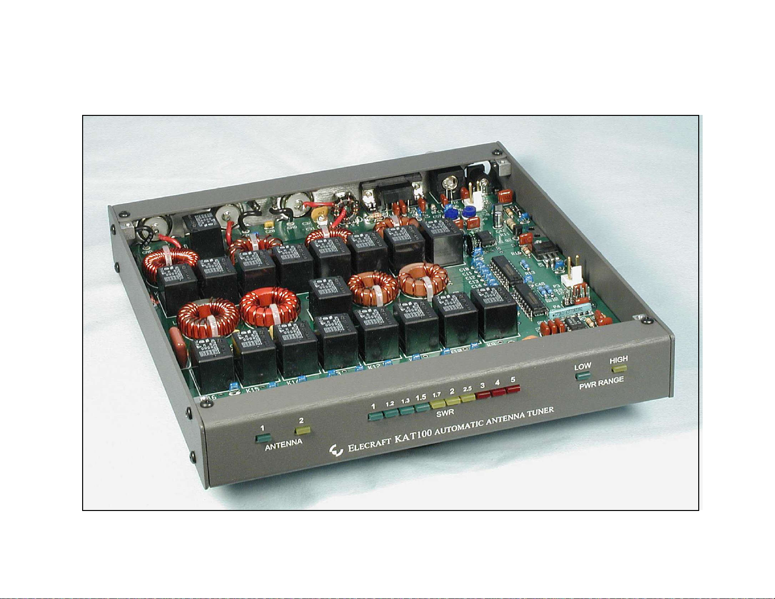
KAT100-1 shown above. See page 3 for photo of full-height version (KAT100-2).
1
Page 2

Table of Contents
Introduction ................................................................................................................................................................................................................3
Parts Inventory...........................................................................................................................................................................................................4
RF Board Assembly .................................................................................................................................................................................................8
Front Panel Board Assembly................................................................................................................................................................................18
Final Assembly........................................................................................................................................................................................................19
Alignment and Test ................................................................................................................................................................................................27
Using the KAT100...................................................................................................................................................................................................31
Troubleshooting......................................................................................................................................................................................................34
Specifications..........................................................................................................................................................................................................36
Circuit Details..........................................................................................................................................................................................................37
Schematic ............................................................................................................................................................................................. APPENDIX A
Parts Placement Drawing ..................................................................................................................................................................APPENDIX B
2
Page 3
Introduction
Tilt-Stand Options
The KAT100 automatic antenna tuner (ATU) is designed for use with
the Elecraft K2/100 transceiver, as well as the basic K2. It can match
loads with SWRs in excess of 10:1, and can easily handle 150 watts of
transmit power. Ten front-panel LEDs provide an accurate, real-time
SWR indication during transmit. The KAT100 also includes two
antenna jacks–the equivalent of two auto-tuners connected to the rig.
Because of its tight integration with the K2, the KAT100 offers many
advantages over generic external auto-tuners:
• Automatic power reduction to 2 or 20 watts (in low- and high-
power modes) when the K2's
possible with as little as 0.2 watts in low-power mode
• Direct display of power, SWR, and other data on the K2 LCD
• ATU can be configured using the K2 menu
• K2's POWER control setting indicated by two LEDs
• K2's
• L/C settings stored in EEPROM for both antennas on all bands
• SWR LEDs can use bar or dot mode (set by G R P H menu entry)
• All LEDs have two brightness levels (set by L C D menu entry)
The ATU comes in two enclosure styles, both of which match the K2:
A N T 1 / 2 switch selection indicated by two LEDs
T U N E switch is pressed; auto-tune is
Two different matching tilt stands are available, one for each KAT100
type. The E T S 2 is our standard, full-height tilt stand (2.5"), and is
recommended for use with the KAT100-2. The E T S 1 5 is identical to
the ETS2 but is only 1.5" tall. It's ideal for use with the low-profile
KAT100-1, providing the optimum viewing angle during operation.
Pre-Wound Toroids Available
The toroids in the KAT100 kit are not difficult to wind, and detailed
instructions are provided (beginning on page 13).
If you prefer not to wind the toroids yourself, you can obtain a full set
of pre-wound toroids (with leads stripped and tinned) from an Elecraftqualified source. Ordering information is at www.elecraft.com.
You do not need to send your cores or wire to the winding service. You
can keep your set for replacements or for use in your own projects.
• The KAT100-1, shown on the cover of this manual, is housed in a
low-profile cabinet, intended to be placed beneath the K2. Two
anti-slip brackets are provided, so the K2 will remain in position
even if the KAT100-1 is tilted up. (Also see Tilt-Stand Options
at right).
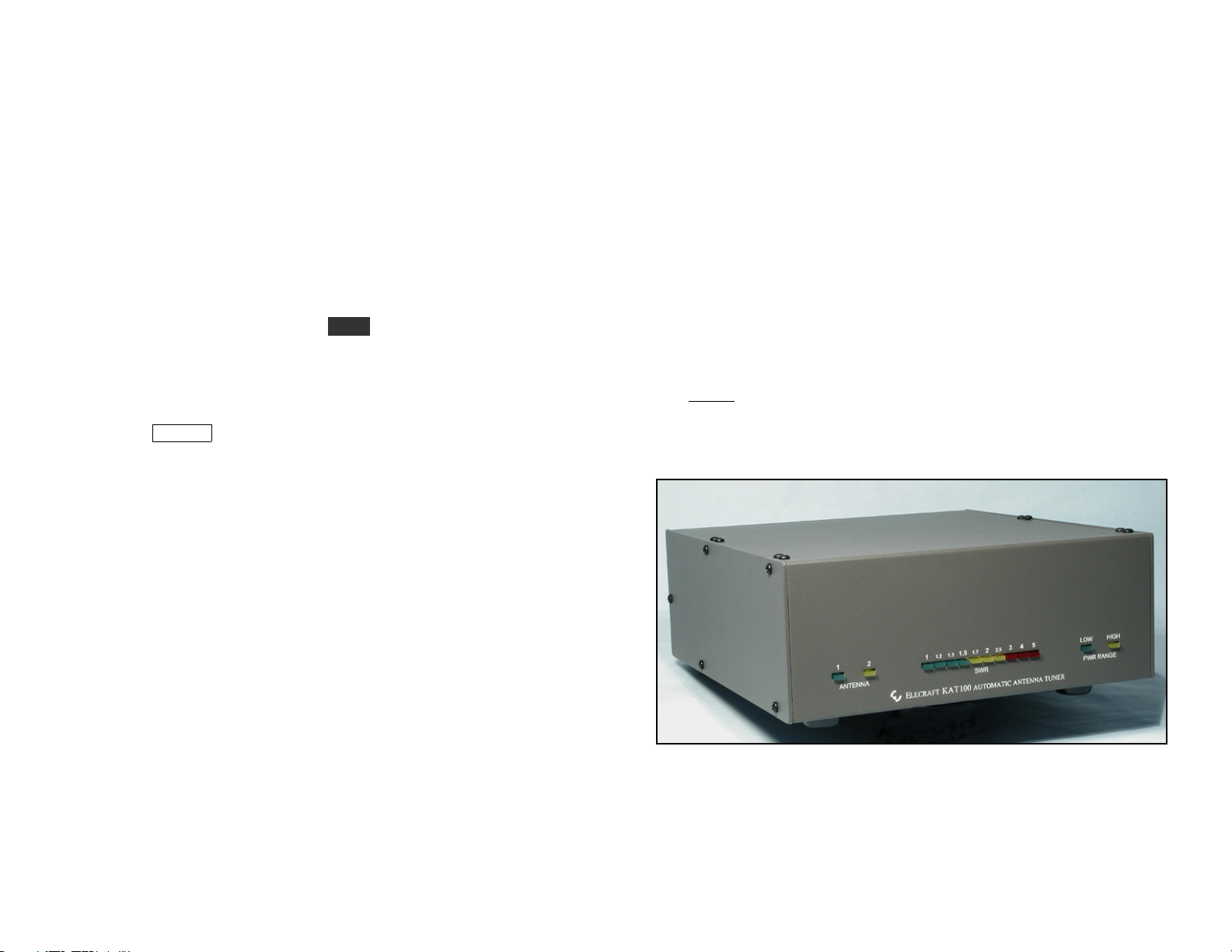
• The KAT100-2, shown in the photo at right, is intended for side-
by-side arrangement with the K2. It includes front and rear panels
that match our K2-sized EC2 enclosure kit. (The EC2 is sold
separately.) The EC2 cabinet provides plenty of room in the top
cover for your own accessories.
Both KAT100 types are covered in this manual.
KAT100-2
3
Page 4
Parts Inventory
You should do a complete inventory, and if you find anything missing, contact Elecraft.
i
Leave painted panels wrapped until they are needed during assembly. This will protect the finish.
Items supplied only with the KAT100-1 (with low-profile enclosure).
Picture Ref. Designator(s) QTY Description Part #
MISC 1 KAT100-1 Front Panel E100138
MISC 1 KAT100-1 Rear Panel E100139
MISC 2 KAT100-1 Side Panel E100140
MISC 1 KAT100-1 Top Cover E100146
MISC 1 KAT100-1 Bottom Cover (note: includes holes for optional feet/tilt-stand) E100147
The items below are in a small bag labeled "Misc., KAT100-1" (p/n E850132)
HDWR 28 Screw, 4-40 x 3/16" Panhead Phillips, black (includes several spares) E700015
HDWR 8 2-D Fastener E100078
MISC 4 Rubber foot, self-adhesive E700024
MISC 2 Anti-slide bracket E100150
Items supplied only with the KAT100-2 (for use with an EC2 enclosure).
Picture Ref. Designator(s) QTY Description Part #
MISC 1 KAT100-2 Front Panel, EC2-compatible E100142
MISC 1 KAT100-2 Rear Panel, EC2-compatible E100143
The items below are in a small bag labeled "Misc., KAT100-2" (p/n E850136)
P3, P6 2 Connector, 2 pin male, 0.156"spacing (Aux 12V In and Aux RF Out) E620012
P 4 1 Connector, 10 pin (5x2) male, 0.1" spacing (Aux Control) E620040
4
Page 5
Items in the KAT100 main parts bag (E850094), supplied with both KAT100-1 and -2. Color codes and markings are shown in parentheses.
Reference designators from 101 up refer to Front Panel components. Refer to Appendix A of the K2 owner's manual for more parts photos.
i
Some components in this kit can be damaged by static discharge. Before handling diodes, transistors, and ICs, touch a
grounded, unpainted metal surface, or use a wrist strap grounded through a 1 megohm resistor.
Picture Ref. Designator(s) QTY Description Part #
C1 1 Capacitor, 12 pF, 2000V ceramic (3 KV caps may be substituted for any 2KV)E530107
C2 1 Capacitor, 22 pF 2000V ceramic E530108
C3 1 Capacitor, 39 pF 2000V ceramic E530109
C4 1 Capacitor, 82 pF 2000V ceramic E530110
C5,C6A,C6B,C7A-7D 7 Capacitor, 150 pF 2000V ceramic ("151") E530111
C8 1 Capacitor, 1200 pF, 1600V polypropylene film ("122") E530112
C32 1 Capacitor, 100 pF, 200V ("101") E530034
C33-36,C47 5 Capacitor, .001 µF, 50 V ("102") E530001
C37,C38,C39,C45,
C46 C50,C51,
C44,C49,C101,C102,
C56
C9-30,C40,C41,C43,
C48,C52-55,C57-60
C42 1 Capacitor, 10 µF, 35 V electrolytic E530045
C31 1 Capacitor, 5-30 pF trimmer E540001
D1,D2 2 Diode, 1N5711 (small glass body) E560004
D3,D4 2 Diode, 1N5817 (large black body) E560008
D110,D111,D112 3 Rectangular LED, Red (long lead is anode -- see text) E570007
D101,D103,D104,
D105,D106,D113
D102,D107,D108,
D109,D114
E1 1 Screw terminal, right-angle PCB mount E700012
7 Capacitor, .01 µF, 50 V ("103") E530009
5 Capacitor, .047 µF, 50V ("473") E530025
34 Capacitor, 0.1 µF, 50V ("104") E530020
6 Rectangular LED, Green E570008
5 Rectangular LED, Yellow E570009
5
Page 6

J1 1 Connector, DC barrel jack, 2.1mm, right-angle PCB mount E620026
J2 1 Connector, BNC, right-angle PCB mount, with finishing nut and washer E850134
J3 1 Connector, DB9-F (female), right-angle PCB mount E620058
J4,J5,J6 3 Connector, SO239 E620064
J7 0 Connector, 6-pin female, 0.1" (not supplied; for future use) N/A
J101 1 Connector, 12-pin female, 0.1" spacing, PCB mount E620008
K1-K18 18 Relay, SPDT, 10A rating E640012
L1,L2,L3,L4 4 Toroidal inductor on T80-0 core (brown, 0.8" dia.); see text E680020
L5,L6,L7,L8 4 Toroidal inductor on T94-2 core (red, 0.94" dia.); see text E680018
P1,P2 0 Connector, 2 pin male, 0.1" spacing (not supplied; for future use) N/A
P 5 1 Connector, 12 pin male, 0.1" spacing, right-angle mount E620065
Q1 1 Transistor, PNP, modified TO-92 package, Zetex ZTX789A
Note: Q1's labeling may be hard to read. The part number should be marked
on the silver-colored side.
Q2,Q3 2 Transistor, MOSFET, TO-92 package, 2N7000 E580002
Q101,Q102 2 Transistor, NPN, TO-92 package, PN2222 E580001
R5,R101-R114 15 Resistor, 120 ohms, 1/4W, 5% (brn-red-brn) E500022
R2 1 Resistor, 200 ohms, 1W, 5% (red-blk-brn) E500074
R115 1 Resistor, 220 ohms, 1/4W, 5% (red-red-brn) E500002
R116 1 Resistor, 470 ohms, 1/4W, 5% (yel-vio-brn) E500003
R11 1 Resistor, 680 ohm, 1/2 W, 5% (blue-gray-brn) E500085
K2 CTRL-R12 1 Resistor, 820 ohm, 14 W, 5% (gray-red-brn) E500001
R1,R8,R9 3 Resistor, 3.3K, 1/4W, 5% (org-org-red) E500017
R12,R16,R17,R18 4 Resistor, 10K, 1/4W, 5% (brn-blk-org) E500015
R3,R4 2 Potentiometer, 100K trimmer ("104") E520001
R6,R7,R13 3 Resistor, 8.45K, 1/4W, 1% (gray-yel-grn-brn) E500071
R15 0 Resistor (not supplied; for future use) N/A
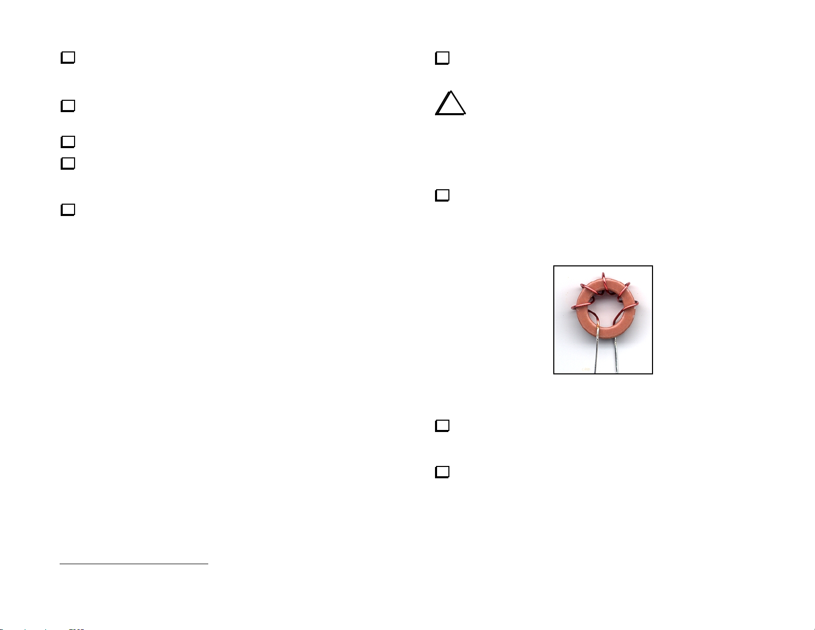
RFC1 1 RF choke, 15µH (brn-grn-blk) NOTE: may be in bag with toroid cores E690012
RFC2 1 Toroidal inductor on FT37-43 core (gray, 0.37" dia.); see text E680003
RP1 1 Resistor pack, 3.9K, 4 individual resistors, 8 pins E510000
T 1 1 Transformer on FT50-43 toroidal core; see text E680008
U1 1 IC, Programmed microcontroller for KAT100, PIC16F877 or PIC16F877A E610012
U2,U3,U4,
U101,U102
U5 1 IC, op-amp, LM358 E600010
U6 1 IC, high-current op-amp, EL5146C E600041
U7 0 IC, EEPROM, 25LC320 (not supplied; reserved for future use) E600009
U8 1 IC, 5V regulator, TO-220 package, 78M05 or 7805 E600024
W1-W7 0 Wire jumper (leave open except as specified in text) N/A
Z1 1 Ceramic resonator, 4.0MHz, 0.2% tolerance (orange, with 3 leads) E660001
5 IC, octal driver, TPIC6B595 E600032
E580019
6
Page 7
HDWR 2 L-bracket, front panel retainer, 4-40 threaded E700073
HDWR 14 Screw, 4-40 x 3/16" Panhead Phil, black (2 spares) E700015
HDWR 15 Screw, 4-40 x 5/16" Panhead Phil, zinc plated (2 spares) E700077
HDWR 1 Thumb screw, 6-32 x 1/2", with black plastic knob E700070
HDWR 1 Nut, 6-32 E700069
HDWR 2 Flat washer, #6 E700067
HDWR 24 Split lock washer, #4 (2 spares) E700004
HDWR 15 Nut, 4-40 (2 spares) E700011
HDWR 3 Solder lug E700062
HDWR 2 Standoff, hex male-female (for DB9 connector, J3) E700078
MISC 1 Connector, 2.1 mm mating plug for J1 (DC barrel jack) E620032
MISC 1 Connector, 9-pin, DB9M (male), solder cup terminals (for control cable) E620049
MISC 3 ft. Cable, 4-conductor shielded E760009
MISC 1 DB9 backshell and hardware (for control cable) E620050
MISC 1 40-pin socket for U1 E620017
MISC 1 ft. Hookup wire, #20, black insulation E760006
MISC 1 ft. Hookup wire, #20, red insulation E760007
MISC 4 ft. #26 enamel wire for T1 and RFC2, red E760002
MISC 2 ft. #26 enamel wire for T1, green E760004
MISC 20 ft. #20 enamel wire for L1-L8, red E760022
MISC 1 0 Cable ties (for L1-L8; 2 spares) E980002
MISC 1 Sand paper E850090
MISC 1 KAT100 RF PC Board E100144
MISC 1 KAT100 Front Panel PC Board (may be wrapped with one of the panels) E100145
7
Page 8
RF Board Assembly
Place the KAT100 RF PC board in front of you, with the bottom
side up and the front edge facing you as shown in the Parts
Placement Drawing, Appendix B.
On the bottom of the board, along both edges, you'll find six
locations for 2-D fasteners. These are used to secure the RF board to
the chassis panels. In the next few steps, just four 2-D fasteners will be
attached, and the remaining two locations will not be used. Which four
locations to use depends on whether you're building a KAT100-1 or
KAT100-2:
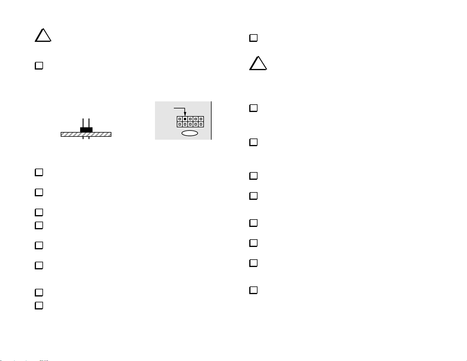
Install 2-D fasteners at the four locations identified earlier, on the
bottom of the RF board. Secure each fastener from the top side of the
board with 3/16" (4.8 mm) pan-head screws (black) and #4 split lock
washers (Figure 1b).
Make sure the 2-D fasteners line up with the edges of the PC
board and do not hang over. If they hang over or do not match their
component outlines, they are installed backwards.
i
The leads on small capacitors are fragile. Do not pull on
the leads or bend them excessively.
KAT100-1: Use the two 2-D locations near the front edge, and the
two near the back edge.
KAT100-2: Use the two 2-D locations near the front edge, and the
two located about two-thirds of the way back. (The 2-D fasteners are
supplied with the EC2 enclosure kit, not the KAT100-2.)
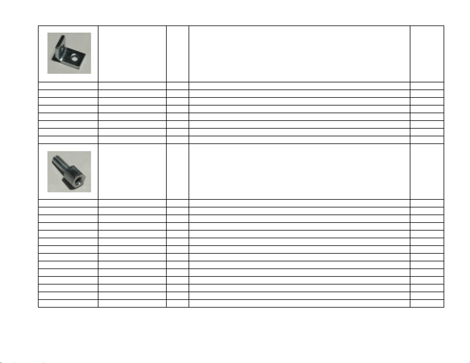
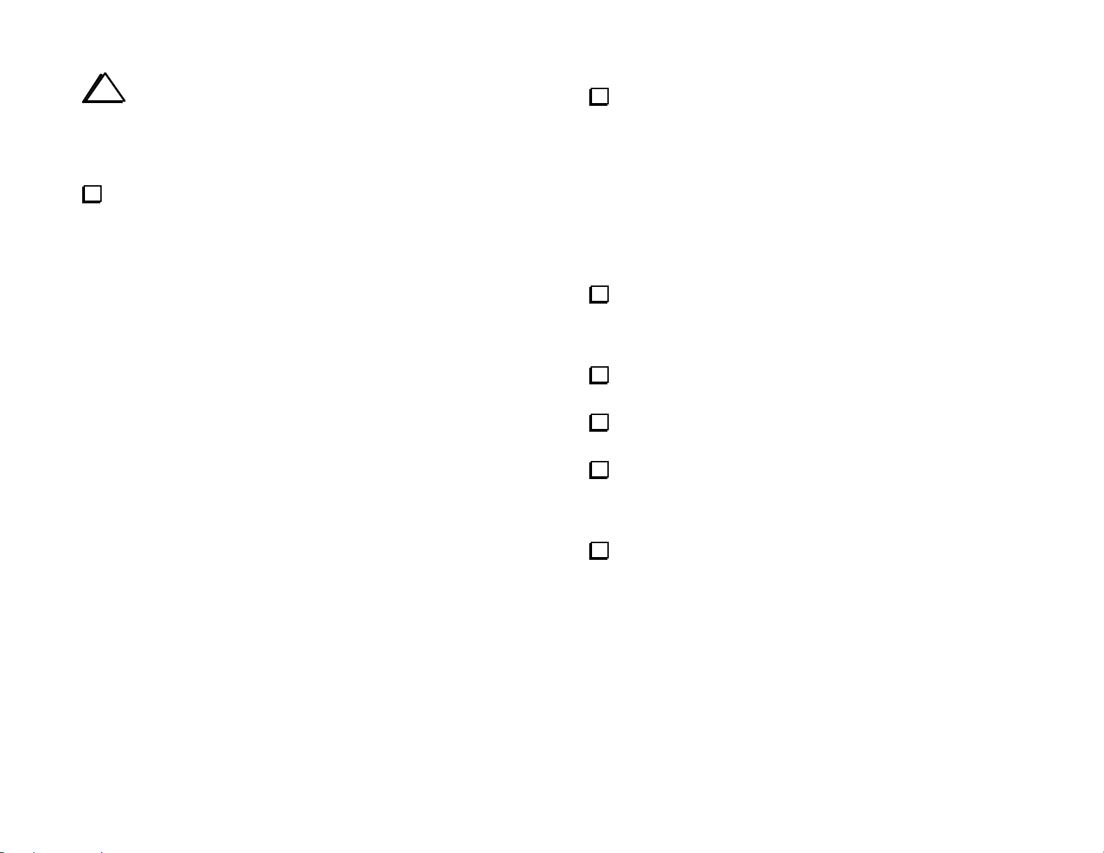
Locate a 2-D fastener and hold it vertically (Figure 1a). Looking
at a side with two holes, note that the holes are offset from the center.
The PC board outlines for the 2-D fasteners have a matching offset,
which will aid in installing them in the next step.
Holes offset
from center
(a)
Figure 1
(b)
Sort all capacitors into groups by physical appearance (size, color,
and lead spacing). Within these groups, sort them by capacitance
value.
Locate the component outline for capacitor C55, on the top side
of the board near the front edge.
Install a 0.1-µF capacitor (labeled "104") at C55. Keep the lead
length as short as possible. (If the leads are pre-formed, the capacitor
may sit slightly above the board.)
Bend C55's leads outward on the opposite side of the board to
keep it from falling out or shifting position. Then solder the capacitor
and trim the leads.
Note: Components may be soldered one at a time or in groups. Leads
can be trimmed either before or after soldering. After soldering, trim
leads to about 1/16" [1.5 mm] or less in length.
i
If your solder joints are not clean and shiny, your iron
may not be hot enough, or you may be using the wrong type of
solder. These "cold" solder joints will likely result in poor
performance, reliability problems, or component failure. You
may wish to consult our web site for additional soldering
instructions and tool recommendations.
8
Page 9
i
In the steps that follow, you'll be installing groups of
components. When working from a long list, install all of the items on
one line before moving on to the next. Arrows (⇒) appear in the list
to remind you of this order. In general, assembly proceeds from left to
right and front to back across the board.
Install the capacitors listed below. Start with C29, which is to the
left of C55, near relay K16. Check each capacitor's labeling
carefully (shown in parentheses).
Install the high-voltage capacitors listed below.
Note: Save a few of the clipped leads from these capacitors for use as
ground jumpers in later steps.
__ C1, 12 (12) ⇒ __ C2, 22 (22) ⇒ __ C3, 39 (39)
__ C4, 82 (82) __ C5, 150 (151) __ C6B, 150 (151)
__ C6A, 150 (151) __ C7D, 150 (151) __ C7C, 150 (151)
__ C7B, 150 (151) __ C7A, 150 (151)
__ C29, 0.1 (104) ⇒ __ C26, 0.1 (104) ⇒ __ C25, 0.1 (104)
__ C24, 0.1 (104) __ C23, 0.1 (104) __ C22, 0.1 (104)
__ C21, 0.1 (104) __ C20, 0.1 (104) __ C19, 0.1 (104)
__ C60, 0.1 (104)
__ C51, .01 (103) __ C50, .01 (103) __ C39, .01 (103)
__ C40, 0.1 (104) __ C38, .01 (103) __ C46, .01 (103)
__ C37, .01 (103) __ C48, 0.1 (104) __ C43, 0.1 (104)
__ C9, 0.1 (104) __ C18, 0.1 (104) __ C17, 0.1 (104)
__ C16, 0.1 (104) __ C15, 0.1 (104) __ C14, 0.1 (104)
__ C13, 0.1 (104) __ C12, 0.1 (104) __ C11, 0.1 (104)
__ C10, 0.1 (104) __ C52, 0.1 (104) __ C53, 0.1 (104)
__ C45, .01 (103) __ C54, 0.1 (104) __ C36, .001 (102)
__ C35, .001 (102) __ C41, 0.1 (104) __ C58, 0.1 (104)
__ C44, .047 (473) __ C49, .047 (473) __ C56, .047 (473)
__ C57, 0.1 (104) __ C47, .001 (102) __ C59, 0.1 (104)
__ C33, .001 (102) __ C34, .001 (102)
__ C32, 100 pF, 200V (101)
__ C28, 0.1 (104) __ C30, 0.1 (104)
__ C27, 0.1 (104) Near K17, middle of board
__ C8, 1200 pF (122)
Install the electrolytic capacitor, C42 (10 µF), near the back-right
corner of the board. The (+) lead must be installed in the hole marked
with a "+". The (+) lead is usually longer than the (–) lead, and the (–)
lead is identified by a black or white stripe.
Install the 5 to 30 pF ceramic trimmer capacitor, C31, near the
back edge of the board. Orient the flat side of the trimmer as indicated.
Using a small flat-blade screwdriver, set the trimmer to its
midpoint (screwdriver slot perpendicular to the flat side).
Sort all of the resistors by value. The color bands on 1% resistors
(which usually have a blue body) can be difficult to read, so you should
use a DMM (digital multimeter) to verify their values. Tape them to a
piece of paper with the values labeled.
Install the resistors below. Start with R18, which is at the front
edge of the board, near the microcontroller, U1 (the only 40-pin IC).
__ R18, 10k, 5% (brn-blk-org) ⇒ __ R17, 10K, 5% (brn-blk-org)
__ R5, 120, 5% (brn-red-brn) __ R9, 3.3k, 5% (org-org-red)
__ R8, 3.3k, 5% (org-org-red)
__ R7, __ R6, and __ R13, 8.45k, 1% (gray-yel-grn-brn)
__ R16, 10k, 5% (brn-blk-org)
__ R11, 680, 5% (blue-gray-brn), 1/2-watt
__ R12, 10k, 5% (brn-blk-org) __ R1, 3.3k, 5% (org-org-red)
9
Page 10
Install the 200-ohm, 1-watt resistor (red-blk-brn) at R2, on the
bottom of the board. Make sure R2 is flat against the board before
soldering.
Install diodes D1 and D2 (1N5711) near connector J3 at the back
edge of the board. Make sure the banded end of each diode is oriented
toward the right as indicated by its component outline.
Install resistor network RP1 (3.9k). RP1 is located on the right
side of the board, near relay K9. The dotted (pin 1) end of RP1 should
be oriented to the left. (RP1 is symmetrical and can be reversed, but
this orientation will help you visually identify the pin 1 end.)
Install trimmer potentiometers R3 and R4 (100 k, "104"), in the
back right corner of the board. The trimmers will sit a small distance
above the PC board on the pin shoulders.
Set both trimmer potentiometers to their midpoints.
i
The subminiature RF choke to be installed in the step has very
fragile leads. Do not pull on them. Keep soldering time to a maximum
of 2 seconds.
Locate the miniature 15-µH RF choke, RFC1 (brn-grn-blk), which
is the same bag as the toroidal cores. Install the choke in the backright corner of the board, near J3.
Check the resistance across RFC1 using the lowest resistance scale
of your DMM. This will ensure that the choke was not damaged during
soldering. The reading should be under 5 ohms.
Install the ceramic resonator, Z1, near the microcontroller. Z1
looks like a capacitor with three leads.
Near the "KAT100 RF" label in the front-left corner, you’ll find
a short jumper location, identified by a ground symbol (
discarded high-voltage capacitor lead to make a 3/4" (19 mm) U-
shaped wire for this jumper. Mount the jumper on the top side of the
board, with the top of the U-shape approx. 1/4" (6 mm) above the
board. Solder it from the bottom side.
). Use a
Install diodes D3 and D4 (1N5817), both located along the right
edge. Note that the banded ends of these diodes point in opposite
directions.
i
Before handling transistors in the next two steps, touch
an unpainted, grounded metal surface. Electrostatic discharge
can cause transistors to become damaged or intermittent.
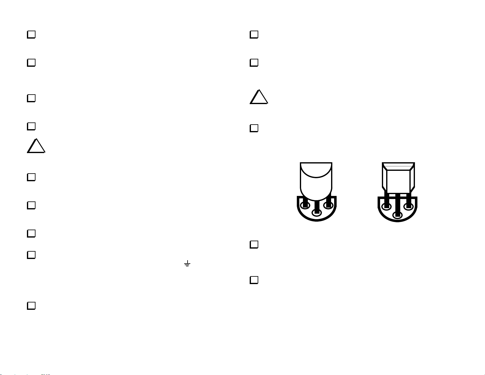
Using a magnifying glass if necessary, identify the three different
types of TO-92 package transistors (small black body, three leads).
They will look like one of the two types shown in Figure 2.
ZTX
(a)
Figure 2
Locate the two 2N7000 transistors. Install these at Q2 and Q3 as
shown in Figure 2a. Q2 is near the center 2-D fastener on the right
edge, and Q3 is near the microcontroller, U1. The flat side of each
transistor should be aligned with the flat side of its component outline.
Locate the ZTX789A transistor, which is labeled on its smaller
flat side. Install Q1, located near D4. Orient the transistor as shown in
Figure 2b.
(b)
789A
Install a similar jumper in the back-right corner, near relay K1.
10
Page 11
i
If you're building a KAT100-1, skip the remaining steps
in this column. Connectors P3, P4, and P6 are only supplied
with the KAT100-2 kit.
Install the 40-pin IC socket at U1. Orient the socket so the end
with the open notch is toward the right edge of the board.
Install the 10-pin, dual-row (5x2) male connector at P4, but do
not solder yet. Figure 3a shows P4 as viewed from right side of the
board. The plastic part of the connector must be on the top side of the
board, with the long end of the pins pointed up. The short ends are
inserted into the board.
Pin 4
P4
(a)
Solder just one pin of P4. Note: P4's plastic body can melt if too
much heat is applied. Limit soldering time to 2 to 3 seconds.
Examine P4 closely. If it is not flat against the board, re-heat the
soldered pin while pressing down on the plastic body of the connector.
Solder the remaining pins of P4. Do not trim the leads.
Cut pin 4 of P4 as indicated in Figure 3b, as close as possible to the
connector's plastic body.
(b)
Figure 3
P4
1
C46
i
In the following steps you'll be installing connectors at
the back edge of the PC board. These connectors must be
installed correctly in order for the rear panel to fit onto the
board. Figure 13 (page 20) shows how the rear-panel connectors will
appear once installed.
jack must be lined up with the slot-shaped holes in the component
outline. If the holes are a tight fit, press firmly until the connector
snaps into position, flat against the board. Solder all three pins.
Solder one of the large ground mounting pins first. If J2 then appears
to be tilted or twisted, reheat this ground pin while pushing J2 down
onto the board. Once it is seated properly, solder the remaining pins.
outline. Do not solder yet.
it is not flat against the board, re-heat the soldered pin while pressing
down on the connector. Then solder the remaining pins.
the entire hole).
Install the DC input jack, J1, at the back edge. The 3 leads on the
Install the AUX RF jack, J2 (BNC), in the back-right corner.
Install J3, the 9-pin "D" connector, as indicated by its component
Solder one of the 9 pins (near the center). Examine J3 closely. If
Solder J3's mounting tabs. Use a minimum of solder (do not fill
Locate a 2-pin, high-current male connector (0.156" lead spacing)
for use at P3.
Install P3 at its indicated location on the right side of the board,
but do not solder yet. Make sure the polarizing tab is oriented as
indicated by its component outline.
Press P3 down until it is flat against the board, then solder.
Install P6 (in the back-right corner) in the same manner as P3.
Locate screw terminal E1. If it was supplied with a screw, remove
it. The screw will not be used.
Place E1 in its indicated position, with the threaded hole facing
the rear edge of the board. Solder just one pin. CAUTION: This
part will get hot; don’t touch it with your finger while soldering.
If necessary, reheat the soldered pin of E1 and adjust it so that all
four pins are pressed down on the board as far as they'll go. Then
solder all pins.
11
Page 12
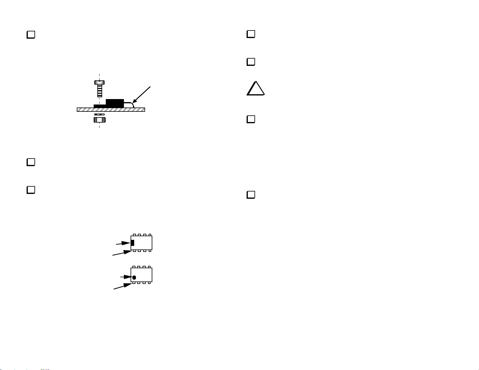
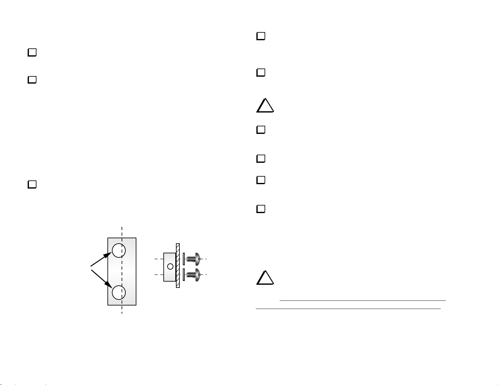
Locate voltage regulator U8 (78M05 or 7805). Bend the leads of
U8 to match its component outline (see Figure 4). Form the leads
around the shaft of a small screwdriver to create smooth rather than
sharp bends.
se smooth bend
Figure 4
Install U5 (LM358, 8 pins), which is located in the back-right
corner. A portion of the part number is printed on the board under the
IC ("358"). Do not solder yet.
Bend two opposite corner pins on the bottom side to hold the IC
in place. Solder all 8 pins (about 1 to 2 seconds per pin).
i
U2, 3, and 4 (TPIC6B595) are especially sensitive to
electrostatic discharge. Touch a grounded surface before
handling each of them.
Install the remaining ICs. Compare the part number on each IC to
the number printed on the board, and make sure that the pin 1 end is
oriented correctly.
__ U2, __ U3, and __ U4, TPIC6B595 (or similar number ending in "595")
Insert U8's leads into the proper holes. Secure U8 with a 4-40 x
5/16" (8 mm) machine screw (zinc plated, not black), #4 lock washer,
and 4-40 nut.
Solder all three leads. Trim the leads on the bottom side.
Note: The pin 1 end of ICs can be identified by a notch or dimple as
shown in Figure 5. This end must be oriented toward the notched end
of the component outline.
Notch
Pin 1
Dimple
Pin 1
Figure 5
__ U6, EL5146
Note: U7 is not used.
Remove the relays from their tube. If any of the pins are bent,
straighten them carefully using long-nose pliers.
12
Page 13
Place relays at locations K1-K18. The relays can only be installed
one way. Do not solder the relays yet, and do not clip or bend
the relay leads.
Sort the large toroidal cores into two groups: brown (T80-0, .80"
[20 mm]) and red (T94-2, 0.94" [24 mm]).
Using a thin hardcover book to hold the relays in place, flip the
PC board and book over together.
Solder just two diagonally opposite corner pins on each relay.
Turn the board back over. If any relay is not flat against the
board, re-heat its corner pins one a time while pressing down on the
relay.
Once all relays are properly seated, solder the remaining pins. Do
not trim relay leads, which can cause mechanical stress, reducing the
life of the relay.
Inductor Winding and Installation
A number of toroidal inductors are used on the RF board.1 The first
four inductors to be wound use type T80-0 cores. 80 specifies the
outside diameter in hundredths of an inch, in this case 0.80 inches
(20.3 mm). The -0 suffix refers to the core type, in this case
phenolic. In addition, four T94-2 cores are used (0.94", 24 mm). The
-2 refers to an iron powder core type.
There are also two ferrite toroidal cores used, one of type FT37-43
and one of type FT50-43. In this part number, FT identifies the core
as ferrite, and -43 identifies the type of ferrite. The number in the
middle again specifies the outside diameter. 37, the smaller size, is
0.37" (9.5mm). 50, the larger size, is 0.50" (12.7mm). Both ferrite
cores are dark gray in color and can only be differentiated based on
their size.
i
#20 enamel wire is quite stiff. After winding it tightly
onto the core, you may find that there's a small gap between
the wire and the core's flat surfaces. This will not affect
performance. If you try to wind the this wire so that it "hugs"
the core all the away around, you may have to pull the wire too
hard, resulting in hand fatigue.
(23 cm) of #20 red enamel wire. To wind L1, "sew" the long end of
the wire through the core. Each pass through the core counts as one
turn. Exactly 6 turns are needed, as shown in Figure 6. The enamel
insulation will be removed in a later step.
spacing is similar to that shown. If the spacing cannot be matched, it
may be because you have one turn too few or too many.
A T80-0 core (brown phenolic) will be used for L1. Cut 9 inches
Figure 6
Place L1 on top of its photo (Figure 6). Adjust the turns until the
Three types of enamel wire are supplied with the kit: #20 red, #26 red,
and #26 green. #20 wire is much larger in diameter than #26. Be sure
to use only the type called for in the instructions; do not substitute
other wire types. Cut wires to the specified lengths to avoid running
out of wire.
1
Pre-wound toroids are available from an Elecraft-approved source; see page 3.
Trim L1's leads to about 3/4" [19 mm] long as shown.
13
Page 14

i
In the next two steps, the leads of L1 will be stripped
and tinned. Toroid leads must be prepared correctly to
maintain reliability at the high voltages and currents seen by
the tuner.
There are three commonly-used methods to remove the enamel
coating from the leads: (1) heat-stripping, (2) burning/sanding, or (3)
scraping with a sharp tool. These methods are covered below.
(1) To heat-strip the enamel wire:
Secure L1 to the PC board using a cable tie. Two holes are
provided for this purpose, one inside the core and one outside. The
cable tie should be installed such that its "head" (thick end) ends up on
the bottom side, pressed tightly against the board (Figure 7).
• Place a small amount of solder (a "blob") on the end of your
soldering iron
• Insert the clipped end of the wire into the hot solder. If the iron is
hot enough, you should see the insulation bubble and begin to
vaporize after 4 to 6 seconds.
• Add more solder and feed more of the wire into it as the enamel
melts. Continue tinning the wire up to the edge of the core. Then
slowly pull the wire out of the solder.
• If any enamel remains on the lead, scrape it away using your
thumbnail or a sharp tool.
(2) The insulation can be burned off by heating it with a butane lighter
for a few seconds. Use sandpaper to remove the enamel residue.
(3) You can scrape the insulation off using a razor blade or other sharp
tool. Avoid nicking the wire.
Strip the leads of L1 as described above. Remove the enamel from
the leads up to the edge of the core (see Figure 6).
Tin L1's leads with fresh solder. If the solder on the leads looks
dull or is not adhering very well, remove any residual enamel and re-tin
the lead.
Install L1 flat on the board as shown by its component outline
near relays K1 and K2. Do not solder yet.
Figure 7
Using a ruler, make sure that the head of the cable tie does not
extend more than 0.25" (6 mm) below the bottom of the board. This
would prevent proper installation of the bottom cover.
Trim off excess cable tie length.
Solder the leads of L1. When soldering, make sure that the solder
binds well to the leads. If the lead appears to be an "island" in a
pool of solder, it is not making good contact; remove the toroid
and prepare the leads as described above. (For further
information, look for "Soldering Tips" on our web site.)
i
Do not apply adhesives or fixatives of any kind to toroids.
Using your DMM on a low resistance scale, check for continuity
between L1's pads (not the leads) on the bottom of the board. If the
reading is over 1 ohm, re-strip the leads. Note: Your DMM probes will
have some residual resistance. Short them together to measure this
amount, and subtract it from your continuity readings.
14
Page 15

Toroidal inductors L2-L8 are shown in the photos at right (Figure
8). Wind each of these toroids using the indicated cores, either T80-0
(brown, phenolic) or T94-2 (red, iron powder). All are wound using
#20 enamel wire. Use the wire length and number of turns shown.
Place each toroid on its photo and adjust the turns spacing so it is
similar to that shown. Re-check turns counts. (Recall that each pass
through the core counts as one turn.)
Prepare the leads of these toroids as you did for L1.
i
The T94-2 cores (red) have one side which is painted a darker
color than the rest of the core. To improve the appearance of the
completed RF board, we suggest mounting all four of these cores with
the dark side down.
Install L2-L8, using cable ties as you did for L1. Match each
toroid to its reference designator carefully. Exchanging any of them
will make tune up erratic and may prevent the ATU from finding a
match.
Note: Once in position, some of the toroids may be very close to each
other, and may even be touching. This will not affect performance.
__ L2: 10 T, T80-0 __ L3: 16 T, T80-0 __ L4: 23 T, T80-0
13" (33 cm) 19" (48 cm) 26" (66 cm)
__ L5, 12 T, T94-2 __ L6, 17 T, T94-2
18" (46 cm) 24" (61 cm)
Solder L2-L8.
On the bottom side of the board, check for continuity between
the pads of L2-L8. If you get a reading of over 1 ohm, remove the
toroid from the board and prepare the leads again.
__ L7, 24 T, T94-2 __ L8, 34 T, T94-2
34" (86 cm) 46" (117 cm)
Figure 8
15
Page 16

Locate the two dark gray (ferrite) toroid cores. The smaller of
(
)
(
)
the two (type FT37-43) has an outside diameter of 0.37" (9.5 mm).
This core will be used in the following steps.
RFC2 is wound on an FT37-43 core using 16 turns of #26 red
enamel wire (14", 36 cm). Wind and prepare this inductor in the same
manner as L1.
Install RFC2 vertically as indicated by its component outline near
relay K1.
i
Toroidal transformer T1 uses a bi-filar winding, which means
that two wires are wound on the core together. The wires will be
twisted together loosely before they're wound onto the core.
Cut two 11" (28 cm) lengths of #26 enamel wire, one red and
one green.
Twist the red and green wires together over their entire length.
The wires should cross over each other about every 1/2" (1 cm).
Wind 12 turns of the twisted wires onto the large ferrite core
(FT50-43). The turns should cover about 80-90% of the core, as
shown in Figure 9 (a white core was used to highlight the winding).
Strip and tin the leads of T1.
Using a magnifying glass, examine the red/green lead pairs to
make sure that the leads are not shorting together.
4
(RED)
2
GRN
Figure 10
3
(RED)
1
GRN
Separate T1’s leads as shown in Figure 10. The numbers on the
leads correspond to numbered pads on T1's PC board outline.
Figure 9
Install T1 vertically on the PC board as indicated by its outline
near the back edge of the board. Insert the red and green leads into
their numbered holes (see lead numbering above).
Verify continuity between the #1 and #4 pads of T1.
16
Page 17

Uninstalled Components
Resistance Checks
Verify that these locations on the RF board are not filled:
Top side:
__ U1 (microcontroller, 16F877), should not be installed in its socket yet.
__ U7, front edge
__ W1-W6, front edge
__ W7, back edge
__ J7, right front corner
__ P7, right side, near L2
Top side, KAT100-1 only:
__ P6, __ P3, __ P4 (all along the right edge)
Bottom side:
__ R15 __ P1 __ P2 __ P5
P5 will be installed in the next section. The other uninstalled
components are reserved for future use.
Visual Inspection
i
Nearly all problems with kits are caused by poorly-
soldered component leads or incorrectly-installed components.
You can locate and correct most assembly errors ahead of time
with a simple visual inspection.
closely for all of the following: cold solder joints (dull rather than
shiny appearance), solder bridges, and leads that are not soldered. Reheat any suspect joints.
re-check the orientation of all __ Diodes, __ Transistors, __ ICs.
Using a magnifying glass, examine the bottom of the PC board
Using the parts placement drawing at the end of the appendix,
Make the resistance measurements listed below, touching the
DMM's (+) and (-) leads to the indicated points. The schematic may be
helpful in troubleshooting any incorrect readings.
i
The symbol > means greater than. Your DMM may indicate
infinite resistance (all digits flashing) for readings in the table that
include this symbol. Other readings should be +/- 10 %.
KAT100 Test Points (+, -) Resistance
Between pins 2 and 5 of relays K1-K18
(on bottom of board, marked)
U8 (voltage regulator) "12V" pin, ground 1-30 k
U8 (voltage regulator) "5V" pin, ground 1-30 k
U2 (6B595) pin 2, ground 1-30 k
U2 (6B595) pin 3, ground > 100 k
U2 (6B595) pin 9, ground < 2 ohms
U2 (6B595) pin 12, ground > 100 k
U2 (6B595) pin 13, ground > 100 k
U2 (6B595) pin 18, ground > 1 k
U6 (EL5146) pin 2, ground 1-30 k
U6 (EL5146) pin 3, ground > 1 k
U6 (EL5146) pin 6, ground > 1 k
U6 (EL5146) pin 7, ground 1-30 k
U6 (EL5146) pin 8, ground > 100 k
U5 (LM358) pin 1, ground > 100 k
U5 (LM358) pin 2, ground > 100 k
U5 (LM358) pin 3, ground 45-55 k
U5 (LM358) pin 5, ground 45-55 k
U5 (LM358) pin 6, ground > 100 k
U5 (LM358) pin 7, ground > 100 k
D3 (1N5817) cathode2, ground > 100 k
D3 (1N5817) anode, ground > 100 k
D4 (1N5817) cathode, ground > 100 k
D4 (1N5817) anode, ground > 100 k
380-450 ohms
2
The banded end is the cathode.
17
Page 18

Front Panel Board Assembly
Place the Front Panel PC board in front of you with the
"KAT100 FP" label at the left.
i
Follow all LED installation instructions carefully to
preserve the appearance of your KAT100's front panel.
Sort the rectangular LEDs into groups according to color.
Install the following two resistors at the right edge:
__ R115, 220, 5% (red-red-brn)
__ R116, 470, 5% (yel-vio-brn)
Install 120-ohm resistors in all remaining resistor locations (R101
through R114).
Install the following components on the bottom side of the board:
__ Q101 and __ Q102, PN2222A (align flat side as indicated)
__ C101 and __ C102, .047 (473)
i
TPIC6B595 ICs are very sensitive to static discharge.
Touch a grounded, unpainted metal surface before handling
them.
pin 1 location. The labeling on U101 should read upside-down with
respect to the "KAT100 FP" label.
corner pins on the IC outward to hold it in place. The front panel
metal piece will not fit correctly unless U101 is seated flat on
the board.
Place a TPIC6B595 IC at U101, but do not solder yet. Note the
While holding U101 firmly against the PC board, bend the four
Re-check the orientation of U101, then solder.
Install U102 in a similar fashion.
Install a green LED at D101, at the left end of the Front Panel
board, but do not solder yet. As indicated on the board, the long
lead (anode) goes to the right.
Hold the LED flat against the board (not tilted). Bend the leads
outward on the bottom side to hold it in place. Then trim both leads.
Solder one lead of the LED, keeping soldering time to 1 to 2 sec.
If the LED is tilted or is not pressed flat against the board, re-heat
the lead while pressing the LED down.
Once the LED is correctly positioned, solder the other lead, again
keeping soldering time to 1-2 seconds.
Install a yellow LED at D102. Make sure the long lead is to
the right. Before soldering, adjust the LED's position as with D101.
Install green LEDs at D103, D104, D105, and D106. Make sure
the long lead is to the right for these and all remaining LEDs.
Install yellow LEDs at D107, D108, and D109.
Install red LEDs at D110, D111, and D112.
Install a green LED at D113.
Install a yellow LED at D114.
Using a discarded component lead, make a 3/4" (19 mm) U-
shaped wire for the ground jumper (
with the top of the U-shape no more than 1/8" (3 mm) above the
board. Solder from the bottom side.
), near R101. Mount the jumper
18
Trim all leads as short as possible on both sides of the board.
Page 19

Final Assembly
Straighten the leads of microcontroller IC U1 (PIC16F877) as
shown below. The rows of pins must be straight and parallel to each
other to establish the proper pin spacing. To straighten the pins, rest
one row of pins against a hard, flat surface. Press down gently on the
other row of pins and rock the IC forward to bend the pins into
position as shown below.
Flared
Straight
Figure 11
Insert U1 into its socket, with the notched or dimpled end of the
IC aligned with the notched end of its socket and outline. (The labeling
on the IC should be upside down with respect to the "KAT100 RF"
label at the left side of the board.)
Examine U1 closely. If any pins are bent, remove the IC and
straighten them. (To remove U1 from its socket, pry it up gently on
each end using a small flat-blade screwdriver.)
i
The right side view at Figure 12 shows how the Front
Panel and RF boards will be joined in the following steps.
J101 is a 12-pin female connector on the Front Panel board. P5 is a
12-pin right-angle male connector on the RF board. Also shown is one
of two L-brackets that secure the assembly and keep the Front Panel
board in a vertical position.
Place an L-bracket at one of the indicated locations at the front
edge the RF board. Align it with the component outline. If it's not
flush with the front edge, the short and long sides may be reversed.
Secure the L-bracket loosely to the RF board using a 4-40 x 3/16"
[4.7 mm] screw (black) and #4 lock washer.
Install the second L-bracket in the same way.
Top of RF board
101
Figure 12
Slide the 12-pin female connector (J101) onto the pins of the 12pin male connector (P5). There should be no gap between them.
Locate P5's outline on the bottom of the RF board. Insert P5's
right-angle pins into their holes. Do not solder yet.
Position the Front Panel board as shown above. The pins of J101
should be inserted into their holes, and the two L-brackets should be
aligned with their outlines on the back of the Front Panel board.
Secure the L-brackets loosely to the Front Panel using two 4-40 x
3/16" [4.7 mm] screws (black) and two #4 lock washers.
If the Front Panel is not aligned with the RF board along its front
edge, adjust the L-brackets positions.
P5
Locate the two small L-brackets. Identify the shorter side of the
"L", which will be attached to the RF board.
19
Tighten the all four L-bracket screws.
Solder all pins of J101 and P5.
Page 20

J6
Unwrap the rear panel piece, and place it with the labeling facing
away from you. Review Figure 13, which shows the vertical portion of
the panel, along with all of the panel- and PCB-mounted connectors.
Do not attach the rear panel to the RF board at this time.
Using the supplied sandpaper or a sharp tool, scrape away any
residual paint from around the hole for the ground terminal, E1. Do
this on the inside surface of the rear panel.
J5
J4
Figure 13
E1
Position J5 and J4 on the rear panel in the same way as J6, with
the solder cups facing up.
Attach J5 and J4 to the rear panel using the same hardware. Note
the position of the solder lug on J5, which differs from J4 and J6.
Cut six lengths of #20 stranded hookup wire (vinyl insulated):
J3
J2
J1
Sand or scrape residual paint from around at least one mounting
hole for each of the three SO239 connectors (J4, J5, and J6). Again,
this should be done on the inside surface.
Position J6 on the rear panel as shown. The connector's flange
should be on the outside of the panel. The center pin's solder cup
should be facing up to facilitate soldering in a later step.
Secure J6 with four 4-40 x 5/16" (8 mm) pan head screws, #4 split
lock washers, and 4-40 nuts. A solder lug takes the place of one lock
washer at the indicated corner, closest to the top edge of the rear
panel. Do not overtighten the hardware.
__ three black, 1.25" (3.2 cm) long
__ two red, 1.5" (4 cm) long
__ one red, 2.5" (6.3 cm) long.
Remove 1/4" (6 mm) of insulation from each end of all six wires.
Twist the strands of each wire tightly. Tin the wires using a small
amount of solder.
20
Page 21

KAT100-1 Enclosure Assembly
i
The instructions on the next two pages apply only to the
KAT100-1 (tuner with low-profile enclosure). If you're building
a KAT100-2, turn to page 23.
Solder the three black wires to the lugs on J4-J6 (Figure 14).
Secure E1 (ground terminal) to the rear panel with the 6-32
thumbscrew, 6-32 nut, and two #6 flat washers (Figure 13). The nut
must be installed between the washers and thumb screw as shown to
ensure good electrical contact.
Secure J3 (9-pin D connector) to the rear panel using two malefemale standoffs (see Figure 13). Do not overtighten the standoffs,
as they can easily be stripped.
Solder the three red wires to the center terminals of J4-J6. The
longest of the three red wires should be soldered to J4 (RF IN).
Slide the rear panel assembly onto the back edge of the RF board.
The connectors mounted on the RF board (E1, J3, J2, and J1) should
line up with their holes. Do not secure the rear panel or
connectors yet.
Locate the three pads labeled GND at the back edge of the RF
board. Pull the rear panel assembly back a short distance from the
board so that these pads can be soldered from the bottom side of the
board.
Solder one end of each of the three black wires to each of the
GND pads. The black wires and the approximate locations of their
associated GND pads can be seen in Figure 14.
Trim excess lead length from the GND wires on the bottom of
the RF board.
Slide the rear panel assembly full into place. The connectors
mounted on the RF board should press up against the inside of the
panel.
Secure the rear panel to the bottom of the RF board at the 2-D
fasteners using two 4-40 x 3/16 [4.7 mm] screws (black).
Secure J2 (BNC) to the rear panel using the supplied finishing nut
and lock washer.
Pass the longest red wire, which is soldered to J4's center
terminal, through the center of toroidal transformer T1.
Solder one end of this wire to the pad labeled RF IN.
Solder one end of each of the two remaining red wires to the pads
labeled ANT1 and ANT2.
Trim excess lead length from the wires just soldered on the
bottom of the RF board.
J6
J4J5
K18
GND
ANT2
ANT1
GND GND
RF IN
T1
Note: If the holes on the bottom portion of the rear panel do not line
up with the holes in the 2-D fasteners, you may not have the rear
panel pressed all the way onto the RF board.
Figure 14
21
Page 22

Unwrap the front panel piece. Slide it over the LEDs on the
p
Front Panel board, then secure it to the 2-D fasteners on the bottom
of the RF board using two 4-40 x 3/16 [4.7 mm] screws (black).
Unwrap the side panels, and lay them on soft cloth with the
painted side down. The sides that are oversprayed (lightly painted)
should be facing up.
Sand or scrape away the overspray in the area of all four
mounting holes on both side panels. Be careful not to nick or sand too
close to the edge of the panel.
Place 2-D fasteners on the inside surface of the side panels at the
two locations shown in Figure 15. The panels are symmetrical, so
either edge can be considered the top.
Holes offset
away from
anel
Secure each 2-D fastener to the side panel using one 4-40 x 3/16"
[4.7 mm] screw (black). The fasteners must be oriented as shown
in the detail drawing, Figure 16.
Figure 15
Attach the side panels to 2-D fasteners already installed on the
RF board. Use one 4-40 x 3/16" [4.7 mm] screw (black) per fastener.
Secure the side panels to top surfaces of the front and rear panels.
Use one 4-40 x 3/16" [4.7 mm] screw (black) per fastener.
Figure 16
Unwrap the bottom cover piece, which can be distinguished from
the top cover by the presence of mounting holes for a tilt stand and
rubber feet. It is painted on both sides.
If you have purchased a tilt-stand kit for use with the KAT100,
install the stand and front/rear feet now, following the instructions
supplied. Otherwise, install the four self-adhesive, low-profile rubber
feet supplied with the KAT100-1. Position them near the corners of
the bottom cover.
Install the bottom cover. Secure it to the RF board in four places
using 4-40 x 3/16" [4.7 mm] screws (black).
i
Continue with K2 Firmware Installation on page 24.
22
Page 23

KAT100-2 Enclosure Assembly
i
The instructions on this page apply only to the
KAT100-2 (EC2 version of the ATU). If you're building a
KAT100-1, use the instructions starting on page 21.
labeled "GND" at the back edge of the RF board. The black wires and
the approximate locations of their GND pads can be seen in Figure 14
(page 21).
Solder one end of each of the three black wires to the three pads
Look carefully at the locations of the screws holding the feet in
place. If the screws are near any component pins on the bottom of the
RF board, clip the component pins. This may require temporary
loosening of the rear panel hardware.
Secure J3 (9-pin D connector) to the rear panel using two malefemale standoffs (see Figure 13). Do not overtighten the standoffs,
as they can easily be stripped.
Secure J2 (BNC) to the rear panel using the supplied finishing nut
and lock washer.
Solder one end of the longer red wire to the pad labeled RF IN.
Solder one end of each of the two remaining red wires to the pads
labeled ANT1 and ANT2.
Trim excess lead length from all of the #20 wires on the bottom
of the RF board.
The ETS2 tilt stand option for the EC2 enclosure includes two
large, round back feet for the enclosure. If you have an ETS2, install
these feet on the rear panel using the supplied hardware.
Slide the rear panel assembly onto the back edge of the RF board.
The connectors mounted on the RF board (E1, J3, J2, and J1) should
press up against the inside of the panel.
Secure the rear panel to the bottom of the RF board at the 2-D
fasteners using two 4-40 x 3/16 [4.7 mm] screws (black). Note: If the
holes on the bottom portion of the rear panel do not line up with the
holes in the 2-D fasteners, you may not have the rear panel pressed all
the way onto the RF board.
Secure E1 (ground terminal) to the rear panel with the 6-32
thumbscrew, 6-32 nut, and two #6 flat washers (Figure 13). The nut
must be installed between the washers and thumb screw as shown to
ensure good electrical contact.
Solder the three black wires to the solder lugs on J4-J6 as shown
in Figure 14.
Pass the long red wire that is soldered to the "RF IN" pad through
the center of toroidal transformer T1.
Solder the three red wires to the center terminals of J4-J6 as
shown.
Unwrap the front panel piece. Slide it over the LEDs on the
Front Panel board, then secure it to the 2-D fasteners on the bottom
of the RF board using two 4-40 x 3/16 [4.7 mm] screws (black). (These
screws were supplied with the EC2 enclosure kit.)
Attach the bottom cover and side panels that came with the
Elecraft EC2 project enclosure. (If you also have an ETS2 tilt stand,
attach that to the bottom cover first.) The EC2 kit provides the
needed hardware. The EC2 top cover will be installed later.
23
Page 24

K2 Firmware Installation
To use the KAT100, your K2 firmware must be revision
2.03d or later, and the IOC must be revision 1.07 or later.
To determine what revision you have, turn the K2 on while holding
any switch pressed. You'll see a display such as this: 2 . 0 3 d 1 . 0 7 .
The number on the left is the revision of the K2 main microcontroller
firmware, U6 on the K2 Control board. It includes a letter suffix which
may be either upper or lower case. The other number is the revision
for the I/O controller (IOC), U1 on the K2 RF board. Record both of
the numbers here: K2 _______ IOC _______.
If you determine from the above that your firmware must be
replaced, or if new firmware was supplied by Elecraft, complete the
remaining steps on this page. Otherwise, turn to page 25.
1. If you will be replacing your IOC, record all of your primary menu
settings. (If your old K2 firmware was revision 2.00 or later, also
record your secondary menu settings.) Next, use C A L F I L to
obtain and record all of your filter and BFO settings for all modes.
Finally, record the settings for C A L C U R , C A L S H I , and
C A L S L O . (C A L t P A is stored by the KPA100, not the K2.
Do not run C A L P L L at this time.)
2. Turn the K2 off and remove the top cover or KPA100 module.
3. Remove the two screws that hold the control board to the front
panel. Also remove the KAF2 if present. Remove the control
board using the long-handled Allen wrench (supplied with the K2).
4. Touch an unpainted, grounded metal surface. Remove the
old K2 firmware, U6 (Control board), using a small screwdriver to
pry it gently out of its socket at both ends. Store it in a safe place.
5. Straighten the leads of the new microcontroller (PIC18C452).
6. Install the new microcontroller. Orient the notched or dimpled end
of the IC with the notched end of its component outline.
7. Install R12 and remove C44 as described on page 26, right column.
8. Reinstall the Control board. Also reinstall the KAF2 if applicable.
9. If your I/O controller firmware is revision is 1.05 or earlier,
remove U1 on the RF board and install the replacement IOC here.
10. Turn on the K2. You may see I N F O 2 0 1 (for about 11 seconds) if
you have installed a new IOC.
11. If you saw I N F O 2 0 1 , you will need to re-enter all of your menu
and filter parameters (saved in step 1).
12. Test your sidetone using the S T L menu entry. If the sidetone is
missing,
change the sidetone source. The default is U 8 - 4 , compatible with
the KPA100 and KIO2.
13. If you have the K60XV option installed (60 meter adapter), set
the D 1 9 secondary menu entry to Y (see K60XV manual).
If you are upgrading from K2 Rev. 2.01 or earlier, you must
perform the VFO calibration steps below. This procedure is done only
on 40 meters. It does not have to be repeated on each band.
1. Allow the K2 to warm up at normal operating room
temperature for at least five minutes.
2. Plug the K2 frequency counter cable into P6 on the Control board.
Connect the probe end to test point TP1 on the RF board (VCO).
3. Switch to 40 meters and set the VFO to about 7100 kHz.
4. Tap M E N U
the parameter to P L L . Hold
procedure. You'll see a frequency in the 12 MHz range displayed,
and the letter "d " will flash as the firmware records calibration
data. After approximately 5-10 minutes, you'll hear a short tone,
and E N D will be displayed. Tap any switch to clear this message.
i
verify that you were on 40 m, with the counter cable at TP1.
5. You can check the VFO's accuracy using a signal at a known
frequency (see page 98 of the K2 manual). Note: In the Revision
C K2 manual, steps 8 and 11 on page 98 are incorrect for the new
firmware. C A L P L L is now run only once, and only on 40 m.
6. Move the K2 counter cable to the BFO test point, TP2 (or
remove the cable and store it).
7. Re-install the top cover or KPA100 module.
If you installed new firmware, read the K2 Revision 2 Firmware
manual to become familiar with any new features or changes.
E D I T the S T L parameter, then tap D I S P L A Y to
and locate the C A L entry. Hold E D I T , then change
E D I T again to begin the calibration
If you see I N F O 2 3 2 at any time during VFO calibration,
24
Page 25

KAT100
(MALE)
KAT100 CONTROL CABLE
K2 OR K2/100
(MALE)
OPTIONAL RS232 CABLE TO PC
(SEE K2/100 or KIO2 MANUAL)
PC
(FEMALE)
5
9
8
7
6
BLK
RED
WHT
GRN
BARE
1
BLK
RED
WHT
GRN
BARE
Control Cable Assembly
Locate the 4-conductor cable. Cut a 2' (60 cm) length. Note: A
shorter cable can be used as long as it accommodates the physical
orientation of the K2 and the ATU. A longer cable can also be used,
but it will have to be tested to ensure that it is not subject to RF
interference. A more heavily-shielded control cable may be required.
Remove 1/2" (12 mm) of the jacket from the cable at each end.
Be very careful not to nick the individual wires.
Peel back and cut away the foil shield.
Strip off 3/16" (5 mm) of insulation from each insulated wire.
Twist the strands of each wire together. Tin lightly with solder.
5
9
4
8
3
7
2
6
1
Figure 17
BLK
GRN
RED
BARE
BLK
GRN
RED
5
4
3
2
1
You should now have two DB9M (male) connectors: one that was
supplied with the KAT100, and one from the KIO2 or KPA100. (The
latter may already be part of an RS232 cable.) Orient the two male
connectors as shown in the left side of Figure 17. The solder cups
should be facing up, and the 4-pin rows should be to the left.
Clamp the left-most male connector into a padded vise, if
available.
Solder the BARE (shield), GREEN, WHITE, RED, and BLACK
wires to the indicated connector pins at the KAT100 end of the cable.
It may be helpful to melt some solder into each solder cup on the
connector first.
Remove the left male connector from the vise (KAT100 end),
and insert the other male connector (K2 or K2/100 end).
If you previously built an RS232 control cable for use with the
KPA100 or KIO2, remove the backshell from the K2 end. Orient the
cable as in Figure 17, with the PC end (female) to the right.
If you have not built an RS232 control cable, you should have an
unused DB9M (male) connector that was supplied with the KIO2 or
KPA100 kit. Locate this connector for use in the next step.
Solder the wires to this connector as shown. If there are RS232
interface wires already connected, you'll need to solder the bare wires
from both the KAT100 control cable and the RS232 cable to pin 1.
Remove the connector from the vise.
25
Page 26

Locate the connector housing (backshell) and associated hardware.
Note: A single hinged backshell may be provided rather than a twopiece backshell.
Attach a backshell to the male connector at the KAT100 end of
the cable. Figure 18 shows how the backshell appears when assembled.
Use the provided cable clamp to hold the cable in position, then secure
the clamp with two screws. The jackscrews must be retained by the
shells. Secure the backshell halves with the provided hardware (or, if
the shell is hinged, snap the backshell closed).
K2 Control Board, R12
If your K2 is s/n 2999 or lower, you'll need to install a resistor in series
with the VRFDET line on the K2 Control board as described below.
This will protect the K2's microcontroller from accidental damage if
you have a short in the KAT100 control cable. (K2s s/n 3000-up
already have this resistor, designated R12.)
Remove the two screws that hold the K2 control board to the
front panel. Also remove the KAF2 if present. Remove the control
board using the long-handled Allen wrench (supplied with the K2).
Locate the trace on the top side of the K2 Control board that
runs between resistors R8 and R9 (see drawing below). Cut the trace.
JACK SCREW
CLAMP
Figure 18
Attach a backshell to the connector at the K2 end. If you have
not built an RS232 cable, you should have an unused backshell from the
KIO2 or KPA100 kit. If you did build an RS232 cable, re-install the
backshell you removed earlier. The hole in the backshell should
accommodate both 4-conductor cables.
BACK SHELL
Power Cable Assembly
The KAT100 requires a source of 10-15 V DC. A mating plug is
supplied for the KAT100's power jack, J1. You can make a separate
cable for the KAT100, or build a "Y" cable to share power with the K2
or K2/100.
On the bottom of the board, solder an 820-ohm resistor (grayred-brown) between the two vias. You'll need to pre-trim the resistor's
leads since it isn't possible to cut the lead that falls between R8 and R9.
R8 R9
R12 (on back)
Cut
K2 Control Board, C44
Remove the Control board, if necessary (see above).
C44 (0.1 µF) on the K2 Control board, if present, must be
removed (it causes inaccuracy in current measurement). On the
revision B Control board, C44 is located near microcontroller U1. On
earlier Control boards, C44 is not on the board, but in lieu of this you
may have soldered a capacitor directly across R7. Remove it in either
case.
If your power supply does not have a fuse, you may wish to add a
1-amp fuse of any type in-line with the KAT100's DC input.
26
Page 27

Alignment and Test
Menu and Relay Test
Initial Tests
i
Do not transmit during these tests.
Turn the K2 and all power supplies OFF.
Reinstall the K2 Control board and KAF2 if not installed.
Connect the KAT100 to a source of 10-15 V DC (J1).
Connect the control cable between the KAT100 CONTROL
jack (J3) and the AUX I/O jack on the K2 or K2/100.
i
In the following steps, if you see or smell smoke, turn
off the K2 and all power supplies and refer to Troubleshooting.
The LEDs on the KAT100 should remain off and you should not
hear any relays switching yet.
cause the KAT100 to turn on as well. Only two KAT100 LEDs should
turn on: ANT1 or ANT2, and LOW or HIGH power. You may also
hear one or more relays switch.
the KAT100 antenna relay, K18. The ANT1 and ANT2 LEDs, as well
as the ANT2 annunciator on the K2, should agree.
If the KAT100 is powered from a separate supply, turn it on first.
Turn on the K2's power supply, then turn on the K2. This should
Tap the A N T 1 / 2 switch a few times. Each tap should activate
Tap M E N U , then use B A N D + / B A N D - or the VFO knob to
locate the A T U menu entry. Hold
the A T U parameter appears as two dashes (- - ), refer to
Troubleshooting.
Using the VFO knob, scroll through the A T U menu parameters.
You may hear relays turning on and off as you select various entries.
You should see C A L , A U T O , etc. Each menu entry will be explained
in the Using the KAT100 section.
Set the A T U parameter to L 0 . You should hear a relay switch
when you move from L 0 to L 1 , then to L 2 , etc., up through L 8 .
The same should be true for C 0 through C 8 , as well as N 1 and N 2 .
These menu selections can be used to identify failing relays or other
components. This is covered in the troubleshooting section.
Set the A T U parameter to C A L . Tap M E N U once to return to
menu scroll mode, and a second time to exit the menu.
Turn the K2 off and back on. Use the menu to verify that the
A T U parameter is still set to C A L , then exit the menu.
E D I T to modify the parameter. If
Preparing the KAT100 for Alignment
i
If you're planning to install any accessories of your
own in the top cover of the full-height KAT100-2, do not
connect them until after the KAT100 is aligned. Do not connect
anything to P3, P4, and P6 on the KAT100 RF board at this time.
Switch to a different band, and select the other antenna. Changing
back and forth between these two bands should now recall the selected
antennas. Turn power off and back on and verify that the appropriate
antenna is still selected for each band.
If you have a KPA100 installed, rotate the POWER pot through
its full range. The LOW power LED on the KAT100 should turn on
at 10 W and below. The HIGH power LED should turn on above
10 W.
Turn the K2 off.
Disconnect the KAT100's DC power cable. It must be left
disconnected during all alignment steps.
Disconnect the control cable between the KAT100 and the
transceiver. This cable must be left disconnected during all
alignment steps.
27
Page 28

i
During the first two parts of ATU alignment, the transmitted
signal will be fed through the ATU backwards from the normal
direction. That is, the transceiver will be connected to the KAT100's
ANT1 jack, and the dummy load will be connected to the KAT100's
RF IN jack. This provides a more accurate SWR bridge null, and will
also allow direct calibration of the REFL potentiometer (R4).
antenna jack on the K2 or K2/100. There are three possibilities:
• K2/100: use the SO239 jack on the back of the KPA100 module
•
•
Connect the KAT100's ANT1 jack (J5) to the appropriate
Basic (10-watt) K2 without a KAT2 (20-W ATU) installed: use the
K2's normal BNC antenna jack on the lower rear panel
Basic (10-watt) K2 with a KAT2 installed: use the KAT2's ANT1
jack on the upper rear panel
SWR Bridge Null Adjustment
Make sure the KAT100 is set up exactly as described on page 27
(Preparing the KAT100 for Alignment). The signal must be routed
backwards through the ATU, and the KAT100 DC and power cables
must be disconnected.
Locate a non-metallic tuning tool suitable for adjusting the SWR
bridge trimmer capacitor, C31.
You can use a DMM or an analog volt meter to null the SWR
bridge. Set the meter for 2 or 3 volts DC full-scale. Connect the (-)
lead to the ground jumper near the front of the KAT100 RF board.
Use an alligator clip so you won't have to hold the lead in place.
Touch the voltmeter's (+) lead to pin 3 of U5 (see Figure 19).
Note: There will be a DC voltage on this pin during transmit, even
though the KAT100 is not connected to a power supply.
Connect a 50-ohm dummy load to the KAT100's RF IN jack (J4)
using a short coax cable. The dummy load should have a rating of at
least 5 watts. If you have a K2/100, we recommend that you do all
alignment at higher power (20 watts) to improve calibration accuracy.
In this case you'll need a higher-wattage dummy load.
Turn on the K2, and switch to the 40-meter band.
If you have a KPA100 installed and a dummy load rated at 20
watts or higher, set the POWER control for 20 watts. Otherwise, set
the POWER control for 5 or 10 watts. Use 10 watts if your dummy
load can handle this level, at least for short transmissions.
Set the KAT100's FWD and REFL power potentiometers (R3 and
R4) to about the middle of their range.
in 5
in 3
Figure 19
Enter tune mode by holding
reading on the voltmeter (0 volts, or close to it). Hold
when finished.
i
You may see an indication near 0 volts over a small
range of C31's rotation. It is very important to position C31 in
the middle of this range. Repeat the null adjustment step until
you're sure that C31 is positioned correctly.
TUNE
. Adjust C31 for a minimum
TUNE
again
28
Page 29

Power Calibration (R3 and R4)
Make sure the KAT100 is set up exactly as described on page 27
(Preparing the KAT100 for Alignment). The signal must be routed
backwards through the ATU, and the KAT100 control and power
cables must be disconnected.
Power Calibration Voltage Table: During power calibration, a DC
voltage will be present at pin 3 or 5 of U5 (LM358) even though the
KAT100 is not connected to a power supply. The table below shows
target voltages at U5 corresponding to 5, 10, and 20 watts output. One
of these power levels will be used in the steps below.
Power Level Voltage at U5
5 W 1.3 V
10 W 1.8 V
20 W 2.7 V
Select one of the power levels indicated in the table above. If you
have a K2/100, 20 watts is recommened. Otherwise, use 10 watts (if
you have a 10 watt dummy load) or 5 watts. You will only need to do
calibration at one power level.
Disconnect the cables at the KAT100's RF IN and ANT1 jacks
and reverse them.
Touch the voltmeter's (+) lead to pin 3 of U5 (Figure 19).
Enter tune mode, overriding the power limit if applicable. Adjust
R3 (FWD) until the target voltage is reached. Hold
TUNE
to exit.
With power and control cables still disconnected from the
KAT100, measure the resistance from pin 5 of U5 to ground. Record
the value here: ______ k.
Multiply this amount by 1.2 (example: if the reading is 50 k,
multiplying by 1.2 yields 60 k). Your calculated value: _______ k.
Adjust R4 (REFL) until the resistance measured at pin 5 equals
your calculated value. (This step improves the accuracy of reflected
power and SWR measurements.)
Use a DMM for power calibration (20 or 30 V DC full-scale). The
(-) lead should be connected to a the KAT100's ground jumper.
Touch the DMM's (+) lead to pin 5 of U5 (see Figure 19).
Enter tune mode by holding
DMM reads close to the target voltage from the table. Hold
TUNE
. Adjust R4 (REFL) until the
TUNE
again when finished.
Note: In high-power mode, the power shown on the LCD should
stabilize near the desired level (20 watts) after a few seconds. On a
basic K2, power may drift upwards. Repeat the adjustment if needed.
29
Page 30

Top Cover Installation
Anti-Slide Brackets (KAT100-1 only)
Turn off the K2 and KAT100.
Unwrap the KAT100 top cover. Set it upside down on a soft
cloth to protect the finish. Note: The top cover is fabricated from
steel, not aluminum, to minimize interaction between the ATU and
the K2 when the two are stacked. Since it is steel, the top cover is
painted on both sides to protect against rust. Either side can be used as
the top surface.
Sand or scrape away the paint around all four mounting holes on
one side of the top cover.
Install the top cover using four 4-40 x 3/16" (4.7 mm) black
screws.
1
2
(detail
at right)
The KAT100-1 is designed to be placed beneath the K2. If the two are
then tilted, using the optional ETS15 tilt stand or a slanted operating
surface, the K2 tends to slide off during operation. To keep the K2 in
place, you can install the two supplied anti-slide brackets. The K2's
rear feet slip over the short standoffs on the brackets.
Identify rear-corner locations 1 and 2 on your top cover (Figure
20a).
Install an anti-slide bracket at location 2 using the two screws
already present at this location (see detail, Figure 20b).
Install the second anti-slide bracket at location 1. It should be
rotated 180 degrees in relation to the bracket at location 2.
(a) (b)
Figure 20
30
Page 31

Using the KAT100
GND (E1)
CAUTION: Never touch an exposed antenna wire when
transmitting. If you ever receive an RF burn, stray RF may be
the cause (see Antenna Considerations, page 33).
Rear Panel Connectors
12VDC (J1)
The KAT100 must be connected to a 10-15 V DC source. The
KAT100's power supply must be turned on first if it is separate
from the transceiver's power supply. Typical current drain is 200-
300 mA, but it can be as high as 700 mA in the unlikely event that all
relays and all LEDs are turned on simultaneously
AUX RF (J2)
This connector is not used by the KAT100 itself. It could be used for
RF signal routing to an accessory module built into the ATU.
J2 is connected internally to 2-pin male connector P6 via series
capacitor C49. P6 is supplied only with the KAT100-2. A mating
female connector may be purchased from Elecraft if required
(#E620013 housing, plus two #E620014 crimp pins).
CONTROL (J3)
3
.
A good ground should be connected to the KAT100. This is especially
important with high power (K2/100). See Antenna Considerations.
RF IN (J4)
J4 must be connected to the appropriate antenna jack on the K2 or
K2/100 via a short 50-ohm coaxial cable. There are three possibilities:
• K2/100: use the SO239 jack on the back of the KPA100 module
• Basic (10-watt) K2 without a KAT2 (20-W ATU) installed: use the
K2's normal BNC antenna jack on the lower rear panel
• Basic (10-watt) K2 with a KAT2 installed: use the KAT2's ANT1
jack on the upper rear panel
Note: If both a KAT100 and KAT2 are in the system, the KAT2 will
be switched to C A L P mode, and its ANT1 jack selected. The
A N T 1 / 2
switch and A T U menu entry will control only the KAT100.
ANT1 (J5) and ANT2 (J6)
Unbalanced antenna jacks (a balun is required with balanced feed lines).
The K2's
A N T 1 / 2
switch selects the antenna.
Front Panel LEDs
The KAT100 requires control signals from the transceiver's AUX I/O
port to operate. The AUX I/O port is included with the K2/100. In the
case of the K2, the KIO2 option is required.
Assembly instructions for the KAT100 control cable can be found on
page 25.
3
All relays and LEDs on. This is very unlikely to occur; in normal use, the
maximum will be closer to 400-500 mA. If you're concerned about current drain,
you can use the K2's G R P H menu entry to select D O T mode for the LED
bargraphs on both the K2 and the KAT100, or install KAT100 jumper W1 to
force DOT mode for just the KAT100 regardless of the G R P H menu setting.
ANTENNA (1 and 2): These indicate which antenna is selected. If
ANT 2 is selected, the K2's ANT2 LCD annunciator will be turned on.
SWR (1-5): SWR indication, 1:1 to 5:1 (or higher), during transmit.
POWER (LOW and HIGH): If the KPA100 is enabled and set for
over 10 W, the HIGH LED will turn on. Otherwise, LOW will be on.
Jumpers (W1-W7)
Installing W1 forces D O T mode for the SWR LEDs, regardless of the
K2's G R P H setting. W2 forces B A R mode. W3-W7 are not used.
31
Page 32

Normal ATU Operation (AUTO Mode)
(p
)
(p
)
(p
)
(p
)
Bypassing the Matching Network (CAL mode)
For normal operation, set the A T U menu entry to A U T O .
Hold
T U N E to start auto-tune. Power will be decreased to 2 W (basic
K2) or 20 W (K2/100) if set above these levels. Power and SWR will
be displayed on the LCD during tune-up (e.g. 2 0 1 . 5 - 1 ). The SWR
portion of the display may flash occasionally if you're using high
power. SWR will also be shown on the KAT100's SWR LEDs.
The ATU itself will terminate
T U N E after 1-5 seconds.
The ATU's L and C settings are stored in EEPROM, then recalled
instantly when you change bands or antennas. If you move
significantly off frequency, you may need to retune in order to keep
SWR low (especially at high power). The SWR LEDs on the KAT100
are activated during transmit to alert you to SWR changes.
Important ATU Operating Tips
• If the KAT100 uses a separate power supply from the
transceiver, the KAT100 supply must be turned on first.
• Erratic behavior of either the KAT100 or K2 may be observed
during auto-tune if excessive RF gets into the cables or circuitry. If
this happens at high power, reduce power to 10 watts or less for
auto-tune purposes. See Troubleshooting for other suggestions.
• Holding
(2 watts for a basic K2, 20 watts for the K2/100), and temporarily
suspends A U T O mode. This is useful when you want to check
power output with the present L and C settings.
• A very low SWR is not necessary for good antenna performance,
but it will allow operation of the K2/100 at maximum power
output (see Antenna Considerations).
• If you tap
T U N E , you'll see the K2's transmit-mode voltage and current drain,
not power output and SWR. The tune-mode power limit will be
overridden, and the ATU's L and C settings will not change.
• The ATU menu entry can display current values of L and C,
network type, and other data. See ATU Menu Settings at right.
• Sometimes a slightly lower SWR can be found by repeating
T U N E + D I S P L A Y overrides the tune-mode power limit
D I S P L A Y to show the voltage/current display, then hold
T U N E .
You can bypass the matching network by setting the A T U menu entry
to C A L . This sets the L and C values in the matching network to
zero. However, there will still be considerable stray reactance present
within the ATU. This stray reactance may de-tune any antenna or
dummy load connected to the ATU's antenna jacks.
As an alternative to C A L , you can tune up the ATU into a 50-ohm
dummy load on each band using A U T O mode. This will cancel out the
tuner's stray reactance. After tuning up on all bands, put the ATU into
SWR (x . x - 1 ) mode, which will preserve the L and C settings.
ATU Menu Settings
The table below lists all settings for the A T U menu entry. A U T O
mode is used most of the time. In this mode the ATU terminates
T U N E automatically. The other modes are primarily used for
calibration and test. When you switch between C A L and A U T O
mode, you may hear a few relays switching, since in C A L mode, L and
C are set to 0. You'll also hear relays switch if you select the L 0 - L 8 ,
C 0 - C 8 , or N 1 - N 2 modes (see Troubleshooting).
Mode Description Mode Description
C A L Bypass (L/C = 0) E x x x 0-199 = error code;
see Troubleshooting
A U T O Auto-tune mode I N I T Resets all L/C to 0 on
next power-up
x . x - 1 Auto-tune SWR
resent band/ant.
L x x . x Inductance, µH
resent band/ant.
C x . x x Capacitance, nF
resent band/ant.
N E T x 1=Cin, 2=Cout
resent band/ant.
T x x x Combinations tried
(last auto-tune)
F x . x x KAT100 firmware
revision, e.g. F1.03
L 0 - L 8 Individual inductor
selection
C 0 - C 8 Individual capacitor
selection
N 1 Selects Cin network;
L/C set to 0
N 2 Selects Cout network;
L/C set to 0
32
Page 33

Antenna Considerations
An antenna tuner will not improve your antenna–it can only tune out
the antenna's reactance. Use the longest, highest antenna you can put
up, keep the antenna away from other objects, and use a good ground
system.
Stray RF
At high power, you may experience RF feedback problems when using
electrically short antennas, end-fed antennas, very short feedlines, or
any combination of these. Improved RF isolation or grounding may be
required, as discussed below.
Random-Length Antennas
A wire antenna, end-fed or fed with balanced line, is an excellent
choice for use with an ATU. Nearly any piece of wire over about 30
feet long and end-fed can be tuned up on 80-10 meters (preferably
working against a good ground or at least two radials). A longer wire or
additional inductance in series will be needed to cover 160 meters.
For portable operation (Field Day, etc.) a good strategy is to put up
two wire antennas. You can then do quick comparison tests as often as
necessary using A N T 1 / 2
directions, differences of from one to three S-units may be observed on
some signals.
. With two long-wires oriented in different
Ground System
A ground system will provide efficient radiation, better antenna
loading characteristics, less RF on the chassis, and safer operation. A
buried ground rod and a large array of radials is best, but connections to
plumbing and house electrical ground wiring will often suffice.
SWR Requirements
A low SWR (less than 1.5:1) won't necessarily contribute to a better
radiated signal. For example, if the SWR is 2:1, the loss in transmitted
signal strength will only be around 0.5 dB relative to 1:1. However, a
low SWR can be important at higher power levels. The K2/100, like
other full-power transceivers, will automatically limit maximum power
output to protect the final transistors if reflected power is too high.
Of course the KAT100 always tries to hit 1.0:1, and with most
antennas it will find an SWR below 1.5:1 on most bands. On antennas
or bands where this is not possible, you may want to reduce the
POWER setting manually.
Resonant and Multi-Band Antennas
The KAT100 will tune up nearly any antenna cut for 40 or 80 meters
on all bands. With multi-band antennas such as beams or verticals, the
KAT100 will typically improve the match on each band used. It will
also allow operation on additional bands.
Using Baluns and RF Isolation Chokes
A balun is a device that converts a balanced antenna or feedline to
unbalanced (one side grounded) to work with your ATU. A balun can
also perform an impedance transformation, and may help isolate the
antenna from the tuner to reduce RF pickup. You may need a balun if:
(1) you're using balanced feedline; (2) you're having trouble matching
an antenna on one or more bands; (3) you notice RF feedback or get
an RF burn. A low-loss, broad-band, 4:1 balun is a good choice, and
may solve all three problems. A 9:1 balun is often used with 450 or
600-Ω open-wire line, but since the tuner can handle a wide range of
impedances, 4:1 may work just as well. A 1:1 balun will also work in
most cases. All baluns exhibit some loss, but the loss may be negligible
if the balun is used properly.
RF isolation or "choke" baluns can be very effective at reducing RF
feedback. These baluns use a large number of ferrite beads or cores
slipped onto coax, and can be used between the transceiver and the
ATU, or between the ATU and antenna (if the antenna is coax-fed).
Commercially-built units (usually in the form of large tubes) can be
obtained from many different suppliers.
33
Page 34

Troubleshooting
IMPORTANT: If you take any corrective action for a KAT100
problem, be sure to turn off all power supplies, then turn on
the KAT100's power supply first (if it is separate from the K2's
power supply). Otherwise, the K2 may not be able to establish
communication with the ATU. If it is not convenient to turn the
KAT100's power supply off, disconnect its power input (J1) for a
few seconds.
General Troubleshooting
If your specific symptoms are not covered below, do a complete visual
inspection of the KAT100 circuit boards. Look for reversed diodes,
leads not soldered (or not clipped), backwards ICs, and broken wires or
components. Make the resistance measurements from earlier sections,
and test all diodes in-circuit. Check continuity between the pads of all
toroids (not the leads themselves).
Control or Menu Problems
KAT100 not recognized by the K2 (ANT1/2 switch not working,
or ATU menu parameter missing): This could be due to a power
supply problem; some switching power supplies show a "bounce"
downward in voltage a few hundred milliseconds after being turned on
or when loaded by attached equipment. This could prevent the K2
from sending its initial auxBus message to the KAT100. If the power
supply is OK, make sure the KAT100 microcontroller, U1, is fully
seated in its socket and is not installed backwards. Look for bent pins
(you may need to remove U1 from the socket to find them). Make
sure the control cable is wired correctly. Also check Z1 (ceramic
resonator) and R5 (auxBus series resistor). Check both the RF and
Front Panel boards for shorts to ground, solder bridges, and unsoldered
connections.
Transmit or TUNE problems
Erratic tuning in A U T O mode: This is much more likely to occur
at high power, and could be due to high RF voltages on the K2 chassis,
mic, key, power supply leads, or KAT100 control cable. First, try
reducing power to 10 watts or less. This will force auto-tune to be done
at 2 watts. If this cures the problem, you may need to add RF bypassing
to your power supply, key, or mic; improve your ground system; move
the antenna farther away; or use a "choke balun" between the ATU
and the transceiver. If this doesn't cure the problem, you may have a
defective L-network inductor, capacitor, relay, or relay driver IC (U2U4). You can use the KAT100 menu to troubleshoot the problem to
the component level (see Testing Relays, Inductors, and
Capacitors, below).
Even though SWR reads 1:1, K2/100 power is limited: The SWR
displayed on the K2's LCD and the KAT100 SWR LEDs originates
from the KAT100's SWR bridge. The KPA100 module has its own
SWR bridge, which could be seeing a higher SWR reading than the
KAT100. In this case the KPA100 may request power reduction. If
power seems to be getting limited to an artificially low level, re-check
the KPA100's SWR bridge alignment. You could also have any of the
RF feedback problems listed under Erratic tuning in A U T O mode.
Erratic power control with K2/100: During key-down, the K2/100
power output should follow the setting of the POWER control, with
only minor adjustments every second or so to correct for upward drift
of the power level. If the power level indicated on the K2's LCD or
bargraph seems to "jump" continuously and never settle down, it is
probably due to RF getting into the KAT100 control cable. This is
usually just an aesthetic issue, and will not cause trouble. However, you
can try soldering a .01 µF capacitor from pin 7 to ground (inside the
backshell).
I N F O messages: If you see I N F O 0 8 0 or a similar message on the
LCD, refer to the K2 Owner's Manual, Appendix E.
Missing sidetone: You may have the wrong sidetone source selected.
Select the S T L menu entry and
D I S P L A Y .
E D I T its parameter, then tap
34
Page 35

H I C U R message: This LCD message indicates that the K2's 10-watt
stage is drawing too much current. You should have C A L C U R set for
at least 3 . 5 0 amps. You may have a general problem with the K2
transmitter or the KPA100 (see Appendix E of the K2 manual).
H I R E F L message: This LCD message will be flashed if the KPA100
(100-watt final stage) has detected high SWR. When this happens, the
K2 reduces power output until reflected power is back to a safe level.
H I R E F L warning may occur as low as an SWR of 1.5:1 at 100 watts,
and at higher SWRs for lower power levels. The warnings are disabled
during auto-tune mode because power is reduced to 20 watts.
"Distorted audio" signal report in SSB mode: You could have
any of the RF problems discussed earlier, or your microphone may be
sensitive to RF. Some mics have a DTMF generator IC that can be
activated by stray RF. Try disabling this IC. You may be able to simply
disconnect the DC supply voltage to the mic at the Front Panel mic
configuration connector. Also try grounding the mic jack.
Can't null the SWR bridge: Examine all components and
connections in the SWR bridge, especially T1's windings (which may be
reversed or not making contact).
SWR inaccuracy: This is probably due to incorrect nulling of the
KAT100's SWR bridge. C31 must be adjusted so that it is in the middle
of the parts of its range where the voltmeter reads 0 volts.
Testing Relays, Inductors, and Capacitors
The KAT100 menu parameters provide a way to do component-level
troubleshooting of the L network. Start by slowly scrolling through
ATU parameters L0 through L8, C0 through C8, N1, and N2. At each
setting you should hear relays switching. If you find one that doesn't,
this may pinpoint a bad relay. If the relays are all working but you
suspect an inductor or capacitor, you can test each L and C by noting
their effect on SWR, one at a time. Start on 10 meters. Connect a 50ohm dummy load to one of the antenna jacks, select L0, hold TUNE,
and note the SWR reading. Then select L1 and hold TUNE again; the
SWR should change by a small amount. L2 should have a larger effect,
etc. When the inductance selections cause the SWR to go off the scale
(9.9), switch to a lower band (say 30 meters), go back to L0, then test
the remaining inductors. Similarly, you can test all 8 capacitors,
starting on 10 meters with C0, C1, etc. You'll know you have found
the bad component if it has too large or small an effect (or no effect)
on SWR, in relation to the others tested.
Inability to achieve low SWR: Write down the A T U menu
parameters after the TUNE attempt, including SWR, L, C, NET,
Exxx, Txxx, and the ATU firmware revision. Send this data to
Elecraft for analysis. Also try A T U I N I T , which will reset all the
ATU L and C settings to 0 on the next power up. You could have a
single defective relay or component on the L-C board. (See Testing
Relays, Inductors, and Capacitors, below.)
ATU error message (E 0 0 1 - E 1 9 9 ): Please report this to Elecraft.
Normally the ATU's E x x x parameter will be from E 2 0 0 - E 2 5 5 ,
indicating what type of match the KAT100 firmware achieved.
35
Page 36

Specifications
All measurements were made using a 13.8 V, 1-amp power supply.
Numeric values are typical; your results will be somewhat different.
Specifications are subject to change without notice.
L - C Ranges L: approx. 0-20 µH in 256 steps;
C: approx. 0-2400 pF in 256 steps
Network Type L-network (series L, shunt C);
C switchable to transceiver or antenna side
Antenna outputs 2, Unbalanced
SWR Range Matched Up to 10:1 typ. (varies with band; smaller
range on lowest bands)
Tuning time 1 to 5 seconds typical for initial tune-up;
< 1/2 sec. to recall stored settings
SWR Display 1.0:1 to 9.9:1 (on K2 LCD);
1:1 to 5:1 on 10 front-panel LEDs
Enclosure Size 1.3" (H) x 7.8" (W) x 8.3" (D)
(3.3 x 19.8 x 21.0 cm)
Weight Approx. 3 pounds (1.4 kg)
Supply voltage 10 to 15 VDC
Current Drain 200-300 mA typical; 700 mA max
4
All relays and LEDs on. This is very unlikely to occur; in normal use, the
maximum will be closer to 400-500 mA.
4
36
Page 37

Circuit Details
Refer to the schematic, Appendix A.
RF Board
The ATU uses eight series inductors and eight parallel capacitors,
configured as an L-network. Both the inductors and capacitors have
very high voltage and current ratings to prevent malfunction in the
presence of high SWR and high power. For this reason, the KAT100
can easily handle 150 watts, even with SWRs in excess of 10:1.
The capacitance can be placed at the transmitter or antenna end of the
network by relay K17. Each inductor and capacitor has its own relay,
and a final relay (K18) controls the antenna switch. The relays can
handle about 10 amps. The inductor relays short their respective
inductors when not needed. Based on lab tests, this technique does not
degrade Q or cause unwanted magnetic coupling.
The relays are selected under control of the ATU's microcontroller.
Open-drain shift-registers U2-U4 actually drive the relays. Data is sent
to U2-U4 by the microcontroller via a serial interface. L, C, and
network in/out values are stored in the microcontroller's on-chip
EEPROM. An external EEPROM (U7) is provided for possible future
expansion.
The KAT100 can be powered from either J1 (external) or P3
(internal), providing flexibility for builders who wish to add accessory
modules into the top cover (this applies to the KAT100-2 only).
Q1 and Q2 provide automatic turn-on capability for the KAT100,
eliminating the need for an on-off switch. Whenever a K2 is
connected to the KAT100 and is turned on, the 12CTRL line from
either J3 (external) or P4 (internal--KAT100-2 only) turns on Q2,
which in turn pulls Q1's base low. Q1 has a very low C-E saturation
voltage, so it can easily provide the needed operating current for the
KAT100 even though it is a TO-92 plastic device.
U8 provides regulated 5 volts to the logic circuits and front-panel
LEDs.
The microcontroller sleeps during receive mode, with its oscillator
disabled. This completely eliminates any RFI. The microcontroller will
wake up on transmit (8R line going low) or when an auxBus message is
received.
Jumpers W1-W7 and connectors P1, P7, and J7 are provided for future
firmware/hardware expansion.
Front Panel Board
T1 and associated circuitry form a Bruene-style bridge used for SWR
and power measurement. The output from the bridge is buffered by opamp U5. The /FSCL and /RSCL lines are pulled low by two open-drain
outputs on U3 when high power is used (K2/100, 11 watts or greater).
This scales the bridge outputs by a factor of 3.16 (square root of 10) to
keep SWR and power measurements in the appropriate range. The
scaling is turned off at lower power levels to improve SWRmeasurement accuracy.
If the KAT100 needs to provide a closed-loop power control signal
back to the K2 via the VRFDET line, an additional high-current buffer,
U6, is turned on (VRFEN = 5V). This is only required if there is no
KPA100 connected (i.e., if a basic K2 is connected to the KAT100 via
a KIO2 module).
LED drivers U101-U102 are shift register/driver ICs of the same type
used to control the relays. Individual resistors are used to establish the
current for the LEDs, which would allow the builder to adjust individual
LED intensity if desired. However, this should not be necessary since
the LEDs are generally well-matched.
Q101 and Q102 provide one of two fixed voltages to LED array. If
the /NIGHT line is pulled low, the voltage drops to reduce brightness
for nighttime use. The transistors are wired in parallel to increase
current-handling capability.
37
Page 38

L IN
L1 L2 L3 L4 L5 L6 L7 L8
.08µH .16µH
4
1
3
K1
1
K2
4
3
.32µH
1
K3
4
3
4
1
3
K4
4
1
3
K5
4
1
3
K6
4
1
3
K7
C
10.4 µH.64 µH 1.3 µH 2.6 µH 5.2 µH
L OUT
4
1
3
K8
C13
C12
C11
C10
/EOT
(Sheet 2)
C1
12 22
314
K9
K3K4
K2K5
K1
2 2
5
C2
314
K10
K6K7
C3
39
314
K11
K8 K9
C4
82
314
K12
(Sheet 2) (Sheet 2)
C30K18
0.1
5
2
C14
C15
C16
C28
0.1
C17
0.1
C59
0.1
421415
/Q4
VCC / Q 0
/G
9
C54
0.1
657
16
17
/Q5
/Q6
/Q7
/SRCLR
SRCK
RCK
8
12
13
1810
/Q2
/Q1
/Q3
SOUT
U4
GND
6B595
GND
GND
11
SIN
3
19
0.1
U3
6B595
14215
VCC / Q 4
17
16
/Q5
/Q6
RCK
/G
9
8
12
C5
150
314
K13
C27
0.1
C18
0.1
(Sheet 2)
/RSCL
/FSCL
674518
/Q7
/Q2
/Q3
/Q0
GND
/SRCLR
SRCK
SIN
3
13
19
C6A
150
314
C6B
150
150
K14
K17
5
R15
*
2
12VRY
C22
C21
C20
C19
/Q1
SOUT
GND
GND
11
10
C52
0.1
C7A
C9
0.1
RFC2
47 uH
0.1
C7B
150
/Q6
/G
K16
4
/Q0
RCK
12
1200
314
6
5
/Q1
/SRCLR
8
13
C8
/Q2
SRCK
7
/Q3
SIN
3
15141810
/Q4
/Q5
GND
GND
19
11
C7D
C7C
150
150
314
K15
K10 K13 K15 K16
K11 K12 K14
5
172
16
12V
C53
0.1
VCC / Q 7
9
SOUT
GND
U2
6B595
0.1
C29
0.1
SRTEST
C23
C24
C25
C26
5V
C48
0.1
RYCK RYLOAD
= Components not supplied; for future use.
*
= On bottom of PC board.
Note: All relays are shown in the N.C. position.
C55
0.1
RYDATA
Elecraft
W. Burdick
By
E. Swartz
KAT100 RF Board
Rev. Sht.
Date
B 1/4/03
1 of 2
Appendix A
Page 39

J4
RF IN
J1
12V DC
Aux. 12V
1
+
2
P3
GND
5
6
3
2
C35
.001
-
+
-
U5A
LM358
*
12
SWR Bridge
C33
.001
U5B
7+
12V
8
1
4
P2
C44
D4
.047
1N5817
D3
8.45K
C41
0.1
FT50-43
D1
1N5711
TP4
R6
1%
RP1
3.9K
FWD
VFWD
/FSCL
T1
10K
3
4
R12
1
3
100K
R7
8.45K
1%
Q1
ZTX789A
R2
200
1W
RP1
3.9K
C50
.01
1/2 watt
2
4
R4R3
VREFL
1
2
/RSCL
10 µF
R11
680
C42
RFIN
100
1N5711
REFL
12V
+
D
S
C32
D2
3
2
.01
C51
R8
3.3K
5V
7
+
EN
-
3.3K
R13
8.45K
1%
IN
U8
G
2N7000
C31
30pF
C34
.001
4
R9
Q2
8
R1
3.3K
.001
C40
0.1
6
OUT
7805
C36
VRFEN
U6
EL5146C
C39
.01
C38
.01
C60
0.1
VPS
RP1
3.9K
56
5V
/ON
12CTRL
12
*
AUXBUS
VRFDET
C43
0.1
P1
/8R
.01
C37
12
*
P7
R5
120
U1
16F877
MCU
5V
314
L IN
K17
(Sheet 1)
C
W3
W4
W5
W6
5V
35
RB3
RA3
5
AD1
VSW
IDAT
RB2
RA4
RB1
RA5
/SW
10 11 12123456789
VDD
RB0
RE1
RE0
AD2
VRFEN
FPLOAD
FPCK
10
30
RD7
VSS
RE2
VDD
SRTEST
FPDATA
FPCK
FPLOAD
RD5
RD6
VSS
OSC1
JUMPERS
40
RB7
MCLR
1
(Sheet 1)
W1-W2: Both open = Auto. LED control; W1 = DOT; W2 = BAR
W3-W7: Leave open except as required (see manual).
/SWCT/CD
RB4
RB5
RB6
RA0
RA1
RA2
VPS
VFWD
VREFL
ICLK
P5
Front Panel
AD1CTAD2
/CD
123456
J7
*
= Components not supplied; for future use.
*
= On bottom of PC board.
/8R
D
S
2N7000
G
Note: All relays are shown in the N.C. position.
L OUT
(Sheet 1)
W2
FPDATA
25
RD4
RC7
RC0
OSC2
15
RYLOAD
Z1
4.0MHz
Q3
8
RP1
3.9K
7
W1
RC6
RC1
RYCK
RC5
RC2
RYDATA
R17 10K
R18 10K
**
21
RD3
RC4
RC3
RD0
RD1 RD2
20
IDAT
ICLK
P4
Aux Control
1
3
5
7
9
.01
C46
C45
.01
Ant. Switch
1
K18
1
/CS
2
3
4
*
** Test output -- n/c
2
4
6
8
10
SDO
/WP
VSS
U7
AUXBUS
VRFDET
R16
10K
/HOLD
25LC320
4
3
5V
8
VCC
7
6
SCK
5
SDI
J3
(BACK VIEW)
12345
6789
C47
.001
RFC1
15µH
C56
.047
Elecraft
By
W. Burdick
E. Swartz
J5
Antenna 1
ANT1
GND
J6
Antenna 2
ANT2
GND
E1
Ground Post
J2
Aux RF In
C49
.047
P6
Aux RF Out
12
J3
Control
12345678
W7
/EOT
9
C58
C57
0.1
0.1
KAT100 RF Board
Date
Rev. Sht.
B 1/4/03
2 of 2
Appendix A
Page 40

4.0V DAY (18mA/LED)
2.7V NIGHT (6mA/LED)
(based on LED Vf=1.9V)
GREEN YELLOW REDGREEN YELLOW
GRE E N YELLOW
Ant. 1 Ant. 2 1.0 1.2 1. 3 1.5 1 . 7 2.0 2.5 3.0 4. 0 5.0 L P HP
D101 D102 D103 D104 D105 D106 D107 D108 D109 D110 D111 D112
R103
R104
R105
R106
R107
R108
R109
R110
R111
R101
120
R102
120
120
120
120
120
120
120
120
120
120
R112
120
D113 D114
R113
120
LED
Brightness
Control
PN2222A
R114
120
C102
.047
5A
R115
220
Q102Q101
R116
470
D101-D114
ANODE
CATHODE
1427417
/Q3
/Q0
RCK
VCC / Q 4
/G
9
12
16
/Q7
/SRCLR
8
13
U101
6B595
/Q6
SRCK
6
5
15
1810
/Q2
/Q5
/Q1
SOUT
SIN
GND
GND
GND
3
19
11
5A
RF Board
= On bottom of PC board.
C101
.047
J101
62715
/Q3
VCC / Q 2
/G
9
5
4
14
17161810
/Q5
/Q4
/Q1
/Q0
/Q6
/Q7
SOUT
/SRCLR
SRCK
RCK
SIN
GND
GND
GND
3
8
12
13
19
11
U102
6B595
DATA
LOAD
CLOCK
10 11 12123456789
Elecraft
W. Burdick
E. Swartz
/NIGHT
KAT100 Front Panel Board
Rev. Sht. DateBy
B
1/4/03
1 of 1
Appendix A
Page 41

C15
P7
1
C8
C48
C16
C27
1
+
-
C37
P3
AUX
12V
AUX CTRL
P4
C9
C17
C18
C1
R8
R9
1
C46
RP1
C60
K9
C2C3
K10
K11
C4C5
K12K13
C6A C6BC7A C7B C7C C7D
K14
K15
K16
C19
C20
C21
C23 C22
C24
C25
C26
C29
C40
Z1
1
J7
R115
D114
D113
D101 D102
KAT100 FP
2002
Rev. B
R116
R111
R110
R109
R108
R107
R106
R105
R104
ELECRAFT
R114
KAT100 RF
C55
2002
Rev. B
Q3
R17
W1 W2
R18
ELECRAFT
R113
R112
D105 D106 D107D103 D104 D110 D111 D112D108 D109
R103
R102
LONG
SHORT
D4
C44
T1
RFC1
C59
D2
2
4
R12
1
C58
RF
P6
AUX
C57
RFIN
+
J1
C49
J2
J3
W7
R1
D1
1
E1
3
C31
C32
FWD
REFL
Q1
C41
R11
C42
R3
C35
C54
C53
C36
R4
L1
K1
Q2
C45
U8
R16
C52
C10
C11
C12
C13
C43
R13
C14
L2
K2K3
L3
K4
GND
L4
K17
L5
C28
C30
K5
L6
GND
(J5)
K6
K18
K7
(J6)
ANT2 ANT1
GND
K8
L7
L8
 Loading...