

Page 1

ELECRAFT K60XV 60-M AND TRANSVERTER ADAPTER
Assembly and Operating Instructions
Revision B, May 2, 2012. Copyright © 2012, Elecraft; All Rights Reserved
Introduction
The K60XV adds 60-meter ham-band coverage to the K2 and K2/100 transceivers. In addition, it provides
a low-level (0 dBm) split-path interface for use with transverters such as the Elecraft XV Series.
60 Meters
60 meters is an interesting alternative to 40 and 80 meters. It's a useful band for field and emergency
communications, and has been adopted by the "HF Pack" group for nighttime calling. But the band has an
equally interesting set of limitations. In the U.S.: USB only, five fixed channels, and maximum power
equivalent to 50 watts into a dipole. Revision 2.04 K2 firmware allows the operator to quickly hop among
the five fixed channels, as well as do channel-based scanning. The KPA100 option can be also used on 60
meters, but units shipped prior to March, 2004 will require modification (see page 2).
Transverter Interface
The transverter interface allows the K2 to be used with VHF/UHF/microwave transverters that require
separate receive and transmit connectors. Such transverters generally require a low-level I.F. signal. The
K60XV's low-level output is nominally 0 dBm (1 milliwatt), adjustable using the K2's POWER control.
More importantly, the K60XV provides full closed-loop ALC that works in both SSB and CW modes.
Control outputs are provided for use with third-pa rt y transv ert e rs, inclu di n g an ope n -d rai n key l i ne and three
band-select logic outputs (neither are required for use with Elecraft's XV Series transverters).
Revision 2.04 K2 firmware provides a number of transverter-related enhancements, including up to six
transverter bands, 0.1-mW increments on the bar graph, 0.01 mW units on the LCD in TUNE mode, and
user-programmable transverter addressing (to allow more than one band display to be used with each
transverter). With the K60XV installed, each transverter band display can be individually programmed to
use the low-power/split-path interface or the K2's normal high-power output.
Specifications
60-meter coverage Approx. 5.0 to 5.5 MHz; see text for permitted transmit frequencies
Transverter T/R control PIN diode switching
Transverter output Low-level, approx. 0.1-1.0 mW (-10 to 0 dBm); linearized RF/ALC detector
Current drain Typically 1 to 2 mA in receive mode, 2 to 15 mA transmit
PCB size 2.0 x 2.6" (5.1 x 6.6 cm)
1
Page 2

i
Your K2 and some of its options will not function correctly with the K60XV
unless they meet the requirements listed here. Please read all items carefully.
Firmware Requirements
K2: Revision 2.04P or later main microcon troller firmware is required (U6, Control board), and
revision 1.09 or later I/O Controller firmware (U1, RF board). Serial number 4060 and higher K2s already
have these revisions. To check the revision, hold any switch while turning the K2 on. Two numbers will be
displayed: your main microcontroller revision on the left (e.g. 2.03D), and the IOC revision (e.g. 1.07).
If either is not current, you must obtain an update from Elecraft (order #FWK2MCIO). This new
firmware is included free of charge with the purchase of the K60XV kit on request.
KAT2 and KAT100 ATUs: For 60-meter use, the KAT2 requires revision 1.07 or later (order
#FWKAT2). The KAT100 requires revision 1.05 or late r (#FWKAT100). To determine your KAT2 or
KAT100 firmware revision, use the K2's ATU menu entry. Note: In the U.S., CW operation is not
allowed on 60 m at present. Technically, this means you can't use an ATU (see page 16).
KSB2 SSB Adapter: Revision 1.07 or later (#FWSSB) is required if you plan to use SSB modes with
low-power transverter I/O. To determine the revision, set the SSBA menu entry to BAL, exit the menu;
the hold VOX. (Be sure to return SSBA to its original value after checking the firmware revision.)
Hardware Requirements
K2 Rear Panel: Starting with K2 serial number 4088, two holes for phono (RCA) jacks were added to
the K2's lower rear panel/heat sink, near the transverter I/O connector (J13 on the K2 RF board). Jacks of
this type are often used for transverter I.F. connections, and have satisfactory characteristics at 28 MHz.
They provide a more convenient connection point for transverters than the BNC jacks provided in the
original K2 top cover, and can be used even with a KPA100 installed. You can order the new rear panel
(order #E100075SS), or use the top-cover connectors. NOTE: The rear panel is removed during K60XV
installation, so you must obtain the new panel before you start K60XV kit assembly.
KPA100 (K2/100's 100-watt stage): The KPA100 cannot be used on 60 m unless it includes (1) the
circuit updates made recently to improve high-SWR handling; (2) the newer version of the KPA100 shield,
which includes grounding clips. If your KPA100 manual is revision C or later, both sets of change s are
already in place. (Another way to tell if your unit has the circuit changes is to look at toroid L18 on the
KPA100; it was recently replaced by a jumper.) The SWR-related update kit is order #KPA100MODKT.
The shield upgrade is order #KPA100SHLDKT. Once these changes are in place, you can use the KPA100
on 60 meters, and can optionally upgrade to KPA100 firmware revision 1.09. This revision allows up to a
2:1 SWR before reducing power. (Use the K2's PA menu entry to check your present KPA100 revision.)
i
CAUTION: Some components in this kit can be damaged by static discharge.
Before handling, put on an anti-static wrist strap or touch a grounded surface.
2
Page 3
Parts Inventory
The table below lists all parts in the kit. Parts prefixed with "RF-" are for use on the K2 RF board.
Photographs of similar items can be found in the K2 Owner's Manual. All resistors are 5%, 1/4-watt.
Ref. Description Qty Part No.
C1, C2 Cap., trimmer, 8-50 pF, bottom adj. 2 E540005
C5 Cap., 2.2 pF (alt: 2 pF) 1 E530047
C6 Cap., 4.7 pF (alt: 5 pF) 1 E530048
C3,C4 Cap., 47 pF ("47" or "470") 2 E530014
RF-C71 Cap., 120 pF ("121") 1 E530041
C10, C12 Cap., .001 µF ("102") 2 E530129
C7,C8,C9,C11,C13-C16 Cap., 0.01 µF ("103") 8 E530130
D1,D2
D3,D4 Diode, small-signal shottky, 1N5711 2 E560004
RF-D19, RF-D20 Diode, varactor, MV2109 2 E560006
J1, J2 Conn., 0.1" spacing (pads only; see text) 0 n/a
J3, J4 Conn., phono jack, panel mount 2 E620078
J5, J6 Conn., BN C (altern ative to J3, J4) 2 E620001
RF-J13 Conn., 8-pin female, 0.1" spacing 1 E620005
RF-J15 Conn., 3-pin female, 0.1" spacing 1 E620009
K1,K2 Relay, DPDT latching 2 E640001
P1 Conn., 8-pin male, extended pins 1 E620076
P2 Conn., 3-pin male, extended pins 1 E620077
Q1 Transistor, PNP, 2N3906 1 E580000
Q2 Transistor, NPN, PN2222A 1 E580001
Q3 Transistor, MOSFET, 2N7000 1 E580002
R1 Res., 100 ohms (brown-black-brown) 1 E500010
R7,R8 Res., 470 ohms (yellow-violet-brown) 2 E500003
R9,R10,RF-R29 Res, 10 k (brown-black-orange) 3 E500015
R6 Res, 91 k (white-brown-orange) 1 E500131
R4 Res, 100 k (brown-black-yellow) 1 E500006
R3 Res, 470 k (yellow-violet-yellow) 1 E500132
R2,R5 Res, 1M (brown-black-green) 2 E500024
RFC1,RFC2 RF choke, 15 µH (brown-green-black) 2 E690046
U1 IC, microcontroller, PIC16C621A 1 E610018
U2 IC, dual op-amp,LM358 1 E600010
Z1 Ceramic re sonator, 4 MHz, 0.2% tolerance 1 E660001
SMT1B: SMC PIN diodes on pc
daugherboard
(continued on next page)
2 E120014
3
Page 4
Ref. Description Qty Part No.
HDWR Lock washer, 1/4" ID, internal tooth 4 E700091
HDWR Lock washer, #4 split lock (1 spare) 2 E700004
HDWR Screw, 1/4" panhead 1 E700005
HDWR Standoff, 9/16" long, 3/16" dia., nylon 1 E700090
MISC Thermal pad set (for K2 PA transistors) 1 E850135
MISC Socket, 18 pins 1 E620031
MISC Coax cable, RG174 2 ft. E760010
MISC Hookup wire, #24, black, stranded 6 in. E760016
MISC Hookup wire, #24, green, solid 6 in. E760008
MISC Heat-shrink tubing, 3/16" 3 in. E980028
MISC PC board, K60XV 1 E100193
Assembly
i
this kit. A non-temperature-controlled iron or one with a wide tip may damage components, pads, or traces.
Use a minimum amount of solder to avoid ground shorts.
i
labeled with "K60XV," "ELECRAFT," and the board revision. The only components on the top side are the
resistors, diodes, and connectors J1 and J2.
Install each of the resistors listed below on the top side of the board. Check the color codes carefully
(for example, don't confuse 470 ohms with 470 k). After cutting the soldered leads flush with the board,
save several excess leads that are at least 1/2” long. They will be used later.
__ R1, 100 ohms (brown-black-brown) __ R9 and __ R10, 10 k (brown-black-orange)
__ R8 and __ R7, 470 ohms (yellow-violet-br ow n ) __ R3, 470 k (yellow-violet-yellow)
__ R4, 100 k (brown-black-yellow) __ R5 and __ R2, 1 M (brown-black-gree n)
__ R6, 91 k (white-brown-orange)
Install D3 and D4 (1N5711). Orient the banded end (cathode) of each diode as indicated by its
component outline.
Install RFC1 and RFC2 (15 µH, brown-green-black) on the bottom side of the board.
Place relays K1 and K2 on the board, with the striped end of each relay aligned with the striped end of
its outline. Then use a flat object such as a book to aid in flipping the PC board over without allowing the
relays to fall out. Verify that the relays are seated flat against the board, then solder.
A fine-point, temperature-controlled soldering iron (700-800 degrees F) is required to assemble
Most components will be installed on the bottom side of the K60XV board, which is also the side
4
Page 5

Install trimmer capacitors C1 and C2 on the bottom side, aligning the flat side of each trimmer with the
flat side of its component outline. (These trimmers will be adjusted from the top side of the board via the
provided holes.) Make sure the trimmers are seated flat against the board, then solder.
Sort all of the remaining capacitors by value, using a magnifying glass if necessary to read the values.
Install the capacitors in the order listed below. In one or two cases you may have to form the leads to
fit the provided pad spacing on the PC board. Note: Seat each capacitor as far down against the board as it
will go, but no farther. Some lead length may remain exposed due to bends in the leads or epoxy coating.
This will not affect performance.
__ C6, 4.7 pF (alt.: 5 pF) __ C5, 2.2 pF (alt.: 2 pF)
__ C3 and __ C4, 47 pF ("47" or "470") __ C10 and __ C12, .001 µF ("102")
__ C7, __ C8, __ C9, __ C11, __ C13, __ C14, __ C15, and __ C16, .01 µF ("103")
Install ceramic resonator Z1, which looks like a capacitor with three leads.
Install the socket for U1 (18 pins). Orient the notched end of the socket with the notched end of th e
PCB outline for U1. To ensure that the socket is seated flush against the PCB, solder just two pins, then
turn the board over and examine the socket closely. If it isn't flat, re-heat each pin and press down on the
socket (it should drop into place). Then solder the remaining pins.
Use a discarded component lead to form a U-shaped jumper, and install it on the top side of the board
at the location near J1 marked with a ground symbol. The installed height of the jumper should be no more
than 1/8" (3 mm).
i
Before handling transistors or ICs in the following steps, put on an anti-static wrist
strap or touch a grounded surface.
Install transistor Q1 (2N3906), orienting the flat side as indicated by its PC board outline. The
transistor must be seated close to the board, with no more than about 1/8" (3 mm) of lead length exposed.
Install Q2 (PN2222A) and Q3 (2N7000) in the same mann er as Q1.
Carefully straighten the leads of the 8-pin integrated circuit, U2 (LM358), using the method shown in
Figure 4-9 of the K2 owner's manual.
Install U2. The notched or dimpled end of the IC must be oriented toward the notched end of its
component outline.
Straighten the pins of U1 (PIC16C621A).
Install U1 in its socket, with the notched or dimpled end of the IC oriented toward the notched end of
the socket and the "U1" label on the PC board.
Examine U1's pins carefully, looked for bent pins or pins that are not inserted into the socket.
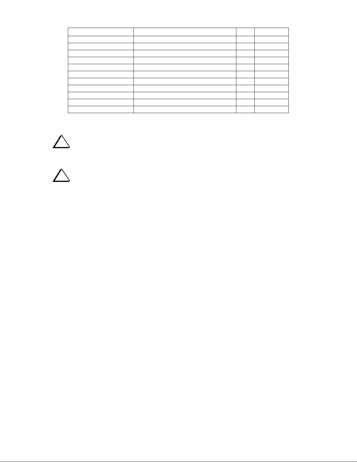
Note: A new RoHS compliant surface mount version of the PIN diodes used at D1 and D2 is supplied preinstalled on tiny printed circuit. Install the new part as follows.
5
Page 6
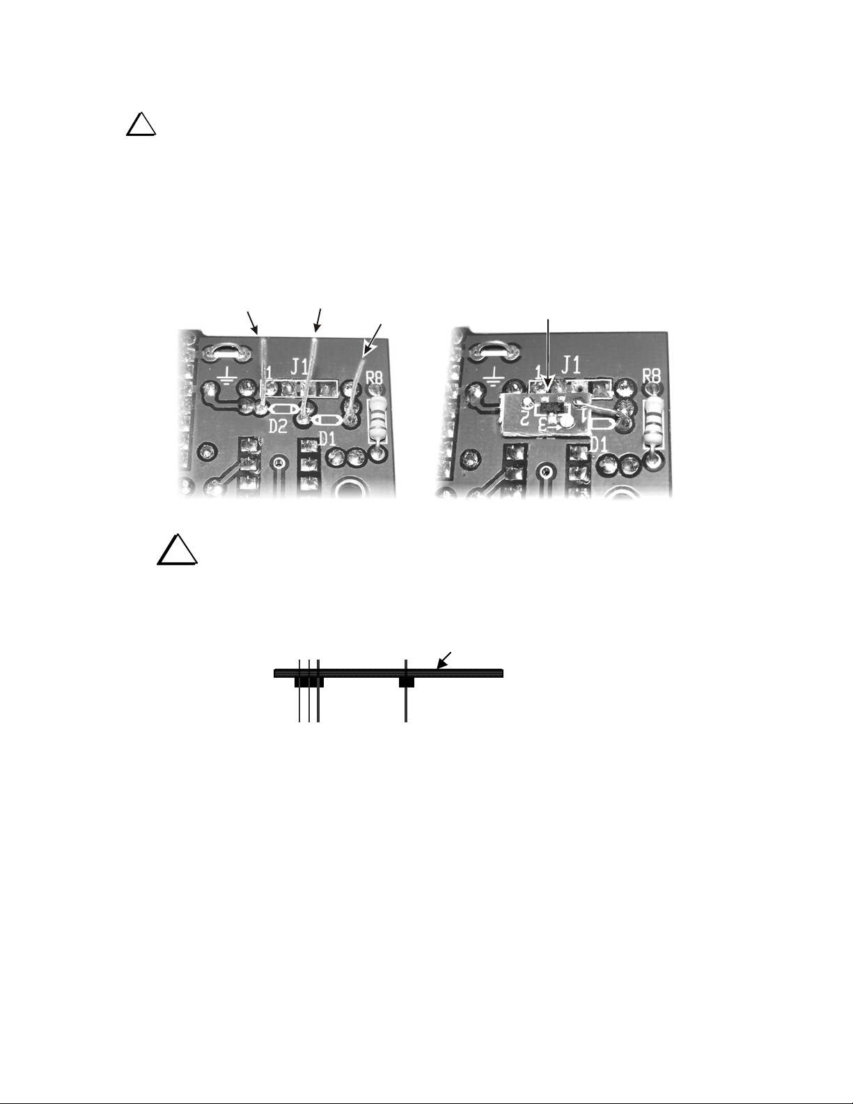
Select three of the resistor leads you saved and solder them in the pads for D1 and D2 as shown below.
e
Lead 3 goes into the solder pad for the banded end of D1. The solder pad at the banded end of D2 is not
used. Trim any excess flush on the opposite (top) side of the board .
i
ESD-Sensitive! Wear a wrist strap grounded through a 1-meghom resistor or touch an
unpainted metal ground before handling the SMT1B part in the following steps.
Thread leads 2 and 3 through the respective pads on the SMT1B board and position it close to the
K60XV board as shown. Be sure the leads go through the like-numbered solder pad s. When installed
correctly, the lettering on the SMT1B board will be upside down compared to the lettering on the K60XV
board as shown. Solder leads 2 and 3 and trim them flush.
Bend lead 1 over to pad 1 on the SMT1B board and solder. It is not necessary to insert this lead
into the pad. If you want to bend the end so it goes into the pad, be sure it is short enough that it won’t pass
completely through the SMT1B where it might short to a pad underneath.
2
3
1
SMT1B in place
i
In the following steps, do not trim the pins of P1 or P2 on the top side of the board.
Install 3-pin male connector P2 on the bottom of the PC board in the position indicated by its
component outline. Do not solder yet. The drawing below shows how P2 should appear viewed from the
front edge of the board (with the top side facing up).
Top Sid
P1P2
6
Page 7

Solder just one pin of P2 (but not the center pin, which is harder to re-heat due to the ground plane).
Verify that P2 is not tilted, and is seated completely flat. If not, re-heat the soldered pin and press down on
all of P2's pins until the connector drops into place. Once the connector is seated correctly and is not tilted,
solder the other two pins.
Install 8-pin male connector P1. (An end view of P1 is shown in the drawing above.) Solder just one
pin of P1, near the middle of the connector. Verify that P1 is now perpendicular to the PC board and is
seated completely flat. If not, re-heat the soldered pin and press down on all of P1's pins until the connector
drops into place. Once the connector is seated correctly and is not tilted, solder the remaining pins.
At this point only the locations for J1 and J2 should be empty. Use of these connectors is explained in
later steps.
Do a complete visual inspection of the PC board, on both sides, using a magnifying glass. Look for:
__ solder bridges; __ unsoldered pins; __ cold solder joints; __ backwards diodes or ICs.
This completes K60XV PCB assembly.
Installation
i
Installation of the K60XV module may require 1 to 2 hours or more to complete. Before
proceeding, you should already have installed and tested new K2 firmware if applicable (you'll need 2.04P
or later). Also, if your K2 serial number is 4087 or lower and you plan to install a replacement
heatsink/rear-panel with phono connector holes, you should have this panel available before you start.
Otherwise, you will not be able to complete the installation. (Alternatively, you can use the K2 top-cover
"XVTR IN/OUT" holes, or drill two phono connector holes in your existing heatsink panel. Both options
are covered in these instructions.)
Remove the K2's top cover or KPA100 module, unplugging all internal cables.
Remove the bottom cover panel (the panel with the tilt stand).
i
The lower rear panel/heat sink must be removed in order to install K60XV module connectors.
Follow the procedure below carefully so that none of the hardware will be lost or reinstalled incorrectly.
Remove the heat sink panel as follows: (1) remove six screws; (2) remove the hardware retaining the
antenna and key jacks; (3) if you have a 160 m module (K160RX), unplug it; (4) tilt the K2 up on its left
side, with the front panel facing forward; (5) remove the two nuts and lock washers holding the heatsink to
the PA transistors, but do not remove the PA screws; (6) push the PA screws back into the cabinet just
enough to allow removal of the heatsink panel, but do not allow the screws to fall out; (7) remove the
heatsink panel; (8) push the PA screws back down from the top side of the RF board; (9) install the two
nuts removed earlier onto the PA screws (hand tight) to hold all PA hardware in place as you complete the
remaining installation steps.
7
Page 8

K2 RF Board Preparation
Remove the nut (but not the screw or lock washer) holding driver transistor Q6 in place. Thread the
supplied 9/16" long (14 mm) nylon standoff onto the screw, from the top side of the RF board, in place of
the original nut. (The screw should be installed from the bottom.) Do not overtighten, as this might strip the
threads of the standoff.
Desolder and remove jumper W6, which is near J13 on the RF board. (J13 is close to the rear panel and
slug-tuned inductor L2.)
Locate capacitor C6 on the K2 RF board. It can be found near the striped end of the 40-meter band-
pass filter relay (K1). On revision B or later K2 RF boards, C6 is on the bottom side of the board, and the
top side is labeled "J15" at that same location, with pads for a 3-pin connector. On earlier K2 RF boards,
C6 is on the top side, and there's no "J15" label.
Remove C6, being very careful not to damage its pads or traces. Completely remove residual solder
from the holes using solder wick.
Locate the 3-pin female connector supplied with the K60XV kit, identified as RF-J15 in the parts list.
If your K2 does not have the "J15" label at the position of C6, pul l out the center pin of the 3-pin connector
using long-nose pliers. (Using just the two outer pins will have no impact on performance.)
Install the 3-pin connector on the top side of the board, at the location for C6/J15. Solder one pin first.
Once you're sure the connector is flat against the board and not tilted, solder the remaining one or two pins.
Locate the 8-pin female connector, identified as RF-J13 in the parts list. Install this connector at J13
on the RF board. Use the same technique you used in the previous step.
On the top side of the RF board in the synthesizer area, locate C71 (82 pF). C71 is near relays K13 and
K14. Desolder and remove C71.
Install a 120-pF capacitor at C71 ("121", identified in the K60XV parts list as RF-C71).
If your K2 serial number is 3000 or higher (revision B or later RF board), you'll find locations in this
area of the board for varactor diodes D19 and D20 on the top side (MV2109), and R29 should already be
installed on the bottom. Install the two varactor diodes: __ D19; __ D20. Skip the next two steps.
8
Page 9

If your K2 serial number is 2999 or lower (revision A or XC RF board), D19, D20, and R29 must be
soldered on the bottom of the board as shown in the left-hand illustration below. Solder the indicated leads
of the two varactor diodes to the pads of C71 (which is on the top side). Solder the cathode leads together,
then to one lead of R29. Solder the other lead of R29 to the indicated pad of R32 (which is on the top).
Position all three components close to the bottom of the PC board, and make sure their leads don't contact
any adjacent pads or traces. The installed height must be no more than 3/16" (5 mm).
The revision A or XC board must be modified in the area of 8-pin connector J13, on the bottom of the
board. First, cut the two traces that connect to pin 6 of J13, as indicated by the two "X" marks in the righthand illustration below (this is best done using the tip of an X-acto knife, or a very small, sharp, flat-blade
screwdriver). Next, cut a 2.5" (6.5 cm) length of green, solid-conductor hookup wire. Remove 1/8" (3 mm)
of insulation from each end. Solder this jumper to the indicated pads.
RFC10
R29
10K
D20
209
MV
209
MV
D19
RFC2
C104
R44
R4
R43
R48
C27
RFC5
9
Page 10

Turn the K2 upside down (if it isn't already), with the front panel facing forward.
Cut a 7.5" (19 cm) length of RG174 coax cable. Remove 7/8" (22 mm) of the plastic jacket at one end,
and 1/2" (13 mm) at the other. Separate the braid from the center conductor at each end using a small,
pointed tool. Then unweave the strands. Be sure to remove all broken strands, which might cause shorts.
At the long (7/8" [22 mm]) end, cut away about half the strands, then twist together and tin those that
remain. Trim the prepared length of braid back to about 3/8" (9 mm) long.
At the short end, cut off all the strands. Cover the exposed braid with 1/2" (13 mm) of heat-shrink
tubing. Shrink the tubing using a high-temperature heat gun or a match (keep flame 1" away from tubing).
Strip off 1/8" (3 mm) of insulation from the center conductor at each end. Twist and tin the strands.
Place the coax cable as shown in the drawing below. The end with the longer center conductor will
terminate near 8-pin connector J13, which was installed earlier on the top side of the board.
At the J13 end, solder the braid to the indicated pad of L4 (ground).
Solder the center conductor into the hole just left of J13 pin 6 (labeled "X" on the board), or, if your
K2 s/n is 2999 or lower, to pin 6 of J13 itself. Count the pins of J13 carefully. The round pad is pin 1.
At the other end, solder the center conductor to the "RF" pad on the board, or, for K2 s/n 2999 and
lower, to the pad of R66 that's closest to the front panel. (Remove the KNB2 module to locate R66.)
To keep the coax cable in place, use a short length of the green-insul ated, solid conductor hookup wire
as a retainer. Solder the wire in the position shown, using only the two indicated pads. These two pads are
already connected together on the top side of the RF board. Do not use any othe r pa ds.
C104
Ground to
L4 here
C
C216
C207
C204
C224
C208
80m
C195
RFC6
R50
R47
R65
RFC2
G
R48
8T
E
R43
RFC5
B
R34
1
Q7
RFC8
RFC9
Q8
R63
RFC4
C119
Jumper
G
RF
Clip braid
C161
R
I
R75
E
C
B
10
Page 11

Heatsink/Lower Rear Panel Preparation
If you wish to modify your existing heatsink panel for use with phono connectors, do so now, using the
drilling template below. Position the holes exactly as shown to ensure that the connectors do not
interfere with the K60XV module or parts on the RF board. Use a small pilot bit before drilling the
final holes. You'll may need to move the K2's serial number label to the right. If it becomes damaged when
you remove it, you can obtain a replacement from Elecraft.
XVTR
(1.40 cm)
KEY
RX
ANT
IN OUT
0.28
dia
0.55
(7.1 mm)
0.52
(1.32 cm)
3.02
(7.67 cm)
If you plan to substitute a new heat sink, move the 160-m module and RX ANT jack (if applicable),
two rubber feet, and serial number label from the old panel to the new one. If the serial number label
becomes damaged when you remove it, you can obtain a replacement from Elecraft.
Replacement thermal pads are supplied for the PA transistors (Q7 and Q8). Use these replacements if
the original pads appear to be damaged in any way. (See Figure 6-32 in the K2 Owner's manual.)
Turn the K2 up on its left side, with the front panel facing forward.
Re-install the heatsink panel as follows, also referring to Figures 6-33 and 6-34 of the K2 Owner's
manual if necessary: (1) carefully remove the two nuts holding the PA transistor hardware together (don't
let the hardware fall out); (2) push the PA screws back into the cabinet (from the bottom side) just enough
to allow installation of the heatsink; (3) install the heatsink (fig. 6-33); (4) install the two nuts and lock
washers that retain the PA transistors (do not overtighten); (5) install six screws, starting with the two
between the PA transistors (fig. 6-34); (6) install the hardware retaining the antenna and key jacks; (7) if
you have a K160RX module, plug it into J14 on the K2 RF board. The K2 can now be returned to a
horizontal orientation.
Using an ohmmeter on its lowest scale, measure the resistance to ground from the collectors of Q7 and
Q8. If there's a short (< 10 ohms), remove the heat sink and investigate the cause. The most likely reason
for a short is mis-alignment of a shoulder washer or thermal pad.
11
Page 12

Transverter Connector Installation
You can use either the original top cover XVTR IN/OUT holes (not applicable if you have a KPA100
installed), or phono jacks on the lower rear panel/heatsink. Both installations are covered below.
1.
If you'll be using the original XVTR IN/OUT connectors on the top cover (BNC):
Remove any masking tape from the BNC holes in the top cover. If the inside surface is painted,
scrape or sand away sufficient paint for the connectors to make good contact.
Install BNC connectors in the XVTR IN and OUT holes, including the supplied solder lugs.
Cut two 4" (10 cm) lengths of RG174 coax cable.
At each end of the coax cables, remove 1/2" (13 mm) of the plastic jacket. Separate the braid from
the center conductor using a small, pointed tool. Cut away about half the strands, then twist together
and tin the remaining strands. Also twist and tin the strands of the center conductor.
Solder one end of a coax cable to the OUT jack (center conductor to the center pin, and shield to
the solder lug). Solder one end of the other coax cable to the IN jack.
Solder the free ends of the two coax cables to the pads of J1 on the top side of the K60XV board:
__ OUT center pin to J1 pin 1, shield to J1 pin 2 __ IN center pin to J1 pin 4, shield to J1 pin 3
Make sure that the coax cable shield wires are not touching any component leads.
2.
If you'll be using phono jacks on the lower rear panel/heatsink:
Remove any masking tape from the phono jack holes in the heatsink. If the inside surface is
painted, scrape or sand away sufficient paint for the connectors to make good contact.
Install phono jacks in the XVTR holes in the heatsink, using 1/4" lock washers inside and outside.
(see drawing below). Use a solder lug on the left connector only, folding the lug away from the panel.
Note: These jacks can be tightened from the rear of the panel due to their hex-shaped flanges.
Prepare three 1" (25 mm) jumpers using #24 stranded hookup wire (black insulation). Strip 1/8"
(3 mm) of insulation from each end. Twist the strands together, then tin them very lightly.
Solder one wire to each phono jack as shown. Solder the third wire to the lug.
To see the location of the K60XV module relative to the two jacks, plug it in temporarily (P2 to
J15 on the RF board, P1 to J13). Unplug it and tilt its front edge upward to gain access to the pads of
J1. Insert the free ends of the three wires into the K60XV PC board at J1 pins 1, 2, and 4 as shown,
from the bottom side. Then fold the K60XV downward to gain access to the top side, and solder.
OUT
P2
(P2 and P1 are on
bottom of PC board)
12
P1
1
2
2
IN
K60XV
PC Board
4
Wires routed to J1
from underneath
Page 13

K60XV Module Installation
If a K160RX option (160 m and Receive Antenna) is installed, you may need to adjust the position of
the RX ANT ground lug to prevent interference with the K60XV board in the next step. This ground lug
should not be rotated to face upward, as it may contact one of the top-cover option modules (KAT2 or
KPA100). The lug should instead be rotated so that it is either below the RX ANT jack or so it fits into the
cutout on the K160RX module.
Plug in the K60XV module. Make sure the 3- and 8-pin connectors, P2 and P1, are properly mated
with J15 and J13 on the RF board. There will be some length of pin exposed on each connector, so that the
K60XV PC board height matches the height of the nylon standoff. Three slug-tuned inductors on the K2
RF board should appear approximately centered in the associated holes on the K60XV board.
i
The three slug-tuned inductor holes are provided so you can access all of the K2's band-pass filter
alignment points without removing the K60XV. However, it should normally not be necessary to adjust
these inductors during K60XV alignment.
Secure the K60XV module to the nylon standoff using a 4-40 x 1/4" (6 mm) screw and one #4 split
lock washer. Do not overtighten the screw, which could strip the threads in the standoff.
Re-install the bottom cover.
Verify that your K2 firmware is at revision 2.04P or later (by holding any key during power-on). If not,
you must upgrade it before you can complete K60XV alignment and test. Refer to the instructions supplied
with the firmware.
If you have a KAT2 internal ATU and its firmware has not already been upgraded to 1.07 or later, you
may want to upgrade it now. The KAT2 may be usable on 60 meters with an older revision of firmware,
but it will not cover a very wide impedance range.
If you have a KPA100 100-watt stage and you plan to use it on 60 meters, it must be upgraded as noted
on page 2 of this manual. If you choose not to upgrade it at this time, be sure not to attempt to transmit in
high-power mode on 60 meters.
This completes K60XV installation.
Note: Do not install the top cover or the KPA100 module at this time.
13
Page 14

Alignment and Test
Initial Test
Turn on the K2. If you see INFO 080 or the receiver is muted, refer to Troubleshooting.
Enter the K2 menu by tapping MENU. Tap DISPLAY to switch to the secondary menu (you'll see
SEC on the display). Then locate the D19 menu e nt ry usi ng BAND+ / BAND- or the VFO knob.
Edit the D19 menu entry by holding EDIT. Use BAND+ or BAND- to set D19 to Y (meaning
yes, D19 and D20 are installed). Exit the menu by tapping MENU twice.
Use BAND+ and B AND- to switch to the 60-meter band, which should appear between 80 and 40
meters. (If a band does not appear between 80 and 40 meters, see Troubleshooting.)
Due to recent firmware changes, the frequency of this band may initially be set to something other than
the 5 MHz range. If so, use direct frequency entry to enter a frequency of 5000 kHz for VFO A. To do
direct frequency entry, hold
5 0 0 0 using the numeric keys on the right side of the front panel. Then copy VFO A to VFO B by
tapping A=B .
BAND+ and BAND- together until you see "----" on the LCD, then enter
You should now be able to tune the 60-meter band using the VFO knob. If not, see Troubleshooting.
40 / 60 Meter Alignment
Connect the (+) lead of a DMM (digital multimeter) to the lead of R30 nearest the case side panel (R30
is in the synthesizer area of the K2 RF board). Use a small alligator clip to ensure a good connection.
Connect the (-) lead to one of the ground jumpers on the RF board. Set the DMM for to measure DC volts,
10 V or higher full-scale.
Switch to 40 meters. Set the VFO first to 7000, then 7300 kHz, noting the DMM's voltage readings at
each frequency. Switch to 60 meters and perform the same test at 5300 and 5450 kHz.
If any of the above readings are below 1.0 V or above 7.5 V, you'll need to re-adjust the VCO inductor,
L30, as explained under VCO Alignment in the Alignment and Test, Part II section of the K2 Owner's
Manual. Note: Add 60 m (and 160 m, if applicable) to the list of bands shown in Table 6-1, and use 1.0 V
as the minimum, not 1.5 V. If you're unable to find an acceptable setting for L30, see Troubleshooting.
Connect an antenna to the K2. While listening to and noise or a weak signal, use a small flat-blade
screwdriver to peak the two trimmer capacitors on the K60XV module (C1 and C2). The screwdriver used
can have a metal handle since the rotors of the trimmers are grounded.
Connect a dummy load to the K2. Set the POWER control about 2 watts.
Enter TUNE mode, then adjust the two trimmers for maximum transmit output. Cancel TUNE.
Set POWER to 10 watts. Verify that you can reach this level in TUNE mode on both 40 and 60 m.
Re-install the top cover or KPA100 module, re-connecting all of the internal connectors. Secure it with
six screws. If you're re-installing a KPA100, be careful not to overtighten the side-panel screws.
14
Page 15

i
page 2, you must not use it on 60 meters. The signal will not meet K2 spurious emission specifications,
and you could damage the final amplifier transistors.
If you have a KPA100 100-watt stage installed that has not yet been upgraded as explained on
If you have a KPA100 installed that includes recent upgrades as explained on page 2, set power to
about 50 watts. Otherwise skip the next two steps.
Connect an appropriate dummy load and power supply for high-power operation.
Using TUNE mode, verify proper power output on 60 meters.
Read the 60-meter operating instructions starting on the next page before transmitting on this band.
Low-Level Transverter I/O Test
Tap MENU. Tap DISPLAY to switch to the secondary menu (SEC). Locate the TRN1 menu entry
using BAND+ / BAND- or the VFO knob. Hold EDIT to edit the parameter, and set it to ON.
Tapping DISPLAY scrolls through the various transverter setup fields. Tap DISPLAY and set RF
to 50 MHz. Then set IF to 28 MHz, OFS to 0.00, and ADR to TRN1.
Tap DISPLAY once more to get to the OUT (power output) field. As you rotate the VFO knob
you'll find that this field has two consecutive ranges: L0.01 - L1.27 and H0.1 - H12.7. The L
settings select the low-power I.F. output (XVTR jacks) and set the maximum power level in milliwatts. The
H settings select the normal high-power path and set the maximum power level in watts. For now, set
OUT to L1.00 (1.0 milliwatts, low-power output enabled). Then tap MENU twice to exit the menu.
Change bands to the first band above 10 meters, TRN1, which you assigned to 6 meters (50 MHz).
The display may be incorrect initially due to recent firmware changes. If so, you'll need to use direct
frequency entry one time to correct the display. To do direct frequency entry, hold
together until you see "----" on the LCD, then enter 5 0 0 0 0 using the numeric keys.
BAND+ and BAND-
Copy VFO A to VFO B by tapping A=B .
If you have a signal generator capable of operation in the 28 MHz band, set it to a low level (-80 to
-100 dBm) and connect it to the XVTR IN jack. If you only have a higher-power signal source, couple it
loosely to the XVTR IN jack using a length of wire, or use an attenuator.
The K2 frequency display is now set up such that a 28000.00 kHz signal at the XVTR IN jack should
be properly tuned in at
50000.00 MHz indicated. Verify this using your signal generator.
Connect a 50-ohm dummy load (or a resistor as close as possible to 50 ohms) to the XVTR OUT jack.
Switch to CW mode. Set the POWER control for approximately 1.0 milliwatts. P1.00 LP will be
displayed, where
LP is a reminder that you're using low-power transverter I/O on the present band.
Enter TUNE mode. The bargraph should be at full scale (indicating 1.0 mW) and the LCD should also
indicate a power output of approximately 1 milliwatt. (If not, see Troubleshooting.) Cancel TUNE.
15
Page 16

Using the K60XV
Note: If you remove the K60XV, you'll need to reconnect the RF path on the K2 RF board in two places:
(1) insert a 4.7-pF capacitor into pins 1 and 3 of J15; (2) in sert a jumper between pins 3 and 5 of J13. Leave
all RF board components you installed in place, and leave the
and low-power transverter I/O will no longer be available, but the K2 should otherwise function normally.
60 Meter Operation
Before proceeding, you should become familiar with the 60-meter regulations in your country or
region. Detailed information is available for the following entities (check our web site for others):
D19 menu entry set to Y. The 60-m band
U.S.: http://www.arrl.org/FandES/field/regulations/faq-60.html
United Kingdom: http://www.rsgb-hfc.org.uk/operating%20procedures.htm
Enabling 60 meters: To use the K60XV on 60 meters,
D19 must be set to Y, and the associated
hardware changes must be in place (C71 = 120 pF; R29, D19, and D20 installed).
U.S. 60-meter frequencies: The 60-meter U.S. amateur allocation provides five fixed-frequency, USB-
only channels with a width of 2.8 kHz. The FCC specifies t he frequencies as having channel centers of
5332, 5348, 5368, 5373, and 5405 kHz. Since the only allowed operating mode is USB, this corresponds to
ham transceiver VFO frequencies of 5330.5, 5346.5, 5366.5, 5371.5, and 5403.5 kHz. The K2 can be set up
to channel-hop among these frequencies as explained on the next page. Note: 5403.5 kHz is available in
both the U.S. and U.K. 5371.5 kHz is used by the HF Pack group (http://groups.yahoo.com/group/hfpack/)
U.S. power limit: The maximum power output on 60 meters is the amount that, with a given antenna,
would be equivalent to 50 W into a dipole. The ARRL and other sources provide additional guidelines.
ATU Use on 60 Meters (KAT2, KAT100): If your regulations allow brief CW transmission on 60 meters,
you'll be able to use our KAT2 or KAT100 ATUs on thi s b a nd (y ou'll need KAT2 firmware revision 1.07,
or KAT100 revision 1.05). Both tuners will match nearly any antenna on this band, can function with as
little as 0.5 watts, and save their matching parameters in nonvolatile memory for instant recall on band
change. Since 60 meters is a relatively narrow band, you will in most cases only need to tune a given
antenna up once, near the middle of your allocation.
Resonant antennas, and getting by without an ATU: CW operation is not permitted on 60 meters in the
U.S. This presents a problem for automatic antenna tuners, which require either a carrier or a sustained
voice signal, such as a whistle, in order to do antenna matching. (In SSB mode, a whistle is essentially a
1
carrier
.) To get around this, you could put up a resonant antenna, or use a manual tuner in conjunction with
an antenna analyzer. If an ATU will still be left in-line, you can either set it for bypass mode, or pre-tune it
into a dummy load on 60 meters.
.
1
The KAT2 and KAT100 use the carrier method, which is faster and more reliable than whistling.
Whistling may also be frowned upon by some users of the band.
16
Page 17

Using the KPA100 on 60 meters: The KPA100 can only be used on 60 meters if it includes recent
modifications (see page 2). Otherwise, it could be damaged. Note: Normally, the 40/30 meter low-pass
filter on the KPA100 is used on 60 meters. This filter rolls off aggressively above 10.15 MHz. Combined
with the KPA100's excellent PA balance, this results in adequate 2
nd
-harmonic rejection when the K2/100
is operated from 5300-5500 kHz. However, a future application note will explain how to modify the
KPA100's 80-meter low-pass filter to work on 80 and 60 meters. This would provide much better rolloff if
needed. The
D19 menu entry can be used to select which KPA100 low-pass filter to use. When editing the
D19 parameter, tap DISPLAY to select PA60= 80 or PA60= 40 (default). Leave D19 set for
PA60= 40, even when using KPA100 kit revision C. (See Important Operating Notes on pg 19.)
Channel Hopping and Scanning (Applies to HF and Transverter Bands)
Channel hopping, if enabled, allows you to use the VFO knob to quickly hop among just those frequency
memories which fall into the present ham band. You can turn this mode on or off on a per-band basis
(default is off). Channel scanning—among these same memories—can also be enabled on a per-band
basis. It will work in either the original K2 scan mode (receiver muted) or in "live scan" mode, where the
receiver is not muted, and scanning doesn't stop until you touch any switch. To use these features:
1. RCL memory # 9 to see if it is set up for 5000 kHz (one of the original defaults). If it is, and you plan
to use channel scanning on 60 meters, you should store a different frequency in this memory (on a
different band). Otherwise you may hear WWV at 5 MHz during 60-meter channel scanning.
2. Set up and STORE two or more frequency memories within the target band (using VFO A). Frequent
users of 60 meters in the U.S. should set up memories 1 through 5 as USB, on the allocated channels
(5330.5, 5346.5, 5366.5, 5371.5, and 5403.5 kHz). Note: 10 frequency memories are available in the
K2, so using five of them on 60 meters will leave just five for other purposes. You can use fewer than
five on 60 meters if desired.
3.
Choose one of the stored memories as an "initializer" to be used when starting channel scan on this
band, and RCL it. (For 60-meter users, this would typically be memory # 1.)
4. Edit the RATES secondary menu parameter. Tap DISPLAY to select CH SC (channel scan
enabled) or CH SC-TN (channel scanning and manual channel tuning enabled). Note: The nor
(normal) setting of this parameter disables both.
5. Exit the menu, then STORE this memory (using the one you recalled in the previous step). If manual
channel tuning is enabled, you can now use the VFO to hop among memories assigned to this band.
6. To start channel scanning on the desired band, hold RCL , then hold the numbered key corresponding
to the "initializer" memory you saved earlier, e.g. 1 . Holding the numbered key for about 1/2 second
will show
ON
7. You may wish to program PF1 or PF2 as a scan resume function, using the PF1 or PF2 menu
entry. This will allow you to quickly re-start scan from where it left off. As with the RCL method, you
can hold PF1 or PF2 for about 1/2 second to start normal scanning, or hold for an additional 2
seconds to start live scanning (AF ON).
SCAN on the LCD. If you continue to hold the key for another 2 seconds, you'll see AF
, initiating "live" (unmuted) scan.
Using RIT and XIT with channel hopping: If you have channel hopping enabled, and you need to finetune your operating frequency, simply turn on both RIT and XIT at the same time. The RIT/XIT offset
potentiometer will then function as a limited-range VFO control, moving RX and TX frequencies equally.
17
Page 18

Transverter Operation
Basic transverter use: The K2 acts as a high-performance I.F. transceiver for nearly any type of
transverter, and is especially flexible with the K60XV installed. The K2's
to specify the RF band to be displayed, your choice of five I.F. bands, and per-band settings for frequency
correction, transverter selection, and power output level. If you have never used transverters with the K2
before, you should familiarize yourself with the transverter band setup information in the K2 Owner's
Manual (in the Secondary Menu Functions section) . If you're using Elecraft XV-series transverters, please
also review their manuals for instructions regarding K2-related connections and configuration. (Some
information in this manual may supercede that in the XV-series manual.)
Transverter bands and frequencies: You can define up to 6 transverter band displays. Once enabled, they
will appear above 10 meters in the band rotation. To set them up, use the
entries. (
menu entry has a number of fields, accessed by tapping DISPLAY . The RF field can be set from
TRN4-TRN6 use the same three entries, but are accessed by tapping ANT1/ 2 .) Each TRNx
0 through 999. For bands over 999 MHz, enter only the low-order MHz digits (e.g., for 1296 MHz, use
296). The IF field can be set to 7, 10, 14 , 21, or 28 MHz. The OFS field can be used to specify an
oscillator/multiplier chain correction of up to +/- 9.99 kHz. (See below for details on other fields.)
TRNx menu entries allow you
TRN1-TRN3 secondary menu
Transverter selection and control: Using the
specify which specific Elecraft XV-series transverter should be enabled when you switch to each
transverter band display. This is especially useful with the XV144, which is often used as an I.F. for
multiple microwave bands. XV series transverters include an address selection switch that must be set up to
match the value in the
the binary value of the ADR field on three pins of J2 for use with transverters from other manufacturers.
These signals must be externally bypassed and buffered if they are to be used for transverter control. Note:
The Elecraft KRC2 universal band decoder also decodes the
drive outputs for use with transverters or other gear.
Transverter keying: Elecraft XV-series transverters are keyed via the 8R line, available via the AUX I/O
connector on either the KIO2 or KPA100 module. Third-party transverters can be keyed via an external
hardware interface derived from the 8R line. An alternative, if relay drive requirements are low, is to use
the K60XV's built-in transverter keying device (a 2N7000 MOSFET). The keying signal is available on J2.
Using low-power and high-power transverter I/O: The
range: L0.01-L1.27 (milliwatts) and H0.1-H12.7 (watts). In both cases these are upper limits, and
the POWER knob can be used to go down from there. Low-power (0.01-1.27 mW) settings require the
K60XV option. (The low-power detector works best if you avoid POWER settings under 0.10 mW.) The
low-power TUNE display shows, for example, P1.00 LP, where 1.00 is the power in mW and LP
indicates that the low-power output on the K60XV is selected (high-power path disabled). Full-scale on the
bargraph is 1.0 mW in
used, along with an upper limit from 0.1 to 12.7 watts.
100's of MHz digit: If you select 10 Hz VFO steps on a transverter band whose RF parameter is set for 100
MHz or higher, the 10-Hz digit is only shown for 1 second, then the display shifts to the right. This allows
the hundreds of MHz digit to always be displayed.
ADR field. (Refer to the XV series manual for details.) The K60XV also outputs
LP mode. The H settings specify that the K2's normal high-power path should be
ADR (address) field of the TRNx menu entries, you can
ADR value, and provides numerous relay
TRNx menu entries' OUT parameter has a dual
18
Page 19

Important Operating Notes
1. Using the KPA100 on 60 meters: Recent KPA100 kit modifications (revision C) allow high-power
operation on 60 meters. However, these changes do not include a revised 80-meter low-pass filter. For 60
meters, you’ll still use the KPA100’s 30/40-meter low-pass filter. For this reason, you must leave the K2’s
D19 menu parameter set for PA60=40 (see K60XV manual).
2. Using TUNE mode with the K60XV and an ATU: If the ATU is in either of its autotune modes
(
AUTO or ALT), and you’re on a transverter band configured for LP mode (Low Power, 0 dBm), holding
TUNE drops power to 0.2 milliwatts maximum. You can override this behavior by holding DISPLAY
along with TUNE, or by selecting any ATU mode other than AUTO or ALT in the menu.
3. KAT2 modification for use with K60XV LP mode: In some cases the LM358 op-amp on the KAT2
can load down the K60XV's low-power RF detector (at the emitter of Q2), preventing the K60XV from
developing a full 0 dBm (1 milliwatt) signal at the transverter OUT jack. To correct this, change R6 on the
KAT2 from 47 ohms to 470 ohms. This resistor is supplied with the K60XV kit. R6 is on the bottom of the
KAT2 control board, and can be changed wi tho ut removing the KAT2 module.
19
Page 20

Troubleshooting
i
If your specify problem is not covered below, re-check component values, diode and IC
orientation, and look for soldering problems (bridges, leads not sold ered, cold solder joints).
If the S-meter shows full scale and the receiver is always muted: The coax cable on the bottom of the
board may be connected to some pin other than pin 6 on J13.
If the 60 meter band is not available between 80 and 40 meters, or if you see
LCD: You may have the K60XV module plugged in incorrectly at J13 (8-pin connector). If not, you could
have a problem with the microcontroller on the K60XV (U1). Unplug the K60XV module and examine U1
closely for bent pins or pins not inserted into the socket. Make sure U1 is not plugged in backwards, and
that you have the correct values of R1 and C12 installed. Also examine Z1 for possible heat damage.
If signals on 40 and 60 meters can be heard, but are distorted or can't be tuned in using the VFO:
Verify that C71 on the RF board has been replaced with a 120 pF capacitor. Also check for correct values
and proper installation of R29, D19, and D20 (on the bottom of the board if your K2 s/n is 2999 or lower).
If L30 on the K2 RF board cannot be adjusted so that the VCO voltage is in the 1.5-7.5 VDC range
on all HF bands: Use the troubleshooting information given in the previous item (C71, D19, D20, etc.).
If you can hear signals on all bands except 40 and 60 meters: You may have the K60XV module
plugged in incorrectly at J15 (3-pin connector). Also look for shorts around P2 or K1 on the K60XV.
If the K60XV cannot reach 10 watts on 40 or 60 meters (KPA100 bypassed or not installed): The 40-
m band-pass filter inductors or 60-meter trim caps may not be aligned correctly, or you could have an
incorrect value capacitor at C2-C6 on the K60XV boar d.
If the KPA100 draws excessive current when used on 60 meters: Make sure you have not accidentally
selected the KPA100's unmodified 80-meter low-pass filter for use on 60 meters (see the
discussion at the end of the paragraph, Using the KPA100 on 60 meters). Also, verify that your KPA100
includes recent changes required for operation on this band as described on page 2.
If the low-level XVTR OUT signal is too low in amplitude (< 1 milliwatt into 50 ohms): Re-peak the
band-pass filter for the I.F. band in use. Also check D1 and D2 on the K60XV board, as well as other
components in the low-power path, for correct value and proper orientation.
INFO 080 on the
D19 menu
If the bargraph or LCD power display do not read properly during low-power transverter use:
Check the installation of the coax cable on the bottom of the RF board, as well as D1, D2, and all
transverter ALC detector components on the K60XV PCB. Avoid using POWER settings under 0.1 mW.
If the K60XV module has been removed
all bands: Having removed the K60XV, you must reconnect the RF path on the K2 RF board: (1) insert a
4.7-pF capacitor into pins 1 and 3 of J15; (2) insert a jumper between pins 3 and 5 of J13. Leave D19, D20,
and the other added components in place, and leave the
low-power transverter I/O will no longer be available, but the K2 should otherwise function normally.
If SSB power control malfunctions with transverters: KSB2 revision 1.07 or later firmware is required.
20
, and the K2 does not receive or transmit on 40 meters or on
D19 menu entry set to Y. The 60-meter band and
Page 21

Circuit Details
(Refer to the schematic on the next page.)
The K60XV has two distinct functions: 60 meter band-pass filtering, and low-level transverter interface.
Both are under control of microcontroller U1, which receives configuration commands from the K2 via the
AuxBus. U1 drives latching relays K1 and K2; provides transverter control outputs (keying, address
selection) that can be used with non-Elecraft transverters; and enables the transverter low-level I/O path
when it's selected by setting /LP to 0V and 6LP to 6 volts (see discussion below).
Relay K1 and associated components re-resonate the 40 m BPF on 60 meters. P2 provides the interface to
the 40-meter filter on the RF board.
The XVTR ALC circuitry acts as a compensated linear power detector. It converts a 0 dBm (1 mW)
transverter output level to about 3.6 VDC. This means the bargraph will be full-scale at 1.0 mW, with 0.1mW increments. Rev 2.04 K2 firmware also properly displays power in the LP case, from 0.01 to 1.27 mW
(e.g.:
P1.20 LP).
When 6LP is low (i.e. when the low-level split-path interface is not in use), buffer Q2 (2N2222) looks like
a high impedance to VRFDET. But when the LP interface is in use, 6LP is high, powering U2, and Q2 acts
as a buffer for U2's output, allowing it to easily override the combined impedance of the K2's standard
power metering circuit and a KAT2 or other ATU if present. When the split path is in use, K2 firmware
turns off the VRFDET signal buffers on the KAT100 and/or KPA100 if present.
The circuit at upper right provides XVTR T/R control and signal routing. Normally relay K2 is reset,
looping the BPF signal back to TX IN (the input to the K2's 10W transmit strip) and AC-shunting the
transverter RF path to ground. If the operator switches to a transverter band configured for low-level I/O,
K2 is set. This AC-grounds the input to the 10W PA strip (K2A) and routes the BPF output signal to the
XVTR TX and RX PIN diodes, D2 and D1 respectively. At the same time, the MCU (U1) grounds the /LP
signal (U1-3 is an open-drain output), allowing D1 or D2 to be forward biased.
In RX mode, 8R is high, forward biasing D1; in this case switch Q1 (2N3906) is open, and D2's anode is
held at 0 V by R10 (near the bottom of the sheet). In TX mode, 8R is near 0 V, turning on Q1 and placing
6V on the 6T line. This turns on D2, while D1 is now reverse biased. Also in TX mode, Q3 (2N7000) turns
on. The drain of Q3 is routed to pin 2 of J2.
The low-going TX signal at pin 2 of J2 could be used with non-Elecraft transverters to do transmit keying.
Elecraft XV Series transverters have a connection to the 8R line for keying purposes. The logic-level
outputs on J2 represent the binary value of the ADR parameter in the TRNx menu entries. These signals
could, with proper buffering and RF bypassing, be used to turn transverters on or off. XV Series
transverters obtain their physical address via the AuxBus, so these connections are not needed.
Elecraft • www.elecraft.com • 831-662-8345
Page 22

K60XV Schematic
22
 Loading...