

Page 1

Asse m b ly a nd O pe ra tio ns Ma nua l
Z10000 Bro a db a nd Buffe r Am p lifie r
®
Ele c ra ft
K2 Ve rsio n & Unive rsa l Ve rsio n
Version 3.2.1 / 05 January 2009
7236 Clifton Road
Clifton Virginia 20124
Telephone: (703) 830-0368
Fax: (703) 830-0711
http://www.cliftonlaboratories.com
Page 2

Asse m b ly a nd O p e ra tio ns Ma nua l
Z10000 Bro a db a nd Buffe r A m plifie r
Elec ra ft® K2 Ve rsio n & Unive rsa l Ve rsio n
Version 3.2.1 January 2009
(c) 2006, 2008, 2009 Jack R. Smith d/b/a/ Clifton Laboratories.
Last Revised 05 January 2009
Page 3

1.0 Intro d uc tio n a nd Sp e c ific a tions
1.0 Intro d uc tion
Clifton Laboratories’ Z10000 IF sampler buffer amplifier is available in two versions:
• Z10000-K2 model—A version optimized to be used with an Elecraft K2 transceiver,
with bandpass response shaping for a 4915 KHz IF;
• Z10000-U or “Universal” model—The same PCB as the Z10000-K2, but without the
frequency-dependent parts. The Z10000-U is broadband.
The Z10000 is intended to provide a high impedance interface to Clifton Laboratories’
Z90 and Z91 SpectraScan Panadapter, but may also be used as a general purpose buffer
amplifier.
1.2 Spe cific a tio ns
The Z10000-K2 and –U models share many specifications:
Pa ra m e te r C o m m o n to Z1000 0 - K2 a nd Z10 000- U
Physic a l size Approx 1.4” (35 mm) x 1.25” (32 mm). Height
approx 0.2” (5 mm) plus clearance for wiring.
Mounting hole: clearance for 4-40 machine
screw.
Po we r Re q uire m e nts +12V at approx 20 mA. On board regulator
permits operation with 30V maximum supply
voltage.
C o nne c tors None. Direct wire (coaxial cable) connection
via solder pads. User may install headers (0.1”)
spacing if so desired.
G a in User settable via programming resistor.
Different maximum and minimum for –K2 and
–U models.
O utput Im p e da nc e 50 ohms; short circuit protected.
Ac tive De vic e s 78L09 voltage regulator
AD8007 amplifier
Re ve rse Isola tio n Typically 80 dB at 4.915 MHz; depends on
cable routing as stray coupling becomes
important at this level of isolation. Less
isolation at higher frequencies. See Section
1.3.3.
Ha rm o nic Disto rtio n
nd
a nd 3rd
(2
ha rm o nic)
Typically 80 dB below carrier; depends on
gain setting and input level
3rd o rd e r
intermo d ula tio n
distortion
Typically -70 dB below output for signal levels
found in receiver input stages. IP3 depends
on gain setting and frequency, typically +30
dBm.
Clifton Laboratories – Buffer Amplifier Assembly and Operation Page 1
Page 4

Input Sig na l Le ve l DC not to exceed 25 volts; AC input level
depends on gain setting; typically used with a
less than 100 mV PP input.
Pa ra m e te r Z1000 0 - K2 Z1000 0 - U
Ba nd wid th Flat within ±1 dB over
200 KHz range
centered on 4915
KHz. Rolled off above
6 MHz and below 4
MHz.
Input Im pe d a nc e Depends on bias
isolation resistor
setting; used to
provide extra roll off
and loss;
recommended
values range from 1 K
to 4.7K ohm
G a in Depends on R905 &
R907 values. Typical
maximum gain at
4915 KHz is +9 dB,
typical minimum gain
is -18 dB
1.3 Typ ic a l Pe rform a nc e Me asure me nts
Depends on gain. If
set for +6 dB net gain,
usable bandwidth >
100 MHz. (See typical
performance plot)
Low frequency
response extends to
1
below 50 KHz.
Depends on
frequency and
attachment
technique. Greater
than 1.5 K ohm to 10
MHz, (See typical
performance plot)
Depends on R907
value. Typical
maximum gain at 5
MHz is +14 dB, typical
minimum gain is -4 dB
The data presented was taken with several Z10000 amplifiers.
• Unit 1
—A production model Z10000-U buffer amplifier equipped with connectors
for easier testing, set for net 10 dB gain (nominal2). R905 = 4.7K and R907 = 95.3
ohms. A 49.9 ohm surface mount resistor was installed across the test amplifier’s
input to provide for 50 ohm nominal input impedance.
• Unit 2—A production model Z10000-K2 buffer amplifier, set for a nominal loss of 9.5
dB. (The K2 has significant gain ahead of the recommended Z10000 connection
point; hence to provide net 0 dB from K2 antenna port to Z10000 output requires
the buffer amplifier to operate with signifcant negative gain (loss).
• Unit 3—A prototype Z10000-U ampllifier, set for 6.7 dB nominal net gain.
1.3.1 Fre que nc y Re sp o nse a nd G a in
1
It is possible to extend the Z10000’s low frequency response to 3 KHz by replacing all 0.22µF
capacitors with 1.0µF. The Z10000-U used in the test data presented has this modification.
2
The theoretical gain for the tested configuration is 9.9 dB, representing 15.9 dB amplifier
gain, followed by 6 dB loss resulting from the series 49.9 ohm output series resistance.
Clifton Laboratories – Buffer Amplifier Assembly and Operation Page 2
Page 5

The data presented in this manual was taken with two vector network analyzers; a
Hewlett Packard model 8752B and an HP model 87510A. Both VNAs assume the device
under test is terminated with the network analyzer’s impedance, 50 ohms (The 8752B is a
75 ohm test set and is used with minimum loss 75:50 ohm matching pads for all
measurements presented.) Since the buffer amplifier’s impedance significantly exceeds
50 ohms, a
nearly doubling (+6 dB gain) into a high impedance load. To prevent this effect from
distorting the gain results, all amplifiers under test have their input is terminated with a
49.9 ohm shunt resistor.
At 5 MHz, Unit 1’s measured gain is 9.78 dB, only 0.12 dB less than theoretically predicted.
The 3 dB bandwidth extends from 3 KHz to 174 MHz.
false gain will be observed due to the network analyzer’s output voltage
Unit 2, presented below, shows the effect of the K2-specific frequency shaping
components. Both above and below the K2 IF frequency (4.9 MHz), the Z10000-K2’s gain
rolls off. At the desired 4.9 MHz, the net gain is -9.6 dB, necessary to offset the K2’s post-
mixer ampllifier gain when a net 0 db transfer gain is desired.
Clifton Laboratories – Buffer Amplifier Assembly and Operation Page 3
Page 6

1.3.2 Input Im p e da nc e
The buffer amplifier’s input
impedance is dominated by
two elements; the bias isolation
resistor (4.7 KΩ in the test
amplifier) and shunt
capacitance (the shunt
capacitance of the PCB
traces, connecting wires to the
amplifier and the amplifier’s
input capacitance.)
The measured data presented
at the right (from Unit 3) should
be considered as
representative of an amplifier
with short (a few inches)
coaxial cable input leads.
1.3.3 Re ve rse Iso latio n
The buffer amplifier’s
reverse isolation is a
function of frequency, as
illustrated in the amplifier
measurements presented
at the right for Unit 1. At 8
MHz, the measured sample
exhibited 115 dB reverse
isolation.
Reverse isolation is also
affected by how the
amplifier is housed, lead
dress, shielding, etc.
Accordingly, the isolation
illustrated at the right may
not be achieved in every
instance.
Clifton Laboratories – Buffer Amplifier Assembly and Operation Page 4
Page 7
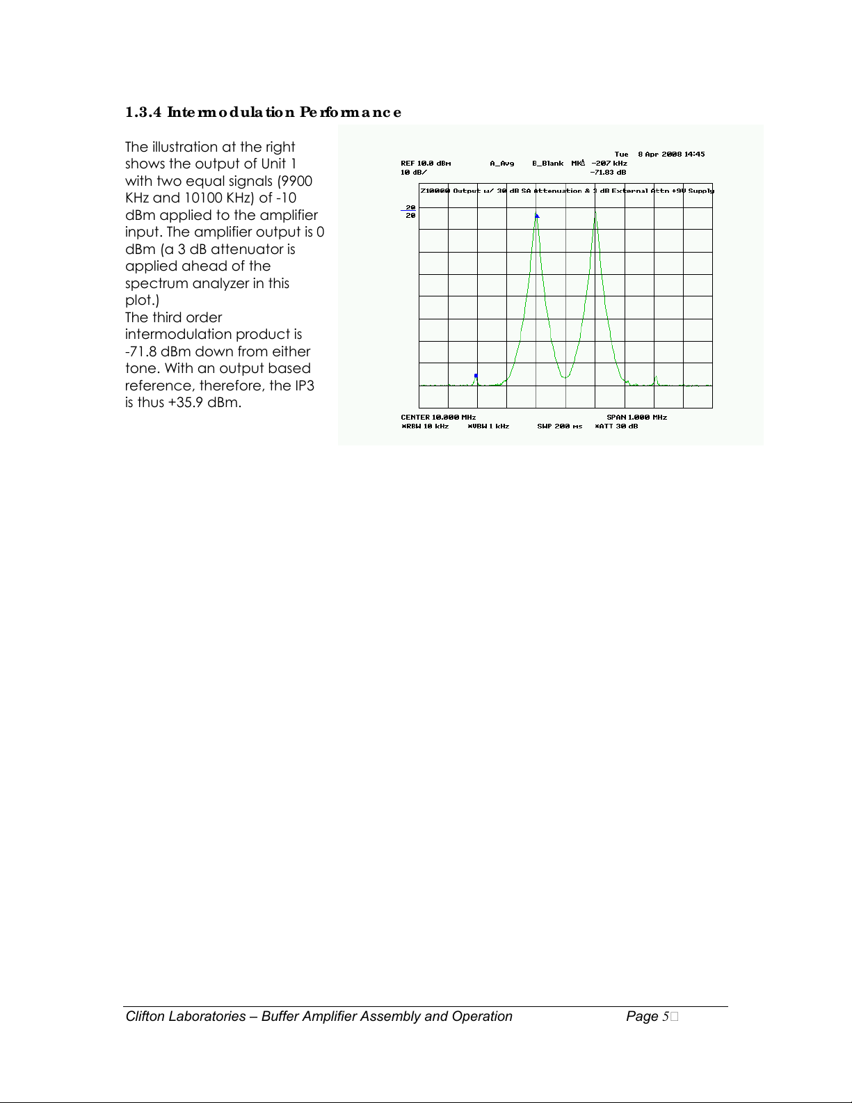
1.3.4 Inte rm o d ula tio n Pe rform a nc e
The illustration at the right
shows the output of Unit 1
with two equal signals (9900
KHz and 10100 KHz) of -10
dBm applied to the amplifier
input. The amplifier output is 0
dBm (a 3 dB attenuator is
applied ahead of the
spectrum analyzer in this
plot.)
The third order
intermodulation product is
-71.8 dBm down from either
tone. With an output based
reference, therefore, the IP3
is thus +35.9 dBm.
Clifton Laboratories – Buffer Amplifier Assembly and Operation Page 5
Page 8
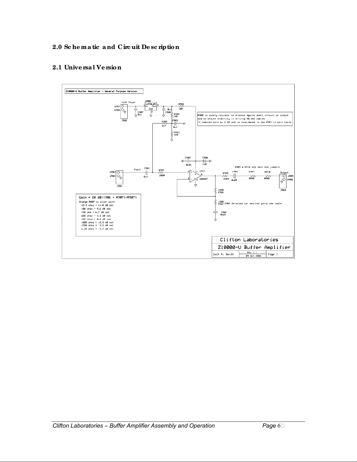
2.0 Sc he m a tic a nd Circ uit De sc riptio n
2.1 Unive rsa l Ve rsio n
Clifton Laboratories – Buffer Amplifier Assembly and Operation Page 6
Page 9

2.2 K2 Ve rsion
2.3 The o ry o f O pe ra tio n
The operational circuitry of both buffer amplifiers is similar, with differences in component
selection for frequency shaping in the K2 version.
2.3.1 Po we r Supply.
The AD8007 amplifier is rated at an absolute maximum operating voltage of 12V. In order
to provide a safety margin, and to decouple the amplifier from the power supply, U902,
a three-terminal fixed regulator, provides a source of stable +9V to U901. C907 and C908
provide additional decoupling. U901, the AD8007 amplifier, obtains its power via the RC
decoupling network comprised of R902, C902 and C906.
Since the circuit operates from a single positive power supply, it is necessary to bias
U901’s input to approximately V/2. This is accomplished by the 2:1 voltage divider chain
of R902/R903. C903 bypasses the V/2 reference voltage; whilst R905 increases U901’s
input impedance by isolating C903’s RF ground. R905’s maximum value is determined by
the U901’s input bias current on the positive pin, specified by Analog Devices as 8μA. For
4.7 KΩ, this bias current represents an IR drop of 38 mV. With a DC gain of 4, the
corresponding output DC offset will be about 150 mV. If absolutely necessary for high
input impedance, R905 may be substituted with a higher value resistor, up to
approximately 22 KΩ. However, at frequencies above a few MHz, the input impedance is
Clifton Laboratories – Buffer Amplifier Assembly and Operation Page 7
Page 10
dominated by shunt capacitance; increasing R905 should be done only with an
understanding of all the factors affecting the input impedance.3
2.3.2 A m p lifie r
U901, an Analog Devices AD8007, is a high performance, low noise c urre nt fe e db a c k
amplifier, with a gain-bandwidth product exceeding 650 MHz. A current feedback
amplifier is also known as a “transimpedance” amplifier. Analog Devices describes how
a current feedback amplifier works:
First, the negative input of a CFA responds to current; the output voltage is
proportional to that current, hence tra nsim p e da nc e (V(o ut) = Z(t) I(in)). Instead of
keeping the negative input current small by maintaining high input impedance,
and using feed-back and voltage gain to keep the input voltage difference
small, the CFA keeps the voltage difference small by virtue of its low input
impedance (like looking back into a low-offset emitter follower); and it keeps its
net input current small dynamically by feedback from the output.
When an ideal CFA is driven at the high-impedance positive input, the negative
input, with its low impedance, follows closely in voltage; and the high gain for
error current and the negative feedback through Rf require that the currents
through Rf and Rin be equal; hence V(o ut) = V(in)[R(f)/R(in) + 1], just like for
voltage-feedback amplifiers. A major difference is that the slew rate can be quite
high, because large transient currents can flow in the input stage to handle rapid
changes in voltage across the compensating capacitor(s). Also, the low
impedance at the negative input means that stray input capacitance will not
substantially affect the amplifier's bandwidth.
U901’s gain (in dB) is determined by the ratio of resistors R906 and R907:
907906
Gain+=
In the Z10000-K2 version, R905 and C901 form a high-pass RC filter and input attenuator.
Adjusting R905 to values below 4.7K will increase the input attenuation, which is desirable
to achieve the desired amplifier gain when used in a K2.
The Z1000-K2’s output stage also uses RC high pass filtering (R908 & C905) to roll off
frequencies below approximately 5.6 MHz. The AD8007’s output is connected through a
five element low pass filter, consisting of L901, L902, C910, C911 and C912. The low pass
filter sharply rolls off frequencies above 7 MHz.
C910, C911 and C912 are removed in the Z10000-U model and L901 and L902 are
replaced by zero ohm jumpers. In addition, C901 is changed in the Z10000-U to 0u1 and
C905 to 0u22 to provide a flat frequency response down into the 50 KHz range.
R908, 49.9 Ω, allows U901 to drive capacitive loads, such as coaxial cable and also
protects U901 against operation into short circuits. However, the voltage divider effect of
log20
10
R
907
RR
3
Clifton Laboratories will provide interested Z10000 owners with the LTSpice model of the
AD8007 and an LTSpice model of the amplifier circuits upon request. SPICE modeling will allow the
user to determine the effects of component changes with a reasonable degree of accuracy.
Clifton Laboratories – Buffer Amplifier Assembly and Operation Page 8
Page 11

R908, which is in series with the load, reduces the net available gain into a 50 ohm load
by 6 dB.
2.3.3 G a in Se tting in the Z10000- U Buffe r Am plifie r
Note: This section applies only to the Z10000-U amplifier. See later discussion for gain
setting of the Z10000-K2 amplifier.
To vary buffer amplifier’s gain, select R907 using the following table or the provided
graph.
Ne t Ga in (ne t o f R9 0 8 se rie s re sista nc e) R907
+15 dB 49.9 Ω
+10 dB 100 Ω
+6.7 dB 150 Ω
+4.3 dB 221 Ω
0 dB 499 Ω
-2.5 dB 1000 Ω
-3.5 dB 1500 Ω
-4.2 dB 2200 Ω
R906 and R901 should not be varied from their design values without a thorough analysis
of the circuit.
The effect of changing R907 upon gain and bandwidth is illustrated in the following plot.
The plot is based upon SPICE simulation of the circuit and is representative of the actual
circuit.
In the –U version, R905 will normally be 4K7Ω.
Clifton Laboratories – Buffer Amplifier Assembly and Operation Page 9
Page 12
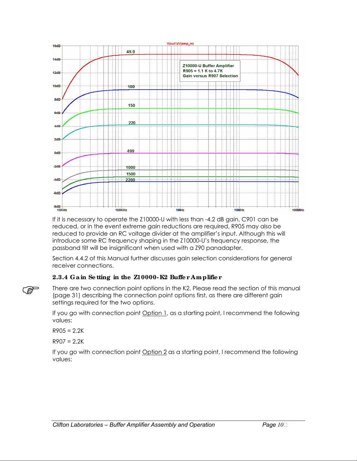
If it is necessary to operate the Z10000-U with less than -4.2 dB gain, C901 can be
reduced, or in the event extreme gain reductions are required, R905 may also be
reduced to provide an RC voltage divider at the amplifier’s input. Although this will
introduce some RC frequency shaping in the Z10000-U’s frequency response, the
passband tilt will be insignificant when used with a Z90 panadapter.
Section 4.4.2 of this Manual further discusses gain selection considerations for general
receiver connections.
2.3.4 G a in Se tting in the Z10000- K2 Buffe r Am p lifie r
There are two connection point options in the K2. Please read the section of this manual
(page 31) describing the connection point options first, as there are different gain
settings required for the two options.
If you go with connection point Option 1, as a starting point, I recommend the following
values:
R905 = 2.2K
R907 = 2.2K
If you go with connection point Option 2
values:
as a starting point, I recommend the following
Clifton Laboratories – Buffer Amplifier Assembly and Operation Page 10
Page 13

R905: 4.7K Ohms
R907: 220 Ohms (this is a starting point; depending on your sound card gain it may be
necessary to reduce R907 to 100 ohms or even 49.9 ohms for increased net gain.)
Note that as the Z10000’s gain is increased, the clipping point of the amplifier decreases.
Larry, N8LP, reports that with R907 at 120 ohms, the clipping point is -5 dBm. Of course, -5
dBm represents an extremely strong signal, unlikely to be encountered in most K2
environments.
If you decide to use connection point Option 1
, gain setting in the K2 version buffer
amplifier is a bit more complex, because the normal operating mode in a K2 transceiver
requires a negative net gain—in other words, a net loss—of about -14 to -15 dB. Part of
4
the negative gain is obtained by intentional rolloff in C901 and R905.
This combination provides a net gain of about -14 dB. This much loss is required because
the recommended K2 connection point has approximately 18 dB net gain from the K2’s
post-mixer amplifier, Q22 (2N5109). The Z90 is designed for optimum signal level when the
5
net gain between the antenna and the Z90’s input is approximately 0 dB.
When
combined with the approximately 3.5 dB loss of the supplied 4.915 MHz bandpass filter,
setting the Z10000-K2’s gain at -14 dB meets the “net zero gain” requirement. (This
computation assumes the K2 is operating in the “normal” mode, i.e ., pre-amp off and
attenuation off.) Don’t worry, by the way, about achieving this “net zero gain” objective
perfectly. A few dB one way or the other is not critical. If you are to err, however, better
results will usually be found if you err on the side of operating the Z10000-K2 with a greater
loss than operating it for higher gain.
Although developed with Clifton Laboratories Z90/91 panadapter, measurements shows
that net 0 dB transfer gain (from K2 antenna input to Z10000 sample output) is an
excellent operating point for the Softrock Lite 6.2 receiver when used as a panadapter or
second receiver. If desired, of course, the Z10000’s gain can be increased as discussed
herein.
The following three figures show the net gain out of the Z10000-K2 as a function of R907
for three values of R905, 4.7K, 2.2K and 1.1K.
4
It would be possible, of course, to dispense with the buffer amplifier completely and
connect the Z90 to the K2’s IF with a resistive matching pad. However, the resistive matching pad
will not provide isolation as does the Z10000-K2. Although the Z90 has relatively low undesired
emissions from its input connector, the extra isolation of the buffer amplifier provides additional
protection against unwanted signals entering the K2’s IF amplifier chain.
5
In other words, a 1 μV signal at the frequency the receiver it tuned to should yield about a
1 μV signal at 4915 KHz into the Z90.
Clifton Laboratories – Buffer Amplifier Assembly and Operation Page 11
Page 14
Clifton Laboratories – Buffer Amplifier Assembly and Operation Page 12
Page 15

3.0 Asse m b ly
3.1 Pa rts List
The Z10000 parts are packaged in a several small envelopes, depending upon the
option purchased.
All Z10000 kits
• Resistors. All surface mount resistors, for both the –U and –K2 versions. [All R]
• Capacitors for the –U version [All C a p]
• Printed circuit board [PC B]
• Semiconductors (AD8007 and 78L09) [Se m i]
K2 Frequency Sensitive Parts
• Capacitors and inductors necessary to shape the amplifier’s frequency
response to peak at 4.9 MHz. [K2 Fre q]
:
Internal Mounting
• Parts associated with mounting the Z10000 (either U or K2) inside a receiver. [Int]
• K2-specific internal connectors are supplied where the purchaser selects the
Internal Mounting option and also the K2 frequency sensitive parts. [K2 C o n]
Clifton Laboratories – Buffer Amplifier Assembly and Operation Page 13
Page 16

If ordering a Z10000-K2, therefore, you will have several extra capacitors and
resistors that are not used in the –K2 version, as all kits are shipped with the full set of
–U parts.
When working with capacitors particularly, do not removed the individual parts
from their color-coded packaging until you are ready to use the component, as
their values are not marked on the part and cannot normally be visually
distinguished. Hence, if you mix up the capacitors, you will have to measure their
values with a capacitance meter.
Also, do not confuse 100 ohm 1% resistors (identified as 1000) with 1.0K ohm 1%
parts, identified as 1001.
Note that the schematic identifies parts with the multiplier as the “decimal” point.
For example a 1K ohm resistor is identified as a 1K0, and a 49.9 ohm resistor as 49R9.
Common Components - K2 and Universal Models
Envelope
Typical Photo Designation Value Marking Number Qty
C902 0u01 Not marked All Cap 1
C903 0u1 Not marked All Cap 1
C904 0u22 Not marked All Cap 1
C906 1u0 Not marked All Cap 1
C907 0u1 Not marked All Cap 1
C908 0u1 Not marked All Cap 1
R901 200R 2000 All R 1
R902 10R 10R0 All R 1
R903 1K0 1001 All R 1
R904 1K0 1001 All R 1
R906 499R 4990 All R 1
R908 49R9 49R9 All R 1
U901 AD8007 AD8007ARZ Semi 1
U902 LM78L09 KA78L09AZ Semi 1
Clifton Laboratories – Buffer Amplifier Assembly and Operation Page 14
Page 17

Envelope
Typical Photo Designation Value Marking Number Qty
Z10000-K2 Only
Z10000-U Only
C901 8p2 Not marked K2 Freq 1
C905 5600pF Not marked K2 Freq 1
C910 1200pF Not marked K2 Freq 1
C911 1200pF Not marked K2 Freq 1
C912 1200pF Not marked K2 Freq 1
L901 1u5 K2 Freq 1
L902 1u5 K2 Freq 1
C901 0u1 Not marked All Cap 1
C905 0u22 Not marked All Cap 1
L901 0 ohm jumper All R
L902 0 ohm jumper All R
Gain Setting Parts - For both Z10000-K2 and Z10000-U
External and Mechanical Parts
See manual to determine proper value
Resistor Supplied for Selection
R905 4K7 4701 All R 1
R905 2K2 2201 All R 1
R905 1K1 1101 All R 1
Resistor Supplied for Selection
R907 49R9 49R9 All R 1
R907 100R 1000 All R 1
R907 150R 1500 All R 1
R907 220R 2200 All R 1
R907 499R 4990 All R 1
R907 1K0 1001 All R 1
R907 1K5 1501 All R 1
R907 2K2 2201 All R 1
Clifton Laboratories – Buffer Amplifier Assembly and Operation Page 15
Page 18
Both Z10000-K2 and Z10000-U
Z10000-01 RG178 2 ft INT
Z10000-02 Bulkhead Connector INT
Z10000-03 6" red wire INT
Z10000-04 1/2" MF 4-40 standoff INT
Z10000-12 fish paper INT
Z10000-08 Printed circuit board
Z10000-10 4-40x1/4" machine screw INT
Z10000-11 4-40 hex nut INT
Z10000-12 3/32" x .5" red heat shrink tubing INT
Z10000-13 3/32" x .5" black heat shrink tubing INT
Z10000-14 3/32" x .5 green heat shrink tubing INT
Z10000-16 3/16" x 2" heat shrink tubing INT
Z10000-K2 Only
Z10000-05 8-pin female header All R
Z10000-06 3-pin female header All R
Z10000-07 3-pin male header All R
Multiple part values are provided for R905 and R907, to be selected by the builder as
discussed in the text.
Printed instructions are not supplied; this manual is to be downloaded from the Clifton
Laboratories web site.
Heat shrink tubing supplied may differ in diameter, length and color from the values in
the above parts table.
3.2 Wo rking with Surfa c e Mo unt C o m po ne nts
If you are unfamiliar with installing surface mount components, you should review this
section of the Assembly Manual. The surface mount components in this kit are
considered “large” by industry standards, and should not represent difficulty if you have
prior kit assembly experience, either surface mount or through-hole.
3.2.1 To o ls
I use the following tools in assembling surface mount printed circuit boards:
To o l C o m m e nts Appro xima te
C o st
I use curved nose forceps
to hold parts while
soldering. I prefer the
pattern 7-SA forceps with
gently curved tips, but the
angular pattern 6-SA may
be preferred by some.
These are by Technik and
are non-magnetic stainless
$9.00 each MSC part
Sourc e
number:
7-SA
pattern:
88348099
6-SA
pattern:
88348081
Clifton Laboratories – Buffer Amplifier Assembly and Operation Page 16
Page 19

To o l C o m m e nts Appro xima te
C o st
Sourc e
steel.
I find clip-on magnifiers
essential to view small
parts. I keep both 1.75 x
and 3.5 x magnification
types at hand.
The 3.5 x magnifiers have a
$20 each MSC part
numbers:
1.75X:
06533202
3.5X:
06533236
working distance of 4”, so
it gets you “up close and
personal” with the parts!
(I’m not a fan of the
headband style
magnifiers, but personal
tastes differ in this regard.)
Of course, if you don’t
wear glasses, a different
style magnifier will be in
order.
Small diameter solder is
essential. I use either 0.015”
diameter or 0.022”
diameter solder. If you can
find it, I find solder with a
$15 for ½
pound
Kester
Mouser
part
number
533-23-
6337-07
slight amount of silver (3%
typically) produces a
better appearing joint.
My 0.015” solder is Kester
“44 rosin, 63/37 eutectic
mixture. My 0.022” solder is
(believe it or not) Radio
Shack 62/36/2, with 2%
silver.
If the pad being soldered
to is at all tarnished, a
touch of solder flux will
clean it up. Some like to
$4 Mouser
part
number:
533-0951
use flux regardless of the
pad condition. I prefer a
pen-type dispenser.
Clifton Laboratories – Buffer Amplifier Assembly and Operation Page 17
Page 20

To o l C o m m e nts Appro xima te
C o st
Solder wick can’t be beat
for cleaning up unwanted
solder, or for removing
solder from a pad after a
part is changed. For small
surface mount parts, I like
narrow solder wick, 0.025
to 0.030.”
Finally, you need
something to hold the PCB
in place whilst you work on
it.
I use a Panavise #301 (with
nylon jaws) for small
boards and a Panavise
#324 board holder for
larger projects.
$2.50 Mouser
$45 for the
standard
Panavise
$85 for the
PCB holder
Sourc e
part
number:
5878-80-1-
5
#324 PCB
Holder is
Mouser PN:
591-324
#301
Standard
Panavise is
Mouser PN:
591-301
Mo use r: http://www.mouser.com/ (excellent line of electronic parts and no
minimum order size)
http://www1.mscdirect.com/ (Tools of variety almost unimaginable and it’s
MSC:
all in stock. No minimum order, prices may be a bit on the high side, but I’ve never
bought a tool from them that I’ve been disappointed in. Their customer service is among
the best I’ve seen.)
The tool not
quite useful for many purposes around the electronics
workbench, but when it comes to holding surface mount
parts, I’ve found them to excel at being “parts
launchers” with the ability to shoot a small surface mount
component across the room in an instant.
This tools list assumes you have a suitable soldering iron. I
use two Hakko 936 soldering stations. For integrated
Clifton Laboratories – Buffer Amplifier Assembly and Operation Page 18
to use—self-closing forceps. These tools are
Page 21

circuits such as U801/U901, I use a 0.032” diameter long taper conical tip. For larger
surface mount and through-hole parts, I use a 1/8” screwdriver tip. My experience is that
a lower power soldering iron isn’t adequate, and one of much greater power is too
much. Whether this is a true Goldilocks optimum or just my personal preference remains
to be determined.
If you are thinking of purchasing a new soldering station, I recommend the Hakko Model
936.
3.2.2 Installing Surfac e Mo unt C o m po ne nts
3.2.2.1 Inte gra te d C irc uits
U901 is a reasonably easy to install surface mount IC, if you have the correct tools and
follow a few simple steps.
Before starting, remember to apply proper anti-static procedures. Study the IC’s
marking and the PCB layout so that you know the correct orientation.
The idea is to hold the IC in place by soldering two diagonal corners in place and
then solder the remaining pins. Start by applying a sparing
one of the corner pads. Then apply a similar amount of solder to the diagonal
corner pad. Place the IC on the PCB, correctly oriented, with pins centered on
the pads. While holding
the IC in place, touch the
soldering iron to the first
tinned pad, tacking the
IC’s pin in place. The
small figure shows an
AD8007 after the
diagonal pins have been
tack soldered in place.
Note how the pins are
centered over the PCB
pads.
Check the orientation of the IC, verifying that it
is properly centered over the pads. If you don’t
get this right now, it will be far more difficult to
correct when the second pin is soldered in
place. When you are satisfied that the IC is
centered on its pads, touch the other diagonal
tinned pad with your soldering iron.
amount of solder on
Double check that the IC has not shifted during
the earlier steps and that the IC’s pins are
centered on their respective pads. Then solder
the remaining pins to their pads. Depending on
how the PCB was constructed, it may have sufficient solder plating so that
additional solder is unnecessary—simply touching the soldering iron to the pin and
pad flows enough solder to form a reliable joint. If this isn’t
possible with your PCB, then apply a small
form the joint.
After each time you touch the solder to the soldering iron,
check the end of the solder for a blob or ball. If you find the
solder has formed a ball, cut it off at an angle to form a
Clifton Laboratories – Buffer Amplifier Assembly and Operation Page 19
amount of solder to
Page 22

pointed end. Otherwise, it will be difficult to control the amount of solder
deposited.
After soldering, check for bridged pins or shorts to ground. Clean up any
problems with solder wick.
3.2.2.2 Passive Co mp o ne nts
To install a passive component,
use a similar approach:
Lightly tin one pad.
With angled forceps (or
your favorite tool) hold
the part in place and
solder the part to the
tinned pad with a light
touch of the soldering
iron. This will anchor the
part in place. Notice how
nicely Technik pattern 7A
forceps hold the part in
place without obscuring
vision or blocking the
soldering iron.
Solder the remaining
pad(s). If necessary
rework the first pad
connection.
It does not take a large amount of solder to properly attach a surface mount
component. A correctly installed part will be flush against the board and have a small
filet at the end caps.
3.2.3 Re mo ving De fe c tive Pa rts
In almost every instance, trying to salvage a surface mount part installed wrong is a
waste of time. A 1% 1206 size surface mount resistor, for example, costs about 2 cents in
100 lots. It’s much easer to use a pair of cutters and snip the part in half. (Resistors and
capacitors are ceramic based—they shatter when cut.)Then use solder wick to remove
the two halves. Clean up the pads with additional applications of solder wick.
To remove a multi-pin IC, a similar approach can be used—carefully cut the part into
pieces with cutters, exercising care to avoid damaging traces or the PCB. A hot air gun
can also be used to simultaneously liquefy the solder at all IC pins. The IC can then be
lifted free of the PCB. Care must be taken, of course, to avoid damaging nearby parts
with the heat gun.
An alternative IC removal approach is ChipQuik (DigiKey PN SMD1-ND, approximate
price $15). ChipQuik’s kit includes special flux and a low temperature melting point solder
that mixes with the normal solder and allows the chip to be removed without extensive
heating.
Because I do so much surface mount work, I’ve purchased a Hakko 950 SMT tweezer
handpiece and several blades. Although not cheap, it’s an excellent tool, like all other
Hakko products I’ve purchased.
Clifton Laboratories – Buffer Amplifier Assembly and Operation Page 20
Page 23

3.2.4 Mo st c omm o n e rro r
The most common error I make in installing a surface mount resistor or capacitor is to not
center the part on the pads, resulting in the metalized end of the component shorting to
ground, where it bridges the pad’s isolation. This error can be completely avoided by
carefully centering the part and holding it in the correct position whilst soldering one end.
It’s much easier to fix this type of error before soldering the second end!
With integrated circuits, the most common error is to bridge solder across adjacent pins.
In most cases, applying solder wick will remove the bridge and leave the pins correctly
soldered in place.
3.2.5 Te flon C o a x
The coaxial cable supplied with this kit is RG178, with Teflon outer jacket and center
insulation. Teflon will not melt during normal soldering operations, unlike, for example,
RG174, with a center conductor insulation that melts if you look at it crossways. However,
RG178 requires some special handling:
Most wire strippers do not work well with Teflon. I use a Hakko FT800 thermal wire
stripper. Before acquiring the FT800, I used either a special micrometer-type wire
stripper or an X-Acto knife. It is extremely easy to cut through the shield or the
center condutor when stripping the coax, so apply light pressure when cutting.
RG178 is small (about 0.078” [1.8mm] diameter) so be careful when stripping it.
The shield is comprised of #38 AWG wire, which is tiny. It’s easy to wind up with
small pieces of shield in places where you don’t want them, so look over your
work with a magifying glass for stray bits of shield.
Likewise, the center conductor is #30 AWG and it’s very easy to cut through it
when stripping the center insulation.
Gently does it when using the X-Acto knife. Let the sharpness of the blade do the
work, and do not apply more than the absolute minimum pressure necessary.
You might practice stripping the jacket and center conductor on the free end of
the cable to get a feel for how easy or difficult it will be for you before doing it
“for real.”
Cutting the cable with a bit of excess length is not a bad idea as it may save you
from redoing a lot of work if your first attempt at stripping the cable fails.
You have only one opportunity to cut the connector end of the cable. The old
carpenter’s rule of “measure twice, cut once” applies with force here. Replacement
cables are $15 from Clifton Laboratories.
After soldering the RG178 to the input and output printed circuit board pads, be careful
not to apply excessive mechanical force to the cables. It’s easy to rip the pad off the
printed circuit board or break the cable where it is soldered. It’s also easy to wind up
with a stray wire from the shield floating around and shorting the input and output pads.
Any stray bits of shield wire should be carefully removed.
Clifton Laboratories – Buffer Amplifier Assembly and Operation Page 21
Page 24

4.0 A sse m b ly
4.1 Co m po ne nt Pla c em e nt
Locate the appropriate PCB and orient yourself with the board. Identify the top and
bottom. The top has silk screening as well as solder masking.
The photograph shows an earlier version of the PCB. Later PCBs correct the silk screen
error identifying R907 as R8
production circuit boards may be slightly smaller than in the photographs.
This photograph shows parts placements for both the -K2 and -U versions of the Z10000.
Clifton Laboratories – Buffer Amplifier Assembly and Operation Page 22
07, and slightly rearrange other silk screen legends. In addition,
Page 25

The bottom PCB surface is solder masked but not silk screened. Please use the following
annotated photograph for parts placement.
The photograph below shows the parts placement for the -K2 version and, with respect
to C902, C906, C907 and C908, the -U version as well.
Clifton Laboratories – Buffer Amplifier Assembly and Operation Page 23
Page 26

The Z10000-U differs on the bottom assembly in several respects from the -K2 version:
Low pass filter capacitors C910, C911 and C912 are not used.
L901 and L902 are not used. Instead, 000 ohm jumpers are installed in their place.
The photograph shows the most recent (2008) PCB board. C906 in the photograph is a
tantalum electrolytic capacitor. Normally a ceramic capacitor is supplied with the
Z10000, although a tantalum electrolytic may be provided in some instances.
Clifton Laboratories – Buffer Amplifier Assembly and Operation Page 24
Page 27

The assembled Z10000 top view photo below is identical in appearance for both the -U
and -K2 models, as the differences are only in component values.
The board shown uses plug-in headers for test purposes. Your board will normally use
direct wire connections to the power, input and output pads, although you are, of
course, free to use header pins if so desired.
The photo below shows the bottom view of an assembled Z10000-U.
Clifton Laboratories – Buffer Amplifier Assembly and Operation Page 25
Page 28

4.2 Co m po ne nt Insta lla tio n
The assembly instructions are almost identical for both the K2 and Universal board. Where
appropriate, the following instructions will identify the differences.
Before starting construction, it is necessary to select the gain programming resistor (R907)
and the input resistor (R905). In the case of an Elecraft K2 transceiver and Option 1
connection point, the recommended values are R905=2.2K, R907=2.2K For Option 2
connection, the starting point should be R905=4.7K, R907=220 ohms. For assistance in
determining the programming resistor value read Sections 2.3.3, 2.3.4 and 4.4.2 of this
document.
If the internal installation option is purchased, locate the fish paper6 (black, stiff
paper) and the printed circuit board. Align the 1/8” hole in the fish paper with the
PCB’s mounting hole and trim the fish paper to approximately the same size as
the buffer amplifier PCB using scissors or an X-Acto knife. Return the fish paper to
a safe location.
Now the surface mount parts on the top are installed:
[Se m ic o nd uc tor Pa c kag e ] Install U901 (AD8007) using the technique discussed
earlier.
[K2 Fre q –K2; All C a p for - U] Install C901 (0.1 uF for –U; 8.2pF for –K2, both
unmarked)
[A ll C a p] Install C903 (0.1 µF, unmarked)
[A ll C a p] Install C904 (0.22 µF, unmarked)
[A ll R] Install R901 (200 Ω, marked 2000)
[A ll R] Install R902 (10 Ω, marked 10R0)
[A ll R] Install R903 (1 KΩ, marked 1001)
[A ll R] Install R904 (1 KΩ, marked 1001)
[A ll R] Install R906 (499 Ω, marked 4990)
[A ll R] Install R908 (49.9 Ω, marked 49R9)
[K2 Fre q fo r – K2; All Ca p for - U] Install C905 (5600 pF for –K2; 0.22 µF for -U, both
unmarked)
[Se le c t R9 05 fro m [A ll R] following instruc tio ns a t Sec tio ns 2 .3.3, 2 .3.4 a nd 4.4 .2 ]
Install R905
[Se le c t R9 07 fro m [A ll R] following instruc tio ns a t Sec tio ns 2 .3.3, 2 .3.4 a nd 4.4 .2 ]
Install R907
Flip the board upside down and install the remaining surface mount components:
[A ll C a p] Install C902 (0.01 µF, unmarked)
[A ll C a p] Install C906. (1.0 µF, unmarked)
[A ll C a p] Install C907 0.1 µF, unmarked)
[A ll C a p] Install C908 (0.1 µF, unmarked)
If you are building the –K2 version, install the frequency-sensitive parts [these parts are not
included with the –U version]:
[K2 Fre q] Install L901 (1u5 inductor)
6
Why this is called “fish paper” remains a mystery. The best I can find is a conversation with
a ham in his 70’s (K8AQC) said that when he was a young man, the old time electricians called it
“fish oil paper” which leads him to believe that the insulating paper at the time was coated with
fish oil, and then heated and rolled. That’s the most plausible explanation I’ve heard for the name.
Clifton Laboratories – Buffer Amplifier Assembly and Operation Page 26
Page 29

[K2 Fre q] Install L902 (1u5 inductor)
You may find the two inductors a bit more difficult to install than the resistors or
capacitors due to the way the leads are formed. After soldering one end in place, check
the associated pads for an inadvertent short circuit to ground. Both pads associated with
each inductor should be an open circuit to ground when checked with an ohmmeter.
Repeat the ohmmeter check after soldering the second end of each inductor.
[K2 Fre q] Install C910. (1200pF, unmarked)
[K2 Fre q] Install C911 1200pF, unmarked)
[K2 Fre q] Install C912 (1200pF, unmarked)
If you are building the –U version, install the filter bypass parts:
[A ll R] Install L901 bypass (Zero-ohm jumper)
[A ll R] Install L902 bypass (Zero-ohm jumper)
The two zero-ohm jumpers are slightly small for the pad spacing but will work if you
carefully center the parts on the pads. After soldering one end of each zero ohm jumper
in place, check for an inadvertent short to ground. Both ends of both pads should be
open circuit to ground when measured with an ohmmeter. Check again after soldering
the second end of each zero ohm jumper.
For all versions:
Now install the remaining through-hole parts:
[Se m i] Install U902. This is a 78L09 3-terminal regulator in a TO-92 package. Note
the orientation of the device as shown in the silk screen outline. You will have to
form the leads to fit the hole. Assess how much vertical clearance is needed
above the PCB. In the –K2 version, press U902 into place so that the body is
approximately 1/8” (3mm) from the top of the PCB. If necessary to have a lower
profile in your particular installation, you may leave the leads longer and bend
the regulator as necessary, avoiding, of course, shorting the leads together.
Otherwise, follow the –K2 installation practice.
The Z10000 is supplied with a length of RG178 coaxial cable with an attached cable jack
bulkhead connector. This cable is to be cut as necessary for your installation, with the
connector on the output and the remaining cable to be for the input connection.
Clifton Laboratories offers an optional 3’ RG174 cable with a male SMA connector on
one end and a male BNC connector on the other end. This cable is not part of the
Z10000 buffer amplifier kit.
Since the Z10000-U may be employed in a variety of receivers or transceivers, explicit
installation instructions cannot be provided. Clifton Laboratories suggests the K2
installation guidelines provided below be used to develop your own installation strategy.
For installation in a K2, prepare the supplied coaxial cable and power hookup wire as
follows.
Exa m ine yo ur K2:
Before cutting the coaxial cable, remove the cover on your K2 and determine where
you wish to mount the SMA bulkhead output connector. Study the photographs in this
manual to understand where the buffer amplifier will be mounted. In a normal
installation, it will be placed next to the noise blanker board, or the place where the
noise blanker board would be installed if your K2 has that option.
Clifton Laboratories – Buffer Amplifier Assembly and Operation Page 27
Page 30

The following photograph shows the normal K2 installation location. The buffer amplifier
mounts on a ½” (12.6 mm) male-female aluminum standoff that replaces one of the
screws holding the K2 main board in place.
Now that you know where the buffer amplifier will be located, determine where the
output SMA connector will be installed.
My K2 has the optional KPA100 100 watt output stage but does not have the K60XV 60
meter band / transverter board. This leaves two open holes (XVTR IN and XVTR OUT) in my
K2, which are the correct size for the SMA bulkhead connector:
Clifton Laboratories – Buffer Amplifier Assembly and Operation Page 28
Page 31

Note that the RCV. ANT. hole is a bit large to properly hold the SMA connector.
If you need to punch or drill a hole in your K2 for the SMA connector, the connector
nominal outer diameter is ¼” (6.4mm). Both nuts require a 5/16” wrench.
Using the cable or a piece of string, determine the cable length required from the SMA
connector mounting position to the buffer amplifier board. In my K2, the length of
required output cable is approximately 6” (152 mm), but yours may vary, and you may
also wish to route the cable differently than I did.
This is a critical dimension, in that if cut too short, you will require a replacement cable.
After cutting the cable, reserve the cut-off piece for the input connection.
Now, determine the length of cable required for the input connection. In the K2,
assuming the Z10000-K2 is installed in the normal location, the input coaxial cable will be
approximately 5 inches (125 mm) long. You should determine if this length is adequate
for your installation and preferred routing.
After you have determined the correct input cable length, cut a section of RG178 to that
length.
Bob, K7HBG, has provided the following drawing showing where he located the SMA
bulkhead in his K2, which is equipped with all possible options and hence has no unused
holes.
Clifton Laboratories – Buffer Amplifier Assembly and Operation Page 29
Page 32

Bob notes that the 6mm (¼”) (internal diameter) lock washer just fits in between the "D"
chassis bracket and the 160 Meter board so it is necessary to carefully measure the hole’s
location.
Bob’s K2 with the
buffer amplifier in
place. Note the
SMA connector
mounting in the
space between the
160 meter board
and the edge of
the back panel.
Clifton Laboratories – Buffer Amplifier Assembly and Operation Page 30
Page 33

The SMA bulkhead connector is supplied with one lockwasher intended to be used on
the outside of the enclosure, between the nut and panel. Bob suggests using a second
internal tooth lockwasher on the inside. If you follow this suggestion, a ¼” (6mm) internal
tooth lockwasher can be obtained at any hardware store.
K2 C o nne c tio n O ptio ns
O ptio n 1
The Z10000-K2 was originally developed and tested with the connection point shown in
the schematic below. This connection point has two advantages and one
disadvantage:
Advantages:
• Connects at a low impedance point, and takes advantage of the K2’s low noise
• Allows use of a 3-pin plug connector that minimizes modifications to the K2 and
Disadvantage:
• The K2’s BFO leakage backwards through the IF chain places an unwanted “pip”
post-mixer amplifier, Q22.
allows easy removal of the Z10000-U for maintenance, if necessary.
in the spectrum analyzer. (See section 4.6 of this manual for a discussion of why
the K2 has BFO leakage.)
Clifton Laboratories – Buffer Amplifier Assembly and Operation Page 31
Page 34

O ptio n 2
Larry, N8LP, has developed an alternative connection option; take the IF sample at R80,
Q22’s 680 ohm base resistor.
This connection point also has advantages and disadvantages:
Advantages:
• Reduced BFO leakage back into the panadapter. This is because the BFO
Disadvantages:
• Less gain from the K2’s low noise post-mixer amplifier. This will reduce the overall
• Requires soldering to the PCB parts and is not as easily reversible as Option 1,
To illustrate the difference in BFO leakage, Larry has supplied three screen images
captured with an LP-PAN panadapter and the Z10000-K2 buffer amplifier connected at
Option 1 and Option 2 points.
With the K2’ s Pre a m p O FF
Clifton Laboratories – Buffer Amplifier Assembly and Operation Page 32
leakage is reduced by the post-mixer amplifier’s isolation, which is around 30 dB.
usable sensitivity of the K2/panadapter combination. On most bands, and with
most antennas, when used with the LP-PAN, this reduction in sensitivity will likely
not prove significant.
Page 35

With the K2’ s Pre - a mp ON
The images show a significant reduction in BFO leakage, on the order of 30 dB.
When the K2’s pre-amp is off, the noise floor is higher, by around 10 dB. This is because
the low noise post-mixer amplifier gain is not available in Option 2. Larry has increased
the Z10000-K2’s gain slightly to offset part of the loss of the post-mixer amplifier gain, but
the Z10000-K2 is optimized for isolation, not noise figure. Hence the composite noise figure
of K2, Z10000-K2 and LP-PAN is not as good under Option 2. However, operating the K2
with its internal pre-amp on significantly improves the composite noise floor of the
K2/Z10000/LP-PAN combination.
Clifton Laboratories – Buffer Amplifier Assembly and Operation Page 33
Page 36

In Option 2, Larry recommends building the Z10000-K2 with the following gain setting
resistor values:
R905: 4.7K Ohms
R907: 220 Ohms (this is a starting point; depending on your sound card gain it may be
necessary to reduce R907 to 100 ohms or even 49.9 ohms for increased net gain.)
Note that as the Z10000’s gain is increased, the clipping point of the amplifier decreases.
Larry reports that with R907 at 120 ohms, the clipping point is -5 dBm. Of course, -5 dBm
represents an extremely strong signal, unlikely to be encountered in most K2
environments.
Use these values only if you use Option 2; do not use these values if you connect using
Option 1.
Each connection option is separately described.
Clifton Laboratories – Buffer Amplifier Assembly and Operation Page 34
Page 37

Inp ut Co nne c tions for O p tion 1
No te : The pho tog ra phs show RG 174 c a b le , no t the RG 1 78 c a b le sup p lie d . The stripping
dim e nsio ns a nd installa tion instruc tio ns re ma in the sa m e .
Strip the outer jacket back about ½”
(12 mm) using an X-Acto or sharp
hobby knife, being careful not to nick
the braid. See Section 3.2.5
concerning working with Teflon cable.
Slip the center conductor through the
braid and form a pigtail as illustrated.
Strip approximately 1/8” (3 mm) from
the center conductor and lightly tin
the bare wire.
Lightly tin the end of the braid to a
length of about 1/8” (3 mm)
Locate the 3-pin male header plug in
Envelope 13. [supplied only with the –
K2 version]
Lightly tin the short side pins. (This is a
good use for the locking forceps, by
the way!)
Clifton Laboratories – Buffer Amplifier Assembly and Operation Page 35
Page 38

Locate the length of green small
diameter heat tubing in Envelope 11
and slip it over the center conductor.
It may be necessary to trim the heat
shrink tubing.
Solder the center conductor to one of
the outside pins of the 3-pin male
header plug.
Slide the heat shrink tubing to be flush
with the header plug plastic base and
apply heat to the tubing to shrink it
into place.
[note – colors changed after photos
taken]
Locate the length of black heat shrink
tubing in Envelope 11 and slip it over
the stripped and twisted braid. Trim
the tubing’s length to fit.
Solder the braid to the center pin of
the 3-pin male header plug.
Slide the heat shrink tubing to be flush
with the header plug plastic base and
apply heat to the tubing to shrink it
into place. Don’t worry if some of the
braid near the jacket is still exposed.
[note – colors changed after photos
taken]
Strip approximately 1/8” from the red
hookup wire and lightly tin it. Solder
the tinned end to the remaining pin of
the 3-pin male header plug.
Locate the length of red heat shrink
tubing in Envelope 11. Slide the heat
shrink tubing over the red wire to be
flush with the header plug plastic base
and apply heat to the tubing to shrink
it into place.
[note – colors changed after photos
taken]
Clifton Laboratories – Buffer Amplifier Assembly and Operation Page 36
Page 39

Locate the length of larger diameter
heat shrink tubing in Envelope 11. It
may be of any color.
Cut a length of about 1” (25 mm) and
slip it over the coaxial cable and
hookup wire, sliding it down to the
plug end. Ensure that the braid is
completely covered by tubing.
The connector end of the assembly
should resemble the photograph, with
no bare shield showing.
Apply heat to shrink the tubing.
Cut short lengths of the remaining
large diameter tubing and apply to
form the coaxial cable and hook up
wire into a cable assembly. Leave the
last 2” (50 mm) free.
Strip the free end of the coaxial cable
to a length of about 3/16” to ¼”
(4.5mm to 6mm)
Remove the center conductor
insulation for about 1/16” (1.5mm).
Prepare the braid as shown in the
illustration.
Strip the free end of the hook-up wire
to a length of about 3/16” (4.5mm).
The photograph shows RG178.
Clifton Laboratories – Buffer Amplifier Assembly and Operation Page 37
Page 40

Route the connections on the top of
the PCB as shown in the photograph.
Solder the hookup wire to the +V side
of J902, i.e ., the non-grounded side of
J902.
Solder the coaxial cable center
conductor to the non-ground side of
J901. Solder the coaxial cable shield
to the grounded pad at J901,
trimming its length if necessary to
ensure that the braid does not cause
a short circuit to the input or any other
component. Check the center
conductor resistance to ground with
an ohmmeter. It should read as an
open circuit.
Inp ut Co nne c tions for O p tion 2
Note: Since Option 2 results in hard wiring the Z10000 to connection points in the K2,
before making the connections described below, follow the check out procedures
described in Section 4.3 of the manual.
Cut a length of the coaxial cable
approximately six inches (150 mm)
long. Strip both ends of this piece of
coaxial cable to expose
approximately 0.5” (12 mm) of the
center conductor. Solder it to J903;
the ground shield to the ground
connector of J903 and the center
conductor to the non-grounded pad.
Route the connections on the bottom
of the PCB as shown in the
photograph.
Strip 0.25 inches (6 mm) from both
ends of the short length of red hookup
wire. Solder the hookup wire to the +V
side of J902, i.e ., the non-grounded
side of J902.
Strip the free end of the long coaxial
cable with the SMA connector to
expose 0.5” (12 mm) of the center
conductor. Solder the coaxial cable
Clifton Laboratories – Buffer Amplifier Assembly and Operation Page 38
Page 41

center conductor to the non-ground
side of J901. Solder the coaxial cable
shield to the grounded pad at J901,
trimming its length if necessary to
ensure that the braid does not cause
a short circuit to the input or any other
component. Check the center
conductor resistance to ground with
an ohmmeter. It should read as an
open circuit.
Connect the free end of the short
coaxial cable to R80. The shield
goes to the ground side of R80,
and the center conductor to the
base pin side of R80, as illustrated
in the photograph to the right.
Connect the red hookup wire as
illustrated.
O utput Co nne c tion Unde r O p tio n 1
If you have not already done so,
locate the length of coaxial cable
with the SMA bulkhead connector
and cut it to the length you have
determined, following the earlier
instructions.
Clifton Laboratories – Buffer Amplifier Assembly and Operation Page 39
Page 42

Strip the free end of the coaxial
cable to a length of about 3/16”
to ¼” (4.5mm to 6mm)
Remove the center conductor
insulation for about 1/16” (1.5mm).
Prepare the braid as shown in the
illustration.
The photograph shows RG178.
Solder the coaxial cable center
conductor to the ungrounded
pad at J903.
Solder the coaxial cable shield to
the grounded pad at J903,
trimming its length if necessary to
ensure that the braid does not
cause a short circuit to the input or
any other component. Check the
center conductor resistance to
ground with an ohmmeter. It
should read as an open circuit.
At this point, your completed
buffer amplifier should resemble
the photograph.
4.3 Che c ko ut
Note: If you are following Option 1, the Z10000 is a free standing board, with plug-in
connections. If you follow Option 2, the board is hard wired into the K2. In this case,
these measurements should be made before soldering the Z10000-K2 into the K2.
Before applying power, make the following resistance checks. The data presented is
taken with a Fluke 189 digital multi-meter and different meters may provide differing
readings. However, any significant variance from these values should be investigated
for potential problems. The negative meter lead should be connected to a ground
point on the Buffer Amplifier PCB. The test point (TP) Key numbers are depicted in the
photograph below.
Me asuring Point TP Ke y Re ading C o m m e nts
J902 (+12 V input)
Clifton Laboratories – Buffer Amplifier Assembly and Operation Page 40
1
2.5 K This value may vary considerably from
Page 43

Me asuring Point TP Ke y Re ading C o m m e nts
ohmmeter to ohmmeter.
J901 input pad
J903 output pad
U901, pin 7 (Vcc)
U901, pin 6 (output)
U901, pin 4
(ground)
U901, pin 3 (+
input)
U901, pin 2 (- input)
2
3
4
5
6
7
8
infinite Should be infinite to ground as DC is
blocked by C901
infinite Should be infinite to ground as DC is
blocked by C905.
2.0 KΩ Reading dominated by R903/904
voltage divider impedance.
5 MΩ Should be high impedance; hundreds
of KΩ at least.
0 Ω
5.9 KΩ This value may vary considerably from
ohmmeter to ohmmeter.
5 MΩ Should be high impedance; hundreds
of KΩ at least.
If the Buffer Amplifier meets these measurements, apply +12 V DC to the power input,
with the negative return to the PCB ground. Measure the input current. It should be
approximately 20 mA, and readings significantly over this value should be
investigated.
Clifton Laboratories – Buffer Amplifier Assembly and Operation Page 41
Page 44

4.4 Insta lling the b uffe r a m p lifie r
This section discusses installing the Buffer Amplifier in the K2 and other receivers and
transceivers. Although specific detail is provided regarding the K2, installation in other
equipment is up to the user, following the guidelines in this document.
Note: Although I’ve made the Buffer Amplifier installation as “no holes” as possible, you
may find it necessary to add a small hole to fit the SMA connector to the K2’s back panel
for the signal output.
4.4.1 Ele c ra ft K2 Tra nsc eive r- O p tio n 1
The K2 connection concept following Option 1 is illustrated in the following figure.
Clifton Laboratories – Buffer Amplifier Assembly and Operation Page 42
Page 45

Elecraft has conveniently provided the three connections the Buffer Amplifier needs
(signal sample, ground and +12 V) at J12, the noise blanker connection socket, on three
consecutive pins, no less. The following sections describe how the Buffer Amplifier is
connected and installed, whether the noise blanker board is present or not. The Buffer
Amplifier, if installed as described, will not interfere with the noise blanker’s operation,
should it be installed.
If your K2 does not
the steps described at Section 4.4.1.1.
have the optional noise blanker board installed, please first complete
4.4.1.1 Units without the O p tio na l No ise Bla nke r Boa rd
Locate the 8-pin female header socket provided with the K2 Buffer Board kit in Envelope
13. This socket will be installed at position J12 in the K2’s RF board. These installation steps
mimic Elecraft’s noise blanker installation instructions, except for those steps associated
with the noise blanker itself.
Turn the K2 off and disconnect the power (either external supply or internal
battery)
Remove the top and bottom covers, but not the heat sink panel.
Install the 8-pin female header socket on the RF board at location J12. Do not
solder it in place yet; just mechanically install it from the top of the RF board.
Solder one pin near the middle of the connector. It’s important that the
connector seats firmly against the PCB, so apply down pressure on it whilst
soldering the pin. If the socket is not flush with the PCB, reheat the pin whilst
applying downward pressure. Make sure the socket is not tilted up on one end or
the other, but contacts the PCB for its full length.
Clifton Laboratories – Buffer Amplifier Assembly and Operation Page 43
Page 46

Do not make any other changes in your K2. If you later purchase the noise
blanker board, it will not be necessary to remove the 8-pin socket, as it is identical
with the socket installed in connection with the noise blanker board. (Of course,
the other changes to the RF board required for the noise blanker installation will
be necessary at that time.)
Follow the installation instructions as for rigs with the noise blanker board, except
that the 3-pin male header plugs directly into the newly installed 8-pin socket at
J12. Pin 1 of the 3-pin header plug goes to Pin 1 of the 8-pin socket at J12.
4.4.1.2 Units with the O p tio na l No ise Bla nke r Bo a rd
Turn the K2 off and disconnect the power (either external supply or internal
battery)
Remove the top and bottom covers, but not the heat sink panel.
Remove the noise blanker board by removing the 4-40 screw from the stand-off
and unplug the noise blanker board.
Turn the noise blanker board upside
down and locate the 8-pin male
header, P1.
The re is no d e finitive wa y to install the thre e - plac e fe m a le he ade r so c ke t onto the no ise
blanke r PC B. Two wa ys that have b e e n suc c e ssful a re :
Va ria nt Pro c edure A
With an X-Acto knife, trim away the
plastic from the male header pins 1,
2 and 3, leaving the pins soldered in
place. To help hold the pins in
place whilst soldering, you may find
it useful to slip the provided 8-pin
female header partway over the
noise blanker board’s pins.
Solder the provided 3-pin female
header socket to the three header
pins, with the socket parallel to the
noise blanker PCB, at right angles to
P1’s pins.
Clifton Laboratories – Buffer Amplifier Assembly and Operation Page 44
Page 47

Another view of how the three-pin
socket is solder to the modified
noise blanker header.
Va ria nt Pro c edure B
Bob, K7HBG, describes how he installed the three-pin female header on the bottom of his
noise blanker board:
1. I used a small razor saw to carefully cut through the insulating strip of
the board male header (P1) between pins 3 and 4. I then lifted the
cut loose insulating strip from the board surface and slid this strip up
the pins toward their tops and left it there to hold the pins at the
proper spacing and attitude on the chance I melted the solder
holding a pin to the board. I did not but felt better for the
precaution.
2. I then rotated the solder tabs of the 3 pin female socket strip until
they were 90 degrees from where they were originally and flat on to
the male connector pins. I gripped the pins a bit out from the
connector body in order to allow the pin blades to rotate without
undue stress on the metal in the bend area. This seemed to work
well to position the ears flat against the male header pins. I tried
connecting the female connector to a male header before and
after pin bending to see if I could detect any loosening of the
contact pin force. I could feel no degrading of the pin grip.
3. I made sure that I didn't over do the amount of solder on each pin. I
ended up with a good fillet of solder between flat and pin.
4. One more thing to watch for is to keep the solder and female
connector pins below the level of the rest of the male connector
(P1) insulating strip so that the board plugs into its fem connector
(J12) on the K2 RF board as before the mod.
A thought here. A fella might want to angle the female connector away from the
board just a bit so that the 3 pin male header with its coax and heat shrink misses
R3’s lead.
Plug the 3-pin male plug into the
Clifton Laboratories – Buffer Amplifier Assembly and Operation Page 45
Page 48

newly installed socket. Orient the
plug so that the pin with the green
heat shrink tubing (coax center
conductor) plugs into position 1. (If
the plug is accidentally inserted
backwards, it will not damage
either your K2 or the Buffer
Amplifier. Of course, the Buffer
Amplifier won’t work.)
Reinstall the noise blanker board,
being careful to apply only the
minimum necessary stress to the
newly installed 3-pin socket and
cable assembly. Route the cable as
shown in the photograph.
Remove the 4-40 screw at as shown
in the photograph and install the
provided ½” (12 mm) male/female
4-40 threaded standoff from
Envelope 11. Retain the removed
screw.
Remove the fish paper from
Envelope 12. You should have
trimmed the fish paper to match
the PCB according to the earlier
instructions. If you have not already
done so, do it now.
Mount the Buffer Amplifier board
and fish paper as shown in the
photograph, using the retained 4-
40 machine screw. If you cannot
find the screw, an extra one is
provided in Envelope 11.
The fish paper is placed below the
PCB to insulate the components on
the bottom of the PCB from
contacting the electrolytic
capacitors on the K2’s main board.
The photo shows the fish paper’s
edges near the mounting screw.
Clifton Laboratories – Buffer Amplifier Assembly and Operation Page 46
Page 49

Mount the output connector at the
location you have decided on.
Route the SMA connector to that
location and install, using 5/16”
open end wrenches to fit the nuts.
Do not overtighten!
The photo shows my K2’s mounting
position. You may need to use a
different strategy, depending on
the options installed in your K2.
Check your work for possible
problems and correct any problems
found.
Restore +12 V power to the K2 and
proceed to the checkout stage.
4.4.1.3 Po st- Installa tio n C he c ko ut
If you have the Z90 or Z91 working, you may use that to check out the Buffer Amplifier.
Connect the Z90/91 to the Buffer Output with the supplied BNC-to-RCA cable. Set the
Z90/91 to 4415 KHz following the instructions in the Z90/91 Operating Manual. Tune your
K2 around the bands and see how the signals display on the Z90/91.
If satisfactory, re-install the K2’s panels you have removed.
If you do not have a working panadapter or other device to connect to the Buffer
Amplifier output port, you may wish to verify the installation through simple tests. For
example, check the +12 V input to the Buffer Amplifier PCB and verify the +9 V regulated
output from U902. You can measure the current drawn by U901 by measuring the
voltage drop across R902. It should be approximately 0.1 volt, corresponding to 10 mA.
If you have a signal generator and an oscilloscope, you can input a strong signal into the
receiver and measure the buffer amplifier output voltage. The K2 connection point is
after the RF preamplifier and post-mixer IF amplifier, so there should be a reasonable
amount of gain ahead of the Buffer Amplifier. By comparing the signal level at the input
to U901 to the output level, you may verify the gain.
4.4.2 O the r Re c e ive rs a nd Tra nsc e ive rs
Before installing the Buffer Amplifier in a different transceiver, review the K2 installation
instructions for ideas that might be adapted for your equipment.
While the information presented in this document are believed correct, connecting the
Buffer Amplifier to your receiver should be done only if you are comfortable working on
the equipment and if you have independently assessed the accuracy of this information.
Clifton Laboratories is not responsible for damage to your equipment, whether or not you
follow this document’s recommendations.
Clifton Laboratories – Buffer Amplifier Assembly and Operation Page 47
Page 50

The concept is to
connect the Buffer
Amplifier at a point
in the receiver
chain ahead of the
selective filter
stages. Practically
all receivers and
transceivers
manufactured in
the last 20 years are
“up-converting”
style with a first IF in
the 40 MHz to 70
MHz range.
up-converting
receiver,
immediately after the first mixer is a crystal filter of perhaps 20 to 25 KHz bandwidth,
commonly called a “roofing filter.” If the Panadapter is to have maximum utility, it must
be connected ahead of the roofing filter.
7
In an
Determining the optimum connection point requires analysis of the receiver’s schematic
diagram. Ideally, the point of connection will be at a low impedance point (50 Ω is ideal)
so that the Buffer Amplifier’s input impedance will not disturb the receiver’s performance.
Unfortunately, the input impedance of the roofing filter is generally not indicated in the
receiver’s schematic. However, in some cases it can be inferred from other circuit values.
Consider the Racal RA6790/GM receiver’s first mixer area, shown in the above schematic
fragment. The output of the first mixer module goes to the 40.455 MHz roofing filter
module. The filter’s output goes to
a common gate FET amplifier, Q5.
This arrangement strongly suggests
that the mixer’s impedance is
designed for 50 Ω and that the
necessary crystal filter matching is
done internally to the roofing filter.
(The RA6790/GM Technical
Manual specifies the roofing filter
as having a 20 KHz bandwidth, but
is silent on its impedance.) Using
the rough rule that bridging a circuit with impedance 10 times higher is “safe” we
determine that so long as the Buffer Amplifier’s input impedance > 500 Ω we can likely
connect it to FL1’s input port without seriously upsetting the receiver’s performance by
altering the terminating impedance seen by the first mixer. Looking at the impedance
data presented earlier (although it cuts off at 30 MHz, it can be reasonably extrapolated,
as the behavior seems to be that of a simple RC circuit) the buffer amplifier should meet
this requirement, so long as the connection to the Buffer Amplifier is kept short.
7
Elecraft’s K2, of course, is a notable exception to this design philosophy, as it is a single
conversion receiver, with a nominal IF of 4915 KHz.
Clifton Laboratories – Buffer Amplifier Assembly and Operation Page 48
Page 51

It’s unlikely that all (most?) receiver
designers will have been so
accommodating as to provide a
suitable low impedance pick-off
point ahead of the roofing filter.
Fortunately, it’s relatively easy to
“neutralize” the Buffer Amplifier’s
input capacitance, thereby
increasing the input impedance.
We’ll start the analysis by
examining a simple model of the Buffer Amplifier’s input circuitry as shown at the right.
This simple model does a
reasonable job at modeling the
Buffer Amplifier’s input impedance,
may be seen by comparing the
computed impedance plot for the
model with the measured input
impedance data presented in
Section 1.3.2.
Looking at the model immediately
suggests a strategy for increasing
the input impedance. Since the
impedance above a few MHz is
dominated by the shunt capacitance C1 (representing the input leads and PCB traces)
we can resonate C1 and C2 with a parallel inductance. In order to obtain a reasonable
size inductor that will operate below its self-resonant frequency, we will normally wish to
add extra capacitance in
parallel with the strays. For a 45
MHz IF, we, based on
experience, use a 300 nH
resonating inductor and a
variable capacitor (usually a
small variable plus a fixed capacitor) of about 30 pF, calculated from the normal parallel
resonance formula. To avoid placing a DC short on the AD8007’s input, the cold side of
the parallel resonant circuit is returned to a bypass capacitor, not directly to ground.
Plotting the resulting input impedance shows that at 45 MHz the input impedance is
increased to about 4 KΩ. The maximum input impedance is limited by L2’s Q and the
R905, the 4.7 bias isolation resistor.
Whether this solution works for any particular receiver requires further analysis. For
example, terminating the mixer output with a frequency selective circuit may impair the
receiver’s IP3 performance as the mixer will not see the same impedance over a wide
range of frequencies.
4.5 Se le c ting R907
The object in setting the Buffer Amplifier’s gain is to provide just enough gain to optimize
the Panadapter’s performance. To understand how to accomplish this task, we must
consider the Panadapter and receiver as an integrated system.
Clifton Laboratories – Buffer Amplifier Assembly and Operation Page 49
Page 52

The Z90/91 has a dynamic range of about 55 to 60 dB, depending on bandwidth
selected. Although this is superior to other amateur radio Panadapters, it is does not
approach the typical 100 dB+ dynamic range of a receiver. (The K2’s dynamic range
approaches or even exceeds 130 dB.) Receivers display large dynamic ranges because,
amongst other things, they incorporate automatic gain control systems; as the signal
level increases, lower level stages have their gain is reduced to prevent overloading later
stages. Panadapters and spectrum analyzers do not generally employ AGC systems,
instead relying upon log amplifiers and generous headroom in amplifier design.
Let’s reduce this abstract discussion to practical numbers. Two signals, one of S1 and one
of 40 dB over S-9 differ by about 94 dB, assuming the 1 S-unit = 6 dB standard. The Z90/91
will not accurately display two signals differing by 94 dB. For that matter, neither of my
two HP spectrum analyzers will accurately display two signals with 94 dB difference in
signal strength.
We should consider two cases: Where the stages ahead of the Z10000 Buffer Amplifier
are not subject to the receiver’s AGC and where they are.
In most receivers, AGC is not applied to the RF amplifier stage. The K2, for example,
applies AGC only to the IF stages; the RF amplifier and post-mixer amplifier are run at
fixed gain. (The RF amplifier is switchable in and out, of course, via a front panel switch.)
The standard Racal RA6790/GM has no RF amplifier and AGC is applied to the post-
roofing-filter amplifier stage.
The user has two options to set the Z10000 Buffer Amplifier’s gain; set it such that the
strongest reasonable signal input to the receiver’s antenna terminal causes the Buffer
Amplifier to output a signal at about -40 dBm, the optimum maximum input level for the
Z90/91. If this signal level corresponds to, say S9 + 40 dB, then the weakest signal that the
Panadapter will display is about 60 dB below that, or S6. This is likely to be perceived
(correctly so) as resulting in a “deaf” Panadapter. It will, however, accurately display
strong signals. A more desirable strategy is to set the Buffer Amplifier’s gain so that the
weakest reasonable signal will produce a discernable “pip” on the Panadapter screen or
computer display. If this threshold is, say, S1, then signal levels much beyond S9+10 dB will
be compressed on the Panadapter’s display.
To determine the correct gain setting resistor (R907) with this strategy, assuming that test
equipment such as a calibrated signal generator and spectrum analyzer are available,
start with a value of 0 dB (499 Ω) and tune to a weak signal, of the level you believe
should be displayed. Based on the height of the signal’s “pip” you can determine
whether more or less gain is appropriate and the approximate magnitude of the
required gain. Depending on how much gain is ahead of the Buffer Amplifier’s point of
connection, it may not be possible for the Panadapter to display the weakest
discernable signal.
If necessary, the Z90/91’s built-in attenuators may be switched in to provide up to 30 dB
of gain reduction.
If the receiver has AGC applied to the stages ahead of the Buffer Amplifier’s point of
connection, a similar strategy should be used, but it is necessary to consider how the
Panadapter will display signals. Suppose the Panadapter is displaying a weak signal, say
50 KHz below the frequency to which the receiver is tuned. Then, a strong signal comes
on at the frequency on which the receiver is tuned. This signal causes the receiver’s AGC
to reduce the gain of the RF stages ahead of the Buffer Amplifier, thereby reducing the
apparent signal strength of displayed signals. Hence, with a receiver applying AGC to
the RF amplifier stages, when experimenting to determine the optimum Buffer Amplifier
Clifton Laboratories – Buffer Amplifier Assembly and Operation Page 50
Page 53

gain setting, it is necessary to remain cognizant of the effect of signals in the receiver’s
passband.
4.6 BFO Le aka g e in the K2
The K2’s BFO leaks out of the IF with a signal level around -80 dBm.
It seems that the BFO signal is passed back to the buffer amplifier's input via one of two
possible paths, as illustrated in the marked-up K2 block diagram below.
It's not clear which of the two possible paths the culprit is. Considering that the BFO signal
is quite strong (I measured nearly 2 volts peak-to-peak at U11), even if it is attenuated 90
dB, it still shows up as a clearly visible signal at the IF pick-off point.
Why does the K2 have BFO leakage but other transceivers do not?
Several possible reasons:
* The K2 is a single-conversion design, and hence the BFO is at the same frequency as
the point where we sample the IF frequency. A multiple conversion receiver will not have
the BFO on the same frequency as the high IF.
* Relatively simple IF chain. There are only two active stages between the IF pick-off
point and the BFO. Thus, the BFO suppression is critically dependent upon (a) U11 (NE602)
Clifton Laboratories – Buffer Amplifier Assembly and Operation Page 51
Page 54

balance and the reverse gain of U12 (MC1350) IF amplifier. If both U11 and U12 have -40
dB reverse gain (how strong the signal at the amplifier's input is when fed into the output),
the BFO will be attenuated only 80 dB at the IF sample pickup point. Other receivers
have more IF amplification stages, which improves the overall BFO leakage
proportionally.
* Single board construction. At one extreme, commercial and military grade receivers
have each major module constructed in a separate, shielded compartment. The K2 has
all its RF components on a single PCB. This provides a significant cost benefit, but may
contribute to the BFO leakage.
* If you tap off an IF stage operating at the same frequency the BFO, you may well see
BFO leakage.
Why Doesn't the BFO Leakage Bother Normal Receiver Operation?
Because it is at the same frequency as the BFO and because it is much weaker than the
direct signal. The leakage that shows up on the Z90 panadapter (and on my HP8558B
spectrum analyzer) will have no effect upon normal K2 operation.
5.0 Tro ub lesho o ting
The Buffer Amplifier is a simple circuit and there are only two active devices to present
problems; the voltage regulator, U902 and the AD8007 amplifier, U901.
Faults in U902 can be easily located by measuring the input and output voltage across
the regulator. With 12 V input, the regulator output should be 9 V ± 0.5 V. If it is above 9 V,
the 78L09 is likely defective. If it is below 9 V, then before determining that the 78L09 is
defective, the possibility of a short circuit or low impedance load on the regulated
output must be first eliminated.
Faults in U901 will normally manifest themselves as reduced gain or reduced signal level
output from the Buffer Amplifier. In this case, where the supply and regulated voltages
are within range, it may be best to conduct a gain test.
5.1 Sc he m a tic with No m inal DC Vo lta g e Va lue s a nd No rm a l Sc he ma tic
Clifton Laboratories – Buffer Amplifier Assembly and Operation Page 52
Page 55

Clifton Laboratories – Buffer Amplifier Assembly and Operation Page 53
Page 56

Clifton Laboratories – Buffer Amplifier Assembly and Operation Page 54
Page 57

Clifton Laboratories – Buffer Amplifier Assembly and Operation Page 55
Page 58

Wa rra nty
This warranty is effective as of the date of first consumer purchase.
Wha t is c ove re d : During the ninety (90) days after date of purchase, Clifton Laboratories
will correct any defects in the Z10000 due to defective parts or, if the Z10000 was
assembled by Clifton Laboratories, workmanship, free of charge (post-paid). You must
send the unit at your expense to Clifton Laboratories, but we will pay return shipping.
Clifton Laboratories’ warranty does not extend to defects caused by your incorrect
assembly or use of unauthorized parts or materials or construction practices.
Wha t is no t c o ve re d : If the Z10000 is purchased as a kit, this warranty does not cover
correction of assembly errors or misalignment; repair of damage caused by misuse,
negligence, or builder modifications; or any performance malfunctions involving non-
Clifton Laboratories accessory equipment. The use o f a c id-c ore so lde r, wa te r-solub le flux
solde r, o r any c orro sive or c o nduc tive flux o r so lve nt will vo id this wa rra nty in its e ntire ty.
Whether purchased as an assembled unit or as a kit, also not covered is reimbursement
for loss of use, inconvenience, customer assembly or alignment time, or cost of
unauthorized service.
Lim ita tion o f inc ide ntal or c o nse que ntia l da m a ge s: This warranty does not extend to non-
Clifton Laboratories equipment or components used in conjunction with our products.
Any suc h re pair o r re pla c e me nt is the re spo nsib ility o f the c usto me r. C lifto n La b o ra to rie s
will no t b e lia b le for any spe c ia l, indire c t, inc ide ntal o r c o nse q ue ntia l da ma g e s, inc luding
b ut no t limite d to any lo ss o f b usine ss o r p ro fits.
Und e r no c irc um sta nc es is C lifto n La b o ra torie s lia b le for da m a g e to yo ur a m a teur ra d io
e q uipm e nt re sulting fro m use of the Z1000 0 , whe the r in a c co rda nc e with the instruc tio ns
in this M a nua l or o the rwise .
Clifton Laboratories – Buffer Amplifier Assembly and Operation Page 56
 Loading...