

Page 1

ELECRAFT AT1 Step Attenuator
Assembly and Operating Manual
E740101: Revision A, September 7, 2006
Copyright © 2006, Elecraft; All Rights Reserved
Introduction
The Elecraft AT1 is a versatile and accurate HF/VHF step attenuator that permits selecting any level of attenuation between 0
and 41 dB in 1 dB steps. The AT1 features an unusually high upper power limit of 2 watts, making it ideal for many
applications where attenuators with a lower power rating cannot be used such as at the output of a QRP transmitter for QRPp
experimentation.
The AT1 step attenuator is designed to be used as a stand-alone unit. Optionally, it may be built into existing equipment or an
enclosure of your choice. See Assembly Options on page 2 for more information.
The AT1 uses no surface-mount technology, so it’s an ideal project for first-time builders.
Specifications
Size: 5-3/8” x 2-11/16” (13.7 cm x 6.8 cm)
Range: 0 to 41 dB in 1 dB steps
Accuracy: Below 50 MHz: ± 0.25+0.01(A) dB
54 to 200 MHz: ± 0.50+0.01(A) dB
Where A is the attenuation selected in dB
Tools Required
You will need the following tools to build this kit:
• Fine-tip soldering iron. Recommend a temperature-controlled soldering station with 700 to 800°F tip (370-430°C).
• IC-grade solder (Kester #44 or equivalent). Small diameter solder (e.g. .031”) is easiest to work with on small
printed circuit boards. DO NOT use acid-core solder, water-soluble flux solder, additional flux or solvents.
• Diagonal cutters.
• Needle-nose pliers.
Parts List
We recommend that you do a complete inventory before beginning assembly. The inventory helps you correctly identify all
the parts to avoid mistakes during assembly.
Identifying Parts
The resistors in this kit all have value stamped on their bodies. For example, a 39-ohm resistor may be stamped “39Ω”.
Others, like the 910 ohm resistors may be marked with numbers similar to color codes. For example, a 910-oh m resistor may
be marked “911” indicating 91 x 10 or 910 ohms. In those cases the numbers you should find on the part are shown in
parenthesis after the value. There will be other numbers and letters stamped on them as well. You can ignore them. As long
as you find the numbers given, you have the right part.
Reference. Designator Description Qty
Misc. AT1 Step Attenuator printed circuit board 1 E100309
J1, J2 BNC Connector, PC Mount 2 E620020
R1, R3, R4, R6 910Ω (911) 1W Resistor 4 E500256
R2, R5 5.6Ω (5R6) 1W Resistor 2 E500257
R7, R9 300Ω (301) 1W Resistor 2 E500258
Part
Number
Elecraft • www.elecraft.com • 831-662-8345
Page 2
Reference. Designator Description Qty
R8 18Ω (180) 1W Resistor 1 E500259
R10, R12 150Ω 2W Resistor 2 E500260
R11 39Ω (390) 2W Resistor 1 E500261
R13, R15 100Ω 2W Resistor 2 E500262
R14 68Ω 2W Resistor 1 E500078
R16, R18 62Ω 2W Resistor 2 E500167
R17 240Ω 2W Resistor 1 E500263
SW1, SW2, SW3, SW4, SW5, SW6 Slide Switch 6 E640032
Misc. Wooden Spacer (see Figure 2 on page 3). 1 E980131
Misc. Rubber Foot 4 E700024
Part
Number
Assembly Options
The AT1 is designed to operate as a stand-alone unit without an enclosure. Options are provided in case you want to build the
unit into an enclosure or existing equipment:
1. Your AT1 is provided with BNC connectors that mount parallel to the board. Normally these connectors will be
mounted on the top (silk screened) side of the board so that the board rests flat on the supplied rubber feet attached
to the bottom. However, if you are building the unit to place in an enclosure of your choice, you may elect to mount
the BNC connectors on the bottom of the board so the switches can be flush with the enclosure cover. Also, you may
purchase right-angle BNC connectors that may be mounted either on the top or the bottom of the board. Suitable
connectors are available from Digi-Key
(www.mouser.com
, part number 571-2272226).
®
(www.digikey.com, part number A32246-ND) or Mouser Electronics®
2. Four holes are provided in the board that you may use with your own #4 hardware and spacers as needed to mount
the unit instead of using the rubber feet.
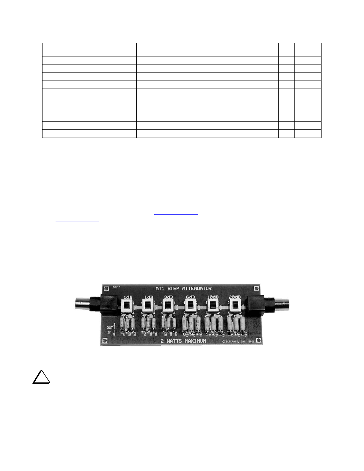
Assembly Procedure
The finished Attenuator is shown in Figure 1. We recommend you follow the assembly procedure below, and refer to this
figure as needed.
Figure 1. Assembled AT1 Step Attenuator.
i
Use adequate ventilation when soldering; avoid inhaling smoke or fumes. Always wash your hands after
handling solder, as lead residue is highly toxic.
When applying solder, use the minimum amount required to surround the component lead and make good contact with its
printed-circuit pad. You don't need a "fillet" (build-up) of solder. This will avoid unwanted solder bridges and any need to
clean the PC boards.
The solder must flow onto both the component lead and its PC board pad. To ensure that both will be heated at the same time,
the tip of the iron should contact both the component lead and the PC board pad before solder is applied.
2
Page 3

Solder joints should be clean and shiny. If a joint appears dull or has fine cracks, it is probably cold. Cold solder joints should
be cleaned and re-soldered. First, use solder wick (desoldering braid) to remove the old solder. Then apply fresh solder. If
you have many cold solder joints, it probably indicates that your soldering iron temperature is too low, or that the tip or
solder itself is defective.
i
The resistors must be placed slightly above the board as described below so that cooling air can flow easily if
you operate the attenuator near its upper power limit.
resistor on the board so it touches the spacer and spread the leads on the bottom to hold it in place (see Figure 2). Do not pull
the resistors tight against the wooden spacer. You’ll need to remove the spacer later. Working from left to right:
Place the wooden spacer across the board between the solder pads for resistors R1 through R9, then position each
__ R1, 910Ω (911)
__ R4, 910Ω (911)
__R7, 300Ω (301)
__ R2, 5.6Ω (5R6)
⇒
__R5, 5.6Ω (5R6)
⇒
__R8, 18Ω (180)
⇒
⇒
⇒
⇒
__ R3, 910Ω (911)
__R6, 910Ω (911)
__R9, 300Ω (301)
Figure 2. Spacing Resistors Above the Board.
Solder each resistor and clip its leads flush with the bottom of the board.
Following the same procedure, reposition the wooden spacer between the solder pads R10 thro ugh R18 and install those
resistors.
__R10, 150Ω
__R13, 100Ω
__R16, 62Ω
Remove the wooden spacer.
Position one of the slide switches in the outline next to the SW1 (1dB) marking on the board so the pins stick through
the solder pads. While holding the switch against the board, turn it over and touch one of the pins and solder pad with your
hot iron carrying a fresh drop of solder to tack-solder the switch in place.
Inspect the switch to ensure the pins on all four corners have their shoulders sitting flush against the board. If necessary
heat the tack-soldered pin while pressing down on the switch to position it against the board.
When you are satisfied with the switch position, solder the nine remaining pins, then go back and solder the first pin
properly.
In the same manner, install the remaining slide switches:
__R11, 39Ω (390)
⇒
__R14, 68Ω
⇒
__R17, 240Ω
⇒
⇒
⇒
⇒
__R12, 150Ω
__R15, 100Ω
__R18, 62Ω
__ SW2: 1 dB __ SW3: 3 dB __ SW4: 6 dB __ SW5: 10 dB __ SW6: 20 dB
3
Page 4

i
s
Normally the BNC jacks J1 and J2 will be installed on top of the board within the silk screened outline.
However, if you are planning to use the AT1 in an enclosure, you may optionally mount J1 and J2 on the bottom of
the board or use connectors that orient the jacks perpendicular to the board (see Assembly Options on page 2).
Install BNC jacks J1 and J2. Note that there are extra ground solder pads provided for those who wish to mount the
jacks differently for use in an enclosure. Trim the two longer pins flush after soldering.
__ J1
⇒
__ J2
If desired, install the rubber feet on the bottom of the board. Separate the feet, then remove the protective backing from
each foot and place one at each corner on the bottom of the board.
Checkout and Calibration
The AT1 Step Attenuator requires no calibration. Its accuracy is fixed by the value of
the resistors used. You can confirm that you have all the resistors in the correct
positions by checking the resistance of each attenuator section as described under
Troubleshooting on page 5.
Operation and Applications
If you’ve not owned a good step attenuator before, below are a few examples of how it
can be immediately useful in your station.
General Operation
RF is applied to one BNC connector and the attenuated signal is available at the other
BNC connector. The AT1 is a symmetrical design for use in a 50 ohm impedance line;
either connector may be used as the input or the output. With all the switches in the up
(OUT) position there is no significant attenuation. You can select any level of
attenuation from zero to 41 dB in 1 dB steps by throwing a combination of switches to
the IN position and adding the dB values of each switch. For example, you can obtain
15 dB of attenuation by placing the 10 dB, 3dB and both 1 dB switches to IN
(10+3+1+1=15 dB).
The attenuation in dB represents a ratio. It indicates how much the signal at the output
has been attenuated relative to the input. The value in dB may be expressed as a ratio in
power, voltage or current. You can calculate these ratios using the formulas in Figure 3
or you can refer to Table 1. Table 1 shows the ratios for all levels of attenuation from
1 dB to 41 dB in 1 dB steps for power (W), or for voltage or current (E/I). For example,
if you apply 1watt of power to the AT1 and select 15 dB of attenuation, the power at the
output would be 1 watt divided by 31.6 = 0.0031 watts or 3.1 milliwatts. Conversely, at
15 dB the level at the input to the AT1 is 31.6 times larger than the output. If you are
comparing current or voltages, use the ratios in the E/I column.
dB
A
A
dB = 10 LOG
dB = 20 LOG
or
B
A
or
B
Figure 3. Decibel Formulas.
QRPp Operation
The 2-watt power capability of the AT1 makes it ideal for QRPp experimentation.
Simply connect the AT1 between the output of your 2-watt or less transmitter and the antenna or antenna tuner. With all the
switches in the up (OUT) position, there is no attenuation. Now you can reduce power by throwing the switches to IN. For
= 10
B
A
= 10
B
10
where A and B are watts
dB
20
where A and B are volts or amp
Table 1.
Decibel Conversion.
dB
1 1.3 1.12
2 1.6 1.26
3 2.0 1.41
4 2.5 1.58
5 3.2 1.78
6 4.0 2.00
7 5.0 2.24
8 6.3 2.51
9 7.9 2.82
10 10.0 3.16
11 12.6 3.55
12 15.8 3.98
13 20.0 4.47
14 25.1 5.01
15 31.6 5.62
16 39.8 6.31
17 50.1 7.08
18 63.1 7.94
19 79.4 8.91
20 100 10.0
21 126 11.2
22 158 12.6
23 200 14.1
24 251 15.8
25 316 17.8
26 398 20.0
27 501 22.4
28 631 25.1
29 794 28.2
30 1000 31.6
31 1259 35.5
32 1585 39.8
33 1995 44.7
34 2512 50.1
35 3162 56.2
36 3981 63.1
37 5012 70.8
38 6310 79.4
39 7943 89.1
40 10000 100.0
41 12589 112.2
Ratio
W E/I
4
Page 5

example, if your transmitter is producing 1 watt and you select 6 dB of attenuation, the power you are feeding to the antenna
is 1 watt divided by 4.0 (from Table 1) = 0.25 watts or 250 milliwatts.
If you are using the attenuator with a transceiver that has a single antenna connection for both receive and transmit, the AT1
will attenuate the received signal as well unless you place all the switches to OUT when receiving.
S-Meter Evaluation
You can determine how sensitive the S-meter in any receiver is to change in signal levels with the AT1. This is best done
with a calibrated signal generator such as the Elecraft XG1 or XG2 but off-air signals can produce usable results as well.
Connect the AT1 between your receiver antenna input and your antenna or the signal generator output.
Tune in your signal generator or a steady on-air signal with a level of about S9 and note the S-meter reading. Now switch in
attenuation until the signal level drops exactly one S-unit and note the attenuation needed. Most S-meters are assumed to
represent about 6dB change per S-unit, but this can vary widely from one receiver to another. If, for example, your S-meter
does indicate a drop of one S-unit for each 6dB increase in the attenuation, you can see from Table 1 that a station who
changes its power from 5 watts to 20 watts (ratio of 4.0 from the table) should show exactly a one S-unit increase on your
meter.
Add attenuation to see if the same amount is required to reduce the signal additional S-units over the range of your receiver’s
S-meter. Making a note of this response will help you evaluate other station’s signals when they experiment with changes.
Receiver Weak Signal Performance
If you have a calibrated, low-level signal generator such as the Elecraft XG1 or XG2, you can use it with your AT1 to better
understand the weak signal capability of a receiver. Connect the AT1 between the signal generator and the receiver antenna
connector. Start with a signal level of 1 µV from the generator and set all of the attenuator switches to OUT. Tune in the
signal, then start adding attenuation on the AT1 until the signal drops to the threshold of your ability to hear it. For example,
you might find that you can just hear the signal with 22 dB of attenuation switched in. Looking up 22 dB in Table 1, the E/I
column (for volts and current since we’re working in m i cro vol t s) s hows a rat i o of 12.6. Dividing 1 µV by 12.6 yields 0.079
µV for the signal level at the receiver antenna connector. Note that you can hear weaker signals with a narrower receiver
bandwidth. That’s because there is less noise being passed through the receiver to compete with the signal.
Troubleshooting
The most likely causes of trouble with your AT1 will be:
1. You’ve installed a resistor incorrectly.
2. A resistor has been damaged, usually by overheating if more than 2 watts was applied to the AT1 for any length
of time. Overheating typically will cause a resistor to increase in value.
3. A solder bridge occurred between pads or a joint was missed, producing an intermittent or high-resistance
connection. A missed solder connection may not show up until some time after you built the unit, as oxidation
slowly accumulates on the surfaces.
Check all the solder connections on the bottom of the board with a strong magnif ier. Look especially closely at the 10 solder
pads for each switch. Make sure all of them are properly soldered and that there are no solder bridges.
You can test each attenuator position for the proper resistance as follows:
Connect a DMM set to measure ohms between the center pin and ground at one BNC connector. Make sure nothing is
connected to the other BNC.
Set all the switches to OUT, then switch each one, one at a time, to IN and compare the resistance shown on your DMM
with those below. The ranges shown below are what the tolerances of the resistor may allow. The actual possible error may
be greater than shown, depending upon the accuracy of your DMM.
1 dB: 456.4 ± 22.8 ohms 3 dB: 154.4 ± 7.7 ohms 6 dB: 83.6 ± 4.2 ohms
10 dB: 62.6 ± 3.1 ohms 20 dB: 51.4 ± 2.6 ohms
5
Page 6

Circuit Description
Refer to the schematic diagram below. There are six independent resistive attenuator networks. A pi-section circuit is used so
the circuit is symmetrical. Either connector may be used for the input or output. Each attenuator network may be switched in
or out of the signal path by the associated slide switch.
6
 Loading...