

Page 1

ELECRAFT AF1 Active Audio Filter
Assembly and Operating Manual
E740102: Revision B, February 8, 2012
Copyright © 2012 Elecraft; All Rights Reserved
Introduction
The Elecraft AF1 is a versatile audio filter that can be used with any receiver or transceiver. It can improve intelligibility of
CW, phone, or data signals, and is especially well suited to radios that have inadequate I.F. or audio filtering. The AF1 uses
straightforward analog circuitry and no surface-mount components, so it’s an ideal project for first-time kit builders.
A rotary switch on the unit allows you to select a low-pass characteristic with adjustable upper frequency roll-off, or a narrow
bandpass characteristic. The bandpass filter offers two levels of selectivity, and its center frequency may be tuned from about
350 Hz to about 950 Hz. The low-pass filter is active during bandpass operation, allowing you to further control the upper
frequency response. The output amplifier drives low impedance phones or a small loudspeaker. Power can be supplied via
either an on-board 9-V battery or an external supply. An LED indicates power on/off status.
Specifications
Size: 5-1/2” L x 2-7/8” W x 7/8” H (14 cm x 7.3 cm x 2.2 cm). Height not including feet or knobs.
Internal Power: 9V battery.
External Power: 7-14 V (8 V min. recommended).
Current Drain: 10 mA minimum volume to 100 mA full volume, typical.
Functions: Low pass plus two levels of bandpass with tunable center frequency in bandpass mode.
See Typical Response Plots on page 9.
Tools Required
You will need the following tools to build this kit:
Fine-tip temperature-controlled ESD-safe soldering station with 700 to 800F tip (370-430C). Recommend a spade
tip no greater than 0.05” (1.3 mm) wide.
IC-grade solder (Kester #44 or equivalent). Small diameter solder (e.g. .031”) is easiest to work with on small
printed circuit boards. DO NOT use acid-core solder, water-soluble flux solder, additional flux or solvents.
Small, #2 Phillips screwdriver.
Needle-nose pliers.
Diagonal cutters.
Small wrench or driver for 4-40 nut.
Digital Multimeter (DMM) with voltage, resistance and diode-checking functions is useful for confirming the value
of components. A DMM with capacitance measurement capability is desirable, but not required.
Desoldering tools and supplies are invaluable. Narrow solder wick or a good vacuum desoldering tool such as the
Soldapullt® model DS017LS are recommended.
Refer to www.elecraft.com for tool sources and solder recommendations.
Parts List
We strongly recommend that you do a complete inventory before beginning assembly. The inventory helps you correctly
identify all the parts to avoid mistakes during assembly.
Identifying Parts
In some cases the component marking is self-evident. A 1N4007 diode, for example, will have “1N4007” stamped on its
body. When the markings are not so obvious, the marks you should find to identify individual components are shown in
parenthesis in the parts list and text. These may be numbers such as “(103)” on capacitors or colors on resistors such as
Elecraft • www.elecraft.com • 831-662-8345
Page 2

“(brn-blk-red)”. Look for the color band sequence starting near one end of the component. Some resistors have dark blue
bodies that make identifying the colors difficult. Use your DMM to verify the value if you aren’t sure. Remember that your
DMM usually will indicate a value close to, but not exactly what is shown, due to normal tolerances in the components and
the DMM.
There may be more numbers, letters or color bands on a component than those shown in parenthesis. The additional markings
may change from unit to unit and are not important for identifying the part supplied with the kit.
Reference. Designator Description Qty
Misc. AF1 Audio Filter Printed Circuit Board 1 E100310
B1 Battery Holder 1 E980074
C1, C10 1µF 50V Electrolytic Capacitor 2 E530022
C2, C3, C11 470µF 25V Electrolytic Capacitor 3 E530084
C4, C7, C8 , C9, C13 .01µF (103) Capacitor 5 E530009
C5 .0022µF (222) Capacitor 1 E530054
C6 .1µF (104) Capacitor 1 E530011
C12 .047µF (473) Capacitor 1 E530025
R1 1.5k (brn-grn-blk-brn-brn) 1/4W Resistor 1 E500034
R2, R4, R7, R14 1.0k (brn-blk-red) 1/4W Resistor 4 E500013
R3 15k (brn-grn-org) 1/4W Resistor 1 E500060
R6 10k (brn-blk-org) 1/4W Resistor 1 E500015
R8, R11 180k (brn-gry-yel) 1/4W Resistor 2 E500068
R9, R12 680Ω ((blu-gry-brn) 1/4W Resistor 2 E500040
R17, R13 360k (org-blu-yel) 1/4W Resistor 2 E500264
R16 10Ω (brn-blk-blk) 1/4W Resistor 1 E500054
R18 22k (red-red-org) 1/4W Resistor 1 E500090
R10 5k dual potentiometer, linear taper, 6 pin 1 E520019
R15 10K (10KD) potentiometer 1 E520018
R5 50K (50KB) potentiometer 1 E520017
D1, D2 1N4007 Diode 2 E560001
D3 LED, Red, Ultra bright 1 E570025
J1, J3 Jack, Stereo, 3.5 mm 2 E620027
J2 Jack, 2.1 mm, 12VDC power 1 E620026
SW1 Switch, Rotary, 3 Pole, 4 Position, Non-Shorting, PC 1 E640033
U1 LM348 Integrated Circuit 1 E850231
U2 LM386 Integrated Circuit 1 E600022
Hardware Screw, Pan Head, Black Machine, 4-40 4 E700008
Hardware Lock Washer, Internal Tooth, #4 4 E700010
Hardware Nut, #4-40 4 E700011
Misc Knob w/set screw for 1/4 inch shaft 4 E700118
Misc Rubber Foot 4 E700024
Misc #24 Wire, Solid, Green, Insulated 6” E760008
Part
Number
Assembly Options
The AF1 is designed to operate as a stand-alone unit without an enclosure. In the event you want to build it into existing
equipment or its own enclosure:
1. Four holes are provided in the board that you may use with your own #4 hardware and spacers as needed to mount
the unit instead of using the rubber feet.
2. The battery may be mounted on the top (component side) or bottom of the board or you may choose not to install the
battery holder if you are going to power your AF1 only from an external source.
2
Page 3
Assembly Procedure
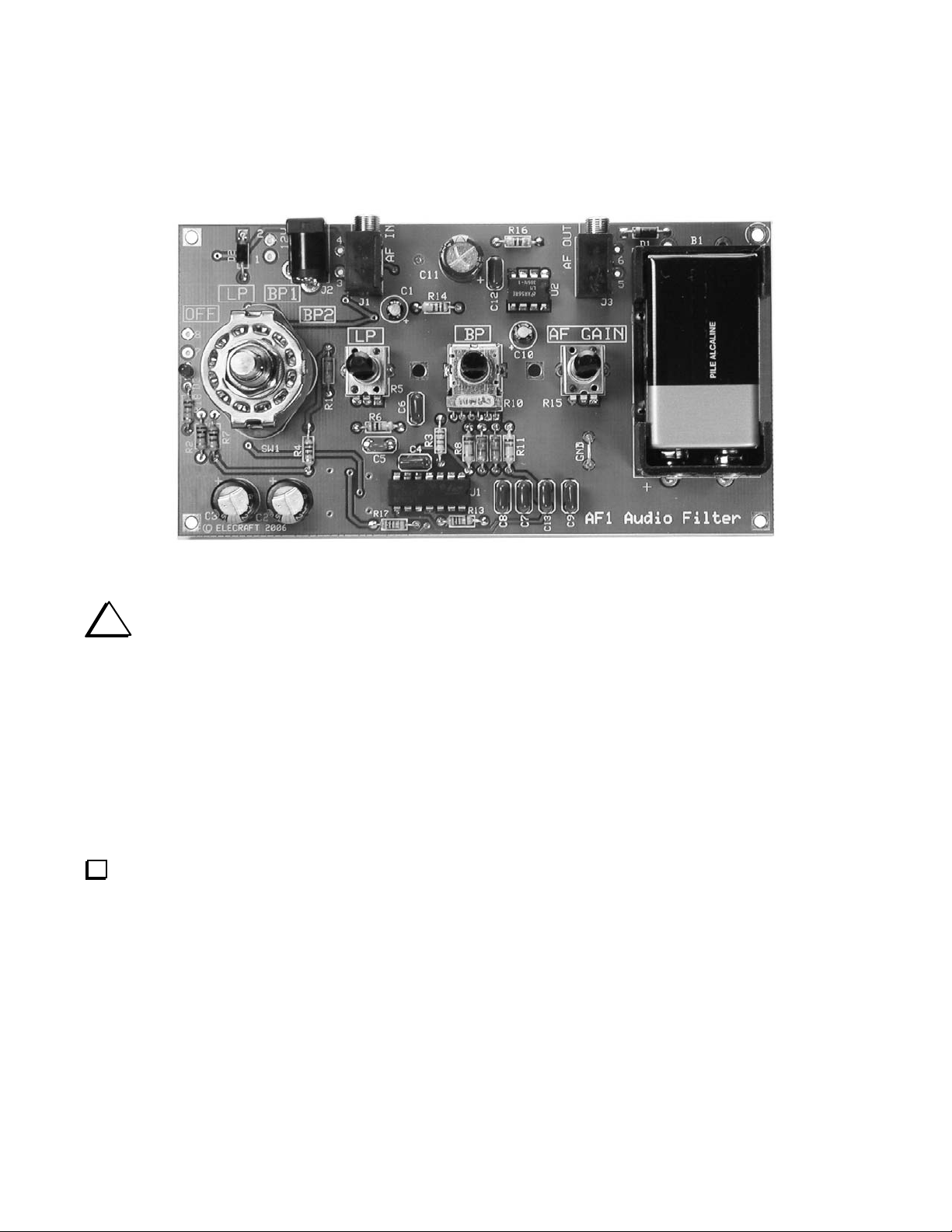
The finished audio filter is shown in Figure 1. The knobs were left off to better show the components on the board. We
recommend you follow the assembly procedure below, and refer to this figure as needed.
Figure 1. Assembled Audio Filter.
i
Use adequate ventilation when soldering; avoid inhaling smoke or fumes. Always wash your hands after
handling solder, as lead residue is highly toxic.
When applying solder, use the minimum amount required to surround the component lead and make good contact with its
printed-circuit pad. You don't need a "fillet" (build-up) of solder. This will avoid unwanted solder bridges and any need to
clean the PC boards.
The solder must flow onto both the component lead and its PC board pad. To ensure that both will be heated at the same time,
the tip of the iron should contact both the component lead and the PC board pad before solder is applied.
Solder joints should be clean and shiny. If a joint appears dull or has fine cracks, it is probably cold. Cold solder joints should
be cleaned and re-soldered. First, use solder wick (desoldering braid) to remove the old solder. Then apply fresh solder. If
you have many cold solder joints, it probably indicates that your soldering iron temperature is too low, or that the tip or
solder itself is defective.
flush on the bottom. If you position the board so the legends are right side up, you can work from left to right across the
board following the order given below. Save one of the clipped leads. You will use it to make a ground test point later.
Install the fixed resistors listed below. Position each resistor within the outline on the PC board, solder and trim the leads
__ R18, 22k (red-red-org)
__ R7, 1K (brn-blk-red)
__ R1, 1.5k (brn-grn-blk-brn)
__ R17, 360k (org-blu-yel)
__ R3, 15k (brn-grn-org)
__ R8, 180k (brn-gry-yel)
__ R12, 680Ω ((blu-gry-brn)
__ R16, 10Ω (brn-blk-blk)
__ R2, 1K (brn-blk-red)
__ R4, 1K (brn-blk-red)
__ R6, 10k (brn-blk-org)
__ R14, 1.0k (brn-blk-red)
__ R13, 360k (org-blu-yel)
__ R9, 680Ω ((blu-gry-brn)
__ R11, 180k (brn-gry-yel)
3
Page 4

Install the capacitors listed below just as you did with the resistors in the previous step:
FLARED
__ C5, .0022µF (222)
__ C6, .1µF (104)
__ C8, .01µF (103)
__ C13, .01µF (103)
__ C4, .01µF (103)
__ C12, .047µF (473) See note.
__ C7, .01µF (103)
__ C9, .01µF (103)
Note: The + symbol next to outline for C12 refers to electrolytic capacitor C11
that you’ll install later. C12 may be installed oriented either way, just like the
other capacitors in this group.
Locate LED D3. Note that one lead is slightly longer than the other. Insert the long lead in the lower, round solder pad
in the space for D3 on the left edge of the board. Position the LED as close to the board as it will fit. Solder and trim the leads
flush with the bottom of the board.
Locate diodes D1 and D2 (1N4007). Note the silver band at one end of the diode body. Install the diodes with the silver
stripe aligned with the stripe on the silk screened outline on the board.
__ D2, 1N4007 (near upper left corner)
__ D1, 1N4007 (near upper right corner)
Inspect the leads of one of the electrolytic capacitors. Note that there is a stripe with a – on the body to identify the
negative lead. The negative lead must be inserted in the round solder pad on the board. The positive lead must be inserted
in the square solder pad. There is a + symbol near that pad. The positive lead is slightly longer on most capacitors. Install the
electrolytic capacitors as follows:
__ C2, 470µF
__ C11, 470µF
__ C3, 470µF
__ C10, 1µF
__ C1, 1µF
Bend the clipped resistor lead you saved earlier into a “U” that fits into the solder pads at each end of the GND test point
near C9. Solder the lead into the pads with the loop high enough above the board to easily clip a test probe lead onto it.
Install U1 (LM348) as follows:
Place U1 on the board where shown by the outline near the bottom center. If the pins are spread too wide to fit, place
U1 on its side on a solid, flat surface and rock it gently to bend all the pins inward slightly as shown in Figure 2. Do
the same on both sides until it fits into the solder pads on the board.
Align the end of U1 that has a notch or dimple molded in the case
with the notch on the silk screened outline.
Hold U1 in place, wet the tip of your soldering iron with solder and
touch one of the corner pins on the bottom of the board to tack-solder
it in place.
PRESS AND
ROCK TO
STRAIGHTEN
STRAIGHT
Make sure U1 is correctly positioned and flat against the board, then
solder the remaining pins.
Figure 2. Straightening I.C. Pins.
Reheat the tack-soldered pin as needed to ensure it is properly
soldered.
Install U2 (LM386) using the same procedure you used for U1.
Install the 12VDC power connector, J2, as follows:
Position the connector over the J2 outline on the board.
Tack-solder one pin to hold it in place.
Check the position of the connector. If necessary reheat the soldered pin to adjust it.
Solder the remaining two terminals, then finish soldering the terminal you tacked in place.
4
Page 5

Install the stereo jacks using the same procedure you used for the 12VDC connector above:
J
R
__ J1
If the circuit board in your kit is Revision A (shown in the lower left corner on the top of the board), make the following
changes so it will work properly with a monaural plug at the input and a stereo plug at the output. Skip this step if your circuit
board is a later revision.
At the pins of J1 (AF IN) on the bottom of the board, use a sharp knife to cut and remove the segment of the trace
shown below. Use the green insulated wire to make a jumper to reach between the pin on J1 shown and the small
hole at the circuit via where the trace passes through to the top of the board. This change isolates the ring connection
so a monaural plug at J1 it won’t short the audio to ground.
At the pins of J3 (AF OUT) on the bottom of the board, install a jumper between the pins shown below. Use a short
section of the green insulated wire or a discarded component lead. Take care to ensure the middle connection of J3 is
not shorted to ground. This ties tip and ring together so audio is present on both at the output.
CIRCUIT
__ J3
CUT TRACE HERE
VIA
JUMPE
JUMPER
BE CAREFUL
NOT TO CREATE
A SHORT TO
GROUND HERE
J1 - AF IN
Figure 3. Rev. A Board Modifications.
Install 6-pin dual potentiometer R10 as follows:
Position R10 on the board. Be sure all six pins pass through their respective solder pads, then press down on the
body of the potentiometer, if necessary, to snap it in place. Do not push on the shaft.
Solder only one pin, then inspect the potentiometer to be sure it is sitting flat against the board. Look at it from two
directions to be sure the shaft is perpendicular to the board. If necessary, reheat the soldered pin and reposition the
R10.
Solder all six signal pins and the two side clips to the board.
Install potentiometers R5 and R15 using the same procedure you used for R10:
__ R5 (50KB)
Install rotary switch SW1 as follows:
Position SW1 inside its outline on the board. Note that the pins will fit through the solder pads when the switch is
oriented one way.
Solder one pin and inspect the switch to be sure it is perpendicular to the board, just as you did for the
potentiometers.
Solder all the pins.
__ R15 (10KD)
2 - AF OUT
5
Page 6

i
The battery holder many be installed on the top or the bottom of the board. No rmally you will want to install
it on the top so the finished unit will sit flat on its feet. However, if you plan to install the filter in an enclosure, you can
mount the battery holder on the bottom of the board. Solder pads are provided to mount the holder on either side as
indicated on the circuit board. Also, if plan to supply only external power to the filter, you can leave the battery
holder off entirely.
Install the battery holder as follows:
Position the battery holder on the board within the outline. Be sure you have it on the correct side of the board.
Unless you have a special need, you will want to put it on the top side along with the other components. Do not
solder yet.
Attach the holder to the board with the 4-40 screws in four places, using lock washers and nuts. The screw heads
should be on the holder side so the battery will fit correctly. You may need to bend the battery holder terminals
slightly to align the screw holes with those in the board.
Solder the two terminals to the pads and trim them flush.
Attach the four feet to the corners of the board on the bottom. If you plan to build the filter into a rig or separate
enclosure, you may leave the feet off and use the four corner holes for mounting the filter.
Attach the four knobs to the rotary switch and potentiometer shafts. Line up the index mark on the knob for the rotary
switch so it is pointing to OFF when the switch is rotated to the fully left position. The potentiometer shafts may wobble a
little because long shafts are required to approximate the height of the rotary switch shaft.
Checkout and Operation
If you have difficulty with the following steps, refer to the circuit description and troubleshooting notes in the following
sections.
Install a 9-volt battery in the holder or connect a d-c supply between 9 and 14VDC to J2 (positive to center pin).
Connect an audio source to the AF IN jack (J1). This can be a headphone output from your receiver or other audio
source.
Connect your headphones or a small loudspeaker to the AF OUT jack (J3).
Position the LPF, BP and AF GAIN pots to minimum (counter-clockwise).
Turn SW1 to LP (low-pass) position. The red LED D3 should light.
Rotate the AF GAIN clockwise for a convenient audio level in the phones or loudspeaker.
Rotate the LP pot clockwise. You’ll hear high frequency sound increase in volume as you turn the pot. This is raising
the cutoff frequency from minimum (fully counter-clockwise) to maximum. Leave LP fully clockwise.
Rotate SW1 to BP1 (bandpass filter 1) position. If possible supply a single frequency tone to the input (such as tuning in
a CW signal on your rig).
Rotate the BP pot. The volume of the signal will rise abruptly as you pass its frequency.
Rotate SW1 to BP2 (bandpass filter 2) position and repeat tuning the BP pot. You should notice that the adjustment is
now noticeably sharper. BP 2 adds a second bandpass filter to further improve the selectivity.
i
Be sure the LPF is always set so it will pass the frequency you’ve chosen for the bandpass filter. You can set
the LPF cutoff frequency close to the BPF frequency so it aids in rejecting high-frequencies above the bandpass
frequency.
6
Page 7

Circuit Description
Refer to the schematic diagram on page 8. The filter circuit uses a quad operational amplifier integrated circuit that features
excellent isolation between the stages. Audio applied at J1 passes through a low-pass filter formed U1A and B. Potentiometer
R5 varies the high-frequency cutoff. U1C and D form two independent bandpass filters whose center frequencies are
controlled by ganged potentiometers R10A and R10B. These stages tune together so they are both centered on the same
frequency at all times. U2 is an audio amplifier that drives the AF output.
Rotary Switch SW1 has three sections. Section B selects the output of the low-pass filter, the output of the low-pass filter
plus one bandpass filter, or the output of the low-pass filter plus both bandpass filters. In the OFF position, SW1C routes the
audio from the input directly to the output so you don’t have to remove the filter when it is not in use. SW1A controls power
to the filter.
The power circuit allows you to use either a 9V battery or an external power supply. Diodes D1 and D2 isolate the battery
from an external supply to avoid the possibility of an external supply driving current into the battery and causing it to rupture.
Troubleshooting
If LED D3 does not light when SW1 is positioned to LP, check the orientation of diode D1 (if using internal battery) or D2 if
using an external supply. Test points 2 (+) and 1 (-) also allow you to check to be sure voltage is present at J2. Next check the
voltage across test points 7(+) and 8(-). If the voltage is above about 2VDC, D3 is either installed backwards or it is
defective.
If there is power but no audio output except when SW1 is in OFF position, turn the AF GAIN pot fully clockwise and touch a
metal test probe to the center pin of pot R15. You should hear a slight click, indicating that amplifier U2 is working. If so, the
problem is most likely in the circuits of U1A or U1B. Similarly, loss of output or function in BP1 indicates a problem in the
U1C circuit and problems in BP2 indicates a problem with the U1D circuit (see the schematic diagram on the next page). The
usual cause of problems in these stages is an incorrectly installed part, an electrolytic capacitor installed backwards or a
solder bridge across two adjacent pads. Use a magnifier and carefully inspect the board for correct component values and
solder bridges around the affected circuit.
7
Page 8
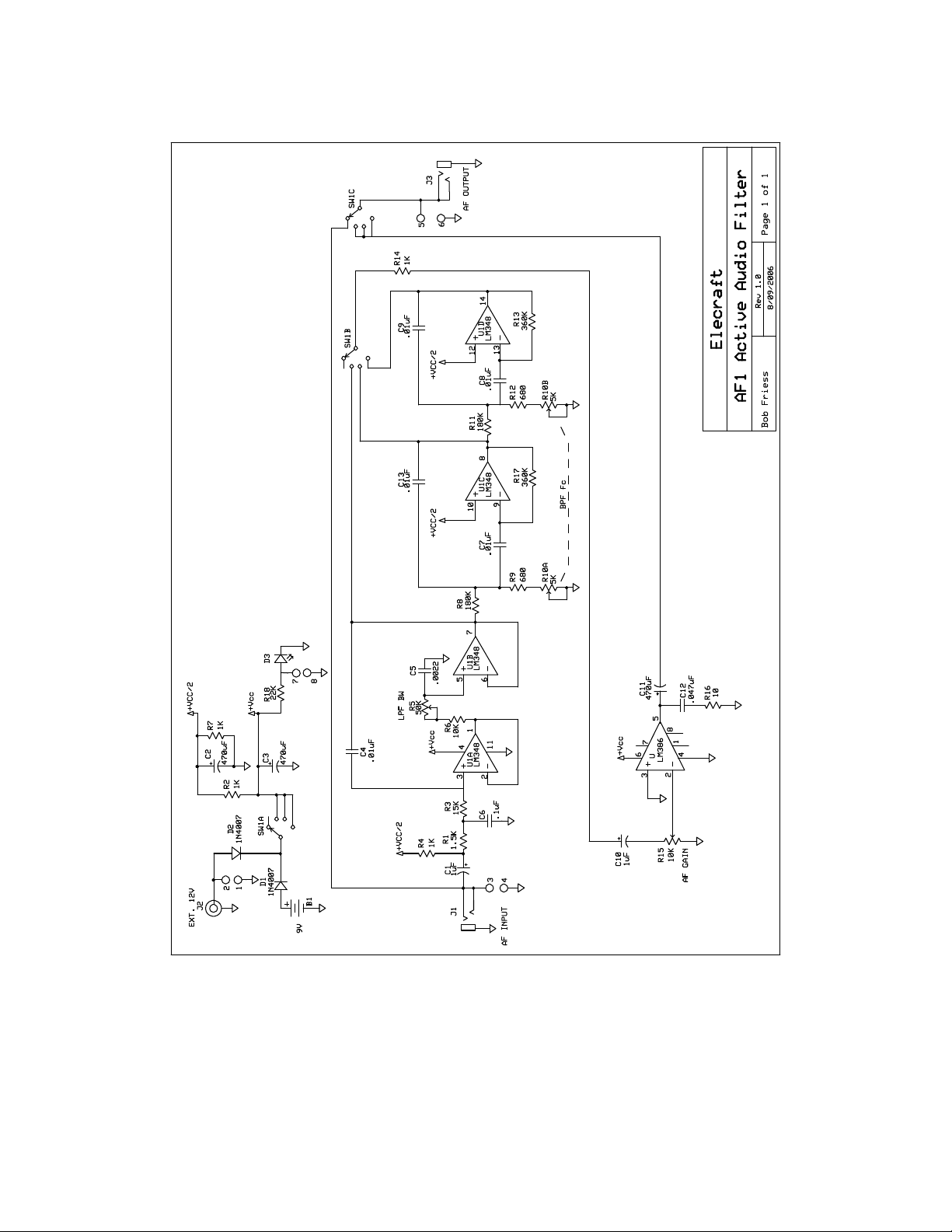
Schematic Diagram
8
Page 9

Typical Response Plots
/
/
O
The following plots AF1 plots were made with a network analyzer. The results should be typical of your filter.
L
W PASS FILTER AT MAXIMUM BANDWIDTH
LOW PASS FILTER AT MINIMUM BANDWIDTH
5 dB/Division
0.3 5.04.063.122.18
BANDPASS FILTER POSITION 1 BANDPASS FILTER POSITION 2
LOW PASS FILTER SET TO MAXIMUM BANDWIDTH LOW PASS FILTER SET TO MAXIMUM BANDWIDTH
0.1 0.3 0.5 0.7 0.9 1.0
1.24
kHz
Center
Frequency
600 Hz
kHz
BANDPASS FILTER POSITION 2
LOW PASS FILTER SET TO MINIMUM BANDWIDTH
5.04.063.122.18
5dB
Division
0.3
0.1
1.24
kHz
Center
Frequency
600 Hz
0.3 0.5 0.7 0.9 1.0
kHz
5dB
Division
Center
Frequency
600 Hz
0.1 0.3 0.5 0.7 0.9 1.0
kHz
9
 Loading...