DYNEX MAS7001NL, MAS7001NE, MAS7001ND, MAS7001NC, MAS7001FS Datasheet
...
MA7001
1/15
The MA7001 512 x 9 FIFO is manufactured using Dynex
Semiconductor's CMOS-SOS high performance, radiation
hard, 3µm technology.
The Dynex Semiconductor Silicon-on-Sapphire process
provides significant advantages over bulk silicon substrate
technologies In addition to very good total dose hardness and
neutron hardness >1015n/cm2, the Dynex Semiconductor
technology provides very high transient gamma and single
event upset performance without compromising speed of
operation The Sapphire substrate also eliminates latch-up
giving greater flexibility of use in electrically severe
environments.
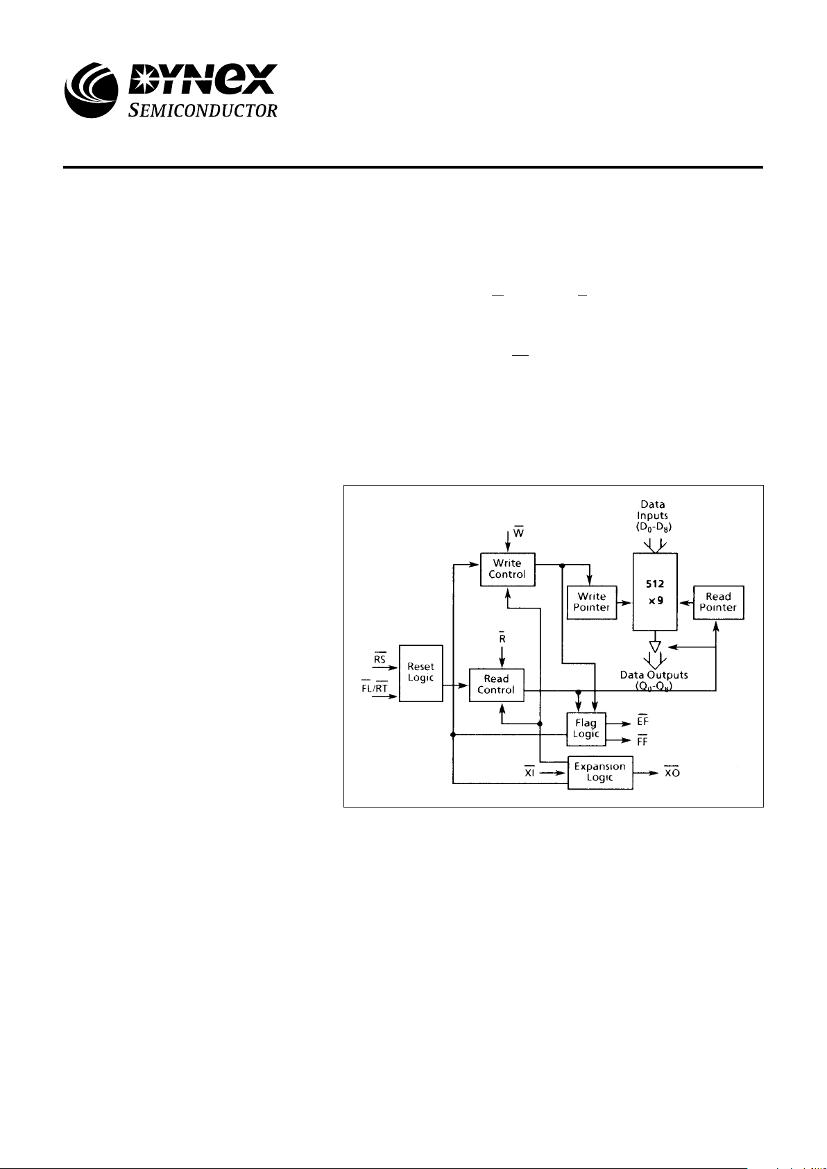
The MA7001 implements a First-ln First-Out algorithm that
reads and writes data on a first-in first-out basis. The dual-port
static RAM memory is organised as 512 words of 9 bits (8 bit
data and 1 bit for parity or control purposes).
Sequential read and write accesses are achieved using a
ring pointer architecture that requires no external addressing
information. Data is toggled in and out of the device by using
the WRITE (W) and READ (R) pins.
Full and Empty status flags prevent data overflow and
underflow. Expansion logic on the device allows for unlimited
expansion capability in both word size and depth. A
RETRANSMIT (
RT) feature allows for reset of the read pointer
to its initial position to allow retransmission of data.
The device is designed for applications requiring
asynchronous and simultaneous read/write in multiprocessing
and rate buffering (sourcing and sinking data at different rates
eg. interfacing fast processors and slow peripherals).
FEATURES
■ Radiation Hard CMOS-SOS Technology
■ Fast Access Time 60ns Typical
■ Single 5V Supply
■ Inputs Fully TTL and CMOS Compatible
■ -55°C to +125°C Operation
Figure 1: Block Diagram
MA7001
Radiation Hard 512x9 Bit FIFO
Replaces June 1999 version, DS3519-4.0 DS3519-5.0 January 2000

MA7001
2/15
DC CHARACTERISTICS AND RATINGS
Symbol Parameter Min. Max. Units
V
DD
Supply Voltage -0.5 7.0 V
V
IN
Input Voltage -0.3 VDD+0.3 V
T
A
Operating Temperature -55 125 °C
T
S
Storage Temperature -65 150 °C
Stresses above those listed may cause permanent
damage to the device. This is a stress rating only and
functional operation of the device at these conditions, or at
any other condition above those indicated in the
operations section of this specification, is not Implied
Exposure to absolute maximum rating conditions for
extended periods may affect device reliability.
Figure 2: Absolute Maximum Ratings
The following D.C. and A.C. electrical characteristics apply to pre-radiation at TA = -55°C to +125°C, VDD = 5V ±10% and post
100kRad(Si) total dose radiation at TA = 25°C, VDD = 5V ±10%. GROUP A SUBGROUP 1, 2, 3.
Symbol Parameter Conditions Min. Typ. Max. Unit
V
IH
Input logic '1' voltage - 2.0 - - V
V
IL
Input logic '0' voltage - - - 0.8 V
I
IL
Input leakage current (any input) (Note 4) Note 1 -10 - 10 µA
I
OL
Output leakage current (Note 4) Note 2 -50 - 50 µA
V
OH
Output logic '1' voltage l
OUT
= -1mA 2.4 - - V
V
OL
Output loglc '0' voltage l
OUT
= 2mA - - 0.4 V
I
DD1
Average VDD power supply current (Note 3) Freq = 10MHz - 70 100 mA
I
DD2
Average standby current (Note 3) R = W = RS = FL/RT = VDD/2 - 8 15 mA
I
DD3(L)
Powerdown current (Note 3) All Inputs = VDD -0.2V - - 3.0 mA
NOTES:
1. Measurements with VSS ≤ VIN ≤ V
DD
2. R > VIH, VSS ≤ V
OUT
≤ V
DD
3. IDD measurements are made wlth outputs open, VDD = 5.5V
4. Guaranteed but not measured at -55°C
Figure 3a: DC Electrical Characteristics

MA7001
3/15
AC CHARACTERISTICS
Characteristics apply to pre-radiation at TA = -55°C to +125°C, VDD = 5V ±10% and post
100kRad(Si) total dose radiation at TA = 25°C, VDD = 5V ±10%. GROUP A SUBGROUP 9, 10, 11.
Symbol Parameter Min. Max. Units
t
RC
Read Cycle Time 110 - ns
t
A
Access Time - 100 ns
t
RR
Read Recovery Time 25 - ns
t
RPW
Read Pulse Width (Note 2) 85 - ns
t
RLZ
Read Pulse Low to Data Bus at Low Z (Note 3) 10 - ns
t
DV
Data Valid from Read Pulse High 20 - ns
t
RHZ
Read Pulse High to Data Bus at High Z (Note 3) - 30 ns
t
WC
Write Cycle Time 100 - ns
t
WPW
Write Pulse Width (Note 2) 80 - ns
t
WR
Write Recovery Time 20 - ns
t
DS
Data Setup Time 40 - ns
t
DH
Data Hold Time 10 - ns
t
RSC
Reset Cycle Time (Note 3) 100 - ns
t
RS
Reset Pulse Width (Note 2) 80 - ns
t
RSR
Reset Recovery Time (Note 3) 20 - ns
t
RTC
Retransmit Cycle Time (Note 3) 100 - ns
t
RT
Retransmit Pulse Width (Note 2) 80 - ns
t
RTR
Retransmit Recovery Time (Note 3) 20 - ns
t
EFL
Reset to Empty Flag Low - 100 ns
t
REF
Read Low to Empty Flag Low - 90 ns
t
RFF
Read High to Full Flag High - 70 ns
t
WEF
Write High to Empty Flag High - 70 ns
t
WFF
Write Low to Full Flag Low - 90 ns
t
EFR
EF High to Valid Read (Note 3) 10 - ns
t
RPI
Read Protect Indeterminant (Note 3) - 35 ns
t
FFW
FF High to Valid Wrlte (Note 3) 10 - ns
t
WPI
Write Protect Indeterminant (Note 3) - 35 ns
Notes:
1. Timings referenced as in A.C. Test Conditions, figure 5
2. Pulse wldths less than minimum values are not allowed
3. Values guaranteed by deslgn, not currently tested
Figure 3b: AC Characteristics

MA7001
4/15
Symbol Parameter Conditions
FT Functionality VDD = 3-6V, FREQ = 100kHz - 9MHz
VIL = VSS, VIH = VDD, VOL ≤ 1.5V, VOH ≥ 1.5V
TEMP = -55 to +125°C, RADIATION 1MRAD TOTAL DOSE
GROUP A SUBGROUPS 7, 8A, 8B
Figure 3b: Functionality
Subgroup Definition
1 Static characteristics specified in Table 3a at +25°C
2 Static characteristics specified in Table 3a at +125°C
3 Static characteristics specified in Table 3a at -55°C
7 Functional characteristics specified in Table 3c at +25°C
8A Functional characteristics specified in Table 3c at +125°C
8B Functional characteristics specified in Table 3c at -55°C
9 Switching characteristics specified in Table 3b at +25°C
10 Switching characteristics specified in Table 3b at +125°C
11 Switching characteristics specified in Table 3b at -55°C
Figure 4: Definition of Subgroups

MA7001
5/15
Input Pulse Levels GND to 3.0V
Input Rise and Fall Times 5ns
Input Timing Reference Levels 1.5V
Output Reference Levels 1.5V
Output Load See Figure 7
Figure 5: AC Test Conditions
Symbol Parameter Conditions Max. Unit
C
IN
Input Capacltance (Note 1) VIN = 0V 7 pF
C
OUT
Output Capacitance (Notes 1 and 2) V
OUT
= 0V 12 pF
NOTES:
1. Characterized values, not currently tested.
2. With output deselected.
Figure 6: Capacitance
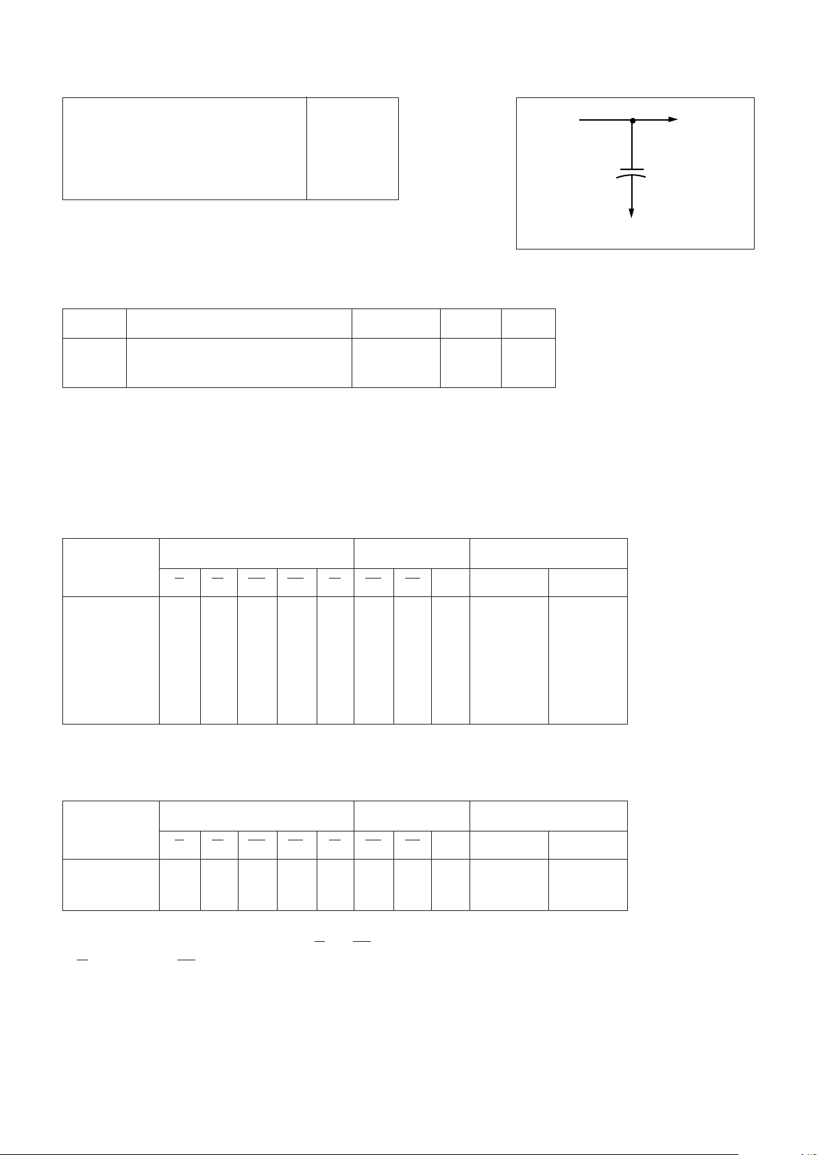
TRUTH TABLES
Input Output Pointer
Operation
R W RS RT Xl EF FF Data Read Write
Reset 1 1 0 x 0 0 1 Z Zero Zero
Retransmit* 1110011Z Zero N/C
Read 1→0x11011valid Increment N/C
Read x x 11001Z N/C N/C
Write x 1→0 1 1 0 x 1 x N/C Increment
Write x x 11010x N/C N/C
* Only available if less than 512 writes since last reset.
Figure 8: Single Device or Width Expansion: Read, Write, Reset and Retransmit
Input Output Pointer
Operation
R W RS FL Xl EF FF Data Read Write
Reset First 1100101Z Zero Zero
Reset Rest 1101101Z Zero Zero
NOTES:
1. See Modes of Operation for connections of
Xl and XO in depth expansion mode.
2. XI is connected to XO of previous device (Figure 12).
Figure 9: Depth Expansion: Reset and First Load
Output
under test
Test Point
LOAD 1
≤50pF*
Figure 7: Output Load
* Includes jig
and scope
capacitances
 Loading...