DYNEX GDU91-20221 Datasheet

GDU 91 20221
GDU 91-20221
Gate Drive Unit
Replaces March 1998 version, DS4569-3.1 DS4569-4.0 January 2000
This datasheet should be used in conjunction with the application note AN4571, GDU9X-XXXXX Series, Gate Drive Unit.
APPLICATIONS
■ Used with Gate Turn-Off Thyristors in high current switching
applications
I
FGM
I
G(ON)
dIGQ/dt 30A/µs
CONDITIONS - (UNLESS STATED OTHERWISE)
V1 = +5V V2 = +15V V3 = -15V
Test circuit GTO
GDU connection to GTO
Test circuit emitter and gate drive emitter
Test circuit emitter current
DG408BP
500mm CO - AX cable type RC5327230
Hewlett Packard versatile link HFBR1524
30mA
Test circuit receiver and gate drive receiver Hewlett Packard versatile link HFBR2524
ELECTRICAL CHARACTERISTICS
Parameter
KEY PARAMETERS
30A
4A
UnitsMax.Typ.Min.ConditionsSymbol
dI
dI
V
V
V
I
I
I
V1
I
V2
V3
1(Min)
2(Min)
3(Min)
FGM
G(ON)
FG
GQ
+5V PSU current
+15V PSU current
-15V PSU currentI
+5V PSU minimum
+15V PSU minimum
-15V PSU minimum
Peak forward gate current
On-state gate current
/dt
Rate of rise of positive gate current
/dt
Rate of rise of negative gate current
500Hz, 50% duty cycle
500Hz
500Hz, I
GTO Tj = 125˚C
= 1000A
T
-
-
-
-
-
Measured 10 - 75% I
IT = 1000A, 90% I
G(ON)
FGM
- 50% I
GQM
-
-
-
3.8
14.0
14.0
30
--
-30-
-
30
2.2 A
-
0.55 A
-
3.0 A
-
--
--
--
--
4
-
V
V
V
A
A
A/µs
A/µs
1/4

GDU 91 20221
TIMING CHARACTERISTICS
Parameter
No response pulse width of
†
t
t3*
t8*
t
t
1
t
t5*
t
*
t
2
4
input signal
Delay time emitter
current to receiver o/p
Turn-on delay emitter
†
current to 10% I
I
pulse width
FGM
FGM
Minimum on time
10% I
t
6
t
7
Receiver storage time
Turn-off delay.
Emitter current to 90% I
to 90% I
FGM
G(ON)
G(ON)
Minimum off time
90% I
G(ON)
to 10% I
FGM
Delay time
9
Gate volts to o/p emitter current
Turn-off delay
10
Gate volts to test receiver o/p
Storage time
11
Gate volts to o/p emitter current
Adjustable by R81 + R82
-
-
-
Adjustable by R37
-
-
Adjustable by R38 80
-
-
Measured at low I
GQM
23µs
0.2
5.0
-
80
0.8
1.5
-
-
-
25
-
-
-
-
0.2
-
0.8
-
1
0.1
-
UnitsMax.Typ.Min.ConditionsSymbol
0.4 µs
5.8 µs
-
µs
110 µs
1.2 µs
2.3 µs
110 µs
-
-
-
µs
µs
µs
t
12
Turn-on delay
Gate volts to test receiver o/p
Measured at low I
* t1,t3,t5,t8 are factory settings. † Adjustment of t1 alters t3. 1. Varies with I
t
FGM
I
1
dIFG/dt
0V
t
2
10µs
10%
t
3
Min. ON time
-8V
t
6
t
4
t
5
dI
/dt
GQ
t
9
t
10
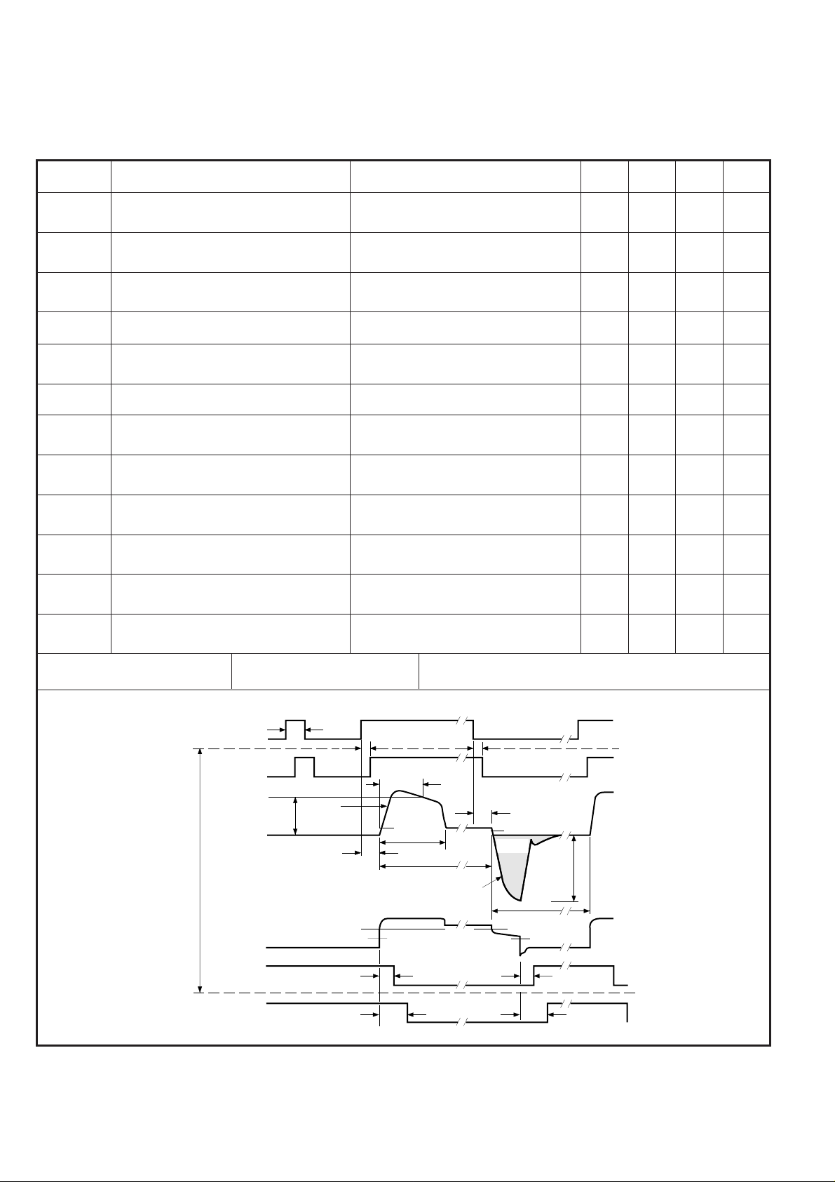
Test circuit
emitter current
Control card
receiver output
Gate current
Gate voltage
Gate Drive Unit Waveforms
Control card emitter current
Test circuit receiver output
GQM
I
-
GQM
due to gate lead impedance.
GQM
t
7
90% I
G(ON)
Q
GQT
t
8
Min. OFF
-8V
t
11
t
12
0.3
1
-
µs
2/4
 Loading...