

Page 1
SERVICE MANUAL
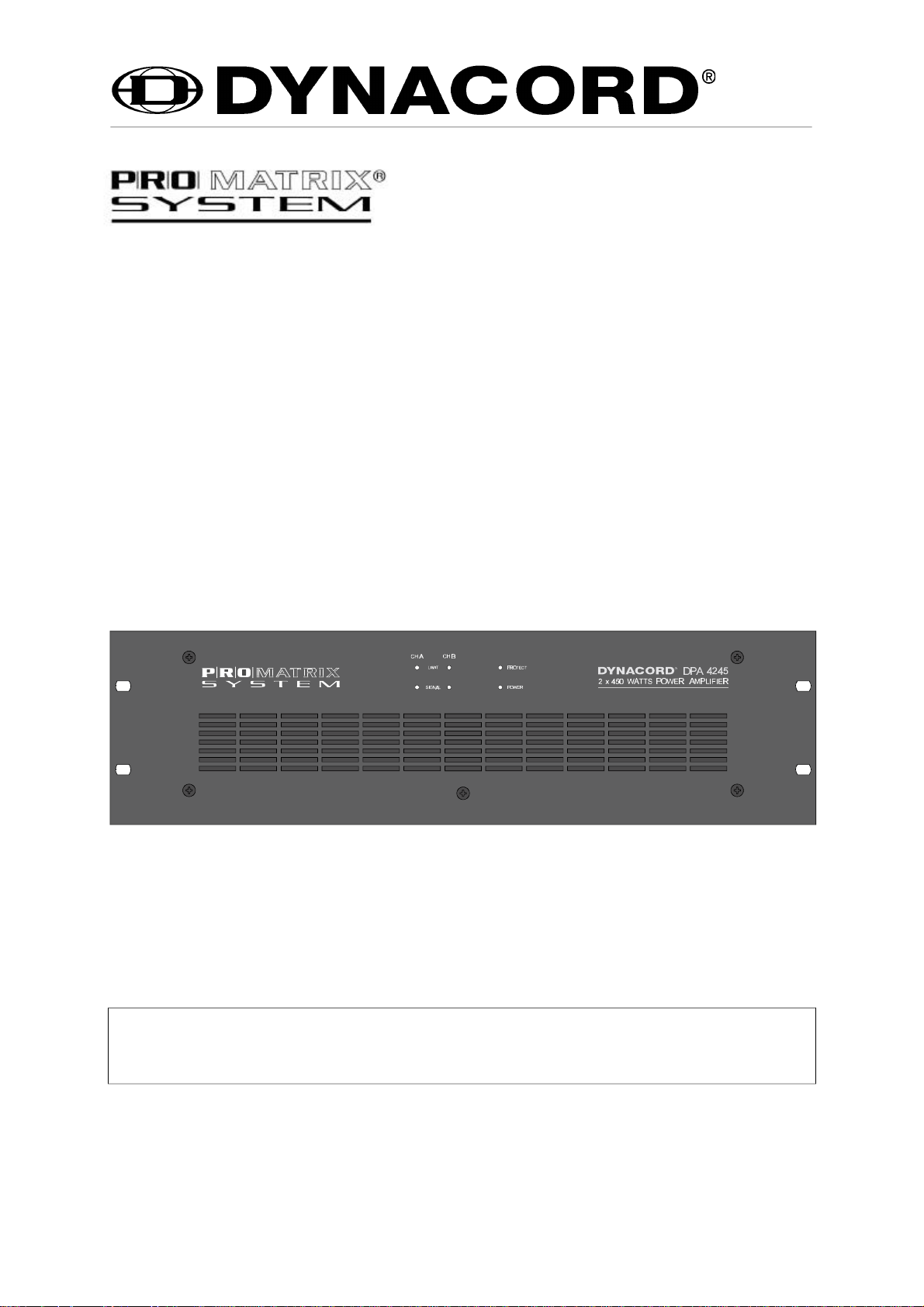
DPA 4245 / DPA 4260 POWER AMPLIFIER
Page 2
MEASUREMENT SPECIFICATIONS: DPA power amplifiers complete appliance
Names of the individual printed board assemblies and their corresponding EDP numbers:
EDP numbers of the main boards
DPA 4245 DPA 4260
84 188 84 189
Board section Index
Main PCB 1
Supply PCB 4
LED PCB 3
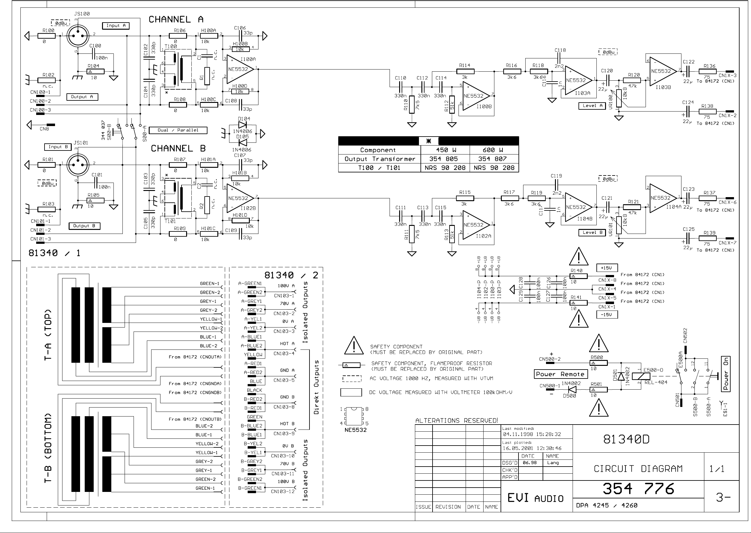
Input-PCB (index 1) and Output-PCB (Index 2) are located on the printed board assembly 81340.
Measuring conditions, unless differently specified:
- measuring tolerance: X = 1.5dB
- measuring frequency: f = 1kHz
- all stated levels refer to: U = 775mV (0dBu)
- level controls are set to their clockwise margin:
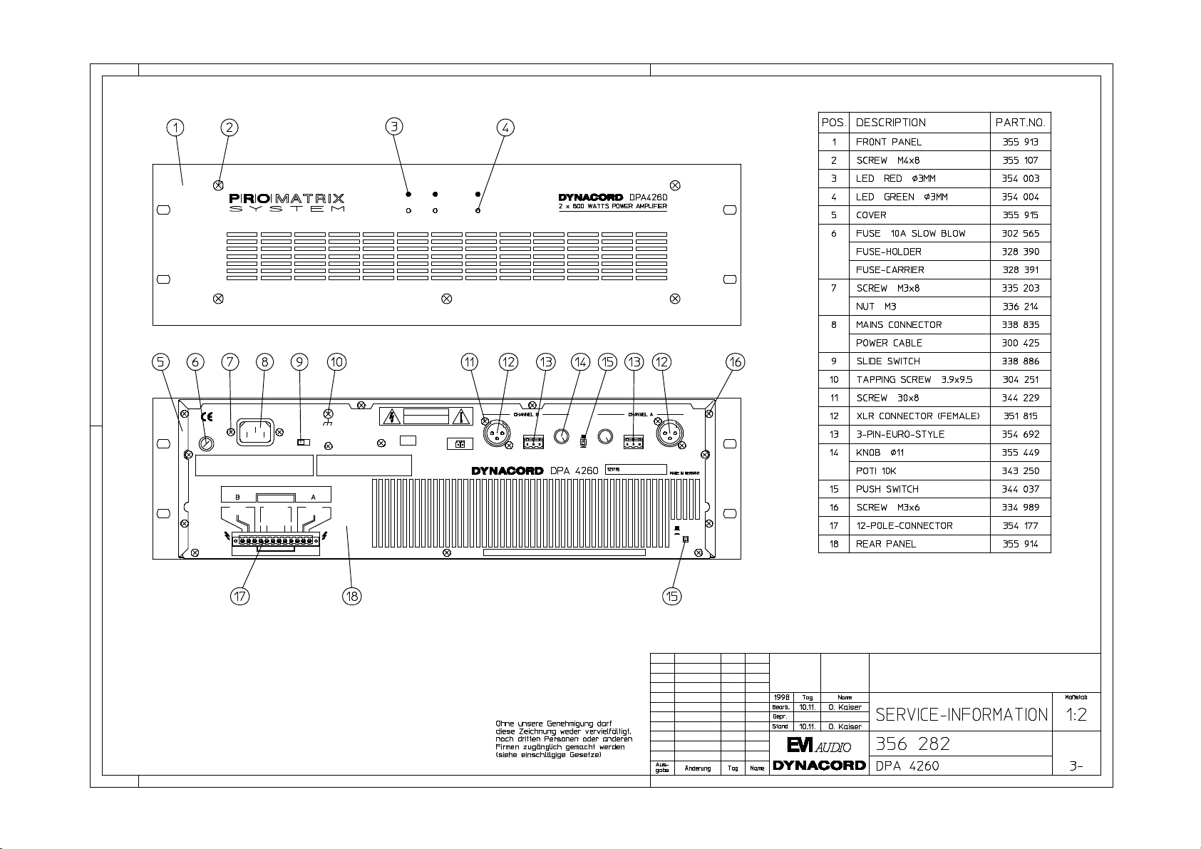
- XLR connector pin-assignment: PIN 1 = GROUND/SHIELD
PIN 2 = + INPUT
PIN 3 = - INPUT
- source impedance for the induction via the XLR-type connector: R(Q) = 50 ohms
- the AMPLIFIER PCB is provided with service connectors:
CNS1 CNS2 CNRC
PIN Assigned to PIN Assigned to PIN Assigned to
1 -Vcc 1 LIM A Switch 1 LIM Out A
2 BIAS +A 2 -15V 2 LIM Out B
3 BIAS -A 3 LIM B Switch 3 Standby via RC
4 FAN Voltage 4 +15V 4 Standby LED
5 +Vcc 5 AGND 5 -Vss
6 BIAS +B 6 Speaker Out A 6 +Vss
7 BIAS -B 7 Relay/Protect 7 n.c.
8 Temp Heatsink 8 Speaker Out B 8 n.c.
- Pin-assignment of the power amplifiers output connector:
PIN Function Channel
1 + pole of the 100V output and + pole of the 25V output
2 - pole of the 25V output and + pole of the 70V output
3 - pole of the 70V output and - pole of the 100V output B
4 + pole Direct Output
5 - pole Direct Output
6,7 not assigned -
8 - pole Direct Output
9 + pole Direct Output
10 - pole of the 70V output and - pole of the 100V output A
11 - pole of the 25V output and + pole of the 70V output
12 + pole of the 100V output and + pole of the 25V output
Pin-assignment of the Power Remote connector: PIN 1 control voltage -
PIN 2 control voltage +
1
Page 3
Nominal load impedances
100V output 70V output 25V output
DPA 4245
DPA 4260
1. Operation voltage: U(B) = 230V / 50Hz ... 60Hz
2. Deviation limit of the operation voltage: -30% .... +10%
3. Power consumption (both channels driven via the 100V output, f = 1kHz)
idling condition power consumption 30-60W 40-80W
nominal power consumption (nominal load) 1580W 1950W
standard power consumption (nominal load) 470W 620W
maximum power consumption (nominal load) 1680W 2180W
power consumption at 1/8 of the maximum output capacity 600W 870W
4. Settings
4.1. IDLING CURRENT ADJUSTMENT
28,5ΩΩ 14ΩΩ 1,8ΩΩ
20ΩΩ 9,8ΩΩ 1,25ΩΩ
DPA 4245 DPA 4260
Connect the DC-volt meter at the BIAS measuring points (refer to service connectors) and adjust the idling
current via the trim potentiometer VR101/VR301 (located on the Main PCB). Adjust both channels of the power
amplifier A&B to U(DC) = 7.5mV. Adjusting the idling current has to be performed at normal room
temperature. In case the power amplifier had previously been operated, it has to be given several hours to regain
its normal temperature.
4.2. VCA - OFFSET
Rhythmically open and short-circuit CNS2.1 and CNS2.2 for channel A as well as CNS2.3 and CNS2.2 for
channel B. The switches are located on the Main PCB. Using VR100 or VR300 respectively to adjust the power
amplifier's Direct Output to its minimum offset (with oscilloscope to minimal peak value or to the audible
minimal volume of the interfering pulse).
5. Functioning test
5.1. OUTPUT - offset voltage
DC-voltage measuring at the Direct Output A/B with U(DC) 10mV.
5.2. LIMITER
5.2.1. Voltage limiter
Both channels separately driven without load via the Direct Output with a 1 kHz signal up to U(A) = 38V.
Increase the input voltage by 10 dB. The LIMITER LED lights and the output voltage ascents by approx. 1.5 dB
or 2.5 dB respectively to approx. 44V or 52V, respectively. The distortion rate of the limited signal should not
ascent above 0.8%.
5.2.2. Distortion limiter
Both channels separately driven via the Direct Output at 2Ω with a 1 kHz signal up to U(A) = 20V or U(A) =
25V, respectively. Increase the input voltage by 5 dB. The LIMITER LED lights and the output voltage ascents
by approx. 1.5dB to approx. 25V or 29V respectively and it is slightly clipping. The distortion rate of the limited
signal is approx. THD = 2 ... 3%. Further increasing the input signal by +10dB should not result in a remarkably
higher clipping of the output signal.
2
Page 4

5.2.3. Attack- and release times
separately testing the power amplifier channels is mandatory: Test has to be performed at the Direct Output
without load.
1.) Drive the power amplifier's input with a burst signal (f = 1kHz, 10 cycles, rate : 3 sec.) and U(E) = +10dBu.
2.) Monitor the output signal via oscilloscope. After 1 - 2 signal periods, the limiter has reduced the major
distortion to a minor residual distortion (THD ≤ 1%)
attack time: approx. 2 ms release time: approx. 130 ms
5.3 POWER-ON DELAY
Feed the test signal to the power amplifier input. Switch the power amplifier ON using the "Power On" switch.
Approximately 2 seconds after pressing the "Power On" switch, the signal is present at the output.
5.4 POWER REMOTE
Switch the power of the appliance OFF. Feed a control voltage of +24V to the Power Remote input. The power
amplifier has to start operation and after disconnecting the control voltage has to go off again.
5.5 FAN CONTROL
Upon powering-on the power amplifier, the fans will run for approximately 2 seconds and stop when the power
amplifier has re-gained its "normal" temperature. In idling condition (power-on, no signal present) the fans are
switched between the SLOW and OFF mode, depending on the heat sink's temperature. Connecting the CNS1.8
via a 5kΩ resistor to +15V lets the fans run in SLOW mode. A FAN VOLTAGE of 16.8V DC can be measured
between pin CNS2.4 and pin CNS1.4. When disconnecting CN5, the fans will run in FAST mode. A FAN
VOLTAGE of 28V DC is measured between pin CNS2.4 and pin CNS1.4.
5.6 SOAR-PROTECTION TEST
Channels separately driven up to 0dB via the Direct-Output, terminated with 4Ω. Parallel connect an 1Ω resistor.
The protection circuit reacts and tries continuously to re-start! The protect-LED lights.
5.7 SHORT-CIRCUIT CURRENT-LIMITING TEST
separately testing the power amplifier channels without load is mandatory:
- drive the channel with a burst signal (f = 1kHz, 1-3 cycles, rate ≈ 1 sec.), at the Direct Output with
U(E) = 0dBu.
- connect a load resistor of 1Ω.
- the short-circuit current-limiter limits the output voltage at the load resistor symmetrically (monitor via
oscilloscope!) to a peak voltage value of 15V or 20V respectively (approx. 15A or 20A respectively maximum
peak output current).
5.8 DC-voltage and HF-Protection Circuit
- Testing the protection circuitry against the occurrence of DC-voltage and HF at the output is only possible
directly via the Main PCB when it is not installed in the appliance.
5.9 INDICATORS TEST
Feed a 1kHz sine signal while slowly increasing the level. At approx. -30dBu the SIGNAL LEDs will light and
at approx. +1.5dBu the Limit LED will light.
3
Page 5
6. Level CHANNEL A B
6.1. VOLTAGE AMPLIFICATION
Appliance Input U(E) Measuring point vU U(A) Load Frequency
DPA 4245 CH. A/B 0dBu Direct Out A/B 33.8dBu 37.8V
DPA 4245 CH. A/B 0dBu 100V Output 42.2dBu 99.2V
DPA 4245 CH. A/B 0dBu 70V Output 39.3dBu 71.6V
4Ω
28.5Ω
14Ω
1kHz
1kHz
1kHz
DPA 4245 CH. A/B 0dBu 25V Output 30.2dBu 25.1V 1.8V 1kHz
DPA 4245 CH. A 0dBu BRIDGED OUT 39.8dBu 76V
DPA 4260 CH. A/B 0dBu Direct Out A/B 34.9dBu 43V
DPA 4260 CH. A/B 0dBu 100V Output 41.8dBu 95.2V
DPA 4260 CH. A/B 0dBu 70V Output 39dBu 68.8V
DPA 4260 CH. A/B 0dBu 25V Output 29.8dBu 24V
DPA 4260 CH. A 0dBu BRIDGED OUT 41dBu 87.3V
8Ω
4Ω
20Ω
9.8Ω
1.25Ω
8Ω
1kHz
1kHz
1kHz
1kHz
1kHz
1kHz
6.2. MAXIMUM INPUT LEVEL: U(E) = +21dBu
7. GROUND LIFT switch
The circuit ground (at the input or the output connector) is measured versus the common ground of the enclosure
(contact at the ground terminal, located on the rear panel - or common ground of the mains cord).
without input transformer GROUNDED : R = 0 Ω with input transformer GROUNDED : R = 0Ω
NOT GROUNDED: R = 5 Ω NOT GROUNDED: R→∞
8. Amplitude - Non-Linearities
- MBW = 80kHz
- all channels terminated with nominal load at nominal power, Direct Output at 8Ω or at 4Ω respectively, at
nominal power
Measurement DPA 4245 DPA 4260 Remarks
100V 70V 25V Direct 100V 70V 25V Direct
THD+N
IMD-SMPTE
DIM 30
<0.1% <0.2% <0.3% <0.05% <0.1% <0.2% <0.3% <0.05%
<0.1% <0.3% <0.5% <0.08% <0.2% <0.3% <0.5% <0.08%
<0.2% <0.2% <0.2% <0.03% <0.2% <0.3% <0.3% <0.03%
1kHz
60Hz, 7kHz
3.15kHz,
15kHz
9. Frequency Response
The frequency response is linear. (mind the border frequencies)
fU -1dB fO -1dB fU -3dB fO -3dB
100V Output 60Hz 17kHz 45Hz 26kHz
70V Output 60Hz 17kHz 45Hz 26kHz
25V Output 60Hz 12kHz 45Hz 22kHz
Direct Output 60Hz 22kHz 45Hz 30kHz
10. Insert Attenuation
Drive the power amplifier in idling condition via the transformer outputs up to the nominal output voltage.
Connect the nominal load and measure the level changes.
DPA 4245 DPA 4260
100V Output
70V Output
25V Output
0,7 dB 0,7 dB
0,8 dB 0,8 dB
1,1 dB 1,1 dB
4
Page 6
11. Crosstalk
It is necessary to align the output transformers when testing the crosstalk. Therefore, turn the transformer outputs
by 90° to each other and both by 45° to the rear panel. Terminate the 100V-outputs with nominal load and feed a
1kHz signal with -10dBu to the B-channel. Measure the crosstalk at the 100V output of the A-channel using a
selective band pass filter and suitable measuring equipment. Turn the upper transformer for minimal reading.
Apply a 1kHz signal with -10dBu at the A-channel and measure the crosstalk at the B-channel. Crosstalk
attenuation on both channels has to at least ≥ 80dB .
12. Noise interference
- U(F) = external voltage un-weighted with B = 22 Hz … 22 kHz, effective value (IEC 268-1)
- U(G) = noise voltage, frequency-weighting filter according to CCIR-468-3, quasi peak weighted (IEC 268-1)
- U(A) = interference voltage A-weighted, dB(A), effective value (IEC 268-1)
- Signal-to-noise ratio referenced to the maximum output voltage at nominal load, A-weighted
- All inputs have to be terminated with 50Ω each; during the noise interference measurement, the outputs have to
be without load
Power amplifier Output U(F)
dBu
LEVEL control up
DPA 4245, 4260 100V -55 -45 -57 -102 100
DPA 4245, 4260 70V -58 -47 -60 -102 100
DPA 4245, 4260 25V -68 -56 -70 -102 100
DPA 4245, 4260 Direct -64 -52 -66 -102 100
LEVEL control down
DPA 4245, 4260 100V -57 -47 -59 - DPA 4245, 4260 70V -59 -50 -61 - DPA 4245, 4260 25V -70 -58 -72 - DPA 4245, 4260 Direct -66 -54 -68 - -
13. Settings when shipped
BRIDGED MODE switch set to NORMAL.
INPUT ROUTING switch set to DUAL/STEREO.
LEVEL control all the way right.
14. Dimensions and Weight
Power amplifier Weight Dimensions in mm
DPA 4245 20.5kg 483 x 132.5 x 385.5
DPA 4260 22.5kg 483 x 132.5 x 385.5
U(G)
dBu
U(A)
dBu
IN(A)
dBu
S/N-R.
dB
5
Page 7

Page 8
Page 9
Page 10

Page 11

Seite / Page 1 / 9
Ersatzteilliste - Bill of Materials
121714
DPA 4245 2X450W VERST.
Pos. Nr.
Best. Nr.
Zubehör
Accessories & packing material
Mechanische Teile
Cabinet material
841888
PCBAR#DPA4245
pcb assy 84188
Ref. No.
G0010 343270 GLRI GBPC 3504 rectifier GBPC-P 3504
Part No. Bezeichnung Description
355871 BEDIENUNGSANL. DPA4245/426 user manual DPA4245/4260
300425 KABEL-NETZ 2.0 M 10A power cable Europe
354179 KABELGEHÄUSE 12POL KGS-MS connector housing
354178 STECKERLEISTE 12POL IC2.5/ connector male 12-pin
354885 BUCHSENLEISTE 2POL connector female 2-pole
354691 BUCHSENLEISTE 3POL connector female 3-pole
332652 KRT. L 2400 612X570X270 carton outer
347526 KRT. IN L 2400 502X465X155 carton inner
303715 STYROPOR-ECK 150X150X150X50 styrofoam #2
348018 SCHUTZFOLIE 1200X800X0,05 poly bag
327495 STYROPOR-ECK 150X150X100X50 styrofoam #1
345438 SCHUTZHÜLLE 165X345X0,05 plastic bag
349988 FALTEINLAGE 750X280 carton filler
349989 FALTEINLAGE 1864X150 carton filler
337059 KNOPF-TASTE 12X7 SW 3.3 push button black 12x7
357958 DK 11 SW/WS/RT C 6FL rotary knob
348415 LÜFTER TYP FBAO8A24H DC fan dc 24V
349693 KABEL-KONFEKT 4POL 0.670M ribbon cable assy 4-way
346790 KABEL-KONFEKT 8POL 0.300M ribbon cable assy 8way
349691 KABEL-KONFEKT 8POL 0.440M ribbon cable assy 8way
355873 FB.DPA4245 BED front panel DPA4245
355915 DEC.3HE DPA4245,4260 top cover
354549 NT-RG.Q44/S900/CPS1 230V power transformer 230V
348805 WI-SO PTC K155 100GRAD safety component PTC
348341 FEDERLEISTE 3POL CE100- connector female 3-pole
354805 ÜT-RG.DPA4245 100V output transformer 100V
348341 FEDERLEISTE 3POL CE100- connector female 3-pole
CNAC1 343516 FL.STECKER 4.8/0.5 connector 4.8mm faston
CNAC2 343516 FL.STECKER 4.8/0.5 connector 4.8mm faston
CNGND 343516 FL.STECKER 4.8/0.5 connector 4.8mm faston
CNGN1 330269 FL.STECKER 6.3/0.8 connector 6.3mm faston
CN001 344862 MESSERLST. 8POL connector male 8-pin
CN002 348334 STIFTLEISTE 3POL MLSS connector male 3-pin
CN003 348334 STIFTLEISTE 3POL MLSS connector male 3-pin
CN005 348334 STIFTLEISTE 3POL MLSS connector male 3-pin
CN007 330269 FL.STECKER 6.3/0.8 connector 6.3mm faston
CN010 330269 FL.STECKER 6.3/0.8 connector 6.3mm faston
CN013 330269 FL.STECKER 6.3/0.8 connector 6.3mm faston
CN018 341937 MESSERLST. 4POL connector male 4-pin
CN019 330269 FL.STECKER 6.3/0.8 connector 6.3mm faston
Page 12

Seite / Page 2 / 9
121714
DPA 4245 2X450W VERST.
Pos. Nr.
Best. Nr.
Ref. No.
CN020 344862 MESSERLST. 8POL connector male 8-pin
CN08X 343516 FL.STECKER 4.8/0.5 connector 4.8mm faston
CN18X 341937 MESSERLST. 4POL connector male 4-pin
CN20X 344862 MESSERLST. 8POL connector male 8-pin
C0001 342923 KO-FOL 0.220MF 63V 5% cap mylar 220nF
C0002 307445 KO-EL 10.000MF 35V cap electrolytic 10uF/35V
C0005 329021 KO-KER 0.10MF 100V 20% cap ceramic 100nF
C0006 329021 KO-KER 0.10MF 100V 20% cap ceramic 100nF
C0007 343530 KO-EL 47.000MF 50V cap electrolytic 47uF/50V
C0008 329021 KO-KER 0.10MF 100V 20% cap ceramic 100nF
C0011 351835 KO-EL 4700.000MF 100V 20% cap electrolytic 4700uF/100
C0012 351835 KO-EL 4700.000MF 100V 20% cap electrolytic 4700uF/100
C0013 351835 KO-EL 4700.000MF 100V 20% cap electrolytic 4700uF/100
C0014 351835 KO-EL 4700.000MF 100V 20% cap electrolytic 4700uF/100
C0015 341714 KO-SO 0.10MF 275V 20% K safety cap 100nF/275V
C0016 329021 KO-KER 0.10MF 100V 20% cap ceramic 100nF
C0017 329021 KO-KER 0.10MF 100V 20% cap ceramic 100nF
C0018 327366 KO-EL 4.700MF 50V BIP cap bip electr. 4.7uF/50V
C0019 329021 KO-KER 0.10MF 100V 20% cap ceramic 100nF
C0022 329021 KO-KER 0.10MF 100V 20% cap ceramic 100nF
C0023 329021 KO-KER 0.10MF 100V 20% cap ceramic 100nF
C0024 335935 KO-EL 2200.000MF 35V cap electrolytic 2200uF/35V
C0025 335935 KO-EL 2200.000MF 35V cap electrolytic 2200uF/35V
C0026 343530 KO-EL 47.000MF 50V cap electrolytic 47uF/50V
C0027 343530 KO-EL 47.000MF 50V cap electrolytic 47uF/50V
C0028 301524 KO-KER 47.0PF 500V 10% cap ceramic 47pF
C0029 301524 KO-KER 47.0PF 500V 10% cap ceramic 47pF
C0030 329021 KO-KER 0.10MF 100V 20% cap ceramic 100nF
C0031 329021 KO-KER 0.10MF 100V 20% cap ceramic 100nF
C0032 341714 KO-SO 0.10MF 275V 20% K safety cap 100nF/275V
C0100 301558 KO-KER 33.0PF 100V 2% cap ceramic 33pF
C0101 301558 KO-KER 33.0PF 100V 2% cap ceramic 33pF
C0102 301478 KO-EL 22.000MF 63V cap electrolytic 22uF/63V
C0103 335787 KO-KER 15.0PF 100V 2% cap ceramic 15pF
C0104 335787 KO-KER 15.0PF 100V 2% cap ceramic 15pF
C0105 301458 KO-EL 2.200MF 63V cap electrolytic 2.2uF/63V
C0106 327390 KO-FOL 470.000PF 100V 5% cap mylar 470pF
C0107 340988 KO-FOL 0.470MF 63V 5% cap mylar 470nF
C0108 301530 KO-KER 100.0PF 500V 10% cap ceramic 100pF
C0109 343532 KO-EL 100.000MF 25V cap electrolytic 100uF/25V
C0110 343532 KO-EL 100.000MF 25V cap electrolytic 100uF/25V
C0111 340988 KO-FOL 0.470MF 63V 5% cap mylar 470nF
C0112 343532 KO-EL 100.000MF 25V cap electrolytic 100uF/25V
C0113 343532 KO-EL 100.000MF 25V cap electrolytic 100uF/25V
C0114 329021 KO-KER 0.10MF 100V 20% cap ceramic 100nF
C0115 329021 KO-KER 0.10MF 100V 20% cap ceramic 100nF
C0116 343532 KO-EL 100.000MF 25V cap electrolytic 100uF/25V
C0117 351994 KO-KER 120.0PF 500V 2% cap ceramic 120pF
C0118 351994 KO-KER 120.0PF 500V 2% cap ceramic 120pF
C0119 343531 KO-EL 47.000MF 63V cap electrolytic 47uF/63V
C0120 341714 KO-SO 0.10MF 275V 20% K safety cap 100nF/275V
C0123 301519 KO-KER 10.0PF 500V 10% cap ceramic 10pF
Part No. Bezeichnung Description
Page 13

Seite / Page 3 / 9
121714
DPA 4245 2X450W VERST.
Pos. Nr.
Best. Nr.
Ref. No.
C0124 301519 KO-KER 10.0PF 500V 10% cap ceramic 10pF
C0125 301474 KO-EL 22.000MF 16V BIP cap bip electr. 22uF/16V
C0126 329021 KO-KER 0.10MF 100V 20% cap ceramic 100nF
C0127 329021 KO-KER 0.10MF 100V 20% cap ceramic 100nF
C0128 329021 KO-KER 0.10MF 100V 20% cap ceramic 100nF
C0129 329021 KO-KER 0.10MF 100V 20% cap ceramic 100nF
C0300 301558 KO-KER 33.0PF 100V 2% cap ceramic 33pF
C0301 301558 KO-KER 33.0PF 100V 2% cap ceramic 33pF
C0302 301478 KO-EL 22.000MF 63V cap electrolytic 22uF/63V
C0303 335787 KO-KER 15.0PF 100V 2% cap ceramic 15pF
C0304 335787 KO-KER 15.0PF 100V 2% cap ceramic 15pF
C0305 301458 KO-EL 2.200MF 63V cap electrolytic 2.2uF/63V
C0306 327390 KO-FOL 470.000PF 100V 5% cap mylar 470pF
C0307 340988 KO-FOL 0.470MF 63V 5% cap mylar 470nF
C0308 301530 KO-KER 100.0PF 500V 10% cap ceramic 100pF
C0309 343532 KO-EL 100.000MF 25V cap electrolytic 100uF/25V
C0310 343532 KO-EL 100.000MF 25V cap electrolytic 100uF/25V
C0311 340988 KO-FOL 0.470MF 63V 5% cap mylar 470nF
C0312 343532 KO-EL 100.000MF 25V cap electrolytic 100uF/25V
C0313 343532 KO-EL 100.000MF 25V cap electrolytic 100uF/25V
C0314 329021 KO-KER 0.10MF 100V 20% cap ceramic 100nF
C0315 329021 KO-KER 0.10MF 100V 20% cap ceramic 100nF
C0316 343532 KO-EL 100.000MF 25V cap electrolytic 100uF/25V
C0317 351994 KO-KER 120.0PF 500V 2% cap ceramic 120pF
C0318 351994 KO-KER 120.0PF 500V 2% cap ceramic 120pF
C0319 343531 KO-EL 47.000MF 63V cap electrolytic 47uF/63V
C0320 341714 KO-SO 0.10MF 275V 20% K safety cap 100nF/275V
C0323 301519 KO-KER 10.0PF 500V 10% cap ceramic 10pF
C0324 301519 KO-KER 10.0PF 500V 10% cap ceramic 10pF
C0325 301474 KO-EL 22.000MF 16V BIP cap bip electr. 22uF/16V
C0326 329021 KO-KER 0.10MF 100V 20% cap ceramic 100nF
C0327 329021 KO-KER 0.10MF 100V 20% cap ceramic 100nF
C0328 329021 KO-KER 0.10MF 100V 20% cap ceramic 100nF
C0329 329021 KO-KER 0.10MF 100V 20% cap ceramic 100nF
C0519 329021 KO-KER 0.10MF 100V 20% cap ceramic 100nF
C0520 340522 KO-EL 10.000MF 35V cap electrolytic 10uF/35
C0521 340522 KO-EL 10.000MF 35V cap electrolytic 10uF/35
D0002 304360 DIODE 1N 4007 GEGURTET diode 1N 4002
D0003 301254 DIODE 1N 4148 AXIAL diode 1N 4148
D0004 301254 DIODE 1N 4148 AXIAL diode 1N 4148
D0005 301254 DIODE 1N 4148 AXIAL diode 1N 4148
D0006 301254 DIODE 1N 4148 AXIAL diode 1N 4148
D0007 301254 DIODE 1N 4148 AXIAL diode 1N 4148
D0008 301254 DIODE 1N 4148 AXIAL diode 1N 4148
D0009 304360 DIODE 1N 4007 GEGURTET diode 1N 4002
D0010 301254 DIODE 1N 4148 AXIAL diode 1N 4148
D0011 301254 DIODE 1N 4148 AXIAL diode 1N 4148
D0014 301254 DIODE 1N 4148 AXIAL diode 1N 4148
D0015 301254 DIODE 1N 4148 AXIAL diode 1N 4148
D0016 304360 DIODE 1N 4007 GEGURTET diode 1N 4002
D0017 304360 DIODE 1N 4007 GEGURTET diode 1N 4002
D0018 304360 DIODE 1N 4007 GEGURTET diode 1N 4002
Part No. Bezeichnung Description
Page 14

Seite / Page 4 / 9
121714
DPA 4245 2X450W VERST.
Pos. Nr.
Best. Nr.
Ref. No.
D0019 304360 DIODE 1N 4007 GEGURTET diode 1N 4002
D0020 304992 DIODZ BZX 55C 6V8 0.50W diode zener 6V8
D0021 304992 DIODZ BZX 55C 6V8 0.50W diode zener 6V8
D0022 304360 DIODE 1N 4007 GEGURTET diode 1N 4002
D0023 304360 DIODE 1N 4007 GEGURTET diode 1N 4002
D0100 301254 DIODE 1N 4148 AXIAL diode 1N 4148
D0101 301254 DIODE 1N 4148 AXIAL diode 1N 4148
D0102 301254 DIODE 1N 4148 AXIAL diode 1N 4148
D0104 329511 DIODZ BZX 55C 2V4 0.50W diode zener 2V4
D0105 309450 DIODZ BZX 55C 15V 0.50W diode zener 15V
D0106 309450 DIODZ BZX 55C 15V 0.50W diode zener 15V
D0107 301254 DIODE 1N 4148 AXIAL diode 1N 4148
D0108 301254 DIODE 1N 4148 AXIAL diode 1N 4148
D0109 301254 DIODE 1N 4148 AXIAL diode 1N 4148
D0110 301254 DIODE 1N 4148 AXIAL diode 1N 4148
D0111 307916 DIODZ BZX 55C 7V5 0.50W diode zener 7V5
D0112 307916 DIODZ BZX 55C 7V5 0.50W diode zener 7V5
D0113 301254 DIODE 1N 4148 AXIAL diode 1N 4148
D0114 304360 DIODE 1N 4007 GEGURTET diode 1N 4002
D0115 304360 DIODE 1N 4007 GEGURTET diode 1N 4002
D0116 301254 DIODE 1N 4148 AXIAL diode 1N 4148
D0117 301254 DIODE 1N 4148 AXIAL diode 1N 4148
D0118 354804 DIODZ ZPY 62V 1.30W diode zener 62V
D0119 354804 DIODZ ZPY 62V 1.30W diode zener 62V
D0300 301254 DIODE 1N 4148 AXIAL diode 1N 4148
D0301 301254 DIODE 1N 4148 AXIAL diode 1N 4148
D0302 301254 DIODE 1N 4148 AXIAL diode 1N 4148
D0304 329511 DIODZ BZX 55C 2V4 0.50W diode zener 2V4
D0305 309450 DIODZ BZX 55C 15V 0.50W diode zener 15V
D0306 309450 DIODZ BZX 55C 15V 0.50W diode zener 15V
D0307 301254 DIODE 1N 4148 AXIAL diode 1N 4148
D0308 301254 DIODE 1N 4148 AXIAL diode 1N 4148
D0309 301254 DIODE 1N 4148 AXIAL diode 1N 4148
D0310 301254 DIODE 1N 4148 AXIAL diode 1N 4148
D0311 307916 DIODZ BZX 55C 7V5 0.50W diode zener 7V5
D0312 307916 DIODZ BZX 55C 7V5 0.50W diode zener 7V5
D0313 301254 DIODE 1N 4148 AXIAL diode 1N 4148
D0314 304360 DIODE 1N 4007 GEGURTET diode 1N 4002
D0315 304360 DIODE 1N 4007 GEGURTET diode 1N 4002
D0316 301254 DIODE 1N 4148 AXIAL diode 1N 4148
D0317 301254 DIODE 1N 4148 AXIAL diode 1N 4148
D0318 354804 DIODZ ZPY 62V 1.30W diode zener 62V
D0319 354804 DIODZ ZPY 62V 1.30W diode zener 62V
D0503 354004 LED GN 3MM LOW CURRENT led green
D0504 354003 LED RT 3MM LOW CURRENT led red
D0505 354003 LED RT 3MM LOW CURRENT led red
D0508 354003 LED RT 3MM LOW CURRENT led red
D0509 301254 DIODE 1N 4148 AXIAL diode 1N 4148
D0510 354004 LED GN 3MM LOW CURRENT led green
D0511 354004 LED GN 3MM LOW CURRENT led green
D0512 301254 DIODE 1N 4148 AXIAL diode 1N 4148
E0001 354859 RELAIS 793-P-1C-S-24V DC relay 24V
Part No. Bezeichnung Description
Page 15

Seite / Page 5 / 9
121714
DPA 4245 2X450W VERST.
Pos. Nr.
Best. Nr.
Ref. No.
E0100 354859 RELAIS 793-P-1C-S-24V DC relay 24V
E0300 354859 RELAIS 793-P-1C-S-24V DC relay 24V
F0001 302582 SICHER T 1 A 250V fuse 1A slow blow
F0002 302582 SICHER T 1 A 250V fuse 1A slow blow
F0003 332065 SICHER T 8 A 250V fuse 8A slow blow
H0100 343456 DICKS-NETZW. 8PIN 2% res.network 8x4k7
H0101 343457 DICKS-NETZW. 8PIN 2% res.network 8x10k
H0300 343456 DICKS-NETZW. 8PIN 2% res.network 8x4k7
H0301 343457 DICKS-NETZW. 8PIN 2% res.network 8x10k
I0001 332985 IC TL 074 CN IC TL 074 CN
I0100 327197 IC NE 5532 P 2FACH OP IC NE 5532 N
I0101 307421 IC CA 3080 E OTA IC CA 3080 E
I0102 332985 IC TL 074 CN IC TL 074 CN
I0103 338359 IC LM 308 AN IC LM 308 A
I0300 327197 IC NE 5532 P 2FACH OP IC NE 5532 N
I0301 307421 IC CA 3080 E OTA IC CA 3080 E
I0302 332985 IC TL 074 CN IC TL 074 CN
I0303 338359 IC LM 308 AN IC LM 308 A
JS001 338835 STECKER-KALTGERÄTE connector male mains
L0100 348592 FILTERSP. 2.50UH/0.004OHM coil 2.5uH
L0300 348592 FILTERSP. 2.50UH/0.004OHM coil 2.5uH
Q0001 306928 TRANS BC 560 C transistor BC 560 C
Q0002 306928 TRANS BC 560 C transistor BC 560 C
Q0003 306928 TRANS BC 560 C transistor BC 560 C
Q0004 306928 TRANS BC 560 C transistor BC 560 C
Q0005 306928 TRANS BC 560 C transistor BC 560 C
Q0008 307150 TRANS BC 337-25 TO 92 transistor BC 337-25
Q0009 301184 TRANS BC 550 C transistor BC 550 B
Q0010 348591 TRANS BC 618 DARL. TO 92 transistor BC 618
Q0011 301184 TRANS BC 550 C transistor BC 550 B
Q0012 307150 TRANS BC 337-25 TO 92 transistor BC 337-25
Q0017 307150 TRANS BC 337-25 TO 92 transistor BC 337-25
Q0018 307430 TRANS BC 327-25 TO 92 transistor BC 327-25
Q0019 307430 TRANS BC 327-25 TO 92 transistor BC 327-25
Q0020 301235 TRANS BD 242 B transistor BD 242 B
Q0021 307150 TRANS BC 337-25 TO 92 transistor BC 337-25
Q0022 301236 TRANS BD 241 B transistor BD 241 B
Q0023 307150 TRANS BC 337-25 TO 92 transistor BC 337-25
Q0100 348421 TRANS 2N 3906 transistor 2N 3906
Q0101 335763 TRANS 2N 3904 transistor 2N 3904
Q0103 330264 TRANS J 111 transistor J 111 A
Q0104 335763 TRANS 2N 3904 transistor 2N 3904
Q0105 348421 TRANS 2N 3906 transistor 2N 3906
Q0106 348422 TRANS MPSA 42 transistor MPSA 42
Q0107 348423 TRANS MPSA 92 transistor MPSA 92
Q0108 335763 TRANS 2N 3904 transistor 2N 3904
Q0109 348421 TRANS 2N 3906 transistor 2N 3906
Q0110 348422 TRANS MPSA 42 transistor MPSA 42
Q0111 348423 TRANS MPSA 92 transistor MPSA 92
Q0112 335763 TRANS 2N 3904 transistor 2N 3904
Q0113 348421 TRANS 2N 3906 transistor 2N 3906
Q0114 335763 TRANS 2N 3904 transistor 2N 3904
Part No. Bezeichnung Description
Page 16

Seite / Page 6 / 9
121714
DPA 4245 2X450W VERST.
Pos. Nr.
Best. Nr.
Ref. No.
Q0115 348421 TRANS 2N 3906 transistor 2N 3906
00010 338869 TRANS MJE 350 transistor MJE 350
00010 338868 TRANS MJE 340 transistor MJE 340
Q0118 348409 TRANS 2SC 4793 transistor 2SC 4793
Q0119 348421 TRANS 2N 3906 transistor 2N 3906
Q0120 335763 TRANS 2N 3904 transistor 2N 3904
Q0121 335763 TRANS 2N 3904 transistor 2N 3904
Q0122 348421 TRANS 2N 3906 transistor 2N 3906
Q0123 351981 TRANS MJL 3281 A transistor MJL 3281 A
Q0124 351982 TRANS MJL 1302 A transistor MJL 1302 A
Q0125 331657 TRANS MJ 15022 transistor MJ 15022
Q0126 331658 TRANS MJ 15023 transistor MJ 15023
Q0127 331657 TRANS MJ 15022 transistor MJ 15022
Q0128 331658 TRANS MJ 15023 transistor MJ 15023
Q0129 331657 TRANS MJ 15022 transistor MJ 15022
Q0130 331658 TRANS MJ 15023 transistor MJ 15023
Q0131 331657 TRANS MJ 15022 transistor MJ 15022
Q0132 331658 TRANS MJ 15023 transistor MJ 15023
Q0135 348422 TRANS MPSA 42 transistor MPSA 42
Q0136 348423 TRANS MPSA 92 transistor MPSA 92
Q0137 348423 TRANS MPSA 92 transistor MPSA 92
Q0138 348422 TRANS MPSA 42 transistor MPSA 42
Q0139 307911 TRANS BF 393 transistor BF 391
Q0140 307911 TRANS BF 393 transistor BF 391
Q0141 348423 TRANS MPSA 92 transistor MPSA 92
Q0142 348423 TRANS MPSA 92 transistor MPSA 92
Q0143 348421 TRANS 2N 3906 transistor 2N 3906
Q0144 348421 TRANS 2N 3906 transistor 2N 3906
Q0145 335763 TRANS 2N 3904 transistor 2N 3904
Q0146 306928 TRANS BC 560 C transistor BC 560 C
Q0300 348421 TRANS 2N 3906 transistor 2N 3906
Q0301 335763 TRANS 2N 3904 transistor 2N 3904
Q0303 330264 TRANS J 111 transistor J 111 A
Q0304 335763 TRANS 2N 3904 transistor 2N 3904
Q0305 348421 TRANS 2N 3906 transistor 2N 3906
Q0306 348422 TRANS MPSA 42 transistor MPSA 42
Q0307 348423 TRANS MPSA 92 transistor MPSA 92
Q0308 335763 TRANS 2N 3904 transistor 2N 3904
Q0309 348421 TRANS 2N 3906 transistor 2N 3906
Q0310 348422 TRANS MPSA 42 transistor MPSA 42
Q0311 348423 TRANS MPSA 92 transistor MPSA 92
Q0312 335763 TRANS 2N 3904 transistor 2N 3904
Q0313 348421 TRANS 2N 3906 transistor 2N 3906
Q0314 335763 TRANS 2N 3904 transistor 2N 3904
Q0315 348421 TRANS 2N 3906 transistor 2N 3906
00010 338869 TRANS MJE 350 transistor MJE 350
00010 338868 TRANS MJE 340 transistor MJE 340
Q0318 348409 TRANS 2SC 4793 transistor 2SC 4793
Q0319 348421 TRANS 2N 3906 transistor 2N 3906
Q0320 335763 TRANS 2N 3904 transistor 2N 3904
Q0321 335763 TRANS 2N 3904 transistor 2N 3904
Q0322 348421 TRANS 2N 3906 transistor 2N 3906
Part No. Bezeichnung Description
Page 17

Seite / Page 7 / 9
121714
DPA 4245 2X450W VERST.
Pos. Nr.
Best. Nr.
Ref. No.
Q0323 351981 TRANS MJL 3281 A transistor MJL 3281 A
Q0324 351982 TRANS MJL 1302 A transistor MJL 1302 A
Q0327 331657 TRANS MJ 15022 transistor MJ 15022
Q0328 331658 TRANS MJ 15023 transistor MJ 15023
Q0329 331657 TRANS MJ 15022 transistor MJ 15022
Q0330 331658 TRANS MJ 15023 transistor MJ 15023
Q0331 331657 TRANS MJ 15022 transistor MJ 15022
Q0332 331658 TRANS MJ 15023 transistor MJ 15023
Q0333 331657 TRANS MJ 15022 transistor MJ 15022
Q0334 331658 TRANS MJ 15023 transistor MJ 15023
Q0335 348422 TRANS MPSA 42 transistor MPSA 42
Q0336 348423 TRANS MPSA 92 transistor MPSA 92
Q0337 348423 TRANS MPSA 92 transistor MPSA 92
Q0338 348422 TRANS MPSA 42 transistor MPSA 42
Q0339 307911 TRANS BF 393 transistor BF 391
Q0340 307911 TRANS BF 393 transistor BF 391
Q0341 348423 TRANS MPSA 92 transistor MPSA 92
Q0342 348423 TRANS MPSA 92 transistor MPSA 92
Q0343 348421 TRANS 2N 3906 transistor 2N 3906
Q0344 348421 TRANS 2N 3906 transistor 2N 3906
Q0345 335763 TRANS 2N 3904 transistor 2N 3904
Q0346 306928 TRANS BC 560 C transistor BC 560 C
Q0501 306928 TRANS BC 560 C transistor BC 560 C
Q0502 348422 TRANS MPSA 42 transistor MPSA 42
Q0503 348422 TRANS MPSA 42 transistor MPSA 42
Q0504 301184 TRANS BC 550 C transistor BC 550 B
Q0505 301184 TRANS BC 550 C transistor BC 550 B
Q0506 306928 TRANS BC 560 C transistor BC 560 C
Q0507 306928 TRANS BC 560 C transistor BC 560 C
R0037 348490 WI-SO NTC K 164/100K/J safety component NTC
R0065 348550 WI-SO NTC 10 OHM K safety resistor 10 Ohm
R0185 348456 WI-DR 2X 0.22 OHM 5.00W 5% resistor 2x0.22 Ohm 5watt
R0188 348456 WI-DR 2X 0.22 OHM 5.00W 5% resistor 2x0.22 Ohm 5watt
R0191 348456 WI-DR 2X 0.22 OHM 5.00W 5% resistor 2x0.22 Ohm 5watt
R0194 348456 WI-DR 2X 0.22 OHM 5.00W 5% resistor 2x0.22 Ohm 5watt
R0208 348593 WI-SO NTC K 164/2.2K safety component NTC
R0209 348593 WI-SO NTC K 164/2.2K safety component NTC
R0223 341713 WI-DR 4.70 OHM 4.00W 5% resistor 4.70 Ohm 4watt
R0225 341713 WI-DR 4.70 OHM 4.00W 5% resistor 4.70 Ohm 4watt
R0227 341713 WI-DR 4.70 OHM 4.00W 5% resistor 4.70 Ohm 4watt
R0388 348456 WI-DR 2X 0.22 OHM 5.00W 5% resistor 2x0.22 Ohm 5watt
R0391 348456 WI-DR 2X 0.22 OHM 5.00W 5% resistor 2x0.22 Ohm 5watt
R0394 348456 WI-DR 2X 0.22 OHM 5.00W 5% resistor 2x0.22 Ohm 5watt
R0397 348456 WI-DR 2X 0.22 OHM 5.00W 5% resistor 2x0.22 Ohm 5watt
R0408 348593 WI-SO NTC K 164/2.2K safety component NTC
R0409 348593 WI-SO NTC K 164/2.2K safety component NTC
R0423 341713 WI-DR 4.70 OHM 4.00W 5% resistor 4.70 Ohm 4watt
R0425 341713 WI-DR 4.70 OHM 4.00W 5% resistor 4.70 Ohm 4watt
R0427 341713 WI-DR 4.70 OHM 4.00W 5% resistor 4.70 Ohm 4watt
S0001 344037 SCHALTER-RAST 2XUM switch dpdt latching
S0002 338886 SCHALTER-SCHIEBE L202-02-1- switch slide
VR100 348486 WI-TRI 47.00 KOHM LIN pot trim 47k Ohm lin
Part No. Bezeichnung Description
Page 18

Seite / Page 8 / 9
121714
DPA 4245 2X450W VERST.
Pos. Nr.
Best. Nr.
813408
PCB-A:DPA4245/4260 N 5
pcb assy 81340
Ref. No.
VR101 348674 WI-TRI 250.00 OHM LIN pot trim 250 Ohm lin
VR300 348486 WI-TRI 47.00 KOHM LIN pot trim 47k Ohm lin
VR301 348674 WI-TRI 250.00 OHM LIN pot trim 250 Ohm lin
00030 303576 SICHER-HALTE-FEDER fuse clip
00035 328390 SICHER-HALTER FAU fuse holder
00040 328391 SICHER-HALTER-KAPPE FEK fuse holder carrier
00075 354306 STIFTLEISTE 16POL connector male 16-pin
CN01X 344862 MESSERLST. 8POL connector male 8-pin
CN100 354692 STIFTLEISTE 3POL connector male 3-pin
CN101 354692 STIFTLEISTE 3POL connector male 3-pin
CN103 354177 BUCHSENLEISTE 12POL connector female 12-pole
CN500 354886 STIFTLEISTE 2POL MC1.5/ 2 connector male 2-pole
C0100 329021 KO-KER 0.10MF 100V 20% cap ceramic 100nF
C0101 329021 KO-KER 0.10MF 100V 20% cap ceramic 100nF
C0102 301543 KO-KER 330.0PF 500V 10% cap ceramic 330pF
C0103 301543 KO-KER 330.0PF 500V 10% cap ceramic 330pF
C0104 301543 KO-KER 330.0PF 500V 10% cap ceramic 330pF
C0105 301543 KO-KER 330.0PF 500V 10% cap ceramic 330pF
C0106 301558 KO-KER 33.0PF 100V 2% cap ceramic 33pF
C0107 301558 KO-KER 33.0PF 100V 2% cap ceramic 33pF
C0108 301558 KO-KER 33.0PF 100V 2% cap ceramic 33pF
C0109 301558 KO-KER 33.0PF 100V 2% cap ceramic 33pF
C0110 340244 KO-FOL 0.330MF 63V 5% cap mylar 330nF
C0111 340244 KO-FOL 0.330MF 63V 5% cap mylar 330nF
C0112 340244 KO-FOL 0.330MF 63V 5% cap mylar 330nF
C0113 340244 KO-FOL 0.330MF 63V 5% cap mylar 330nF
C0114 340244 KO-FOL 0.330MF 63V 5% cap mylar 330nF
C0115 340244 KO-FOL 0.330MF 63V 5% cap mylar 330nF
C0116 343397 KO-FOL 1000.000PF 100V2.5% cap mylar 1nF
C0117 343397 KO-FOL 1000.000PF 100V2.5% cap mylar 1nF
C0118 326924 KO-FOL 2200.000PF 100V 5% cap mylar 2200pF
C0119 326924 KO-FOL 2200.000PF 100V 5% cap mylar 2200pF
C0120 340523 KO-EL 22.000MF 16V cap electrolytic 22uF/16V
C0121 340523 KO-EL 22.000MF 16V cap electrolytic 22uF/16V
C0122 340523 KO-EL 22.000MF 16V cap electrolytic 22uF/16V
C0123 340523 KO-EL 22.000MF 16V cap electrolytic 22uF/16V
C0124 340523 KO-EL 22.000MF 16V cap electrolytic 22uF/16V
C0125 340523 KO-EL 22.000MF 16V cap electrolytic 22uF/16V
C0126 329021 KO-KER 0.10MF 100V 20% cap ceramic 100nF
C0127 329021 KO-KER 0.10MF 100V 20% cap ceramic 100nF
C0128 329021 KO-KER 0.10MF 100V 20% cap ceramic 100nF
C0129 329021 KO-KER 0.10MF 100V 20% cap ceramic 100nF
D0104 304360 DIODE 1N 4007 GEGURTET diode 1N 4002
D0105 304360 DIODE 1N 4007 GEGURTET diode 1N 4002
D0500 304360 DIODE 1N 4007 GEGURTET diode 1N 4002
D0501 304360 DIODE 1N 4007 GEGURTET diode 1N 4002
E0500 356594 RELAIS 793-P-1A-S-TV10 relay
H0100 343457 DICKS-NETZW. 8PIN 2% res.network 8x10k
H0101 343457 DICKS-NETZW. 8PIN 2% res.network 8x10k
Part No. Bezeichnung Description
Page 19

Seite / Page 9 / 9
121714
DPA 4245 2X450W VERST.
Pos. Nr.
Best. Nr.
Ref. No.
I0100 327197 IC NE 5532 P 2FACH OP IC NE 5532 N
I0102 327197 IC NE 5532 P 2FACH OP IC NE 5532 N
I0103 327197 IC NE 5532 P 2FACH OP IC NE 5532 N
I0104 327197 IC NE 5532 P 2FACH OP IC NE 5532 N
JS100 351815 BUCHSE-FL. XLR 3POL SW xlr connector female 3-pole
JS101 351815 BUCHSE-FL. XLR 3POL SW xlr connector female 3-pole
S0100 344037 SCHALTER-RAST 2XUM switch dpdt latching
S0500 349114 SCHALTER-NETZ mains switch
VR100 343250 P-DREH 10KOHM LIN B potentiometer 10kohm lin
VR101 343250 P-DREH 10KOHM LIN B potentiometer 10kohm lin
00010 330269 FL.STECKER 6.3/0.8 connector 6.3mm faston
Part No. Bezeichnung Description
Page 20

Seite / Page 1 / 9
Ersatzteilliste - Bill of Materials
121715
DPA 4260 2X600W VERST.
Pos. Nr.
Best. Nr.
Zubehör
Accessories & packing material
Mechanische Teile
Cabinet material
841898
PCBAR#DPA4260
pcb assy 84189
Ref. No.
G0010 343270 GLRI GBPC 3504 rectifier GBPC-P 3504
Part No. Bezeichnung Description
355871 BEDIENUNGSANL. DPA4245/426 user manual DPA4245/4260
300425 KABEL-NETZ 2.0 M 10A power cable Europe
354179 KABELGEHÄUSE 12POL KGS-MS connector housing
354178 STECKERLEISTE 12POL IC2.5/ connector male 12-pin
354885 BUCHSENLEISTE 2POL connector female 2-pole
354691 BUCHSENLEISTE 3POL connector female 3-pole
332652 KRT. L 2400 612X570X270 carton outer
347526 KRT. IN L 2400 502X465X155 carton inner
303715 STYROPOR-ECK 150X150X150X50 styrofoam #2
348018 SCHUTZFOLIE 1200X800X0,05 poly bag
327495 STYROPOR-ECK 150X150X100X50 styrofoam #1
345438 SCHUTZHÜLLE 165X345X0,05 plastic bag
349988 FALTEINLAGE 750X280 carton filler
349989 FALTEINLAGE 1864X150 carton filler
337059 KNOPF-TASTE 12X7 SW 3.3 push button black 12x7
357958 DK 11 SW/WS/RT C 6FL rotary knob
348415 LÜFTER TYP FBAO8A24H DC fan dc 24V
349693 KABEL-KONFEKT 4POL 0.670M ribbon cable assy 4-way
346790 KABEL-KONFEKT 8POL 0.300M ribbon cable assy 8way
349691 KABEL-KONFEKT 8POL 0.440M ribbon cable assy 8way
355913 FB.DPA4260 BED front panel DPA4260
355915 DEC.3HE DPA4245,4260 top cover
354550 NT-RG.Q66/S1200/CP2 230V power transformer 230V
348805 WI-SO PTC K155 100GRAD safety component PTC
348341 FEDERLEISTE 3POL CE100- connector female 3-pole
354807 ÜT-RG.DPA4260 100V output transformer 100V
348341 FEDERLEISTE 3POL CE100- connector female 3-pole
CNAC1 343516 FL.STECKER 4.8/0.5 connector 4.8mm faston
CNAC2 343516 FL.STECKER 4.8/0.5 connector 4.8mm faston
CNGND 343516 FL.STECKER 4.8/0.5 connector 4.8mm faston
CNGN1 330269 FL.STECKER 6.3/0.8 connector 6.3mm faston
CN001 344862 MESSERLST. 8POL connector male 8-pin
CN002 348334 STIFTLEISTE 3POL MLSS connector male 3-pin
CN003 348334 STIFTLEISTE 3POL MLSS connector male 3-pin
CN005 348334 STIFTLEISTE 3POL MLSS connector male 3-pin
CN007 330269 FL.STECKER 6.3/0.8 connector 6.3mm faston
CN010 330269 FL.STECKER 6.3/0.8 connector 6.3mm faston
CN013 330269 FL.STECKER 6.3/0.8 connector 6.3mm faston
CN018 341937 MESSERLST. 4POL connector male 4-pin
CN019 330269 FL.STECKER 6.3/0.8 connector 6.3mm faston
Page 21

Seite / Page 2 / 9
121715
DPA 4260 2X600W VERST.
Pos. Nr.
Best. Nr.
Ref. No.
CN020 344862 MESSERLST. 8POL connector male 8-pin
CN08X 343516 FL.STECKER 4.8/0.5 connector 4.8mm faston
CN18X 341937 MESSERLST. 4POL connector male 4-pin
CN20X 344862 MESSERLST. 8POL connector male 8-pin
C0001 342923 KO-FOL 0.220MF 63V 5% cap mylar 220nF
C0002 307445 KO-EL 10.000MF 35V cap electrolytic 10uF/35V
C0005 329021 KO-KER 0.10MF 100V 20% cap ceramic 100nF
C0006 329021 KO-KER 0.10MF 100V 20% cap ceramic 100nF
C0007 343530 KO-EL 47.000MF 50V cap electrolytic 47uF/50V
C0008 329021 KO-KER 0.10MF 100V 20% cap ceramic 100nF
C0011 354564 KO-EL 6800.000MF 100V 20% cap electr. 6800uF/100V
C0012 354564 KO-EL 6800.000MF 100V 20% cap electr. 6800uF/100V
C0013 354564 KO-EL 6800.000MF 100V 20% cap electr. 6800uF/100V
C0014 354564 KO-EL 6800.000MF 100V 20% cap electr. 6800uF/100V
C0015 341714 KO-SO 0.10MF 275V 20% K safety cap 100nF/275V
C0016 329021 KO-KER 0.10MF 100V 20% cap ceramic 100nF
C0017 329021 KO-KER 0.10MF 100V 20% cap ceramic 100nF
C0018 327366 KO-EL 4.700MF 50V BIP cap bip electr. 4.7uF/50V
C0019 329021 KO-KER 0.10MF 100V 20% cap ceramic 100nF
C0022 329021 KO-KER 0.10MF 100V 20% cap ceramic 100nF
C0023 329021 KO-KER 0.10MF 100V 20% cap ceramic 100nF
C0024 335935 KO-EL 2200.000MF 35V cap electrolytic 2200uF/35V
C0025 335935 KO-EL 2200.000MF 35V cap electrolytic 2200uF/35V
C0026 343530 KO-EL 47.000MF 50V cap electrolytic 47uF/50V
C0027 343530 KO-EL 47.000MF 50V cap electrolytic 47uF/50V
C0028 301524 KO-KER 47.0PF 500V 10% cap ceramic 47pF
C0029 301524 KO-KER 47.0PF 500V 10% cap ceramic 47pF
C0030 329021 KO-KER 0.10MF 100V 20% cap ceramic 100nF
C0031 329021 KO-KER 0.10MF 100V 20% cap ceramic 100nF
C0032 341714 KO-SO 0.10MF 275V 20% K safety cap 100nF/275V
C0100 301558 KO-KER 33.0PF 100V 2% cap ceramic 33pF
C0101 301558 KO-KER 33.0PF 100V 2% cap ceramic 33pF
C0102 301478 KO-EL 22.000MF 63V cap electrolytic 22uF/63V
C0103 335787 KO-KER 15.0PF 100V 2% cap ceramic 15pF
C0104 335787 KO-KER 15.0PF 100V 2% cap ceramic 15pF
C0105 301458 KO-EL 2.200MF 63V cap electrolytic 2.2uF/63V
C0106 327390 KO-FOL 470.000PF 100V 5% cap mylar 470pF
C0107 340988 KO-FOL 0.470MF 63V 5% cap mylar 470nF
C0108 301530 KO-KER 100.0PF 500V 10% cap ceramic 100pF
C0109 343532 KO-EL 100.000MF 25V cap electrolytic 100uF/25V
C0110 343532 KO-EL 100.000MF 25V cap electrolytic 100uF/25V
C0111 340988 KO-FOL 0.470MF 63V 5% cap mylar 470nF
C0112 343532 KO-EL 100.000MF 25V cap electrolytic 100uF/25V
C0113 343532 KO-EL 100.000MF 25V cap electrolytic 100uF/25V
C0114 329021 KO-KER 0.10MF 100V 20% cap ceramic 100nF
C0115 329021 KO-KER 0.10MF 100V 20% cap ceramic 100nF
C0116 343532 KO-EL 100.000MF 25V cap electrolytic 100uF/25V
C0117 351994 KO-KER 120.0PF 500V 2% cap ceramic 120pF
C0118 351994 KO-KER 120.0PF 500V 2% cap ceramic 120pF
C0119 343531 KO-EL 47.000MF 63V cap electrolytic 47uF/63V
C0120 341714 KO-SO 0.10MF 275V 20% K safety cap 100nF/275V
C0123 301519 KO-KER 10.0PF 500V 10% cap ceramic 10pF
Part No. Bezeichnung Description
Page 22

Seite / Page 3 / 9
121715
DPA 4260 2X600W VERST.
Pos. Nr.
Best. Nr.
Ref. No.
C0124 301519 KO-KER 10.0PF 500V 10% cap ceramic 10pF
C0125 301474 KO-EL 22.000MF 16V BIP cap bip electr. 22uF/16V
C0126 329021 KO-KER 0.10MF 100V 20% cap ceramic 100nF
C0127 329021 KO-KER 0.10MF 100V 20% cap ceramic 100nF
C0128 329021 KO-KER 0.10MF 100V 20% cap ceramic 100nF
C0129 329021 KO-KER 0.10MF 100V 20% cap ceramic 100nF
C0300 301558 KO-KER 33.0PF 100V 2% cap ceramic 33pF
C0301 301558 KO-KER 33.0PF 100V 2% cap ceramic 33pF
C0302 301478 KO-EL 22.000MF 63V cap electrolytic 22uF/63V
C0303 335787 KO-KER 15.0PF 100V 2% cap ceramic 15pF
C0304 335787 KO-KER 15.0PF 100V 2% cap ceramic 15pF
C0305 301458 KO-EL 2.200MF 63V cap electrolytic 2.2uF/63V
C0306 327390 KO-FOL 470.000PF 100V 5% cap mylar 470pF
C0307 340988 KO-FOL 0.470MF 63V 5% cap mylar 470nF
C0308 301530 KO-KER 100.0PF 500V 10% cap ceramic 100pF
C0309 343532 KO-EL 100.000MF 25V cap electrolytic 100uF/25V
C0310 343532 KO-EL 100.000MF 25V cap electrolytic 100uF/25V
C0311 340988 KO-FOL 0.470MF 63V 5% cap mylar 470nF
C0312 343532 KO-EL 100.000MF 25V cap electrolytic 100uF/25V
C0313 343532 KO-EL 100.000MF 25V cap electrolytic 100uF/25V
C0314 329021 KO-KER 0.10MF 100V 20% cap ceramic 100nF
C0315 329021 KO-KER 0.10MF 100V 20% cap ceramic 100nF
C0316 343532 KO-EL 100.000MF 25V cap electrolytic 100uF/25V
C0317 351994 KO-KER 120.0PF 500V 2% cap ceramic 120pF
C0318 351994 KO-KER 120.0PF 500V 2% cap ceramic 120pF
C0319 343531 KO-EL 47.000MF 63V cap electrolytic 47uF/63V
C0320 341714 KO-SO 0.10MF 275V 20% K safety cap 100nF/275V
C0323 301519 KO-KER 10.0PF 500V 10% cap ceramic 10pF
C0324 301519 KO-KER 10.0PF 500V 10% cap ceramic 10pF
C0325 301474 KO-EL 22.000MF 16V BIP cap bip electr. 22uF/16V
C0326 329021 KO-KER 0.10MF 100V 20% cap ceramic 100nF
C0327 329021 KO-KER 0.10MF 100V 20% cap ceramic 100nF
C0328 329021 KO-KER 0.10MF 100V 20% cap ceramic 100nF
C0329 329021 KO-KER 0.10MF 100V 20% cap ceramic 100nF
C0519 329021 KO-KER 0.10MF 100V 20% cap ceramic 100nF
C0520 340522 KO-EL 10.000MF 35V cap electrolytic 10uF/35
C0521 340522 KO-EL 10.000MF 35V cap electrolytic 10uF/35
D0002 304360 DIODE 1N 4007 GEGURTET diode 1N 4002
D0003 301254 DIODE 1N 4148 AXIAL diode 1N 4148
D0004 301254 DIODE 1N 4148 AXIAL diode 1N 4148
D0005 301254 DIODE 1N 4148 AXIAL diode 1N 4148
D0006 301254 DIODE 1N 4148 AXIAL diode 1N 4148
D0007 301254 DIODE 1N 4148 AXIAL diode 1N 4148
D0008 301254 DIODE 1N 4148 AXIAL diode 1N 4148
D0009 304360 DIODE 1N 4007 GEGURTET diode 1N 4002
D0010 301254 DIODE 1N 4148 AXIAL diode 1N 4148
D0011 301254 DIODE 1N 4148 AXIAL diode 1N 4148
D0014 301254 DIODE 1N 4148 AXIAL diode 1N 4148
D0015 301254 DIODE 1N 4148 AXIAL diode 1N 4148
D0016 304360 DIODE 1N 4007 GEGURTET diode 1N 4002
D0017 304360 DIODE 1N 4007 GEGURTET diode 1N 4002
D0018 304360 DIODE 1N 4007 GEGURTET diode 1N 4002
Part No. Bezeichnung Description
Page 23

Seite / Page 4 / 9
121715
DPA 4260 2X600W VERST.
Pos. Nr.
Best. Nr.
Ref. No.
D0019 304360 DIODE 1N 4007 GEGURTET diode 1N 4002
D0020 304992 DIODZ BZX 55C 6V8 0.50W diode zener 6V8
D0021 304992 DIODZ BZX 55C 6V8 0.50W diode zener 6V8
D0022 304360 DIODE 1N 4007 GEGURTET diode 1N 4002
D0023 304360 DIODE 1N 4007 GEGURTET diode 1N 4002
D0100 301254 DIODE 1N 4148 AXIAL diode 1N 4148
D0101 301254 DIODE 1N 4148 AXIAL diode 1N 4148
D0102 301254 DIODE 1N 4148 AXIAL diode 1N 4148
D0104 329511 DIODZ BZX 55C 2V4 0.50W diode zener 2V4
D0105 309450 DIODZ BZX 55C 15V 0.50W diode zener 15V
D0106 309450 DIODZ BZX 55C 15V 0.50W diode zener 15V
D0107 301254 DIODE 1N 4148 AXIAL diode 1N 4148
D0108 301254 DIODE 1N 4148 AXIAL diode 1N 4148
D0109 301254 DIODE 1N 4148 AXIAL diode 1N 4148
D0110 301254 DIODE 1N 4148 AXIAL diode 1N 4148
D0111 307916 DIODZ BZX 55C 7V5 0.50W diode zener 7V5
D0112 307916 DIODZ BZX 55C 7V5 0.50W diode zener 7V5
D0113 301254 DIODE 1N 4148 AXIAL diode 1N 4148
D0114 304360 DIODE 1N 4007 GEGURTET diode 1N 4002
D0115 304360 DIODE 1N 4007 GEGURTET diode 1N 4002
D0116 301254 DIODE 1N 4148 AXIAL diode 1N 4148
D0117 301254 DIODE 1N 4148 AXIAL diode 1N 4148
D0118 340635 DIODZ ZPY 75V 1.30W diode zener 75V
D0119 340635 DIODZ ZPY 75V 1.30W diode zener 75V
D0300 301254 DIODE 1N 4148 AXIAL diode 1N 4148
D0301 301254 DIODE 1N 4148 AXIAL diode 1N 4148
D0302 301254 DIODE 1N 4148 AXIAL diode 1N 4148
D0304 329511 DIODZ BZX 55C 2V4 0.50W diode zener 2V4
D0305 309450 DIODZ BZX 55C 15V 0.50W diode zener 15V
D0306 309450 DIODZ BZX 55C 15V 0.50W diode zener 15V
D0307 301254 DIODE 1N 4148 AXIAL diode 1N 4148
D0308 301254 DIODE 1N 4148 AXIAL diode 1N 4148
D0309 301254 DIODE 1N 4148 AXIAL diode 1N 4148
D0310 301254 DIODE 1N 4148 AXIAL diode 1N 4148
D0311 307916 DIODZ BZX 55C 7V5 0.50W diode zener 7V5
D0312 307916 DIODZ BZX 55C 7V5 0.50W diode zener 7V5
D0313 301254 DIODE 1N 4148 AXIAL diode 1N 4148
D0314 304360 DIODE 1N 4007 GEGURTET diode 1N 4002
D0315 304360 DIODE 1N 4007 GEGURTET diode 1N 4002
D0316 301254 DIODE 1N 4148 AXIAL diode 1N 4148
D0317 301254 DIODE 1N 4148 AXIAL diode 1N 4148
D0318 340635 DIODZ ZPY 75V 1.30W diode zener 75V
D0319 340635 DIODZ ZPY 75V 1.30W diode zener 75V
D0503 354004 LED GN 3MM LOW CURRENT led green
D0504 354003 LED RT 3MM LOW CURRENT led red
D0505 354003 LED RT 3MM LOW CURRENT led red
D0508 354003 LED RT 3MM LOW CURRENT led red
D0509 301254 DIODE 1N 4148 AXIAL diode 1N 4148
D0510 354004 LED GN 3MM LOW CURRENT led green
D0511 354004 LED GN 3MM LOW CURRENT led green
D0512 301254 DIODE 1N 4148 AXIAL diode 1N 4148
E0001 354859 RELAIS 793-P-1C-S-24V DC relay 24V
Part No. Bezeichnung Description
Page 24

Seite / Page 5 / 9
121715
DPA 4260 2X600W VERST.
Pos. Nr.
Best. Nr.
Ref. No.
E0100 354859 RELAIS 793-P-1C-S-24V DC relay 24V
E0300 354859 RELAIS 793-P-1C-S-24V DC relay 24V
F0001 302582 SICHER T 1 A 250V fuse 1A slow blow
F0002 302582 SICHER T 1 A 250V fuse 1A slow blow
F0003 302565 SICHER T 10 A 250V fuse 10A slow blow
H0100 343456 DICKS-NETZW. 8PIN 2% res.network 8x4k7
H0101 343457 DICKS-NETZW. 8PIN 2% res.network 8x10k
H0300 343456 DICKS-NETZW. 8PIN 2% res.network 8x4k7
H0301 343457 DICKS-NETZW. 8PIN 2% res.network 8x10k
I0001 332985 IC TL 074 CN IC TL 074 CN
I0100 327197 IC NE 5532 P 2FACH OP IC NE 5532 N
I0101 307421 IC CA 3080 E OTA IC CA 3080 E
I0102 332985 IC TL 074 CN IC TL 074 CN
I0103 338359 IC LM 308 AN IC LM 308 A
I0300 327197 IC NE 5532 P 2FACH OP IC NE 5532 N
I0301 307421 IC CA 3080 E OTA IC CA 3080 E
I0302 332985 IC TL 074 CN IC TL 074 CN
I0303 338359 IC LM 308 AN IC LM 308 A
JS001 338835 STECKER-KALTGERÄTE connector male mains
L0100 348592 FILTERSP. 2.50UH/0.004OHM coil 2.5uH
L0300 348592 FILTERSP. 2.50UH/0.004OHM coil 2.5uH
Q0001 306928 TRANS BC 560 C transistor BC 560 C
Q0002 306928 TRANS BC 560 C transistor BC 560 C
Q0003 306928 TRANS BC 560 C transistor BC 560 C
Q0004 306928 TRANS BC 560 C transistor BC 560 C
Q0005 306928 TRANS BC 560 C transistor BC 560 C
Q0008 307150 TRANS BC 337-25 TO 92 transistor BC 337-25
Q0009 301184 TRANS BC 550 C transistor BC 550 B
Q0010 348591 TRANS BC 618 DARL. TO 92 transistor BC 618
Q0011 301184 TRANS BC 550 C transistor BC 550 B
Q0012 307150 TRANS BC 337-25 TO 92 transistor BC 337-25
Q0017 307150 TRANS BC 337-25 TO 92 transistor BC 337-25
Q0018 307430 TRANS BC 327-25 TO 92 transistor BC 327-25
Q0019 307430 TRANS BC 327-25 TO 92 transistor BC 327-25
Q0020 301235 TRANS BD 242 B transistor BD 242 B
Q0021 307150 TRANS BC 337-25 TO 92 transistor BC 337-25
Q0022 301236 TRANS BD 241 B transistor BD 241 B
Q0023 307150 TRANS BC 337-25 TO 92 transistor BC 337-25
Q0100 348421 TRANS 2N 3906 transistor 2N 3906
Q0101 335763 TRANS 2N 3904 transistor 2N 3904
Q0103 330264 TRANS J 111 transistor J 111 A
Q0104 335763 TRANS 2N 3904 transistor 2N 3904
Q0105 348421 TRANS 2N 3906 transistor 2N 3906
Q0106 348422 TRANS MPSA 42 transistor MPSA 42
Q0107 348423 TRANS MPSA 92 transistor MPSA 92
Q0108 335763 TRANS 2N 3904 transistor 2N 3904
Q0109 348421 TRANS 2N 3906 transistor 2N 3906
Q0110 348422 TRANS MPSA 42 transistor MPSA 42
Q0111 348423 TRANS MPSA 92 transistor MPSA 92
Q0112 335763 TRANS 2N 3904 transistor 2N 3904
Q0113 348421 TRANS 2N 3906 transistor 2N 3906
Q0114 335763 TRANS 2N 3904 transistor 2N 3904
Part No. Bezeichnung Description
Page 25

Seite / Page 6 / 9
121715
DPA 4260 2X600W VERST.
Pos. Nr.
Best. Nr.
Ref. No.
Q0115 348421 TRANS 2N 3906 transistor 2N 3906
00010 338869 TRANS MJE 350 transistor MJE 350
00010 338868 TRANS MJE 340 transistor MJE 340
Q0118 348409 TRANS 2SC 4793 transistor 2SC 4793
Q0119 348421 TRANS 2N 3906 transistor 2N 3906
Q0120 335763 TRANS 2N 3904 transistor 2N 3904
Q0121 335763 TRANS 2N 3904 transistor 2N 3904
Q0122 348421 TRANS 2N 3906 transistor 2N 3906
Q0123 351981 TRANS MJL 3281 A transistor MJL 3281 A
Q0124 351982 TRANS MJL 1302 A transistor MJL 1302 A
Q0125 331657 TRANS MJ 15022 transistor MJ 15022
Q0126 331658 TRANS MJ 15023 transistor MJ 15023
Q0127 331657 TRANS MJ 15022 transistor MJ 15022
Q0128 331658 TRANS MJ 15023 transistor MJ 15023
Q0129 331657 TRANS MJ 15022 transistor MJ 15022
Q0130 331658 TRANS MJ 15023 transistor MJ 15023
Q0131 331657 TRANS MJ 15022 transistor MJ 15022
Q0132 331658 TRANS MJ 15023 transistor MJ 15023
Q0133 331657 TRANS MJ 15022 transistor MJ 15022
Q0134 331658 TRANS MJ 15023 transistor MJ 15023
Q0135 348422 TRANS MPSA 42 transistor MPSA 42
Q0136 348423 TRANS MPSA 92 transistor MPSA 92
Q0137 348423 TRANS MPSA 92 transistor MPSA 92
Q0138 348422 TRANS MPSA 42 transistor MPSA 42
Q0139 307911 TRANS BF 393 transistor BF 391
Q0140 307911 TRANS BF 393 transistor BF 391
Q0141 348423 TRANS MPSA 92 transistor MPSA 92
Q0142 348423 TRANS MPSA 92 transistor MPSA 92
Q0143 348421 TRANS 2N 3906 transistor 2N 3906
Q0144 348421 TRANS 2N 3906 transistor 2N 3906
Q0145 335763 TRANS 2N 3904 transistor 2N 3904
Q0146 306928 TRANS BC 560 C transistor BC 560 C
Q0300 348421 TRANS 2N 3906 transistor 2N 3906
Q0301 335763 TRANS 2N 3904 transistor 2N 3904
Q0303 330264 TRANS J 111 transistor J 111 A
Q0304 335763 TRANS 2N 3904 transistor 2N 3904
Q0305 348421 TRANS 2N 3906 transistor 2N 3906
Q0306 348422 TRANS MPSA 42 transistor MPSA 42
Q0307 348423 TRANS MPSA 92 transistor MPSA 92
Q0308 335763 TRANS 2N 3904 transistor 2N 3904
Q0309 348421 TRANS 2N 3906 transistor 2N 3906
Q0310 348422 TRANS MPSA 42 transistor MPSA 42
Q0311 348423 TRANS MPSA 92 transistor MPSA 92
Q0312 335763 TRANS 2N 3904 transistor 2N 3904
Q0313 348421 TRANS 2N 3906 transistor 2N 3906
Q0314 335763 TRANS 2N 3904 transistor 2N 3904
Q0315 348421 TRANS 2N 3906 transistor 2N 3906
00010 338869 TRANS MJE 350 transistor MJE 350
00010 338868 TRANS MJE 340 transistor MJE 340
Q0318 348409 TRANS 2SC 4793 transistor 2SC 4793
Q0319 348421 TRANS 2N 3906 transistor 2N 3906
Q0320 335763 TRANS 2N 3904 transistor 2N 3904
Part No. Bezeichnung Description
Page 26

Seite / Page 7 / 9
121715
DPA 4260 2X600W VERST.
Pos. Nr.
Best. Nr.
Ref. No.
Q0321 335763 TRANS 2N 3904 transistor 2N 3904
Q0322 348421 TRANS 2N 3906 transistor 2N 3906
Q0323 351981 TRANS MJL 3281 A transistor MJL 3281 A
Q0324 351982 TRANS MJL 1302 A transistor MJL 1302 A
Q0325 331657 TRANS MJ 15022 transistor MJ 15022
Q0326 331658 TRANS MJ 15023 transistor MJ 15023
Q0327 331657 TRANS MJ 15022 transistor MJ 15022
Q0328 331658 TRANS MJ 15023 transistor MJ 15023
Q0329 331657 TRANS MJ 15022 transistor MJ 15022
Q0330 331658 TRANS MJ 15023 transistor MJ 15023
Q0331 331657 TRANS MJ 15022 transistor MJ 15022
Q0332 331658 TRANS MJ 15023 transistor MJ 15023
Q0333 331657 TRANS MJ 15022 transistor MJ 15022
Q0334 331658 TRANS MJ 15023 transistor MJ 15023
Q0335 348422 TRANS MPSA 42 transistor MPSA 42
Q0336 348423 TRANS MPSA 92 transistor MPSA 92
Q0337 348423 TRANS MPSA 92 transistor MPSA 92
Q0338 348422 TRANS MPSA 42 transistor MPSA 42
Q0339 307911 TRANS BF 393 transistor BF 391
Q0340 307911 TRANS BF 393 transistor BF 391
Q0341 348423 TRANS MPSA 92 transistor MPSA 92
Q0342 348423 TRANS MPSA 92 transistor MPSA 92
Q0343 348421 TRANS 2N 3906 transistor 2N 3906
Q0344 348421 TRANS 2N 3906 transistor 2N 3906
Q0345 335763 TRANS 2N 3904 transistor 2N 3904
Q0346 306928 TRANS BC 560 C transistor BC 560 C
Q0501 306928 TRANS BC 560 C transistor BC 560 C
Q0502 348422 TRANS MPSA 42 transistor MPSA 42
Q0503 348422 TRANS MPSA 42 transistor MPSA 42
Q0504 301184 TRANS BC 550 C transistor BC 550 B
Q0505 301184 TRANS BC 550 C transistor BC 550 B
Q0506 306928 TRANS BC 560 C transistor BC 560 C
Q0507 306928 TRANS BC 560 C transistor BC 560 C
R0037 348490 WI-SO NTC K 164/100K/J safety component NTC
R0065 348550 WI-SO NTC 10 OHM K safety resistor 10 Ohm
R0185 348456 WI-DR 2X 0.22 OHM 5.00W 5% resistor 2x0.22 Ohm 5watt
R0188 348456 WI-DR 2X 0.22 OHM 5.00W 5% resistor 2x0.22 Ohm 5watt
R0191 348456 WI-DR 2X 0.22 OHM 5.00W 5% resistor 2x0.22 Ohm 5watt
R0194 348456 WI-DR 2X 0.22 OHM 5.00W 5% resistor 2x0.22 Ohm 5watt
R0197 348456 WI-DR 2X 0.22 OHM 5.00W 5% resistor 2x0.22 Ohm 5watt
R0208 348593 WI-SO NTC K 164/2.2K safety component NTC
R0209 348593 WI-SO NTC K 164/2.2K safety component NTC
R0223 341713 WI-DR 4.70 OHM 4.00W 5% resistor 4.70 Ohm 4watt
R0225 341713 WI-DR 4.70 OHM 4.00W 5% resistor 4.70 Ohm 4watt
R0227 341713 WI-DR 4.70 OHM 4.00W 5% resistor 4.70 Ohm 4watt
R0385 348456 WI-DR 2X 0.22 OHM 5.00W 5% resistor 2x0.22 Ohm 5watt
R0388 348456 WI-DR 2X 0.22 OHM 5.00W 5% resistor 2x0.22 Ohm 5watt
R0391 348456 WI-DR 2X 0.22 OHM 5.00W 5% resistor 2x0.22 Ohm 5watt
R0394 348456 WI-DR 2X 0.22 OHM 5.00W 5% resistor 2x0.22 Ohm 5watt
R0397 348456 WI-DR 2X 0.22 OHM 5.00W 5% resistor 2x0.22 Ohm 5watt
R0408 348593 WI-SO NTC K 164/2.2K safety component NTC
R0409 348593 WI-SO NTC K 164/2.2K safety component NTC
Part No. Bezeichnung Description
Page 27

Seite / Page 8 / 9
121715
DPA 4260 2X600W VERST.
Pos. Nr.
Best. Nr.
813408
PCB-A:DPA4245/4260 N 5
pcb assy 81340
Ref. No.
R0423 341713 WI-DR 4.70 OHM 4.00W 5% resistor 4.70 Ohm 4watt
R0425 341713 WI-DR 4.70 OHM 4.00W 5% resistor 4.70 Ohm 4watt
R0427 341713 WI-DR 4.70 OHM 4.00W 5% resistor 4.70 Ohm 4watt
S0001 344037 SCHALTER-RAST 2XUM switch dpdt latching
S0002 338886 SCHALTER-SCHIEBE L202-02-1- switch slide
VR100 348486 WI-TRI 47.00 KOHM LIN pot trim 47k Ohm lin
VR101 348674 WI-TRI 250.00 OHM LIN pot trim 250 Ohm lin
VR300 348486 WI-TRI 47.00 KOHM LIN pot trim 47k Ohm lin
VR301 348674 WI-TRI 250.00 OHM LIN pot trim 250 Ohm lin
00030 303576 SICHER-HALTE-FEDER fuse clip
00035 328390 SICHER-HALTER FAU fuse holder
00040 328391 SICHER-HALTER-KAPPE FEK fuse holder carrier
00075 354306 STIFTLEISTE 16POL connector male 16-pin
CN01X 344862 MESSERLST. 8POL connector male 8-pin
CN100 354692 STIFTLEISTE 3POL connector male 3-pin
CN101 354692 STIFTLEISTE 3POL connector male 3-pin
CN103 354177 BUCHSENLEISTE 12POL connector female 12-pole
CN500 354886 STIFTLEISTE 2POL MC1.5/ 2 connector male 2-pole
C0100 329021 KO-KER 0.10MF 100V 20% cap ceramic 100nF
C0101 329021 KO-KER 0.10MF 100V 20% cap ceramic 100nF
C0102 301543 KO-KER 330.0PF 500V 10% cap ceramic 330pF
C0103 301543 KO-KER 330.0PF 500V 10% cap ceramic 330pF
C0104 301543 KO-KER 330.0PF 500V 10% cap ceramic 330pF
C0105 301543 KO-KER 330.0PF 500V 10% cap ceramic 330pF
C0106 301558 KO-KER 33.0PF 100V 2% cap ceramic 33pF
C0107 301558 KO-KER 33.0PF 100V 2% cap ceramic 33pF
C0108 301558 KO-KER 33.0PF 100V 2% cap ceramic 33pF
C0109 301558 KO-KER 33.0PF 100V 2% cap ceramic 33pF
C0110 340244 KO-FOL 0.330MF 63V 5% cap mylar 330nF
C0111 340244 KO-FOL 0.330MF 63V 5% cap mylar 330nF
C0112 340244 KO-FOL 0.330MF 63V 5% cap mylar 330nF
C0113 340244 KO-FOL 0.330MF 63V 5% cap mylar 330nF
C0114 340244 KO-FOL 0.330MF 63V 5% cap mylar 330nF
C0115 340244 KO-FOL 0.330MF 63V 5% cap mylar 330nF
C0116 343397 KO-FOL 1000.000PF 100V2.5% cap mylar 1nF
C0117 343397 KO-FOL 1000.000PF 100V2.5% cap mylar 1nF
C0118 326924 KO-FOL 2200.000PF 100V 5% cap mylar 2200pF
C0119 326924 KO-FOL 2200.000PF 100V 5% cap mylar 2200pF
C0120 340523 KO-EL 22.000MF 16V cap electrolytic 22uF/16V
C0121 340523 KO-EL 22.000MF 16V cap electrolytic 22uF/16V
C0122 340523 KO-EL 22.000MF 16V cap electrolytic 22uF/16V
C0123 340523 KO-EL 22.000MF 16V cap electrolytic 22uF/16V
C0124 340523 KO-EL 22.000MF 16V cap electrolytic 22uF/16V
C0125 340523 KO-EL 22.000MF 16V cap electrolytic 22uF/16V
C0126 329021 KO-KER 0.10MF 100V 20% cap ceramic 100nF
C0127 329021 KO-KER 0.10MF 100V 20% cap ceramic 100nF
C0128 329021 KO-KER 0.10MF 100V 20% cap ceramic 100nF
C0129 329021 KO-KER 0.10MF 100V 20% cap ceramic 100nF
D0104 304360 DIODE 1N 4007 GEGURTET diode 1N 4002
Part No. Bezeichnung Description
Page 28

Seite / Page 9 / 9
121715
DPA 4260 2X600W VERST.
Pos. Nr.
Best. Nr.
Ref. No.
D0105 304360 DIODE 1N 4007 GEGURTET diode 1N 4002
D0500 304360 DIODE 1N 4007 GEGURTET diode 1N 4002
D0501 304360 DIODE 1N 4007 GEGURTET diode 1N 4002
E0500 356594 RELAIS 793-P-1A-S-TV10 relay
H0100 343457 DICKS-NETZW. 8PIN 2% res.network 8x10k
H0101 343457 DICKS-NETZW. 8PIN 2% res.network 8x10k
I0100 327197 IC NE 5532 P 2FACH OP IC NE 5532 N
I0102 327197 IC NE 5532 P 2FACH OP IC NE 5532 N
I0103 327197 IC NE 5532 P 2FACH OP IC NE 5532 N
I0104 327197 IC NE 5532 P 2FACH OP IC NE 5532 N
JS100 351815 BUCHSE-FL. XLR 3POL SW xlr connector female 3-pole
JS101 351815 BUCHSE-FL. XLR 3POL SW xlr connector female 3-pole
S0100 344037 SCHALTER-RAST 2XUM switch dpdt latching
S0500 349114 SCHALTER-NETZ mains switch
VR100 343250 P-DREH 10KOHM LIN B potentiometer 10kohm lin
VR101 343250 P-DREH 10KOHM LIN B potentiometer 10kohm lin
00010 330269 FL.STECKER 6.3/0.8 connector 6.3mm faston
Part No. Bezeichnung Description
Page 29

 Loading...