

Display
Elektronik GmbH
DEM 16101 SYH
Product specification
查询DEM16101SYH供应商查询DEM16101SYH供应商
LCD MODULE
02/Apr/2003
Version : 5
GENERAL SPECIFICATION
DEM 16101 SYH
CUSTOMER P/N:
MODULE NO. :
VERSION NO. CHANGE DESCRIPTION
0 ORIGINAL VERSION 2000/03/06
1 ADDING DDRAM ADDRESS 2001/03/15
2
3 ADD VERSIONG 2001/09/22
4 VLCD AMENDMENT 2001/10/05
5 LCD VERSION CHANGED 2002/04/20
LCD VERSION CHANGED
DATE
2001/04/17
PREPARED BY: HZJ DATE: 2003/04/02
APPROVED BY: MH DATE: 2003/04/02

DEM 16101 SYH Product Specification
CONTENTS
1. FUNCTIONS & FEATURES----------------------------------------------------------------- 2
2. MECHANICAL SPECIFICATIONS-------------------------------------------------------2
3. BLOCK DIAGRAM --------------------------------------------------------------------------2
4. EXTERNAL DIMENSIONS---------------------------------------------------------------- 3
5. PIN ASSIGNMENT --------------------------------------------------------------------------3
6.1 PCB DRAWING AND DESCRIPTION------------------------------------------------- 4
6.2 EXAMPLE APPLICATION --------------------------------------------------------------- 4
6.3 THE MODULE NO. IS PRINTED ON THE PCB ------------------------------------5
6.4 DISPLAY DATA RAM--------------------------------------------------------------------- 5
7. MAXIMUM ABSOLUTE RATINGS------------------------------------------------------5
8. ELECTRICAL CHARACTERISTICS ----------------------------------------------------6
8-1 DC CHARACTERISTICS --------------------------------------------------------------------------------6
8-2 AC CHARACTERISTICS--------------------------------------------------------------------------------- 7
8-2-1 WRITE MODE -------------------------------------------------------------------------------------------7
8-2-2 READ MODE---------------------------------------------------------------------------------------------8
9. CONTROL AND DISPLAY COMMAND----------------------------------------------- 9
10.STANDARD CHARACTER PATTERN------------------------------------------------- 10
11.LCM INITIALIZING BY INSTRUCTION----------------------------------------------11
11-1 8-BIT INTERFACE MODE --------------------------------------------------------------------------11
11-2 4-BIT INTERFACE MODE---------------------------------------------------------------------------12
12. LCD MODULES HANDLING PRECAUTIONS-------------------------------------- 13
13. OTHERS -------------------------------------------------------------------------------------- 13
Version:5 1
DEM 16101 SYH Product Specification
COM1~COM16
SEG1~SEG40
1.FUNCTIONS & FEATURES
l Module-Type :
MODULE LCD MODEL LCD TYPE
DEM 16101 SYH STN
yellow-green
l Viewing Direction: : 6° clock
l Driving Scheme : 1/16 Duty Cycle, 1/5 Bias
l Power Supply Voltage : 5.0 V
l VLCD Adjustable For Best Contrast : 4.5 V (typ.)
l Display contents : 16 x 1Characters (5 x 8 dots, Format: 208 Kids )
l Internal Memory : CGROM (10,080 bits )
: CGRAM (64 x 8 bits )
: DDRAM (80 x 8 bits for Digits)
l Easy Interface with a 4-bit or 8-bit MPU
2. MECHANICAL SPECIFICATIONS
l Character Pitch : 3.75 (W) mm
l Character Size : 3.20 (W) x 5.95 (H) mm
l Character Font : 5 x 8 dots
l Dot Size : 0.60 (W) x 0.70 (H) mm
l Dot Pitch : 0.65 (W) x 0.75 (H) mm
Reflective Positive Mode
3. BLOCK DIAGRAM
DB0~DB7
E
R/W
RS
V0
VDD
VSS
LCD
Controller
LSI
KS0066
LCD PANEL
1 Line X 16 Characters
Version:5 2
DEM 16101 SYH Product Specification
4. EXTERNAL DIMENSIONS
5. PIN ASSIGNMENT
Pin No. Symbol Function
1 VSS Ground
2 VDD Power supply (5V)
3 V0 Power Supply for LCD
4 RS Select Display Data ("H") or Instructions ("L")
5 R/W Read or Write Select Signal
6 E Read/Write Enable Signal
7 DB0
8 DB1
9 DB2
10 DB3 Display Data Signal
11 DB4
12 DB5
13 DB6
14 DB7
15 LED-(K) Not Used (Prepared for version with backlight)
16 LED+(A) Not Used (Prepared for version with backlight)
Version:5 3

DEM 16101 SYH Product Specification
J3
J4
J6
R8R7J5J2J3J4J1J2J5
6.1 PCB DRAWING AND DESCRIPTION
R7
R8
J6
J3
J4
J5
J2
J1
DEM16101
DESCRIPTION: (Not applicable for this version)
6-1-1.The polarity of the pin 15 and the pin 16:
symbol
symbol
J2,J4 Each solder-bridge Each open ------ Anode Cathode
J3,J5 Each solder-bridge ------ Each open Cathode Anode
6-1-2. The metal-bezel should be on ground when the J1 is solder-Bridge.
6-1-3.The LED resistor should be bridged when the J6 is solder-Bridge.
6-1-4.The R7 and the R8 are the LED resistor.
state
J3,J5 J2, J4
R5
R4
R3
R2
R1
R6
LED Polarity
15 Pin 16 Pin
6.2 Example application (Not applicable for this version)
6-2-1. The LED resistor should be bridged as following.
6-2-2. The 15 pin is the anode and the 16 pin is the cathode as following.
6-2-3.The 15 pin is the cathode and the 16 pin is the anode as following.
6-2-4. The metal-bezel is on ground as following.
Version:5 4

DEM 16101 SYH Product Specification
←
6.3 The Module NO. Printed on the PCB.
R7
R8
J4
J5
J3
J2
J6
J1
6.4 DISPLAY DATA RAM(DDRAM)
1 2 3 4 5 6 7 8 9 1011121314151
6
00 0102 03 04 05 06 07 40 4142 43 44 45 46 47
R5
R4
R3
R2
R1
R6
DEM16101
DISPLAY
POSITION
DDRAM ADDRESS
←
7. MAXIMUM ABSOLUTE RATINGS
Item Symbol Standard value Unit
Power supply voltage (1) V
Power supply voltage (2) V
Input voltage
Operating temperature Topr -20 ~ +70 °C
Storage temperature Tstg -25 ~ +75 °C
V
DD
0
IN
-0.3 ~ +7.0 V
VDD-13.5 ~ VDD+0.3 V
-0.3 ~ VDD+0.3
*Voltage greater than above may damage to the Circuit.
VDD ≥ V1 ≥ V2 ≥ V3 ≥ V4 ≥ V5
V
Version:5 5
DEM 16101 SYH Product Specification
8. ELECTRICAL CHARACTERISTICS
8-1 DC Characteristics (VDD=4.5V ~ 5.5V, Ta = -20 ~ +70°C)
Item Symbol
Operating Voltage V
Supply Current I
Input Voltage (1)
(except OSC1)
Input Voltage (2)
(OSC1)
Output Voltage (1)
(DB0 to DB7)
Output Voltage (2)
(except DB0 to DB7)
V
V
V
V
V
V
V
V
Vd
Voltage Drop
Vd
Input Leakage Current I
Input Low Current I
DD
DD
IL1
IH1
IL2
IH2
OL1
OH1
OL2
OH2
COM
SEG
IKG
IL
Standard Value
MIN TYP MAX
4.5 5 5.5
Test
Condition
-------
---- 0.35 0.6 VDD=5V,fosc=270kHz mA
-0.3 -- 0.6
2.2 -- V
-0.2 -- 1.0
VDD-1.0 -- V
--- ---- 0.4
2.4 --- ----
------ --- 0.1VDD
0.9VDD --- -----
DD
DD
---------
--------
---------
---------
IOL=1.2mA
IOH=-0.205mA
IOL=40uA
IOH=-40uA
----- --- 1
------ --- 1
IO=±0.1 mA
-1 --- 1 VIN=0 V to VDD uA
-50 -125 -250
VIN=0V,VDD=5V(pull up)
Unit
V
V
V
V
V
V
uA
Internal Clock
(external Rf)
External Clock
f
OSC1
f
OSC
190 270 350
125 270 410
Duty 45 50 55
tR,t
F
--- --- 0.2
Rf = 91k±2%
(VDD=5V)
----
----
----
kHz
kHz
%
us
LCD Driving Voltage VLCD 3.0 --- 13.0 VDD-V5 (1/5,1/4 Bias) V
Version:5 6

DEM 16101 SYH Product Specification
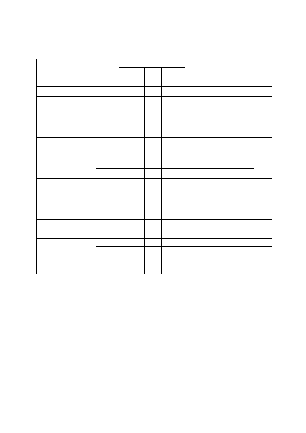
8-2 AC Characteristics (VDD = 4.5V ~ 5.5V , Ta = -20 ~ +70°C)
8-2-1 Write mode (writing data from MPU to DEM 16101-Series)
Characteristic Symbol Min Type Max Unit Test PIN
E Cycle Time t
C
500 --- --- ns E
E Rise Time
E Fall Time t
E Pulse width (High,Low)
R/W and RS Set-up Time t
R/W and RS Hold Time t
Data Set-up Time t
Data Hold Time t
t
R
F
t
W
SU1
H1
SU2
H2
--- --- 20 ns E
--- --- 20 ns E
230 --- --- ns E
40 --- --- ns R/W,RS
10 --- --- ns R/W,RS
80 --- --- ns DB0~DB7
10 --- --- ns DB0~DB7
Version:5 7
DEM 16101 SYH Product Specification
8-2-2 Read mode (reading data from DEM 16101-Series to MPU)
Characteristic Symbol Min Type Max Unit Test PIN
E Cycle Time t
C
500 --- --- ns E
E Rise Time
E Fall Time t
E Pulse width (High, Low)
R/W and RS Set-up Time t
R/W and RS Hold Time t
Data Output Delay Time t
Data Hold Time t
t
R
F
t
W
SU
H
D
DH2
--- --- 20 ns E
--- --- 20 ns E
230 --- --- ns E
40 --- --- ns R/W,RS
10 --- --- ns R/W,RS
--- ---
120
ns DB0~DB7
5 --- --- ns DB0~DB7
Version:5 8

DEM 16101 SYH Product Specification
9. CONTROL AND DISPLAY COMMAND
Command
clear L L L L L L L L L H 1.53ms Write “20H” to DDRAM and set
Display
Return home
Entry mode L L L L L L L H I/D SH 39us I/D:set cursor move direction
set H Increase
Display L L L L L L H D C B 39us Display
on/off H Display on
control
RS R/W DB7 DB6 DB5 DB4 DB3 DB2 DB1 DB0
L L L L L L L L H --- 1.53ms Cursor move to first digit
Execution time
(fosc=270KHz)
Remark
DDRAM address to “00H” from AC
I/D
SH:Specifies shift of display
SH H Display is shifted
D
Cursor
C
Blinking
B
l Decrease
L Display is not shifted
L Display off
H Cursor on
L Cursor off
H Blinking on
L Blinking off
Cursor L L L L L H S/C R/L --- --- 39us H Display shift
or
Display Shift
function L L L L H DL N F --- --- 39us H 8bits interface
Set
Set CGRAM L L L H AC5 AC4 AC3 AC2 AC1 AC0 39us CGRAM data is sent and
address received after this setting
Set DDRAM L L H AC6 AC5 AC4 AC3 AC2 AC1 AC0 39us DDRAM data is sent and
address received after this setting
Read busy L H BF AC6 AC5 AC4 AC3 AC2 AC1 AC0 0us
flag& H Busy
address
Write data H L D7 D6 D5 D4 D3 D2 D1 D0 43us Write data into DDRAM or
to RAM CGRAM
Read data H H D7 D6 D5 D4 D3 D2 D1 D0 43us Read data from DDRAM or
from RAM CGRAM
SC
R/L
DL
BF
-Reads BF indication
internal operating is being
performed
-Reads address counter
contents
L Cursor move
H Right shift
L Left shift
L 4bits interface
H 2 line display
N
L 1 line display
H Display on
F
L Display off
L Ready
Version:5 9
DEM 16101 SYH Product Specification
10. STANDARD CHARACTER PATTERN
Upper(4bit)
Lowerr(4bit)
LLLL
LLLL
CG RAM
(1)
LLLH LLHL LLHH LHLL LHLH LHHL LHHH HLLL HLLH HLHL HLHH HHLL HHLH HHHL HHHH
LLLH
LLHL
LLHH
LHLL
LHLH
LHHL
LHHH
HLLL
(2)
(3)
(4)
(5)
(6)
(7)
(8)
(1)
HLLH
HLHL
HLHH
HHLL
HHLH
HHHL
HHHH
(2)
(3)
(4)
(5)
(6)
(7)
(8)
Version:5 10
DEM 16101 SYH Product Specification
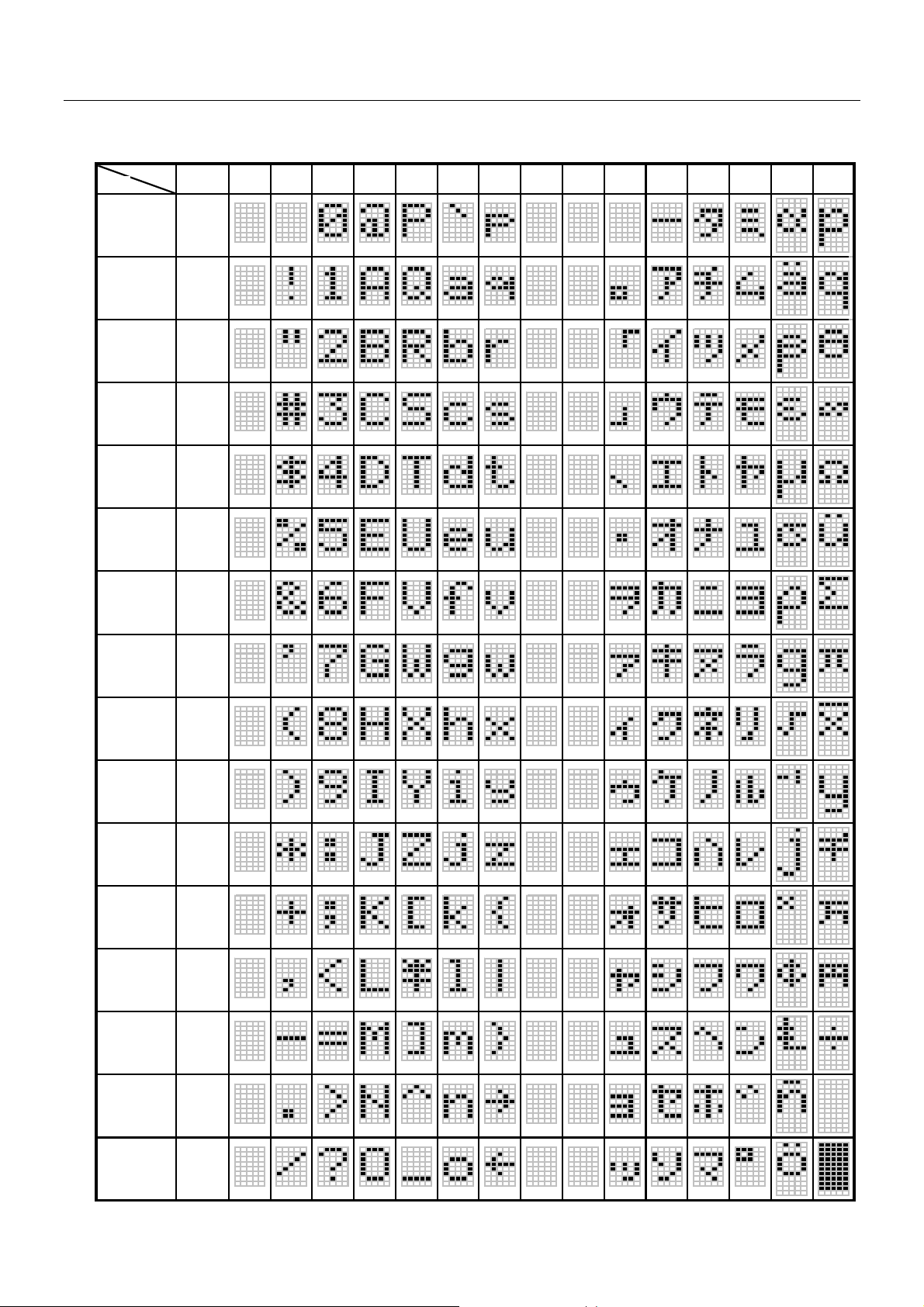
11. LCM INITIALIZING BY INSTRUCTION
11-1 8-bit interface mode
Power on
Wait for more than 30ms Condition : fosc=270khz
after VDD rises to 4.5v
Function set
RS RW DB7 DB6 DB5 DB4 DB3 DB2 DB1 DB0
0 0 0 0 1 1 N F X X 0 display off
Wait for more than 39us
Display on/off control
RS RW DB7 DB6 DB5 DB4 DB3 DB2 DB1 DB0
0 0 0 0 0 0 1 D C B 0 cursor off
Wait for more than 39us 0 blink off
Display clear
RS RW DB7 DB6 DB5 DB4 DB3 DB2 DB1 DB0
0 0 0 0 0 0 0 0 0 1
N
F
D
C
B
0 1-line mode
1 2-line mode
1 display on
0 display off
1 display on
1 cursor on
1 blink on
Wait for more than 1.53ms
Entry mode set
RS RW DB7 DB6 DB5 DB4 DB3 DB2 DB1 DB0
0 0 0 0 0 0 0 1 I/D SH
Initialization end
Version:5 11
I/D
SH
0 decrement mode
1 increment mode
0 entire shift off
1 entire shift on

DEM 16101 SYH Product Specification
11-2 4-bit interface mode
Power on
Wait for more than 30ms
after VDD rises to 4.5v
Function set
RS RW DB7 DB6 DB5 DB4 DB3 DB2 DB1 DB0 0 1-line mode
0 0 0 0 1 0 X X X X
0 0 0 0 1 0 X X X X 0 display off
0 0 N F X X X F X X
Wait for more than 39us
Display on/off control 0 display off
RS RW DB7 DB6 DB5 DB4 DB3 DB2 DB1 DB0
0 0 0 0 0 0 X X X X C 0 cursor off
0 0 1 D C B X X X X 1 cursor on
Wait for more than 39us
Condition : fosc=270khz
N
F
D
B
1 2-line mode
1 display on
1 Display on
0 blink off
1 blink on
Display clear
RS RW DB7 DB6 DB5 DB4 DB3 DB2 DB1 DB0
0 0 0 0 0 0 X X X X
0 0 0 0 0 1 X X X X
Wait for more than 1.53ms
Entry mode set 0 decrement mode
RS RW DB7 DB6 DB5 DB4 DB3 DB2 DB1 DB0
0 0 0 0 0 0 X X X X 0 entire shift off
0 0 0 1 I/D SH X X X X
Initialization end
I/D
SH
1 increment mode
1 entire shift on
Version:5 12

DEM 16101 SYH Product Specification
12. LCD Modules Handling Precautions
n The display panel is made of glass. Do not subject it to a mechanical shock by dropping it from a
high place, etc.
n If the display panel is damaged and the liquid crystal substance inside it leaks out, do not get any
in your mouth. If the substance come into contact with your skin or clothes promptly wash it off
using soap and water.
n Do not apply excessive force to the display surface or the adjoining areas since this may cause the
color tone to vary.
n The polarizer covering the display surface of the LCD module is soft and easily scratched. Handle
this polarize carefully.
n To prevent destruction of the elements by static electricity, be careful to maintain an optimum
work environment.
-Be sure to ground the body when handling the LCD module.
-Tools required for assembly, such as soldering irons, must be properly grounded.
-To reduce the amount of static electricity generated, do not conduct assembly and other work
under dry conditions.
-The LCD module is coated with a film to protect the display surface. Exercise care when peeling
off this protective film since static electricity may be generated.
n Storage precautions
When storing the LCD modules, avoid exposure to direct sunlight or to the light of fluorescent
lamps. Keep the modules in bags designed to prevent static electricity charging under low
temperature / normal humidity conditions (avoid high temperature / high humidity and low
temperatures below 0°C).Whenever possible, the LCD modules should be stored in the same
conditions in which they were shipped from our company.
13. Others
n Liquid crystals solidify at low temperature (below the storage temperature range) leading to
defective orientation of liquid crystal or the generation of air bubbles (black or white). Air bubbles
may also be generated if the module is subjected to a strong shock at a low temperature.
n If the LCD modules have been operating for a long time showing the same display patterns may
remain on the screen as ghost images and a slight contrast irregularity may also appear. Abnormal
operating status can be resumed to be normal condition by suspending use for some time. It should
be noted that this phenomena does not adversely affect performance reliability.
n To minimize the performance degradation of the LCD modules resulting from caused by static
electricity, etc. exercise care to avoid holding the following sections when handling the modules:
- Exposed area of the printed circuit board
- Terminal electrode sections
Version:5 13
 Loading...