Diodes ZDT6790 User Manual

A
f
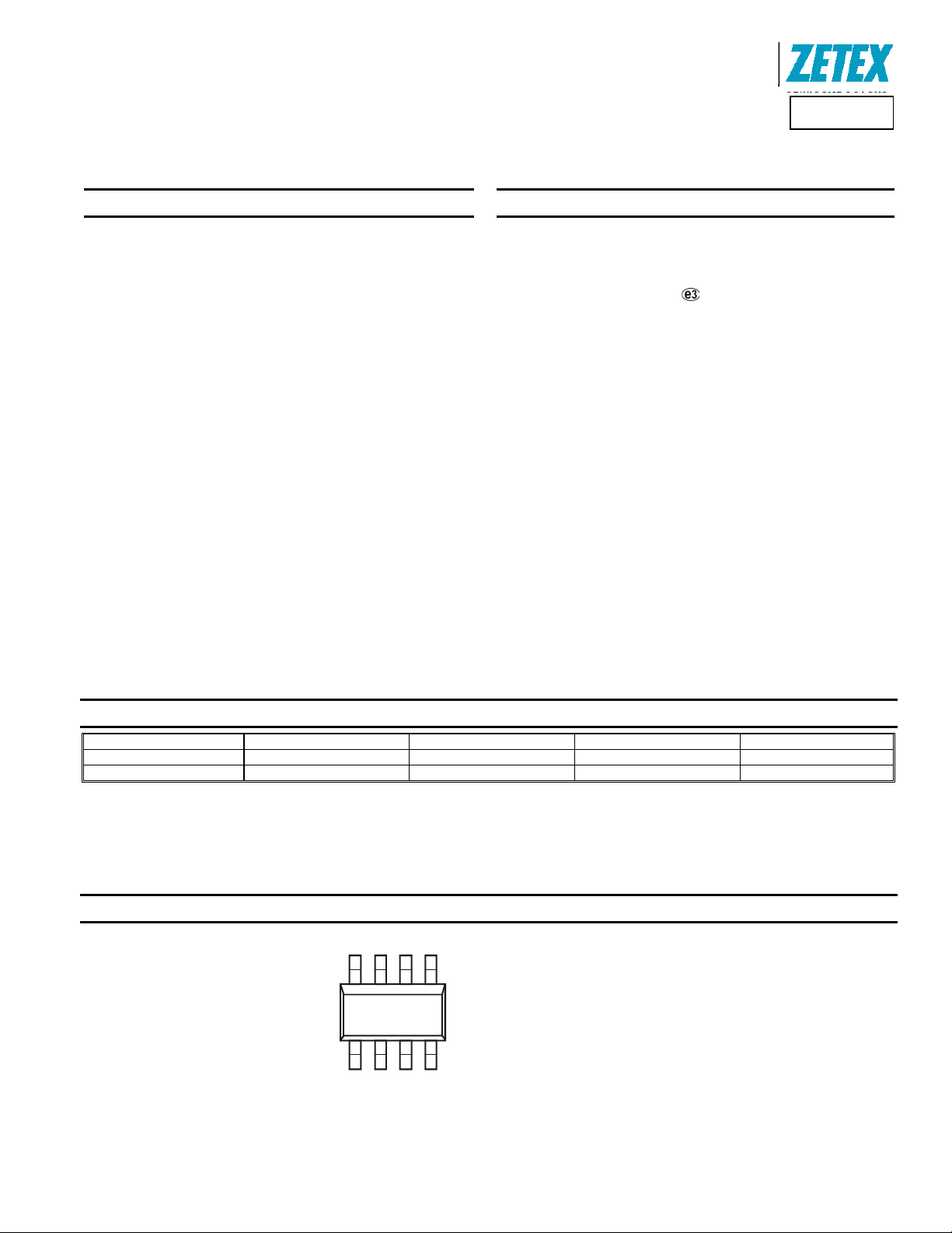
COMPLEMENTARY MEDIUM POWER HIGH GAIN TRANSISTOR IN SM-8 PACKAGE
Features
• NPN Transistor
BV
V
Continuous Current I
• PNP Transistor
BV
V
Continuous Current I
• Lead-Free Finish; RoHS Compliant (Notes 1 & 2)
• Halogen and Antimony Free. “Green” Device (Note 3)
• Qualified to AEC-Q101 Standards for High Reliability
> 45
CEO
< 100mV @ IC= 100mA
CE(sat)
> -40V
CEO
< 250mV @ IC= -500mA
CE(sat)
= 2A
C
= -2A
C
SM-8
Top View
Green
Top View
Pin Out
Product Line o
Diodes Incorporated
ZDT6790
Mechanical Data
• Case: SM-8 (8 LEAD SOT223)
• Case Material: Molded Plastic, “Green” Molding Compound. UL
Flammability Classification Rating 94V-0
• Moisture Sensitivity: Level 1 per J-STD-020
• Terminals: Matte Tin Finish
• Weight: 0.117 grams (approximate)
Equivalent Circuit
Ordering Information (Note 4)
Part Number Marking Reel size (inches) Tape width (mm) Quantity per reel
ZDT6790TA T6790 7 12 1,000
ZDT6790TC T6790 13 12 4,000
Notes: 1. EU Directive 2002/95/EC (RoHS) & 2011/65/EU (RoHS 2) compliant. All applicable RoHS exemptions applied.
2. See http://www.diodes.com for more information about Diodes Incorporated’s definitions of Halogen- and Antimony-free, "Green" and Lead-free.
3. Halogen- and Antimony-free "Green” products are defined as those which contain <900ppm bromine, <900ppm chlorine (<1500ppm total Br + Cl) and
<1000ppm antimony compounds.
4. For packaging details, go to our website at http://www.diodes.com
Marking Information
T6790
T6790 = Product Type Marking Code
ZDT6790
Document number: DS33210 Rev. 2 - 2
1 of 9
www.diodes.com
July 2012
© Diodes Incorporated

A
f
Product Line o
Diodes Incorporated
Maximum Ratings (@T
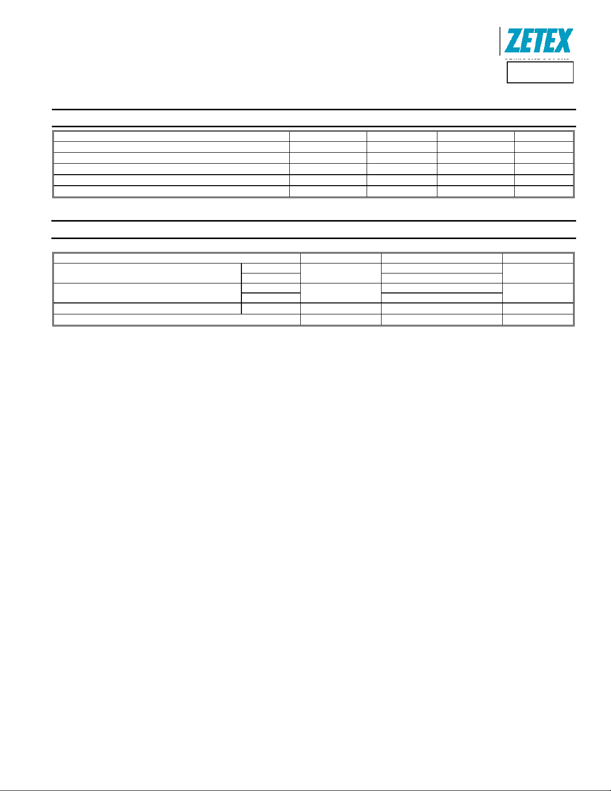
Characteristic Symbol NPN PNP Unit
Collector-Base Voltage
Collector-Emitter Voltage
Emitter-Base Voltage
Continuous Collector Current
Peak Pulse Current (Note 5)
Thermal Characteristics (@T
Collector Power Dissipation
Thermal Resistance, Junction to Ambient
Thermal Resistance, Junction to Leads (Note 7)
Operating and Storage Temperature Range
Notes: 5. For the device with any single die active, mounted on 25mm x 25mm FR4 PCB with high coverage of single sided 2oz copper, in still air conditions .
6. For the device with both die active, mounted on 25mm x 25mm FR4 PCB with high coverage of single sided 2oz copper, in still air conditions.
7. Thermal resistance from junction to solder-point (at the end of the collector lead).
= +25°C, unless otherwise specified.)
A
V
CBO
V
CEO
V
EBO
I
C
I
CM
= +25°C, unless otherwise specified.)
A
Characteristic Symbol Value Unit
(Note 5)
(Note 6) 2.75
(Note 5)
(Note 6) 45.50
R
R
T
J,TSTG
P
θJA
θJL
D
45
45
6
2
6
2.25
55.60
30.68
-55 to +150
-50 V
-40 V
-6 V
-2 A
-6 A
ZDT6790
W
°C/W
°C/W
°C
ZDT6790
Document number: DS33210 Rev. 2 - 2
2 of 9
www.diodes.com
July 2012
© Diodes Incorporated

A
f
Product Line o
Diodes Incorporated
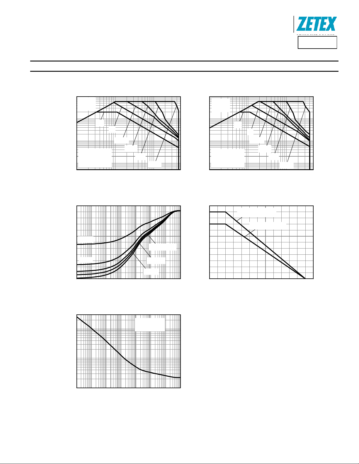
Thermal Characteristics
10
R
CE(SAT)
Limited
1
100m
10m
Collector Current (A)
C
I
0.1 1 10
DC
One active die
Single Pulse
T
=25°C
amb
1s
VCE Collecto r- Emi tte r Voltage (V)
NPN Safe Operating Area
50
40
D=0.5
30
20
D=0.2
10
Thermal Resistance (°C/W)
0
100µ 1m 10m 100m 1 10 100 1k
Puls e Width ( s)
100ms
10ms
1ms
100us
Single Pulse
D=0.05
D=0.1
10
R
CE(SAT)
Limited
1
DC
1s
100m
One active die
Single Pulse
10m
Collector Current (A)
T
=25°C
amb
C
-I
0.1 1 10
100ms
10ms
1ms
100us
-VCE Colle cto r- Emitter Volta g e (V)
PNP Safe Operating Area
3.0
2.5
2.0
1.5
1.0
0.5
0.0
0 25 50 75 100 125 150
Max Power Dissipation (W)
Two active die
One active die
Temperature (°C)
ZDT6790
Transient Thermal Impedance
Single Pulse
=25°C
100
10
T
amb
Dera ting C urv e
Maximum Power (W)
1
100µ 1m 10m 100m 1 10 100 1k
Puls e Width ( s)
Pulse Power Dissipation
ZDT6790
Document number: DS33210 Rev. 2 - 2
3 of 9
www.diodes.com
© Diodes Incorporated
July 2012
 Loading...