Diodes US1A, US1B, US1D, US1G, US1J Schematic [ru]
...
Features
Glass Passivated Die Construction
Ultra-Fast Recovery Time for High Efficiency
Surge Overload Rating to 30A Peak
High Current Capability
Ideally Suited for Automated Assembly
Lead-Free Finish; RoHS Compliant (Note 1)
Halogen and Antimony Free. “Green” Device (Note 2)
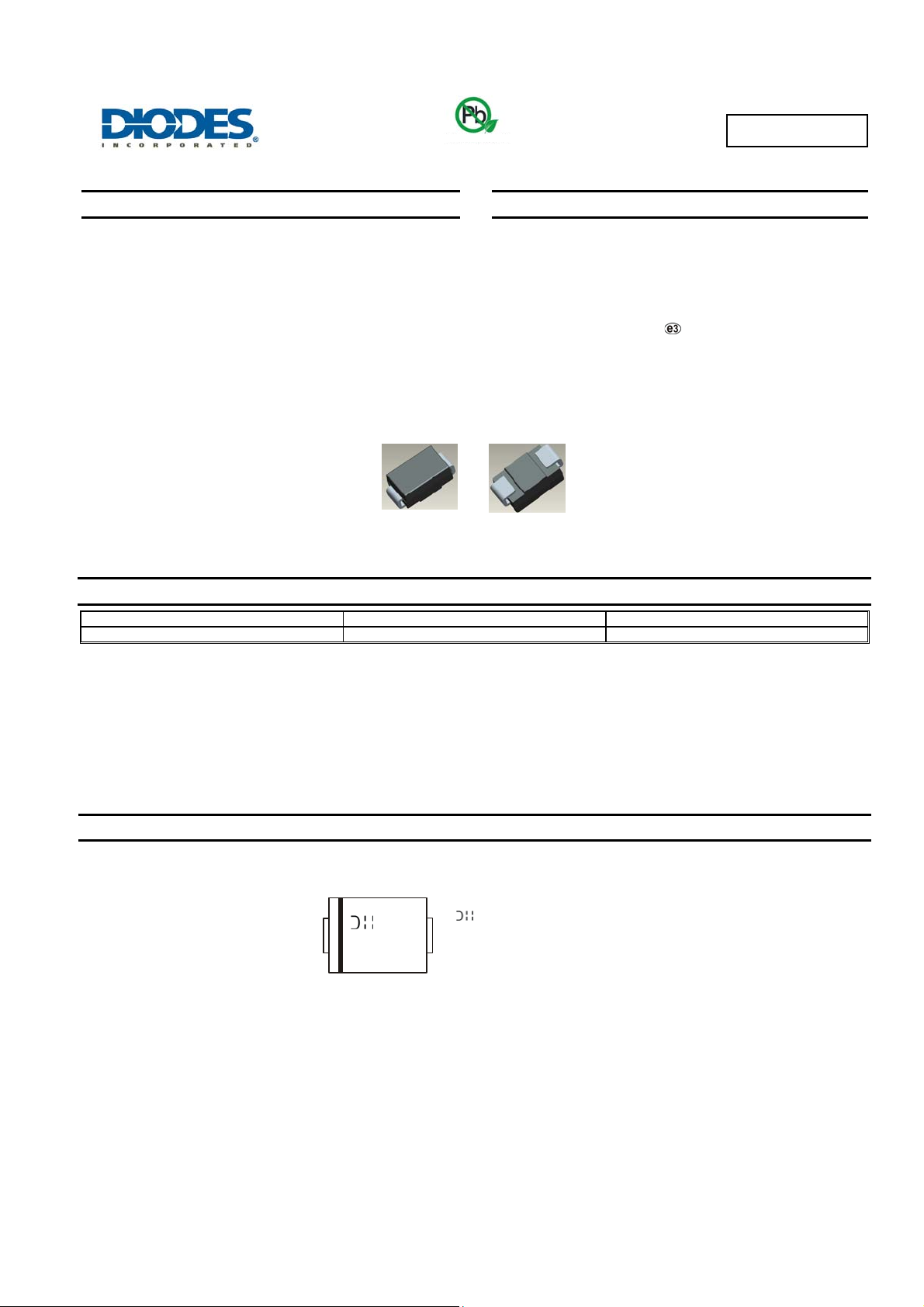
Top View
Green
US1A - US1M
1.0A SURFACE MOUNT ULTRA-FAST RECTIFIER
Mechanical Data
Case: SMA
Case Material: Molded Plastic. UL Flammability Classification
Rating 94V-0
Moisture Sensitivity: Level 1 per J-STD-020
Terminals: Lead Free Plating (Matte Tin Finish). Solderable per
MIL-STD-202, Method 208
Polarity: Cathode Band or Cathode Notch
Weight: 0.064 grams (Approximate)
Bottom View
Ordering Information (Note 3)
Part Number* Case Packaging
US1x-13-F SMA 5,000/Tape & Reel
*x = Device type, e.g. US1A-13-F.
Notes: 1. EU Directive 2002/95/EC (RoHS) & 2011/65/EU (RoHS 2) compliant. All applicable RoHS exemptions applied.
2. See http://www.diodes.com/quality/lead_free.htm l for more information about Diodes Incorporated’s definitions of Halogen- and Antimony-free, "Green"
and Lead-free.
3. Halogen- and Antimony-free "Green” products are defined as those which contain <900ppm bromine, <900ppm chlorine (<1500ppm total Br + Cl) and
<1000ppm antimony compounds.
Marking Information
US1A - US1M
Document number: DS16008 Rev. 11 - 2
YWW
US1x
US1x = Product Type Marking Code, ex: US1A
= Manufacturers’ Code Marking
YWW = Date Code Marking
Y = Last Digit of Year (ex: 4 for 2014)
WW = Week Code (01 to 53)
1 of 5
www.diodes.com
December 2014
© Diodes Incorporated

)
E
RAGE REC
T
ED C
URR
E
N
T
NSTAN
TAN
EOU
S
RWAR
C
U
R
REN
T
Maximum Ratings (@T
= +25°C unless otherwise specified.)
A
Single phase, half wave, 60Hz, resistive or inductive load.
For capacitance load, derate current by 20%.
Characteristic Symbol US1A US1B US1D US1G US1J US1K US1M Unit
Peak Repetitive Reverse Voltage
Working Peak Reverse Voltage
DC Blocking Voltage (Note 4)
RMS Reverse Voltage
V
V
V
R(RMS
RRM
RWM
V
Average Rectified Output Current @ TT = +75°C IO
Non-Repetitive Peak Forward Surge Current 8.3ms
Single Half Sine-Wave Superimposed on Rated Load
I
FSM
Thermal Characteristics
Characteristic Symbol Value Unit
Maximum Thermal Resistance, Junction to Terminal
Operating and Storage Temperature Range
Electrical Characteristics (@T
= +25°C unless otherwise specified.)
A
Characteristic Symbol US1A US1B US1D US1G US1J US1K US1M Unit
Forward Voltage Drop @ IF = 1.0A VFM
Peak Reverse Current @ TA = +25°C
at Rated DC Blocking Voltage (Note 4) @ T
= +100°C
A
Reverse Recovery Time (Note 5)
Typical Total Capacitance (Note 6)
Notes: 4. Short duration pulse test used to minimize self-heating effect.
5. Measured with IF = 0.5A, IR = 1.0A, Irr = 0.25A. See Figure 5.
6. Measured at 1.0MHz and applied reverse voltage of 4.0V DC.
(A)
1.0
R
T
J, TSTG
I
RM
t
C
US1A - US1M
50 100 200 400 600 800 1000 V
R
35 70 140 280 420 560 700 V
1.0 A
JT
1.0 1.3 1.7 V
rr
T
50 75 ns
20 10 pF
10
(A)
D
1.0
30 A
30 °C/W
-65 to +150 °C
5.0
100
US1A - US1D
US1G
µA
IFI
FO
US1J - US1M
0.5
0.1
O
I, AV
0
25 50
T , TERMINAL TEMPERATURE ( C)
75
T
100 125 150
°
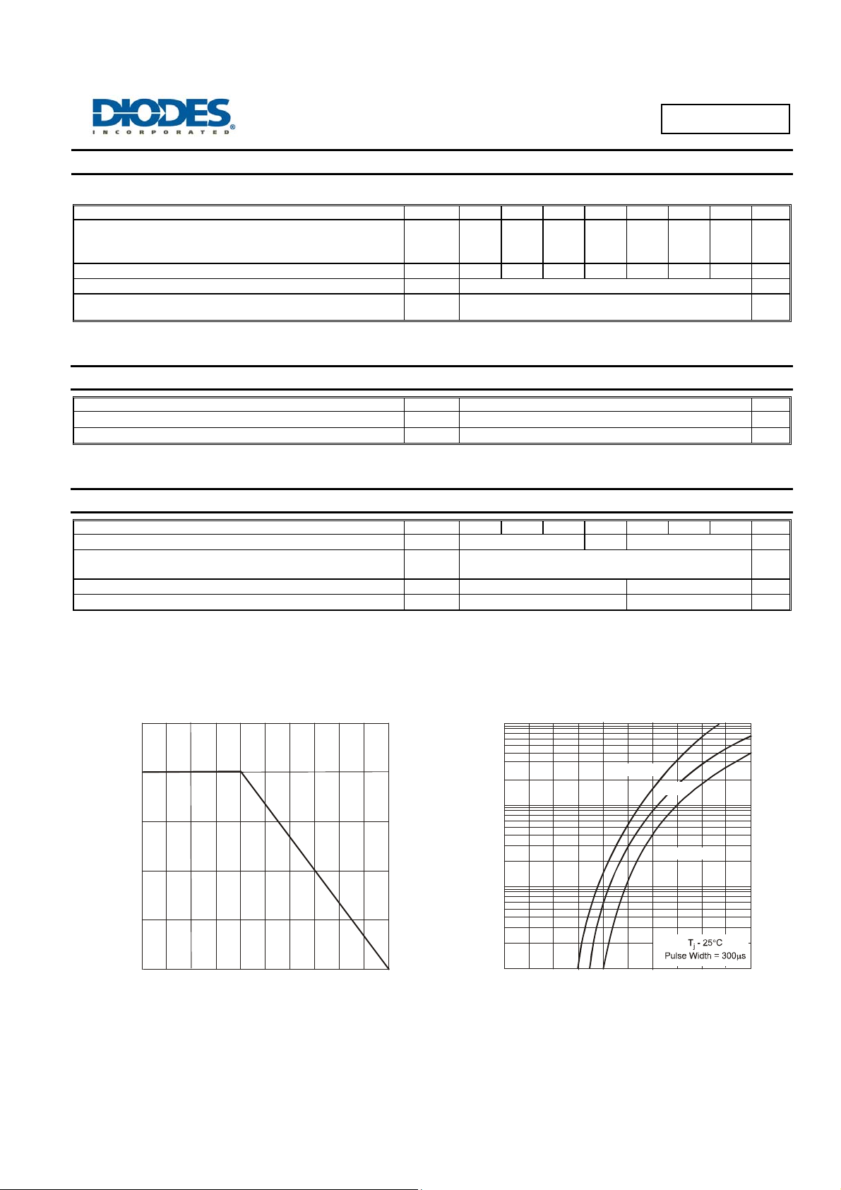
Fig. 1 Forward Current Derating Curve
F
0.01
I, I
00.40.8
V , INST ANTANEOUS FORWARD VOLTAG E (V)
F
Fig. 2 Typical Forward Characteristics
1.2 1.6 2.0
US1A - US1M
Document number: DS16008 Rev. 11 - 2
2 of 5
www.diodes.com
December 2014
© Diodes Incorporated
 Loading...