Diodes SBR05M100BLP User Manual

)
θ
θ
(BR)
g
Features
• Ultra Low Leakage Current
• Excellent High Temperature Stability
• Patented Super Barrier Rectifier Technology
• Soft, Fast Switching Capability
• 150ºC Operating Junction Temperature
• Lead Free Finish, RoHS Compliant (Note 1)
• “Green” Device (Note 4)
1
2
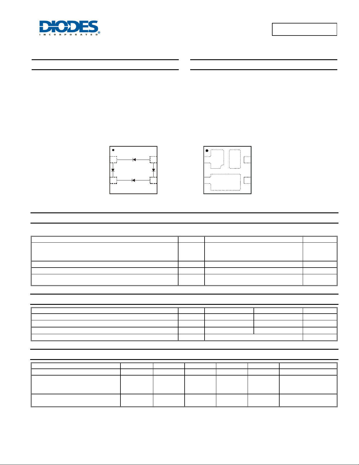
Top View
Device Schematic
SBR05M100BLP
®
0.5A SBR
BRIDGE
SUPER BARRIER RECTIFIER
Mechanical Data
• Case: DFN3030-4
• Case Material: Molded Plastic “Green” Molding Compound,
UL Flammability Classification Rating 94V-0
• Moisture Sensitivity: Level 1 per J-STD-020
• Terminals: Finish – NiPdAu Over Copper Lead Frame,
Solderable per MIL-STD-202, Method 208
• Polarity: See Diagram
• Marking Information: See Page 3
• Ordering Information: See Page 3
• Weight: 0.02 grams (approximate)
4
3
1
~
+
2
N/C
-
4
3
~
Top View
Pin Confi
uration
Maximum Ratings @T
= 25°C unless otherwise specified
A
Single phase, half wave, 60Hz, resistive or inductive load.
For capacitance load, derate current by 20%.
Characteristic Symbol Value Unit
V
Peak Repetitive Reverse Voltage
Working Peak Reverse Voltage
DC Blocking Voltage
RMS Reverse Voltage
Average Rectified Output Current
Non-Repetitive Peak Forward Surge Current 8.3ms
Single Half Sine-Wave Superimposed on Rated Load (Per Diode)
V
V
R(RMS
RRM
RWM
V
I
FSM
RM
I
O
100 V
70 V
500 mA
8 A
Thermal Characteristics
Characteristic Symbol Typ Max Unit
Power Dissipation (Note 2)
Thermal Resistance Junction to Ambient Air (Note 2)
Thermal Resistance Junction to Ambient Air (Note 3)
Operating and Storage Temperature Range
P
D
R
JA
R
JA
, T
T
J
STG
Electrical Characteristics @T
= 25°C unless otherwise specified
A
Characteristic Symbol Min Typ Max Unit Test Condition
Reverse Breakdown Voltage (Note 4)
V
R
100 - - V
0.54
Forward Voltage (Per Diode)
Reverse Current (Note 4) (Per Diode)
Notes: 1. EU Directive 2002/95/EC (RoHS). All applicable RoHS exemptions applied, see EU Directive 2002/95/EC Annex Notes.
SBR is a registered trademark of Diodes Incorporated.
2. FR-4 PCB, 2 oz. Copper, minimum recommended pad layout per http://www.diodes.com/datasheets/ap02001.pdf.
3. Polymide PCB, 2 oz. copper; minimum recommended pad layout per http://www.diodes.com/datasheets/ap02001.pdf.
4. Diodes Inc.’s “Green” policy can be found on our website at http://www.diodes.com/products/lead_free/index.php
5. Short duration pulse test used to minimize self-heating effect.
V
F
I
R
SBR05M100BLP
Document number: DS31109 Rev. 8 - 2
-
-
www.diodes.com
0.67
0.56
0.3
32
1 of 4
- 0.56 W
- 222 °C/W
- 149 °C/W
-55 to +150 °C
IR = 250 μA
I
0.60
0.73
0.63
25
250
V
µA
= 0.25A, TJ = 25ºC
F
= 0.5A, TJ = 25ºC
I
F
I
= 0.5A, TJ = 125ºC
F
= 100V, TJ = 25ºC
V
R
= 100V, TJ = 125ºC
V
R
June 2010
© Diodes Incorporated

P
P
O
R
PAT
O
S
ANTA
OUS FO
R
A
R
CUR
R
m
A
TANT
O
US R
R
CUR
RENT
RAG
O
RWARD CUR
REN
T
T
RAT
N
T
T
P
RATUR
C
SBR05M100BLP
0.9
1,000
)
0.8
0.7
N (W)
0.6
I
0.5
DISSI
0.4
WE
0.3
,
D
0.2
D
W
NE
T
100
10
1
0.1
T = 125°C
A
T = 85°C
A
T = 25°C
A
ENT (
0.1
F
-I , IN
0
0 0.5 1 1.5
I , AVERAGE FORWARD CURRENT (A)
F(AV)
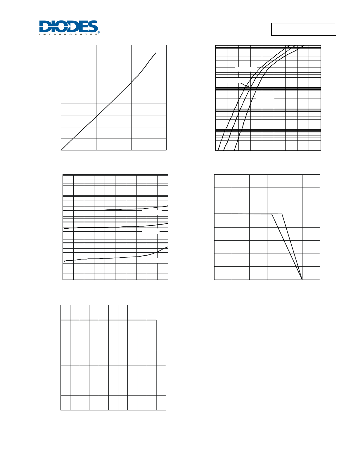
Fig. 1 Forward Power Dissipation
1,000
(µA)
0.01
0 100 200 300 400 500 600 700 800 900
-V , INSTANTANE OUS FORWARD VO LTAGE (m V)
F
Fig. 2 Typical Forward Characteristics
0.8
(A)
0.7
100
0.6
SE
10
EVE
1
ANE
0.1
R
0.01
-I , INS
0102030405060708090100
-V , INSTANTANEOUS REVERSE VOLTAGE (V)
R
Fig. 3 Typical Reverse Characteristics
175
)
150
E (°
125
E
EM
100
75
50
ED AMBIE
T = 125°C
A
T = 85°C
A
T = 25°C
A
0.5
Note 3
Per Diode
0.4
E F
0.3
Note 2
Per Diode
0.2
0.1
F(AV)
I, AVE
0
25 50 75 100 125 150 175
T , AMBIENT TEMPERATURE (°C)
A
Fig. 4 Forward Current Derating Curve
25
, DE
A
0
0102030405060708090100
V , DC REVERSE VOLTAGE (V)
R
110
Fig. 5 Operating Temperature Derating
SBR is a registered trademark of Diodes Incorporated.
SBR05M100BLP
Document number: DS31109 Rev. 8 - 2
2 of 4
www.diodes.com
June 2010
© Diodes Incorporated
 Loading...