Diodes MBRF20200CT User Manual

g
A
A
MBR20200CT / MBRF20200CT
Green
20A SCHOTTKY BARRIER RECTIFIER
Product Summary
MBR20200CT / MBRF20200CT (Per Leg)
V
(V)
(V) IO (A)
V
RRM
200 10 0.89 0.1
F (MAX)
@ +25°C
IR
(MAX)
@ +25°C
(mA)
Description and Applications
This Schottky Barrier Rectifier has been designed to meet the
general requirements of commercial applications. It is ideally suited for
use as:
Polarity Protection Diode
Re-Circulating Diode
Switching Diode
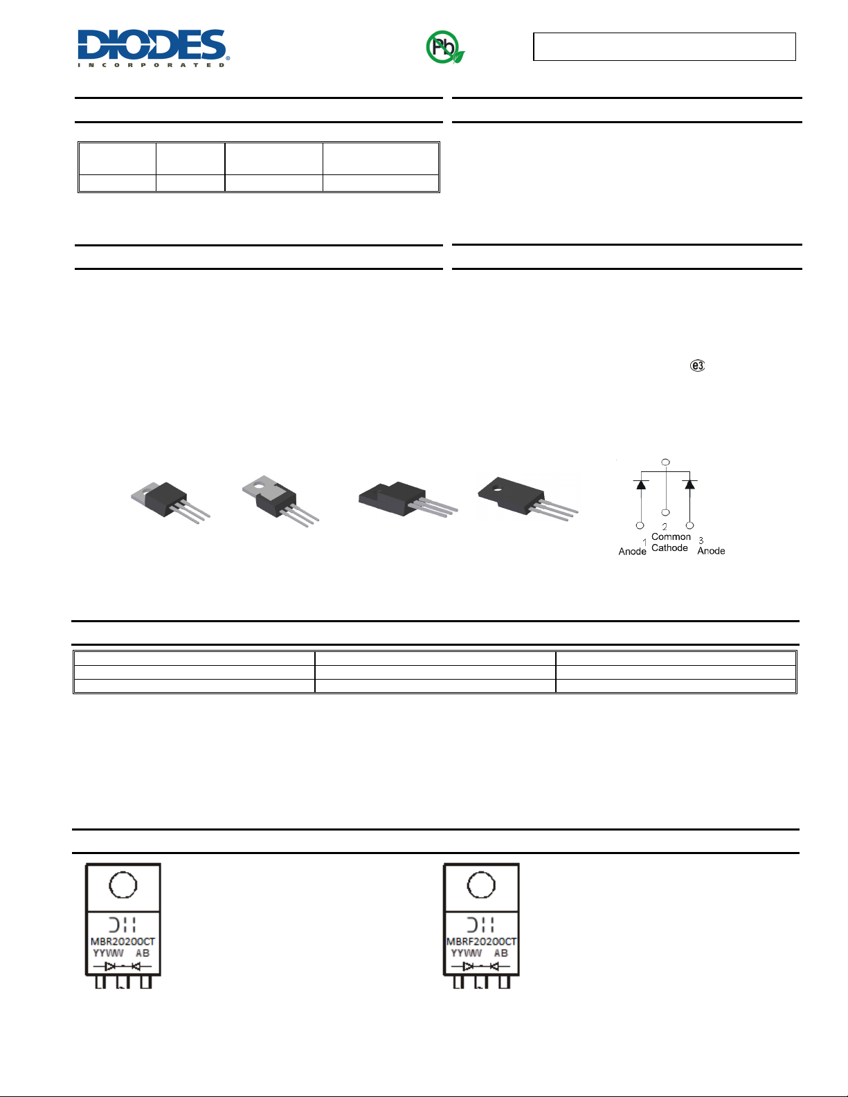
TO-220AB
Top View
TO-220AB
Bottom View
ITO-220AB
Top View
Features and Benefits
Guard Ring Die Construction for Transient Protection.
High Surge Current Capability.
Low Forward Voltage Drop.
Lead-Free Finish; RoHS Compliant (Notes 1 & 2)
Halogen and Antimony Free. “Green” Device (Note 3)
Qualified to AEC-Q101 Standards for High Reliability
Mechanical Data
Case: TO-220AB, ITO-220AB
Case Material: Molded Plastic, “Green” Molding compound. UL
Flammability Classification Rating 94V-0
Moisture Sensitivity: Level 1 per J-STD-020
Terminals: Finish - Matte Tin annealed over Copper leadframe.
Solderable per MIL-STD-202, Method 208
Polarity: See Below
Weight: TO-220AB – 1.95 grams (approximate)
ITO-220AB – 1.69 grams (approximate)
ITO-220AB
Bottom View
Package Pin Out
uration
Confi
Ordering Information
Part Number Case Packaging
MBR20200CT-LJ TO-220AB (Type C) 50 pieces/tube
MBRF20200CT-LJ ITO-220AB (TO220F-3) 50 pieces/tube
Notes: 1. EU Directive 2002/95/EC (RoHS) & 2011/65/EU (RoHS 2) compliant. All applicable RoHS exemptions applied.
2. See http://www.diodes.com/quality/lead_free.html for more information about Diodes Incorporated’s definitions of Halogen- and Antimony-free, "Green"
and Lead-free.
3. Halogen- and Antimony-free "Green” products are defined as those which contain <900ppm bromine, <900ppm chlorine (<1500ppm total Br + Cl) and
<1000ppm antimony compounds.
4. For packaging details, go to our website at http://www.diodes.com/products/packages.html.
(Notes 4)
Marking Information
MBR20200CT = Product Type Marking Code
B = Foundry and Assembly Code
YYWW = Date Code Marking
YY = Last two digits of year (ex: 13 = 2013)
WW = Week (01 - 53)
MBRF20200CT = Product Type Marking Code
B = Foundry and Assembly Code
YYWW = Date Code Marking
YY = Last two digits of year (ex: 13 = 2013)
WW = Week (01 - 53)
MBR20200CT / MBRF20200CT
Document number: DS36513 Rev. 5 - 2
1 of 4
www.diodes.com
December 2013
© Diodes Incorporated

P, P
OWER
P
T
O
Maximum Ratings (Per Leg) (@T
= +25°C, unless otherwise specified.)
A
Single phase, half wave, 60Hz, resistive or inductive load.
For capacitance load, derate current by 20%.
Characteristic Symbol Value Unit
Peak Repetitive Reverse Voltage
Working Peak Reverse Voltage
DC Blocking Voltage
Average Rectified Output Current (Per Leg)
(Total)
Non-Repetitive Peak Forward Surge Current 8.3ms
Single Half Sine-Wave Superimposed on Rated Load
Thermal Characteristics (Per Leg)
Characteristic Symbol Value Unit
Typical Thermal Resistance, Junction to Case (Note 5)
Package = TO-220AB
Package = ITO-220AB
Typical Thermal Resistance, Junction to Ambient (Note 5)
Package = TO-220AB
Package = ITO-220AB
Operating and Storage Temperature Range
MBR20200CT / MBRF20200CT
V
RRM
V
RWM
V
RM
I
O
I
FSM
R
θJC
R
θJA
T
, T
J
STG
200 V
10
20
A
170 A
3
°C/W
5
15
°C/W
25
-55 to +175 °C
Electrical Characteristics (Per Leg) (@T
= +25°C, unless otherwise specified.)
A
Characteristic Symbol Min Typ Max Unit Test Condition
Forward Voltage Drop
Leakage Current (Note 6)
Notes: 5. Device mounted on heat sink (45mm x 20mm x12mm), with minimum recommended pad layout per http://www.diodes.com
6. Short duration pulse test used to minimize self-heating effect
V
F
I
R
—
—
—
—
0.85
—
—
—
0.89
0.75
0.1
10
V
mA
8.0
T = 175°C
J
6.0
N (W)
I
A
4.0
DISSI
100
10
0.1
1
T = 150°C
T = 125°C
A
T = 175°C
A
A
T = 85°C
A
T = 25°C
A
0.01
2.0
D
0.001
I
= 10A, TJ = +25°C
F
I
= 10A, TJ = +125°C
F
V
= 200V, TJ = +25°C
R
= 200V, TJ = +125°C
V
R
F
0.0
024681012
I AVERAGE FORWARD CURRENT (A)
F(AV)
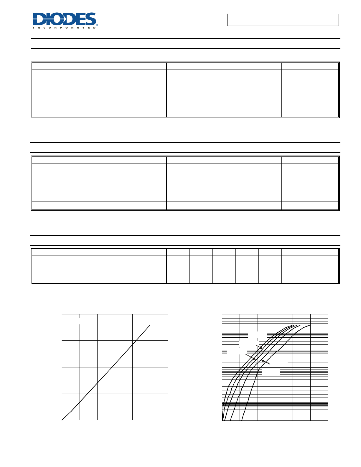
Figure 1 For ward Power Dissipation
MBR20200CT / MBRF20200CT
Document number: DS36513 Rev. 5 - 2
2 of 4
www.diodes.com
I , INSTANTANEOUS FORWARD CURRENT (A)
0.0001
0 0.2 0.4 0.6 0.8 1 1.2
V , INSTANTANEOUS FORWARD VOLTAGE (V)
F
Figure 2 Typical Forward Characteristics
December 2013
© Diodes Incorporated
 Loading...