

Page 1
(
)
9
AP78LXX SERIES 3-TERMINAL POSITIVE REGULATORS
Description
The AP78LXX Series is a three terminal positive regulator
available with fixed output voltages from 5V, 8V and 12V,
making them useful in a wide range of applications. When
used as a Zener diode/resistor combination replacement, the
AP78LXX can improve output impedance by two orders of
magnitude, and lower quiescent current. These regulators
can provide local on card regulation, eliminating the
distribution problems associated with single point regulation.
The voltages available allow the AP78LXX's to be used in
logic systems. Instrumentation, HiFi and other solid state
electronic equipment.
The AP78LXX is available in the plastic TO92, SOT89 and
SO-8 using industrial standard package technology. The
regulator can deliver 100mA output current with adequate
heat sinking. Current limiting is included to limit the peak
output current to a safe value. Safe area protection for the
output transistors is provided to limit internal power
dissipation. Thermal overload protection is integrated to
prevent the IC from overheat due to abnormal condition.
Features
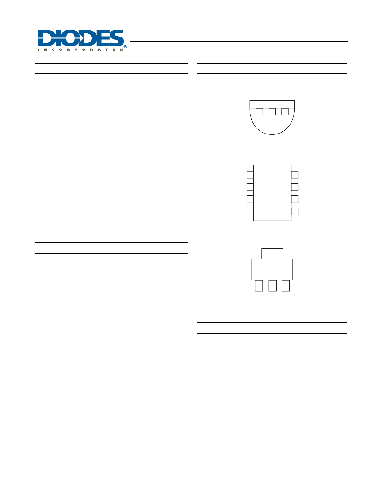
Pin Assignments
(Bottom View)
V
1
V
OUT
GND
2
3
GND
NC
4
AP78L05/08/12
V
GND
OUT
TO92
(To p V iew)
SO-8
Top View
IN
V
8
IN
GND
7
6
GND
NC
5
• Output voltages of 5.0V, 8.0V, 12V
• Output voltage tolerances of ±5% over the operating
temperature ranges
• Output current in excess of 100mA
• Internal thermal overload protection
• Output transistor safe area protection
• Internal short circuit current limiting
• No external components
• Available in plastic TO92, SOT89 and plastic SO-8 low
profile packages
• Lead Free Package: TO92 (Note 1)
• SO-8 and SOT89: Available in “Green” Molding
Compound (No Br, Sb) (Note 2)
• Lead Free Finish / RoHS Compliant (Note 3)
Applications
• Communication
• CD-ROM
• DVD-Player
• Set-Top Box
123
GND
V
V
OUT
SOT8
IN
Notes: 1. TO92 is available in “Lead Free” product only.
2. SO-8 and SOT89 are available in “Green” products only.
3. EU Directive 2002/95/EC (RoHS) & 2011/65/EU (RoHS 2). All applicable RoHS exemptions applied.
AP78L05/08/12
Document number: DS31054 Rev. 10 - 2
1 of 16
www.diodes.com
March 2012
© Diodes Incorporated
Page 2
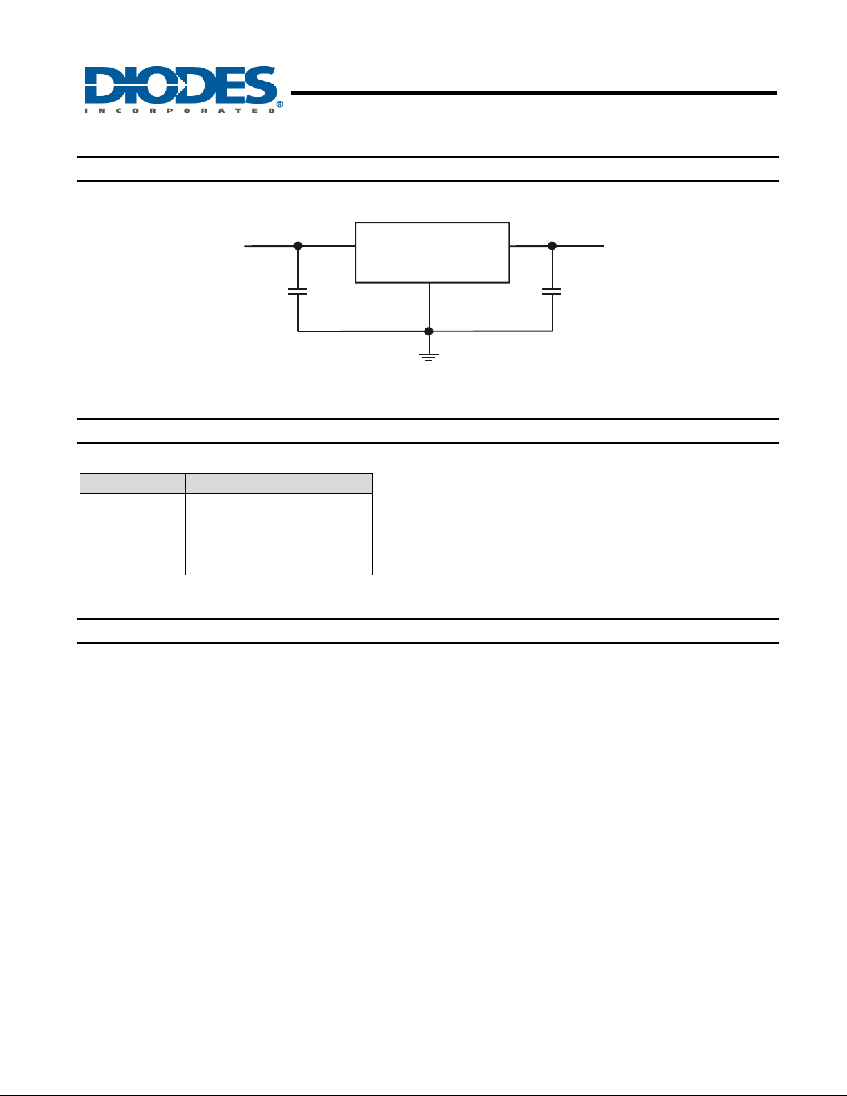
Typical Application Circuit
AP78L05/08/12
AP78LXX SERIES 3-TERMINAL POSITIVE REGULATORS
Fixed Output Regulator
Input Output
†
C1
AP78Lxx
GND
0.33µF
(†) Required if the regulator is located more than 3” from the power supply filter
(‡) See Note 5 in the electrical characteristics table
IN
OUT
‡
C2
0.1µF
Pin Descriptions
Pin Name Description
VIN
V
OUT
GND Ground
NC No Connection
Operating Voltage Input
Voltage Output Pin
Functional Block Diagram
Introduction
The AP78LXX series is a three terminal device with fixed output voltages from 5V,8V and 12V. T he AP78LXX fixed voltage
regulator series has built-in thermal overload protection which prevents the device from being damaged due to excessive
junction temperature. The regulator also contains internal short-circuit protection which limits the maximum output current, an d
safe-area protection for the pass transistor which reduces the short-circuit current as the voltage across the pass transistor is
increased.
AP78L05/08/12
Document number: DS31054 Rev. 10 - 2
2 of 16
www.diodes.com
March 2012
© Diodes Incorporated
Page 3
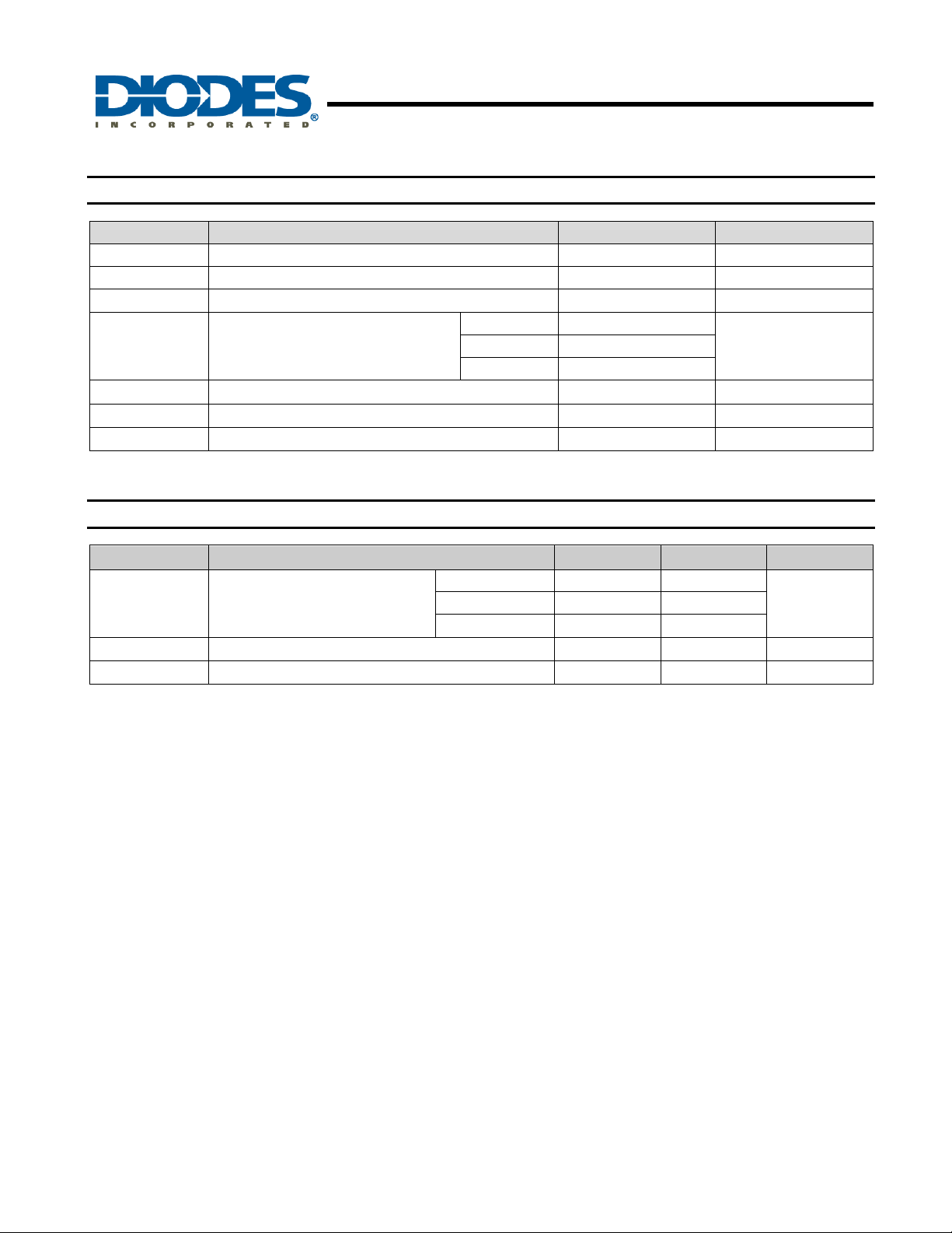
AP78L05/08/12
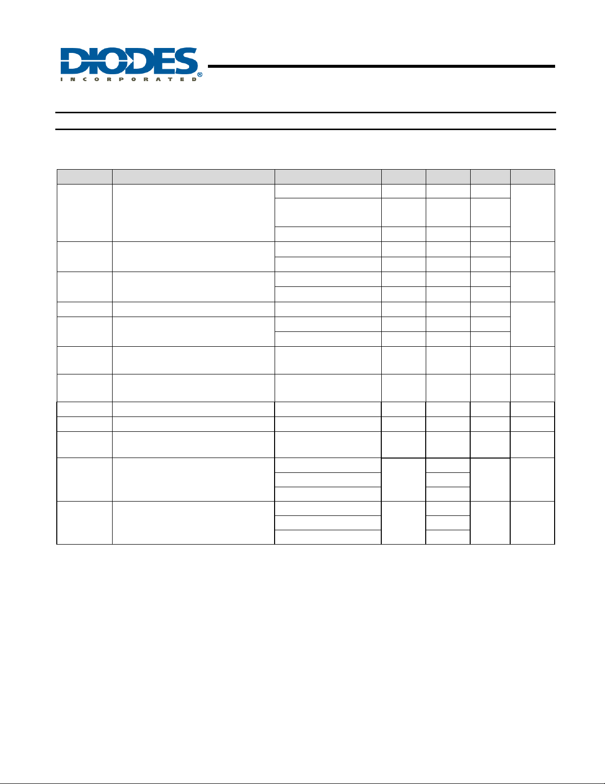
Absolute Maximum Ratings (T
Symbol Parameter Rating Unit
ESD HBM Human Body Model ESD Protection 3 KV
ESD MM Machine Model ESD Protection 250 V
VCC
V
OUT
TST
TOP
TMJ
Recommended Operating Conditions (T
Symbol Parameter Min Max Unit
VIN
I
OUT
TA
AP78L05/08/12
Document number: DS31054 Rev. 10 - 2
Supply Voltage
Output Voltage to Ground
Storage Temperature
Operating Junction Temperature
Maximum Junction Temperature
Input Voltage
Output Current 0 100 mA
Operating Ambient Temperature -20 +85
AP78LXX SERIES 3-TERMINAL POSITIVE REGULATORS
= 25°C)
A
30 V
AP78L05 5
AP78L08 8
AP78L12 12
-65 to +150 °C
-20 to +125 °C
150 °C
= 25°C)
A
AP78L05 7 20
AP78L08 10.5 23
AP78L12 14.5 27
3 of 16
www.diodes.com
V
V
o
C
March 2012
© Diodes Incorporated
Page 4
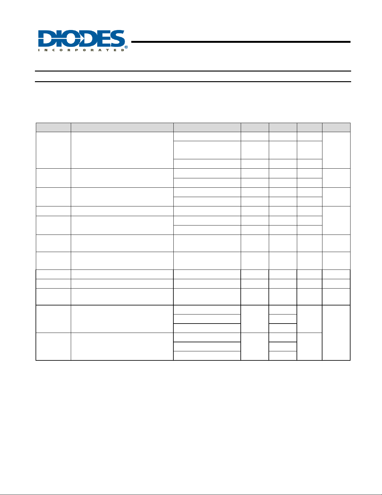
AP78L05/08/12
AP78Lxx Electrical Characteristics (All Output Voltage Versions)
Limits in standard typeface are for T
Unless otherwise specified: I
O
AP78L05
Unless otherwise specified, VIN = 10V
Symbol Parameter Conditions Min Typ. Max Unit
VO
ΔVO
ΔVO
IQ
ΔIQ
VN
ΔVIN/ΔV
IPK
ΔVO/ΔT
V
IN(MIN)
θ
JA
θ
JC
Notes: 4. Recommend 0.01µF minimum load capacitance at output to suppress high frequency noise.
5. Test conditions for TO92: No heat sink, no air flow.
6. Test conditions for SO-8: Device mounted on 2oz copper, minimum recommended pad layout, FR-4 PCB.
7. Test conditions for SOT89: Device mounted on FR-4 substrate PC board, 2oz copper, with minimum recommended pad layout.
Output Voltage
Line Regulation
Load Regulation
Quiescent Current 3 5
Quiescent Current Change
Output Noise Voltage
Ripple Rejection
OUT
Peak Output Current 140 mA
Average Output Voltage Tempco
Minimum Value of Input Voltage
Required to Maintain Line Regulation
Thermal Resistance Junction to
Ambient
Thermal Resistance Junction to Case
AP78L05/08/12
Document number: DS31054 Rev. 10 - 2
= 25℃, Bold typeface applies over T
A
= 40mA, C
= 0.33µF, C
I
AP78LXX SERIES 3-TERMINAL POSITIVE REGULATORS
= -20°C to +125°C for TO92, SOT89 and SO-8 packages.
J
= 0.1µF.
O
4.8 5 5.2
7V ≤ V
1mA ≤ I
1mA ≤ IO ≤ 70mA 4.75
7V ≤ V
8V ≤ V
1mA ≤ IO ≤ 100mA
1mA ≤ IO ≤ 40mA
8V ≤ V
1mA ≤ IO ≤ 40mA
f = 10Hz to 100kHz
(Note 4)
f = 120Hz
8V ≤ V
IO = 5mA
6.7 7 V
TO92 (Note 5)
SO-8 (Note 6) 153
SOT89 (Note 7) 145
TO92 (Note 5)
SO-8 (Note 6) 18
SOT89 (Note 7) 25
www.diodes.com
≤ 20V
IN
O
≤ 20V
IN
≤ 20V
IN
≤ 20V
IN
≤ 16V
IN
4 of 16
≤ 40mA
4.75
5.25
5.25
18 75
10 54
20 60
5 30
1.0
0.1
- 40 µV
47 62 dB
-0.65 mV/
176
33
March 2012
© Diodes Incorporated
V
mV
mV
mA
o
C/W
oC
Page 5
AP78L05/08/12
AP78Lxx Electrical Characteristics (cont.)
AP78L08
Unless otherwise specified, VIN = 14V
Symbol Parameter Conditions Min Typ. Max Unit
VO
ΔVO
ΔVO
IQ
ΔIQ
VN
ΔVIN/ΔV
IPK
ΔVO/ΔT
V
IN(MIN)
θ
JA
θ
JC
Notes: 4. Recommend 0.01µF minimum load capacitance at output to suppress high frequency noise.
5. Test conditions for TO92: No heat sink, no air flow.
6. Test conditions for SO-8: Device mounted on 2oz copper, minimum recommended pad layout, FR-4 PCB.
7. Test conditions for SOT89: Device mounted on FR-4 substrate PC board, 2oz copper, with minimum recommended pad layout.
Output Voltage
Line Regulation
Load Regulation
Quiescent Current 2 5.5
Quiescent Current Change
Output Noise Voltage
Ripple Rejection
OUT
Peak Output Current 140 mA
Average Output Voltage Tempco
Minimum Value of Input Voltage
Required to Maintain Line Regulation
Thermal Resistance Junction to
Ambient
Thermal Resistance Junction to case
AP78LXX SERIES 3-TERMINAL POSITIVE REGULATORS
7.7 8 8.3
10.5V ≤ V
1mA ≤ I
1mA ≤ IO ≤ 70mA 7.6
10.5V ≤ V
11V ≤ V
1mA ≤ I
1mA ≤ IO ≤ 40mA
11V ≤ V
1mA ≤ IO ≤ 40mA
f = 10Hz to 100kHz
(Note 4)
f = 120Hz
13V ≤ V
IO = 5mA
9.7 V
TO92 (Note 5)
SOT89 (Note 7) 157
TO92 (Note 5)
SO-8 (Note 6) 18
SOT89 (Note 7) 33
≤ 23V
IN
≤ 40mA
O
≤ 23V
IN
≤ 23V
IN
≤ 100mA
O
≤ 23V
IN
≤ 23V
IN
7.6
42 175
36 125
18 80
10 40
- 54 µV
37 46 dB
-0.8 mV/
176
33
8.4
8.4
1.5
0.1
mV
mV
mA
o
C/W SO-8 (Note 6) 153
o
C/W
V
oC
AP78L05/08/12
Document number: DS31054 Rev. 10 - 2
5 of 16
www.diodes.com
March 2012
© Diodes Incorporated
Page 6

AP78L05/08/12
AP78Lxx Electrical Characteristics (cont.)
AP78L12
Unless otherwise specified, VIN = 19V
Symbol Parameter Conditions Min Typ. Max Unit
VO
ΔVO
ΔVO
IQ
ΔIQ
VN
ΔVIN/ΔV
IPK
ΔVO/ΔT
V
IN(MIN)
θ
JA
θ
JC
Notes: 5. Test conditions for TO92: No heat sink, no air flow.
6. Test conditions for SO-8: Device mounted on 2oz copper, minimum recommended pad layout, FR-4 PCB.
7. Test conditions for SOT89: Device mounted on FR-4 substrate PC board, 2oz copper, with minimum recommended pad layout.
Output Voltage
Line Regulation
Load Regulation
Quiescent Current 3 5
Quiescent Current Change
Output Noise Voltage 80 µV
Ripple Rejection
OUT
Peak Output Current 140 mA
Average Output Voltage
Tempco
Minimum Value of Input
Voltage Required to Maintain
Line Regulation
Thermal Resistance Junction
to Ambient
Thermal Resistance Junction
to case
AP78LXX SERIES 3-TERMINAL POSITIVE REGULATORS
11.5 12 12.5
14.5V ≤ V
1mA ≤ I
1mA ≤ IO ≤ 70mA 11.4
14.5V ≤ V
16V ≤ V
1mA ≤ I
1mA ≤ IO ≤ 40mA
16V ≤ V
1mA ≤ IO ≤ 40mA
f = 120Hz
15V ≤ V
= 5mA
I
O
13.7 14.5 V
TO92 (Note 5)
SOT89 (Note 7) 145
TO92 (Note 5)
SO-8 (Note 6) 18
SOT89 (Note 7) 25
≤ 27V
IN
≤ 40mA
O
≤ 27V
IN
≤ 27V
IN
≤ 100mA
O
≤ 27V
IN
≤ 25V
IN
11.4
12.6
12.6
30 180
20 110
30 100
10 50
1
0.1
40 54 dB
-1.0 mV/
176
33
mV
mV
mA
o
C/W SO-8 (Note 6) 153
o
C/W
V
oC
AP78L05/08/12
Document number: DS31054 Rev. 10 - 2
6 of 16
www.diodes.com
March 2012
© Diodes Incorporated
Page 7

OUT
PUT CUR
RENT
Q
U
CEN
T CUR
R
N
T
Q
U
CEN
T CUR
REN
T
AP78LXX SERIES 3-TERMINAL POSITIVE REGULATORS
Typical Performance Characteristics
For AP78L05
350
Δ
V = 100mV
T = -25°C
300
250
(mA)
A
T = 25°C
A
OUT
200
T = 150°C
150
A
AP78L05/08/12
4.0
3.8
3.6
(mA)
3.4
E
3.2
3.0
2.8
100
50
0
51015202530
INPUT- OUTPU T DIFFEREN TIAL (V)
Peak Output Current
3.4
3.3
3.2
(mA)
3.1
V = 10V
IN
V = 5V
OUT
I = 40mA
OUT
3.0
2.9
2.8
2.7
IES
2.6
2.5
2.4
-25 0 25 50 75 125
100
JUNCTION TEMPERATURE (°C)
Quiescent Current
2.6
IES
2.4
2.2
2.0
51015202530
V = 5V
OUT
I = 40mA
OUT
T = 25°C
A
INPUT VOLTAG E (V)
Quiescent C ur r ent
100
80
60
40
V = 10V
IN
V = 5V
RIPPLE REJECTION (db)
OUT
20
I = 40mA
OUT
T = 25C
A
0
10 100 1K 100K
10K
FREQUENCY (Hz)
Ripple Rejection
AP78L05/08/12
Document number: DS31054 Rev. 10 - 2
7 of 16
www.diodes.com
March 2012
© Diodes Incorporated
Page 8

AP78L05/08/12
PUT-OUTPU
T
RENT
Typical Performance Characteristics (cont.)
For AP78L05
AP78L05/08/12
Document number: DS31054 Rev. 10 - 2
2.5
I = 40mA
OUT
2.0
IAL (V)
1.5
I = 1mA
DIFFE
OUT
1.0
0.5
DROPOUT CONDITIONS
IN
V = 2% of V
Δ
OUT OUT
0.0
-25 0 25 50 75 125
JUNCTION TEMPERATURE (°C)
I = 70mA
OUT
Dropou t Voltage
AP78LXX SERIES 3-TERMINAL POSITIVE REGULATORS
100
8 of 16
www.diodes.com
March 2012
© Diodes Incorporated
Page 9

OUTPU
T
C
URREN
T
Q
U
C
N
T CUR
R
N
T
2
Q
U
CEN
T CUR
REN
T
NPU
T-OUTPU
T
AP78LXX SERIES 3-TERMINAL POSITIVE REGULATORS
Typical Performance Characteristics
For AP78L08
300
250
(mA)
200
(mA)
E
AP78L05/08/12
2.80
2.75
150
100
50
0
51015202530
INPUT-OUTPUT DIFFERENTIAL (V)
Peak Output Current
3.
3.1
3.0
(mA)
2.9
2.8
2.7
2.6
IES
2.5
2.4
-25 0 25 50 75 125
JUNCTION TEMPERATURE (°C)
Quiesce nt C ur r ent
V = 14V
IN
V = 8V
OUT
I = 40mA
OUT
100
2.71
E
2.67
IES
2.62
10 15 20 25 30
INPUT VOLTAGE (V )
2.5
2.0
(V)
1.5
1.0
I
0.5
0.0
-25 0 25 50 75 125
JUNCTION TEMPERATURE (°C)
Quiesce nt C ur r ent
100
Dropou t Voltage
AP78L05/08/12
Document number: DS31054 Rev. 10 - 2
9 of 16
www.diodes.com
March 2012
© Diodes Incorporated
Page 10

OUTPU
T
C
URRENT
Q
U
CEN
T CUR
REN
T
Q
U
CEN
T CUR
REN
T
NPU
T-OUTPU
T
AP78LXX SERIES 3-TERMINAL POSITIVE REGULATORS
Typical Performance Characteristics (cont.)
For AP78L12
300
AP78L05/08/12
2.960
250
(mA)
200
150
100
50
0
14 18 22 26 30
INPUT-OUTPUT DIFFERENTIAL (V)
Peak Output Current
3.2
3.1
(mA)
3.0
2.9
2.8
V = 19V
IN
V = 12V
OUT
I = 40mA
OUT
2.955
(mA)
2.950
2.945
2.940
IES
2.935
2.930
10 15 20 25 30
INPUT VOLTAGE (V )
2.5
2.0
(V)
1.5
1.0
Quiesce nt C ur r ent
2.7
IES
2.6
2.5
-25 0 25 50 75 125
JUNCTION TEMPERATURE (°C)
Quiescent Current
100
I
0.5
0.0
-25 0 25 50 75 125
JUNCTION TEMPERATURE (°C)
Dropou t Voltage
100
AP78L05/08/12
Document number: DS31054 Rev. 10 - 2
10 of 16
www.diodes.com
March 2012
© Diodes Incorporated
Page 11

A
X
Ordering Information
AP78L05/08/12
AP78LXX SERIES 3-TERMINAL POSITIVE REGULATORS
AP78L XX X X-
Output version
05 : 5V
08 : 8V
12 : 12V
Device
AP78LXXVL-A V TO92 2000/Box -A NA NA
Lead-free
AP78LXXSG-13 S SO-8 NA NA 2500/Tape & Reel -13
AP78LXXYG-13 Y SOT89 NA NA 2500/Tape & Reel -13
Notes: 8. TO92 is available in “Lead Free” product only.
9. SO-8 and SOT89 are available in “Green” products only.
10. Pad layout as shown on Diodes Inc. suggested pad layout document AP02001, which can be found on our website at
http://www.diodes.com/datasheets/ap02001.pdf.
Package
Code
Packaging
(Note 10)
Package Packing
V : TO92
S : SO-8
Y : SOT89
Ammo Box / Tube 13” Tape and Reel
Quantity
Lead Free
L : Lead Free (Note 8)
G : Green (Note 9)
Part Number
Suffix
A :
mmo Box
13 : T ape & Reel
Quantity
Part Number
Suffix
AP78L05/08/12
Document number: DS31054 Rev. 10 - 2
11 of 16
www.diodes.com
March 2012
© Diodes Incorporated
Page 12

Marking Information
(1) TO92
(2) SO-8
AP78L05/08/12
AP78LXX SERIES 3-TERMINAL POSITIVE REGULATORS
( Top View )
Part Number
05 : AP78L05
AP78L XX
Y WWX
123
X
( Top View )
08 : AP78L08
12 : AP78L12
L : Lead Free
Internal code
Xth Week: 01~52
Year : "7" = 2007
"8" = 2008
~
Logo
Part Number
05 : AP78L05
08 : AP78L08
12 : AP78L12
(3) SOT89
AP78L05/08/12
Document number: DS31054 Rev. 10 - 2
8
5
G : Green
: Year : 08, 09,10~
AP78L XX
WW X
YY
X
41
YY
WW : Week : 01~52; 52
represents 52 and 53 week
: Internal Code
X
( Top View )
XX : Identification code
X X
Y W
X
Y : Year : 0~9
: Week : A~Z : 1~26 week;
W
a~z : 27~52 week;
z represents 52 and 53 week
: Internal code
1 32
Device Package Identification Code
AP78L05 SOT89 V2
AP78L08 SOT89 V3
AP78L12 SOT89 V4
X
A~Z : Green
12 of 16
www.diodes.com
March 2012
© Diodes Incorporated
Page 13

AP78LXX SERIES 3-TERMINAL POSITIVE REGULATORS
Package Outline Dimensions (All Dimensions in mm)
(1) Package Type: TO92
E
B
EJECTION
MARK
A
EJECTION
E
MARK
L2
L3
b
L1
e
e
LOOSE PRODUCT
D
c
e2 e2
TAPED PRODUCT
N
(2) TO92 for Ammo pack
AP78L05/08/12
TO92-3L
Dim Min Max Typ
A
3.45 3.66 -
B
4.27 4.78 -
b
D
E
e2
L
L1
L2
L3
N
All Dimensions in mm
- - 0.38
c
- - 0.38
- - 3.87
4.32 4.83
e
- - 1.27
2.40 2.90 -
12.98 15.00 -
12.80 15.00 -
0.80 - -
2.00 3.00 -
1.22 1.37 -
AP78L05/08/12
Document number: DS31054 Rev. 10 - 2
13 of 16
www.diodes.com
March 2012
© Diodes Incorporated
Page 14

AP78LXX SERIES 3-TERMINAL POSITIVE REGULATORS
Package Outline Dimensions (cont.) (All Dimensions in mm)
(3) Package Type: SO-8
E1
E
A1
Detail ‘A’
L
0.254
Gaug e Plan e
Seating Plane
7°~9
A2
e
b
D
A
A3
h
°
45
°
Detail ‘A’
(4) Package Type: SOT89
D1
0
0
2
.
0
R
C
E
H
B1
8
°
B
e
e1
(
4
X
)
L
A
D
AP78L05/08/12
Document number: DS31054 Rev. 10 - 2
14 of 16
www.diodes.com
AP78L05/08/12
SO-8
Dim Min Max
A
A1
A2
A3
b
D
E
E1
e
h
L
θ 0° 8°
All Dimensions in mm
Dim Min Max
A
B
B1
C
D
D1
E
e
e1
H
L
All Dimensions in mm
- 1.75
0.10 0.20
1.30 1.50
0.15 0.25
0.3 0.5
4.85 4.95
5.90 6.10
3.85 3.95
1.27 Typ
- 0.35
0.62 0.82
SOT89
1.40 1.60
0.44 0.62
0.35 0.54
0.35 0.43
4.40 4.60
1.52 1.83
2.29 2.60
1.50 Typ
3.00 Typ
3.94 4.25
0.89 1.20
March 2012
© Diodes Incorporated
Page 15

AP78LXX SERIES 3-TERMINAL POSITIVE REGULATORS
Suggested Pad Layout (All Dimensions in mm)
(1) Package Type: SO-8
X
C1
C2
Y
(2) Package Type: SOT89
X1
Y3
Y
X2 (2x)
Y1
Y4
Y2
C
X (3x)
AP78L05/08/12
Document number: DS31054 Rev. 10 - 2
15 of 16
www.diodes.com
Dimensions Value (in mm)
X 0.60
Y 1.55
C1 5.4
C2 1.27
Dimensions Value (in mm)
X 0.900
X1 1.733
X2 0.416
Y 1.300
Y1 4.600
Y2 1.475
Y3 0.950
Y4 1.125
C 1.500
AP78L05/08/12
March 2012
© Diodes Incorporated
Page 16

AP78L05/08/12
DIODES INCORPORATED MAKES NO WARRANTY OF ANY KIND, EXPRESS OR IMPLIED, WITH REGARDS TO THIS
DOCUMENT, INCLUDING, BUT NOT LIMITED TO, THE IMPLIED WARRANTIES OF MERCHANTABILITY AND FITNESS FOR A
PARTICULAR PURPOSE (AND THEIR EQUIVALENTS UNDER THE LAWS OF ANY JURISDICTION).
Diodes Incorporated and its subsidiaries reserve the right to make modifications, enhancements, improvements, corrections or other
changes without further notice to this document and any product described herein. Diodes Incorporated does not assume any liability
arising out of the application or use of this document or any product described herein; neither does Diodes Incorporated convey any
license under its patent or trademark rights, nor the rights of others. Any Customer or user of this document or products described
herein in such applications shall assume all risks of such use and will agree to hold Diodes Incorporated and all the companies
whose products are represented on Diodes Incorporated website, harmless against all damages.
Diodes Incorporated does not warrant or accept any liability whatsoever in respect of any products purchased through unauthorized
sales channel.
Should Customers purchase or use Diodes Incorporated products for any unintended or unauthorized application, Customers shall
indemnify and hold Diodes Incorporated and its representatives harmless against all claims, damages, expenses, and attorney fees
arising out of, directly or indirectly, any claim of personal injury or death associated with such unintended or unauthorized application.
Products described herein may be covered by one or more United States, international or foreign patents pending. Product names
and markings noted herein may also be covered by one or more United States, international or foreign trademarks.
Diodes Incorporated products are specifically not authorized for use as critical components in life support devices or systems without
the express written approval of the Chief Executive Officer of Diodes Incorporated. As used herein:
A. Life support devices or systems are devices or systems which:
1. are i ntended to implant into the body, or
2. support or sustain life and whose failure to perform when properly used in accordance with instructions for use provided
in the labeling can be reasonably expected to result in significant injury to the user.
B. A critical component is any component in a life support device or system whose failure to perform can be reasonably expected
to cause the failure of the life support device or to affect its safety or effectiveness.
Customers represent that they have all necessary expertise in the safety and regulatory ramifications of their life support devices or
systems, and acknowledge and agree that they are solely responsible for all legal, regulatory and safety-related requirements
concerning their products and any use of Diodes Incorporated products in such safety-critical, life support devices or systems,
notwithstanding any devices- or systems-related information or support that may be provided by Diodes Incorporated. Further,
Customers must fully indemnify Diodes Incorporated and its representatives against any damages arising out of the use of Diodes
Incorporated products in such safety-critical, life support devices or systems.
Copyright © 2012, Diodes Incorporated
www.diodes.com
AP78LXX SERIES 3-TERMINAL POSITIVE REGULATORS
IMPORTANT NOTICE
LIFE SUPPORT
AP78L05/08/12
Document number: DS31054 Rev. 10 - 2
16 of 16
www.diodes.com
March 2012
© Diodes Incorporated
 Loading...