Page 1
4/6 CHANNEL CHARGE PUMP CURRENT SINK FOR LED DRIVER AP3606/AP3607
Data Sheet
General Description
The AP3606 and AP3607 are step-up DC-DC
converters based on 1x/1.5x charge pump and low
dropout current sink, which helps them maintain the
highest efficiency. The AP3606 is specially designed
to drive up to 4 WLEDs in backlight display while
the AP3607 is designed for 6 WLEDs.
These devices provide up to 20mA current for each
WLED. There are totally 16 steps of current control,
which is achieved through a digital pulse dimming
function on EN pin. Additionally, 1MHz high
switching frequency enables the use of small external
capacitors. Internal soft-start circuitry prevents
excessive inrush current during start-up and mode
transition.
The supply voltage ranges of AP3606 and AP3607
are from 2.7V to 5.5V which make them ideally suit
for applications powered by Li-ion battery.
These ICs are available in the tiny package of
QFN-3×3-16.
Features
• Regulated Output Current with ±3% Matching
• Drives up to 4 WLEDs at 20mA Each (AP3606)
Drives up to 6 WLEDs at 20mA Each (AP3607)
• 16 Steps Brightness Control Using Pulse Signal
Dimming
• Wide Operating Voltage Range: 2.7V to 5.5V
• High Operating Frequency: 1MHz
• Auto 1x/1.5x Charge Pump Mode Selection
• Built-in Soft-start
• Output Over Voltage Protection
• Built-in UVLO
• Built-in OTSD
• Operating Temperature Range: -40°C to 85°C
Applications
• Mobile Phone
• PDA
• MP3/4
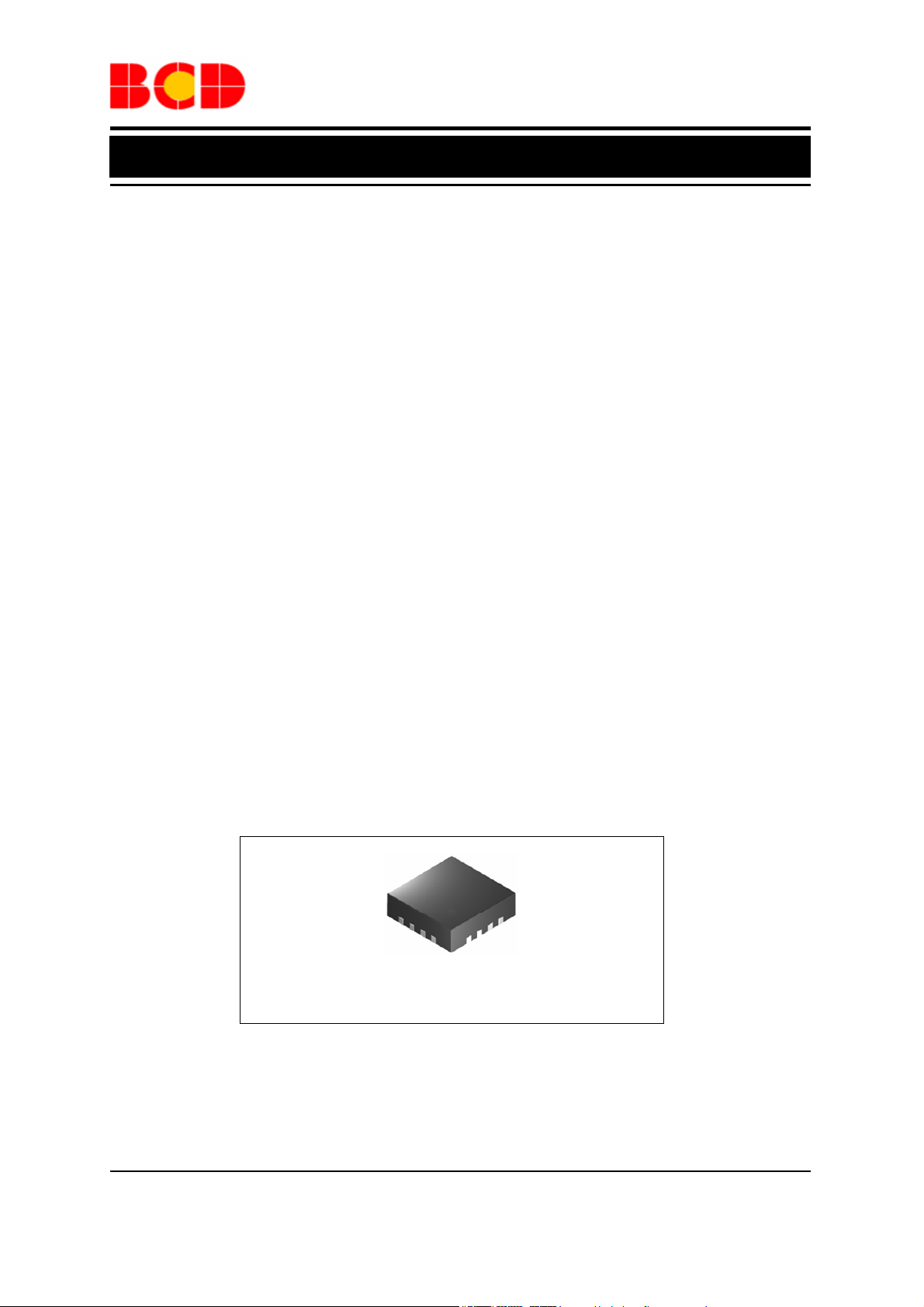
QFN-3×3-16
Figure 1. Package Type of AP3606/AP3607
Jan. 2013 Rev. 1. 5 BCD Semiconductor Manufacturing Limited
1
Page 2
Data Sheet
4/6 CHANNEL CHARGE PUMP CURRENT SINK FOR LED DRIVER AP3606/AP3607
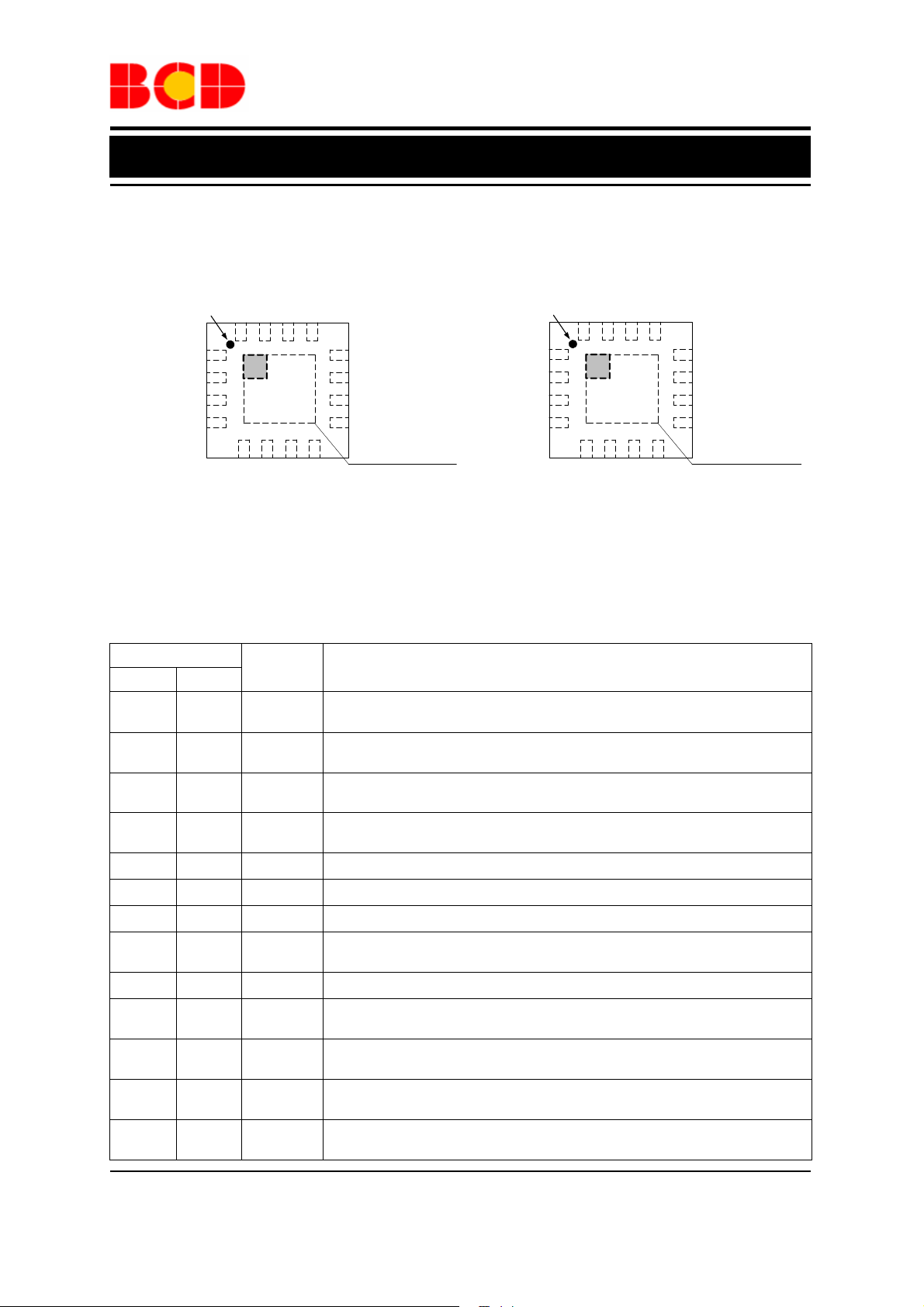
Pin Configuration
FN Package
(QFN-3×3-16)
Pin 1 Mar k
VOUT1
C1-
1
-
C
2
2
C2+
3
49
C1+
5678
NC
EP
VOUT2
D1
13141516
12
D2
11
D3
10
D4
NC
EN
AGND
Note: Pin 14 should be connected with Pin 16 on PCB Board.
VIN
PGND
AP3606 AP3607
Figure 2. Pin Configuration of AP3606/AP3607 (Top View)
Exposed PAD,
Connected to AGND
Pin 1 Ma rk
C1-
-
C
2
C2+
C1+
Note: Pin 15 should be connected with Pin 16 on PCB Board.
VOUT1
VOUT2
D1
1
2
3
49
EP
5678
AGND
D2
13141516
12
D3
11
D4
10
D5
D6
Exposed PAD,
Connected to AGND
EN
VIN
PGND
Pin Description
Pin Number
AP3606 AP3607
1 1 C1-
2 2 C2-
3 3 C2+
4 4 C1+
5 5 AGND Analog ground
6 6 PGND Power ground
7 7 VIN Supply voltage input
8 8 EN
9, 15
9, 10 D6 , D5
10, 11, 12,
Jan. 2013 Rev. 1. 5 BCD Semiconductor Manufacturing Limited
11, 12, 13,
13
14
14 15 VOUT2
16 16 VOUT1
Pin Name Function
Flying capacitor 1 negative terminal. The flying capacitor should be connected as
close to this pin as possible
Flying capacitor 2 negative terminal. The flying capacitor should be connected as
close to this pin as possible
Flying capacitor 2 positive terminal. The flying capacitor should be connected as
close to this pin as possible
Flying capacitor 1 positive terminal. The flying capacitor should be connected as
close to this pin as possible
Enable control input. Logic high enables the IC; while logic low forces the IC into
shutdown mode. It is used for digital dimming by applying a pulse signal on it.
NC No connection (AP3606 only)
Current sink for WLED6 and WLED5. Connect the cathode of WLEDs to these
pins. If not used, these pins must be connected with VIN (AP3607 only)
D4 ~ D1
Current sink for WLED4, 3, 2, 1. Connect the cathode of WLEDs to these pins. If
not used, these pins must be connected with VIN
Output pin 2. It powers 4 channels current sink (AP3606) and 6 channels current
sink (AP3607)
Output Pin 1. It’s the charge pump output. The output capacitor should be placed
closely to this pin
2
Page 3
Data Sheet
4/6 CHANNEL CHARGE PUMP CURRENT SINK FOR LED DRIVER AP3606/AP3607
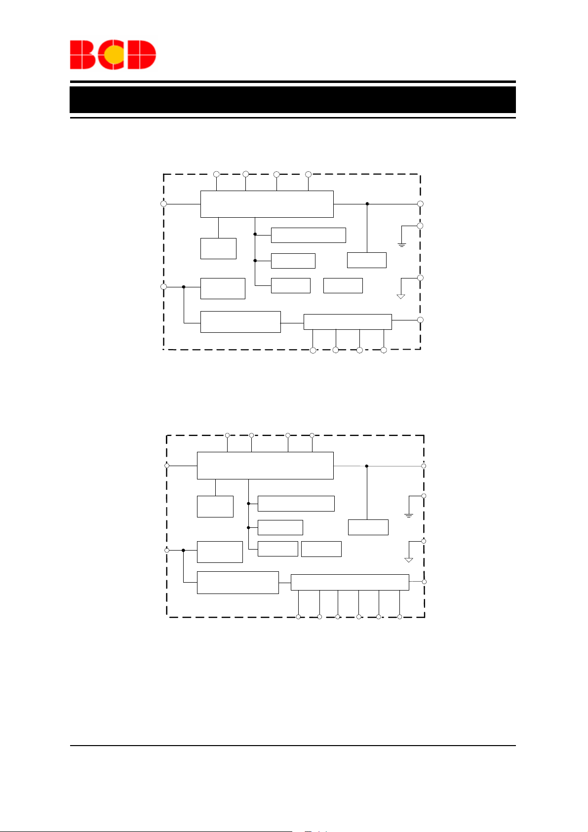
Functional Block Diagram
C1- C1+ C2- C2+
VIN
EN
7
8
14 32
1x/1.5x Charge Pump
1MHz
OSC
Shutdown
Delay
16 Steps Pulse
Dimming Controller
Current Limitation
Soft Start
UVLO
4 Channels Current Sink
AP3606
OVP
OTSD
2D1 D3 D4
D
16
VOUT1
5
AGND
6
PGND
14
VOUT2
10111213
VIN
EN
7
8
1MHz
OSC
Shutdown
Delay
16 Steps Pulse
Dimming Controller
Figure 3. Functional Block Diagram of AP3606/AP3607
C1+
C1-
1
1x /1.5x Charge Pump
C2- C2+
Soft Start
UVLO
2
OTSD
4
Current Limitation
6 Channels Current Sink
D2 D3 D4 D5 D6
D1
AP3607
3
16
VOUT1
5
AGND
OVP
11121314
6
PGND
15
VOUT2
910
Jan. 2013 Rev. 1. 5 BCD Semiconductor Manufacturing Limited
3
Page 4
Data Sheet
4/6 CHANNEL CHARGE PUMP CURRENT SINK FOR LED DRIVER AP3606/AP3607
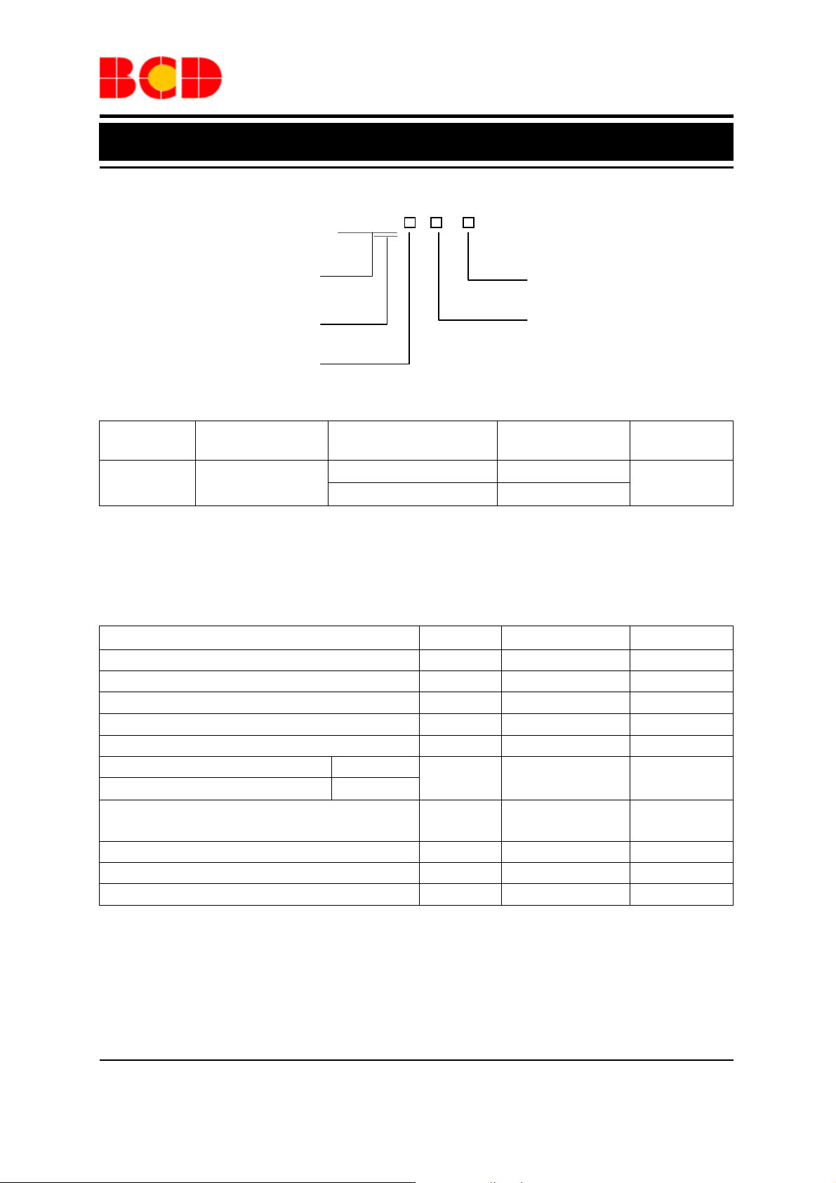
Ordering Information
AP36XX -
Circuit Type G1: Green
06: AP3606
07: AP3607
Package
FN: QFN-3×3-16
Package
QFN-3×3-16
Temperature
Range
-40 to 85°C
Part Number Marking ID
AP3606FNTR-G1 B1B
AP3607FNTR-G1 B1C
BCD Semiconductor's Pb-free products, as designated with "G1" suffix in the part number, are RoHS compliant
and green.
TR: Tape and Reel
Packing
Type
Tape & Reel
Absolute Maximum Ratings (Note 1)
Parameter Symbol Value Unit
Input Voltage VIN -0.3 to 6 V
VOUT Pin Voltage (VOUT1 & VOUT2) V
EN Pin Voltage VEN -0.3 to 6 V
C1+, C2+ Pin Voltage VC+ -0.3 to 6 V
C1-, C2- Pin Voltage VC- -6 to 0.3 V
D1, D2, D3, D4 Pin Voltage AP3606
D1, D2, D3, D4, D5, D6 Pin Voltage AP3607
Thermal Resistance
(Junction to Ambient, No Heat Sink, Free Air)
Operating Junction Temperature
Storage Temperature
Lead Temperature (Soldering, 10sec)
Note 1: Stresses greater than those listed under “Absolute Maximum Ratings” may cause permanent damage to
the device. These are stress ratings only, and functional operation of the device at these or any other conditions
beyond those indicated under “Recommended Operating Conditions” is not implied. Exposure to “Absolute
Maximum Ratings” for extended periods may affect device reliability.
-6 to 0.3 V
OUT
V
V
D
θJA
T
J
T
STG
T
LEAD
to VIN V
OUT
60 ºC/W
150 ºC
-65 to 150 ºC
260 ºC
Jan. 2013 Rev. 1. 5 BCD Semiconductor Manufacturing Limited
4
Page 5

Data Sheet
4/6 CHANNEL CHARGE PUMP CURRENT SINK FOR LED DRIVER AP3606/AP3607
Recommended Operating Conditions
Parameter Symbol Min Max Unit
Input Voltage VIN 2.7 5.5 V
Operating Ambient Temperature TA -40 85 ºC
Electrical Characteristics
=3.6V, VEN=VIN, TA=25ºC, CIN=C1=C2=C
V
IN
=1μF, VF(forward voltage)=3.2V, unless otherwise noted.
OUT
Parameter Symbol Conditions Min Typ Max Unit
Input Section
Input Voltage VIN ID=0mA to 80mA 2.7 5.5 V
Under Voltage Lockout Threshold VIN Falling 2.2 V
Under Voltage Lockout Hysteresis 250 mV
Supply Current ICC No Load 1.7 3 mA
Shutdown Supply Current I
Charge Pump Section
Switch Frequency f
1x Mode to 1.5x Mode Transition
Voltage (V
1.5x Mode to 1x Mode Transition
Voltage (V
Current Source Section
Falling)
IN
Rising)
IN
VEN=GND 3 10
SHDN
VIN=3.0V, 1.5x Mode 0.7 1 1.3 MHz
OSC
=3.2V,
V
D
I
D1=ID2=ID3=ID4
=3.2V,
V
D
I
D1=ID2=ID3=ID4
=20mA
I
D5=ID6
V
=3.2V,
D
I
D1=ID2=ID3=ID4
=3.2V,
V
D
I
D1=ID2=ID3=ID4
=20mA
I
D5=ID6
=20mA
3.5 3.6 V
=
=20mA
3.7 3.8 V
=
V
V1X
1.5X
AP3606
AP3607
AP3606
AP3607
μA
100% Setting,
WLED Current ID
3.0V≤VIN≤5.0V
=-40ºC to 85ºC
T
A
18.5 20 21.5 mA
Jan. 2013 Rev. 1. 5 BCD Semiconductor Manufacturing Limited
5
Page 6
Data Sheet
4/6 CHANNEL CHARGE PUMP CURRENT SINK FOR LED DRIVER AP3606/AP3607
Electrical Characteristics (Continued)
=3.6V, VEN=VIN, TA=25ºC, CIN=C1=C2=C
V
IN
Parameter Symbol Conditions Min Typ Max Unit
Current Matching Between any
Two Outputs
Current Matching Between any
Two Outputs
I
D-Match1
I
D-Match2
=1μF, VF(forward voltage)=3.2V, unless otherwise noted.
OUT
AP3606
AP3607
AP3606
AP3607
V
D1=VD2=VD3=VD4
3.2V
V
D1=VD2=VD3=VD4
VD5=VD6=3.2V
V
D1=VD2=VD3=VD4
V to 4.0V
VIN=3.2V to 5.0V
V
D1=VD2=VD3=VD4
VD5=VD6=3.0V to 4.0V
=
=
=3.0
=
-3 3 %
-3.5 3.5 %
VIN=3.2V to 5.0V
Enable Section
EN High Level Threshold Voltage VIH 1.5 V
EN Low Level Threshold Voltage VIL 0.5 V
EN Input Current IEN VEN= 0V to 5V 1 10
EN Low to Shutdown Delay t
EN Low Time for Dimming tLO
EN High Time for Dimming tHI
1 ms
SHDN
0.45 500
0.45
μA
μs
μs
Total Device
Soft-start Time tSS
AP3606 I
=80mA Total
D
200
μs
AP3607 ID=120mA Total
=3.2V,
V
Inrush Current I
Over Voltage Protection V
Thermal Shutdown T
AP3606
INRUSH
AP3607
Note 2 5.5 V
OVP
160 ºC
OTSD
IN
I
=80mA Total
D
=3.2V,
V
IN
=120mA Total
I
D
200
mA
320
Thermal Shutdown Hysteresis T
Thermal Resistance
(Junction to Case)
20 ºC
HYS
θ
QFN-3×3-16 15 ºC/W
JC
Note 2: Open circuit at any WLED that is programmed to be in the on state.
Jan. 2013 Rev. 1. 5 BCD Semiconductor Manufacturing Limited
6
Page 7

Data Sheet
4/6 CHANNEL CHARGE PUMP CURRENT SINK FOR LED DRIVER AP3606/AP3607
Typical Performance Characteristics
=25ºC, CIN=C1=C2=C
T
A
=1μF, VF=3.2V, unless otherwise noted.
OUT
4.0
3.5
3.0
2.5
2.0
Shutdown Supply Current (μA)
1.5
1.0
-40 -20 0 20 40 60 80 100 120 140
F igure 4. Sh utdo wn Supply Current vs. Temperature Figure 5. Shutdown Supply Current vs. Temperature
Temperature (OC)
AP3606
VIN=3.2V
Shut Down
4.0
3.5
3.0
2.5
2.0
Shutdown Supply Current (μA)
1.5
1.0
-40 -20 0 20 40 60 80 100 120 140
Temperature (oC)
AP3607
VIN=3.6V
Shut Down
2.2
2.0
1.8
1.6
1.4
Quiescent Current (mA)
1.2
1.0
-40 -20 0 20 40 60 80 100 120 140
Temperature (OC)
AP3606/AP3607
TA=25oC
VIN=5V
No Load
1x Mode
Figure 6. 1x Mode Quiescent Current vs. Temperature
4.4
4.0
3.6
3.2
2.8
Quiescent Current (mA)
2.4
2.0
-40 -20 0 20 40 60 80 100 120 140
Temperature (OC)
AP3606/AP3607
TA=25oC
VIN=3.2V
No Load
1.5x Mode
Figure 7. 1.5x Mode Quiescent Current
vs. Temperature
Jan. 2013 Rev. 1. 5 BCD Semiconductor Manufacturing Limited
7
Page 8

Data Sheet
4/6 CHANNEL CHARGE PUMP CURRENT SINK FOR LED DRIVER AP3606/AP3607
Typical Performance Characteristics (Continued)
TA=25ºC, CIN=C1=C2=C
=1μF, VF=3.2V, unless otherwise noted.
OUT
22
WLED Current (mA)
AP3606
21
VIN=5V
TA=25OC
20
19
18
17
16
-40-200 20406080100120140
Temperature (OC)
22
AP3606
21
VIN=3.2V
TA=25OC
20
I
D1
I
D2
I
D3
I
D4
19
18
WLED Current (mA)
17
16
-40 -20 0 20 40 60 80 100 120 140
Figure 8. 1x Mode WLED Current vs. Temperature Figure 9. 1.5x Mode WLED Current vs. Temperature
22
AP3607
21
TA=25oC
VIN=5V
20
19
18
WLED Current (mA)
17
16
-40 -20 0 20 40 60 80 100 120 140
Figure 10. 1x Mode WLED Current vs. Temperature
Temperature (OC)
22
AP3607
TA=25oC
21
VIn =3.6V
20
I
D1
I
D2
I
D3
I
D4
I
D5
I
D6
19
18
WLED Current (mA)
17
16
-40 -20 0 20 40 60 80 100 120 140
Figure 11. 1.5x Mode WLED Current vs.
Temperature (OC)
Temperature (OC)
Temperature
I
D1
I
D2
I
D3
I
D4
I
D1
I
D2
I
D3
I
D4
I
D5
I
D6
Jan. 2013 Rev. 1. 5 BCD Semiconductor Manufacturing Limited
8
Page 9

Data Sheet
4/6 CHANNEL CHARGE PUMP CURRENT SINK FOR LED DRIVER AP3606/AP3607
Typical Performance Characteristics (Continued)
TA=25ºC, CIN=C1=C2=C
22
21
20
19
18
WLED Current (mA)
AP3606
TA=25OC
17
V
Falling
IN
16
2.83.23.64.04.44.85.25.6
Figure 12. WLED Current vs. Input Voltage Figure 13. WLED Current vs. Input Voltage
1.4
1.2
1.0
0.8
Frequency (MHz)
0.6
0.4
-40 -20 0 20 40 60 80 100 120 140
Figure 14. Frequency vs. Temperature Figure 15. Frequency vs. Temperature
=1μF, VF=3.2V, unless otherwise noted.
OUT
I
D1
I
D2
I
D3
I
D4
Input Voltage (V)
AP3606
VIN=3.6V
ID1=ID2=ID3=ID4=20mA
Temperature(oC)
22
21
20
19
18
WLED Current (mA)
AP3607
TA=25oC
17
VIN Falling
16
2.83.23.64.04.44.85.25.6
1.4
1.2
1.0
0.8
Frequency (MHz)
0.6
0.4
-40 -20 0 20 40 60 80 100 120 140
Input Voltage (V)
AP3607
VIN=3.6V
ID1=ID2=ID3=ID4=ID5=ID6=20mA
Temperature (oC)
I
D1
I
D2
I
D3
I
D4
I
D5
I
D6
Jan. 2013 Rev. 1. 5 BCD Semiconductor Manufacturing Limited
9
Page 10

Data Sheet
4/6 CHANNEL CHARGE PUMP CURRENT SINK FOR LED DRIVER AP3606/AP3607
Typical Performance Characteristics (Continued)
TA=25ºC, CIN=C1=C2=C
2.2
2.0
1.8
1.6
1.4
Quiescent Current (mA)
1.2
1.0
2.02.53.03.54.04.55.05.5
Figure 16. 1x Mode Quiescent Current vs. Figure 17. UVLO Threshold Voltage vs. Te mperature
Input Voltage
100
90
80
70
60
50
Efficiency (%)
40
30
20
10
2.8 3.2 3.6 4.0 4.4 4.8 5.2 5.6
=1μF, VF=3.2V, unless otherwise noted.
OUT
AP3606/AP3607
TA=25oC
No Load
VIN Rising
Input Voltage (V)
AP3606
TA=25oC
VIN from High to Low
ID1=ID2=ID3=ID4=20mA
Input Voltage (V)
2.6
2.5
2.4
2.3
2.2
2.1
UVLO Threshold Vol tage (V)
2.0
1.9
-40 -20 0 20 40 60 80 100 120 140
100
90
80
70
60
50
Efficiency (%)
40
30
20
10
2.8 3.2 3.6 4.0 4.4 4.8 5.2 5.6
Power Falling
Power Rising
Temperature (oC)
AP3607
TA=25oC
V
from High to Low
IN
ID1=ID2=ID3=ID4=ID5=ID6=20mA
Input Voltage (V)
AP3606/AP3607
TA=25oC
No Load
Figure 18. Efficiency vs. Input Voltage Figure 19. Efficiency vs. Input Voltage
Jan. 2013 Rev. 1. 5 BCD Semiconductor Manufacturing Limited
10
Page 11

Data Sheet
4/6 CHANNEL CHARGE PUMP CURRENT SINK FOR LED DRIVER AP3606/AP3607
Typical Performance Characteristics (Continued)
TA=25ºC, CIN=C1=C2=C
=1μF, VF=3.2V, unless otherwise noted.
OUT
V
C1+
2V/div
V
OUT
1V/div
V
EN
2V/div
I
IN
0.2A/div
Figure 20. 1x Mode Turn on Characteristic Figure 21. 1x Mode Turn off Characteristic
Time (100μs/div) Time (400μs/div)
(AP3606) (AP3606)
V
2V/div
V
1V/div
2V/div
0.2A/div
V
C1+
OUT
EN
I
IN
V
C1+
2V/div
V
OUT
1V/div
V
EN
2V/div
I
IN
0.2A/div
Figure 22. 1x Mode Turn on Characteristic Figure 23. 1x Mode Turn off Characteristic
Jan. 2013 Rev. 1. 5 BCD Semiconductor Manufacturing Limited
Time (100μs/div) Time (400μs/div)
(AP3607) (AP3607)
2V/div
1V/div
2V/div
0.2A/div
11
V
C1+
V
OUT
V
EN
I
IN
Page 12

Data Sheet
4/6 CHANNEL CHARGE PUMP CURRENT SINK FOR LED DRIVER AP3606/AP3607
Typical Performance Characteristics (Continued)
TA=25ºC, CIN=C1=C2=C
V
C1+
2V/div
1V/div
2V/div
0.2A/div
V
OUT
V
EN
I
IN
Figure 24. 1.5x Mode Turn on Characteristic Figure 25. 1.5x Mode Turn off Characteristic
=1μF, VF=3.2V, unless otherwise noted.
OUT
V
C1+
2V/div
V
OUT
1V/div
V
EN
2V/div
I
IN
0.2A/div
Time (100μs/div)
(AP3606) (AP3606)
Time (400μs/div)
V
C1+
2V/div
V
OUT
1V/div
V
EN
2V/div
I
IN
0.2A/div
Figure 26. 1.5x Mode Turn on Characteristic Figure 27. 1.5x Mode Turn off Characteristic
Time (100μs/div)
(AP3607) (AP3607)
V
C1+
2V/div
V
OUT
1V/div
V
EN
2V/div
I
0.2A/div
IN
Time (400μs/div)
Jan. 2013 Rev. 1. 5 BCD Semiconductor Manufacturing Limited
12
Page 13

Data Sheet
4/6 CHANNEL CHARGE PUMP CURRENT SINK FOR LED DRIVER AP3606/AP3607
Typical Performance Characteristics (Continued)
TA=25ºC, CIN=C1=C2=C
=1μF, VF=3.2V, unless otherwise noted.
OUT
V
VEN
2V/div
EN
2V/div
I
WLED
5mA/div
I
WLED
5mA/div
V
20mV/div
I
20mA/div
V
OUT
50mV/div
V
C1+
2V/div
Time (2ms/div)
Figure 28. 1x Mode Dimming Operation Figure 29. 1x Mode Dimming Operation
( AP3606, VIN=5V, fEN=2kHz) (AP3607, VIN=5V, f
I
IN
IN
20mA/div
V
20mV/div
V
OUT
50mV/div
V
2V/div
IN
IN
C1+
Time (2ms/div)
=2kHz)
EN
Figure 30. Output Ripple Figure 31. Output Ripple
(AP3606, VIN=3.3V, ID=80mA) (AP3607, VIN=3.3V, I
Time (400ns/div) Time (400ns/div)
=120mA)
D
Jan. 2013 Rev. 1. 5 BCD Semiconductor Manufacturing Limited
13
Page 14

Data Sheet
4/6 CHANNEL CHARGE PUMP CURRENT SINK FOR LED DRIVER AP3606/AP3607
Digital Dimming Operating Diagram
Figure 32. Digital Dimming Operating Diagram of AP3606/AP3607
Note 3: The dimming control can be achieved by applying a pulse to the EN pin. When the low level duration
time of pulse is between T
will decrease 1/16. If the low level duration time is larger than T
AP3606/AP3607 is powered on, the WLED is in full brightness. And it will keep maximum current until the
pulse is detected. After 15 pulses the WLED current decreases to 1/16 of full brightness. It will increase to full
brightness if a pulse is added to EN pin then.
LOmin
and T
, and the high level duration time is larger than T
LOmax
SHDNmax,
the IC will be turned off. When
, the LED current
HImin
Jan. 2013 Rev. 1. 5 BCD Semiconductor Manufacturing Limited
14
Page 15

Data Sheet
4/6 CHANNEL CHARGE PUMP CURRENT SINK FOR LED DRIVER AP3606/AP3607
Typical Application
3 WLEDs
4 WLEDs
Jan. 2013 Rev. 1. 5 BCD Semiconductor Manufacturing Limited
15
Page 16

Data Sheet
4/6 CHANNEL CHARGE PUMP CURRENT SINK FOR LED DRIVER AP3606/AP3607
Typical Application (Continued)
5 WLEDs
C1 1 F C2 1 F
D1 D2 D3 D4 D5 D6
3
2
4
C2+
C1-1C1+
7
VIN
Li-ion
Battery
C
1 F
Pulse Input
IN
C
OUT
1 F
8
EN
15
VOUT2
16
VOUT1
5
AGND
6 WLEDs
Figure 33. Typical Applications of AP3606/AP3607
C2-
AP3607
PGND
6
14
D1
13
D2
12
D3
11
D4
10
D5
9
D6
Detailed application information, please refer to AP3606/AP3607 application note.
Jan. 2013 Rev. 1. 5 BCD Semiconductor Manufacturing Limited
16
Page 17

Data Sheet
4/6 CHANNEL CHARGE PUMP CURRENT SINK FOR LED DRIVER AP3606/AP3607
Mechanical Dimensions
QFN-3×3-16 Unit: mm(inch)
Jan. 2013 Rev. 1. 5 BCD Semiconductor Manufacturing Limited
17
Page 18

BCD Semiconductor Manufacturing Limited
IMPORTANT NOTICE
IMPORTANT NOTICE
BCD Semiconductor Manufacturing Limited reserves the right to make changes without further notice to any products or specifi-
BCD Semiconductor Manufacturing Limited reserves the right to make changes without further notice to any products or specifi-
cations herein. BCD Semiconductor Manufacturing Limited does not assume any responsibility for use of any its products for any
cations herein. BCD Semiconductor Manufacturing Limited does not assume any responsibility for use of any its products for any
particular purpose, nor does BCD Semiconductor Manufacturing Limited assume any liability arising out of the application or use
particular purpose, nor does BCD Semiconductor Manufacturing Limited assume any liability arising out of the application or use
of any its products or circuits. BCD Semiconductor Manufacturing Limited does not convey any license under its patent rights or
of any its products or circuits. BCD Semiconductor Manufacturing Limited does not convey any license under its patent rights or
other rights nor the rights of others.
other rights nor the rights of others.
http://www.bcdsemi.com
MAIN SITE
MAIN SITE
- Headquarters
BCD Semiconductor Manufacturing Limited
BCD Semiconductor Manufactur ing Limited
- Wafer Fab
No. 1600, Zi Xing Road, Shanghai ZiZhu Science-based Industrial Park, 200241, China
Shanghai SIM-BCD Semiconductor Manufacturing Limited
Tel: +86-21-24162266, Fax: +86-21-24162277
800, Yi Shan Road, Shanghai 200233, China
Tel: +86-21-6485 1491, Fax: +86-21-5450 0008
REGIONAL SALES OFFICE
Shenzhen Office
REGIONAL SALES OFFICE
Shanghai SIM-BCD Semiconductor Manufacturing Co., Ltd., Shenzhen Office
Shenzhen Office
Unit A Room 1203, Skyworth Bldg., Gaoxin Ave.1.S., Nanshan District, Shenzhen,
Shanghai SIM-BCD Semiconductor Manufacturing Co., Ltd. Shenzhen Office
China
Advanced Analog Circuits (Shanghai) Corporation Shenzhen Office
Tel: +86-755-8826 7951
Room E, 5F, Noble Center, No.1006, 3rd Fuzhong Road, Futian District, Shenzhen 518026, China
Fax: +86-755-8826 7865
Tel: +86-755-8826 7951
Fax: +86-755-8826 7865
- Wafer Fab
BCD Semiconductor Manufacturing Limited
Shanghai SIM-BCD Semiconductor Manufacturing Co., Ltd.
- IC Design Group
800 Yi Shan Road, Shanghai 200233, China
Advanced Analog Circuits (Shanghai) Corporation
Tel: +86-21-6485 1491, Fax: +86-21-5450 0008
8F, Zone B, 900, Yi Shan Road, Shanghai 200233, China
Tel: +86-21-6495 9539, Fax: +86-21-6485 9673
Taiwan Office
BCD Semiconductor (Taiwan) Company Limited
Taiwan Office
4F, 298-1, Rui Guang Road, Nei-Hu District, Taipei,
BCD Semiconductor (Taiwan) Company Limited
Tai wan
4F, 298-1, Rui Guang Road, Nei-Hu District, Taipei,
Tel: +886-2-2656 2808
Taiwan
Fax: +886-2-2656 2806
Tel: +886-2-2656 2808
Fax: +886-2-2656 2806
USA Office
BCD Semiconductor Corp.
USA Office
30920 Huntwood Ave. Hayward,
BCD Semiconductor Corporation
CA 94544, USA
30920 Huntwood Ave. Hayward,
Tel : +1-510-324-2988
CA 94544, U.S.A
Fax: +1-510-324-2788
Tel : +1-510-324-2988
Fax: +1-510-324-2788
 Loading...