

Page 1

Data Sheet
100mA REGULATED CHARGE PUMP AP3602A/B
General Description
The AP3602A/B are regulated step-up DC/DC
converters based on charge pump technique. These ICs
have the ability to supply 100mA constant output
current or 250mA peak output current for 100ms from
3.0V to 5V input (2.7V to 4.5 V for AP3602B), so they
can be used as white LEDs driver or flash LED driver.
The AP3602A/B have very low power dissipation and
high efficiency in typical applications. Other features
include over-temperature protection, low temperature
coefficient and etc. to meet some special requirements
of hand-held battery powered devices.
Only 3 external capacitors are required in applications,
which helps to save space and lower cost. These chips
also have a disable terminal to turn on or turn off the
chip to ease the use.
The AP3602A/B are available in SOT-23-6 package.
Features
· Low Quiescent Current: 13μA Typical
· Regulated Output Voltage Precision: 4%
· High Output Current:
100mA when V
50mA when V
· High Frequency: up to 1.2 MHz
· Low Shutdown Supply Current: <1
· High Output Peak Current: 250mA for 100ms
· Over Temperature Protection
· Operating Temperature Range: -40
IN
≥2.7V
IN
≥3.0V
μA
o
C to 85oC
Applications
· Mobile Phone Backlight Driver
· Camera Flash LED Driver
· MP3, MP4
· Handheld Device
· Portable Communication Device
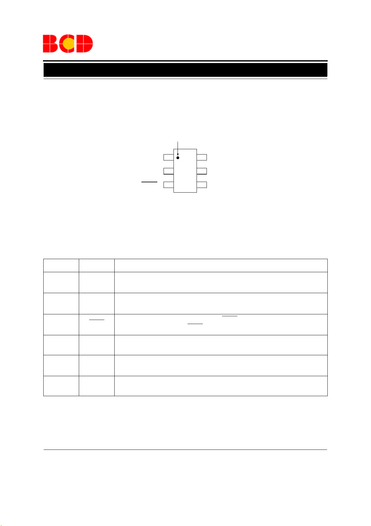
SOT-23-6
Figure 1. Package Type of AP3602A/B
Dec. 2012 Rev. 2. 0 BCD Semiconductor Manufacturing Limited
1
Page 2
Data Sheet
1
2
34
5
Pin 1 Mark
6
100mA REGULATED CHARGE PUMP AP3602A/B
Pin Configuration
K Package
(SOT-23-6)
V
OUT
GND
SHDN
C+
V
C-
IN
Figure 2. Pin Configuration of AP3602A/B (Top View)
Pin Description
Pin Number Pin Name Function
1
V
OUT
2 GND
3 SHDN
Regulated Output Voltage. V
capacitor which is placed as close to the pin as possible for best performance
Ground. GND should be tied to a ground plane for best performance. The C
should be placed as close to this pin as possible
Active Low Shutdown Input. A low signal on SHDN disables the AP3602A/B, while a high
signal enables the AP3602A/B. SHDN
should be bypassed with a 1μF to 22μF low ESR ceramic
OUT
pin must not be allowed to float
OUT
and C
IN
4C-
5
6C+
Dec. 2012 Rev. 2. 0 BCD Semiconductor Manufacturing Limited
Flying Capacitor Negative Terminal. The flying capacitor should be placed as close to this pin
as possible
IN
which is placed as close to the pin as possible for best performance
Input Supply Voltage. V
V
should be bypassed with a 1μF to 22μF low ESR ceramic capacitor
IN
Flying Capacitor Positive Terminal. The flying capacitor should be placed as close to this pin
as possible
2
Page 3
Data Sheet
3
5
4
2
1
1.25V
OSC
6
S3
S4
S1
S2
COMP
EN
R1
R2
CONTROL
+
-
OTP
100mA REGULATED CHARGE PUMP AP3602A/B
Functional Block Diagram
V
IN
SHDN
Ordering Information
Circuit Type
Output Voltage
A: 5V
B: 4.5V
Figure 3. Functional Block Diagram of AP3602A/B
AP3602
-
E1: RoHS
G1: Green
TR: Tape and Reel
Package
K: SOT-23-6
C+
C-
V
OUT
GND
Package
SOT-23-6
BCD Semiconductor's products as designated with "E1" suffix in the part number are RoHS compliant. Products with "G1" suffix are available in green packages.
Temperature
Range
-40 to 85
AP3602AKTR-E1 AP3602AKTR-G1 E7T G7T Tape & Reel
o
C
AP3602BKTR-E1 AP3602BKTR-G1 E8T G8T Tape & Reel
Part Number Marking ID
RoHS Green RoHS Green
Packing Type
Dec. 2012 Rev. 2. 0 BCD Semiconductor Manufacturing Limited
3
Page 4
Data Sheet
100mA REGULATED CHARGE PUMP AP3602A/B
Absolute Maximum Ratings (Note 1)
Parameter Symbol Value Unit
Input Voltage V
Output Voltage V
SHDN
Pin Voltage V
Thermal Resistance (Junction to Ambient, no Heat sink) R
Operating Junction Temperature T
Storage Temperature Range T
Lead Temperature (Soldering, 10sec) T
IN
O
SHDN
θJA
J
STG
LEAD
7V
7V
7V
300
150
-65 to 150
260
o
C/W
o
o
o
C
C
C
ESD (Human Body Model) 2000 V
Note 1: Stresses greater than those listed under "Absolute Maximum Ratings" may cause permanent damage to
the device. These are stress ratings only, and functional operation of the device at these or any other conditions
beyond those indicated under "Recommended Operating Conditions" is not implied. Exposure to "Absolute Maximum Ratings" for extended periods may affect device reliability.
Recommended Operating Conditions
Parameter Symbol Min Max Unit
Input Voltage
V
IN
Operating Temperature T
Dec. 2012 Rev. 2. 0 BCD Semiconductor Manufacturing Limited
AP3602A 2.7 5
AP3602B 2.7 4.5
A
-40 85
4
V
o
C
Page 5

Data Sheet
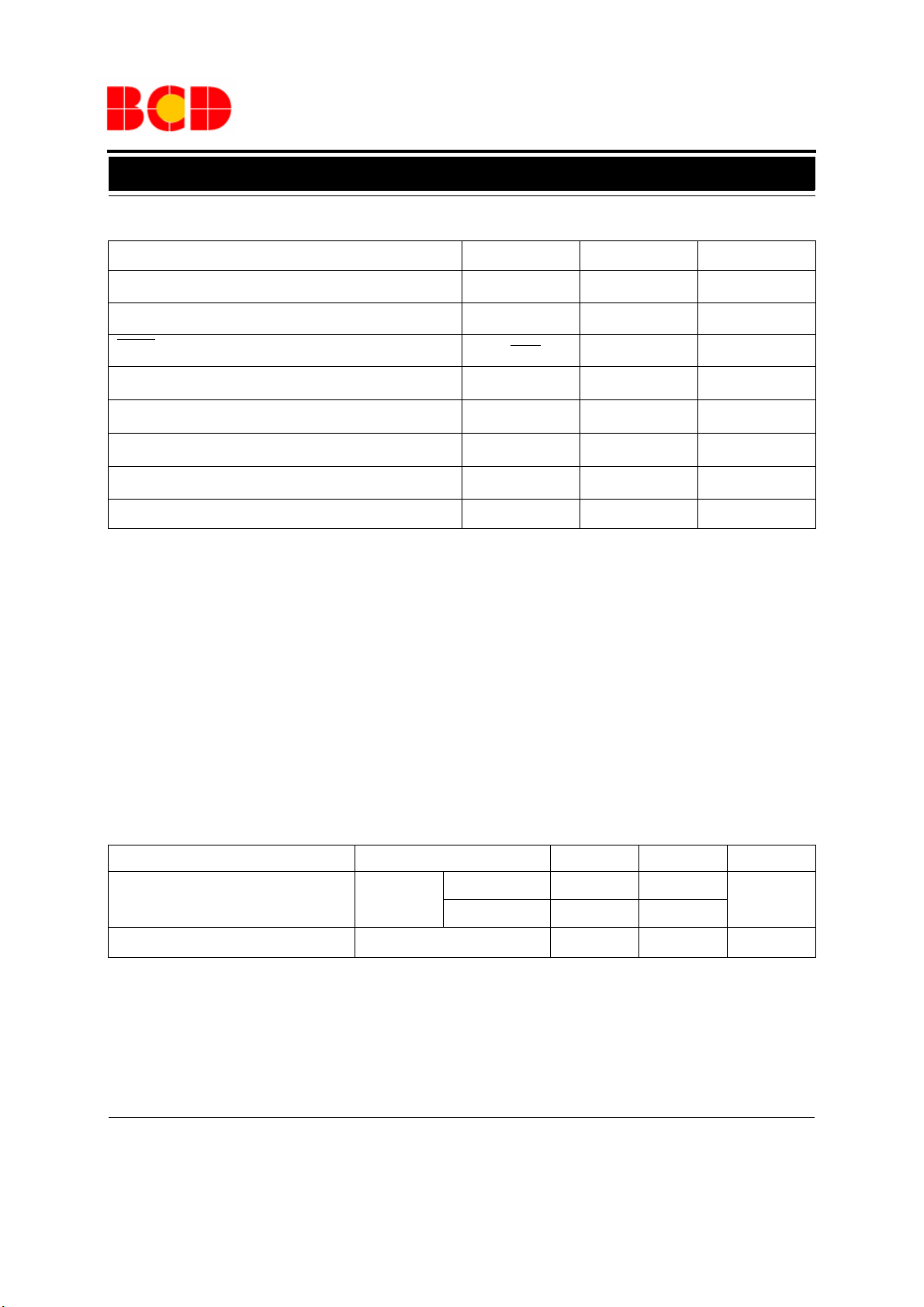
100mA REGULATED CHARGE PUMP AP3602A/B
Electrical Characteristics
(C
FLY
=1μF, CIN=C
=10μF, TA=25
OUT
o
C, unless otherwise specified.)
For AP3602A
Parameter Symbol Conditions Min Typ Max Unit
Input Voltage V
Quiescent Current
Output Voltage
Shutdown Supply Current
Ripple Voltage
I
V
RIPPLE
Efficiency
Frequency f
SHDN
Input Threshold
High
SHDN
Input Threshold
Low
Input Current High I
SHDN
Input Current Low I
SHDN
V
Turn-on Time t
OUT
Short-Circuit Current I
IN
I
Q
V
O
SHDN
η
OSC
V
IH
V
IL
IH
IL
ON
SC
VO=5V 2.7 V
VIN=2.7V to 5.0V, IO=0mA,
=VIN, Not Switching
V
SHDN
2.7V<VIN<5V, I
3.0V<V
IN
2.7V<VIN<3.6V, IO=0, V
3.6V<V
IN
≤50mA
O
<5V, I
≤100mA
O
<5.0V, IO=0, V
SHDN
SHDN
4.8 5.0 5.2
4.8 5.0 5.2
=0V 0.01 1
=0V 2.5
13 30 μA
VIN=2.7V, IO=50mA 25
O
V
V
μA
mV
VIN=3V, IO=100mA 30
VIN=2.7V, IO=50mA 92 %
Oscillator free running 1.2 MHz
1.4
V
0.3
V
=V
V
SHDN
SHDN
IN
=GND -1 1
VIN=3V, IO=0mA 0.2
VIN=3V, VO=GND, V
=3V 300 mA
SHDN
-1 1
μA
ms
PP
Dec. 2012 Rev. 2. 0 BCD Semiconductor Manufacturing Limited
5
Page 6
Data Sheet
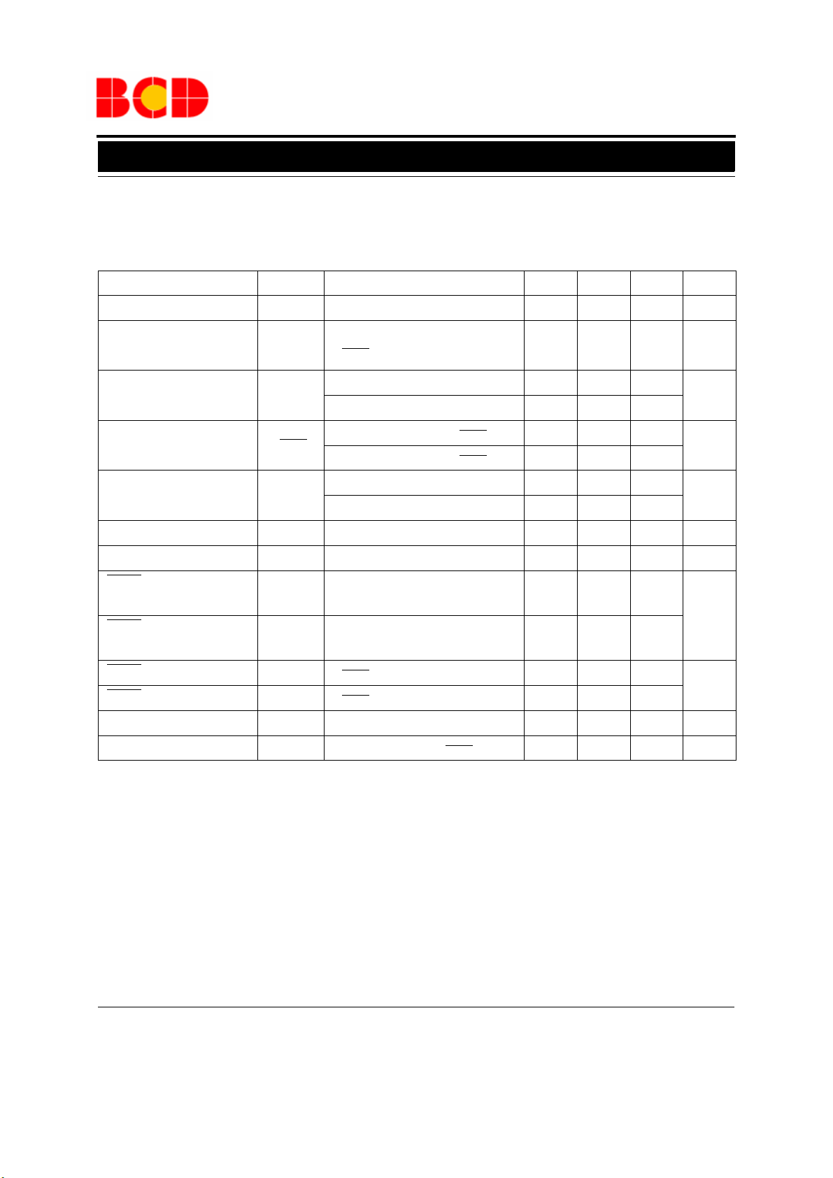
100mA REGULATED CHARGE PUMP AP3602A/B
Electrical Characteristics (Continued)
(C
FLY
=1μF, CIN=C
=10μF, TA=25
OUT
o
C, unless otherwise specified.)
For AP3602B
Parameter Symbol Conditions Min Typ Max Unit
Input Voltage V
Quiescent Current
Output Voltage
Shutdown Supply Current
Ripple Voltage
I
V
RIPPLE
Efficiency
Frequency f
SHDN
Input Threshold
High
SHDN
Input Threshold
Low
Input Current High I
SHDN
Input Current Low I
SHDN
V
Turn-on Time t
OUT
Short-Circuit Current I
IN
I
Q
V
O
SHDN
η
OSC
V
IH
V
IL
IH
IL
ON
SC
VO=4.5V 2.7 V
VIN=2.7V to 4.5V, IO=0mA,
=VIN, Not Switching
V
SHDN
13 30 μA
2.7V<VIN<4.5V, IO<50mA 4.32 4.5 4.68
3.0V<V
2.7V<VIN<3.6V, IO=0, V
3.6V<V
<4.5V, IO<100mA 4.32 4.5 4.68
IN
=0V 0.01 1
SHDN
<4.5V, IO=0, V
IN
=0V 2.5
SHDN
VIN=2.7V, IO=50mA 25
O
V
V
μA
mV
VIN=3V, IO=100mA 30
VIN=2.7V, IO=50mA 83 %
Oscillator free running 1.2 MHz
1.4
V
0.3
V
=V
V
SHDN
SHDN
IN
=0V -1 1
VIN=3V, IO=0mA 0.2
VIN=3V, VO=GND, V
=3V 300 mA
SHDN
-1 1
μA
ms
PP
Dec. 2012 Rev. 2. 0 BCD Semiconductor Manufacturing Limited
6
Page 7

Data Sheet
100mA REGULATED CHARGE PUMP AP3602A/B
Application Information
Operating Principles
The AP3602A/B use a switched capacitor charge
pump to boost the input voltage to a regulated output
voltage. Regulation is achieved by sensing the chip
output voltage through an internal resistor divider network. Controlled by an internal comparator (refer to
the functional block diagram), the charge pump circuit
is enabled when the divided output voltage is below a
preset trip point .
The charge pump operates at 1.2MHz with 50% duty
cycle. Conversion consists of a two-phase operation. In
the first phase, switches S2 and S3 are opened and S1
and S4 are closed. During this time, C
the voltage on V
. During the second phase, S2 and S3 are closed,
C
OUT
and load current is supplied by
IN
and S1 and S4 are opened. This action connects C
low side to VIN, C
age about 2*V
IN
high side to V
FLY
is used to charge C
OUT
load current. For each cycle, charges is transported
from V
IN
to V
to maintain the output voltage in its
OUT
nominal value.
This process breaks when the V
is high enough for
OUT
the reason of higher input voltage or lower load, then
the divided voltage at the control comparator exceeds
the internal trip point high level, which compels the
charge pump circuit enter to the idle mode in which the
switching cycle stops (pulse skipping) and the output
voltage is continually decreased because it is maintained by the discharging of C
only. In idle mode,
OUT
the feedback circuit continues sensing V
charges to
FLY
, then a volt-
OUT
and supply the
. If the
OUT
FLY
divided voltage at the control comparator drops below
the preset trip point, the comparator will start the
switching cycle again.
In idle mode, the AP3602A/B's quiescent current is
about 13
μA. In shutdown mode, all internal circuitry is
turned off and the AP3602A/B draw only leakage current from V
, which is less than 1μA. So, the shut-
IN
down power loss for AP3602A/B is very low, that is
beneficial to the battery supplied systems.
Short Circuit and Thermal Protection
The AP3602A/B have a thermal protection and shutdown circuit that continuously monitors the IC junction temperature.
When output short circuit occurs, the short circuit current is about 300mA (Typical). Under this condition,
the I
is about 2*Iout, which causes about 1.8W
IN
instant power dissipation on AP3602A/B, that will
cause a rise in the internal IC junction temperature. If
the thermal protection circuit senses the junction tem-
o
perature exceeding approximately 160
shutdown circuit will disable the charge pump switch-
ing circuit. The thermal hysteresis is about 10
means that the charge pump circuit can be active when
the short circuit is removed and the junction tempera-
ture drops below 150
o
C.
The thermal shutdown protection will cycle on and off
if an output short circuit condition persists. This will
allow the AP3602A/B to operate on a short circuit condition without latch up or damage to the device.
C, the thermal
o
C, which
Dec. 2012 Rev. 2. 0 BCD Semiconductor Manufacturing Limited
7
Page 8

Data Sheet
0 25 50 75 100 125 150
4.0
4.2
4.4
4.6
4.8
5.0
5.2
Output Voltage (V)
Output Current (mA)
AP3602-5.0V, VIN=3.0V
AP3602-5.0V, VIN=2.7V
2.5 3.0 3.5 4.0 4.5 5.0
40
50
60
70
80
90
100
Efficiency (%)
Input Voltage (V)
AP3602-5.0V, I
OUT
=25mA
AP3602-5.0V, I
OUT
=50mA
AP3602-5.0V, I
OUT
=100mA
0.1 1 10 100
70.0
72.5
75.0
77.5
80.0
82.5
85.0
87.5
90.0
92.5
95.0
Efficiency (%)
Output Current (mA)
AP3602-5.0V, VIN=2.7V
AP3602-5.0V, VIN=3.0V
V
SHDN
0V to 3V
100mA REGULATED CHARGE PUMP AP3602A/B
Typical Performance Characteristics
Typical Performance Characteristics for AP3602A
(Unless otherwise noted, V
=3.0V, CIN=C
IN
OUT
=10μF, C
=1μF Ceramic Cap, TA=25
FLY
o
C)
Figure 4. Output Voltage vs. Output Current
Figure 6. Efficiency vs. Output Current Figure 7. V
Dec. 2012 Rev. 2. 0 BCD Semiconductor Manufacturing Limited
Figure 5. Efficiency vs. Input Voltage
SHDN
2V/div
V
OUT
V
1V/div
Time 40μS/div
Start UpTime, @ No Load
OUT
8
Page 9

Data Sheet
V
SHDN
0V to 3V
V
SHDN
0V to 3V
I
OUT
0mA to 50mA
I
OUT
0mA to 100mA
100mA REGULATED CHARGE PUMP AP3602A/B
Typical Performance Characteristics (Continued)
Typical Performance Characteristics for AP3602A (Continued)
(Unless otherwise noted, V
=3.0V, CIN=C
IN
OUT
=10μF, C
=1μF Ceramic Cap, TA=25
FLY
o
C)
SHDN
2V/div
V
OUT
V
1V/div
Figure 8. V
OUT
I
50mA/div
Time 40μS/div
Start Up Time, @ 50mA Load
OUT
SHDN
2V/div
V
OUT
V
1V/div
Figure 9. V
OUT
I
50mA/div
Time 40μS/div
Start Up Time, @ 100mA Load
OUT
OUT
V
50mV/div
Time 200μS/div Time 200μS/div
Figure 10. Load Transient Response
OUT
V
50mV/div
Figure 11. Load Transient Response
Dec. 2012 Rev. 2. 0 BCD Semiconductor Manufacturing Limited
9
Page 10

Data Sheet
100mA REGULATED CHARGE PUMP AP3602A/B
Typical Performance Characteristics (Continued)
Typical Performance Characteristics for AP3602A (Continued)
(Unless otherwise noted, V
=3.0V, CIN=C
IN
OUT
=10μF, C
=1μF Ceramic Cap, TA=25
FLY
o
C)
10mV/div
Output Ripple
Time 2mS/div
Figure 12. Output Ripple @ VIN=2.7V, I
10mV/div
Output Ripple
OUT
=0mA
10mV/div
Output Ripple
Time 400nS/div
Figure 13. Output Ripple @ VIN=2.7V, I
OUT
=50mA
Time 400nS/div
Figure 14. Output Ripple @ VIN=2.7V, I
OUT
=100mA
Dec. 2012 Rev. 2. 0 BCD Semiconductor Manufacturing Limited
10
Page 11

Data Sheet
0 25 50 75 100 125 150
3.6
3.8
4.0
4.2
4.4
4.6
Output Voltage (V)
Output Current (mA)
AP3602-4.5V, VIN=3.0V
AP3602-4.5V, VIN=2.7V
0.1 1 10 100
60.0
62.5
65.0
67.5
70.0
72.5
75.0
77.5
80.0
82.5
85.0
Efficiency (%)
Output Current (mA)
AP3602-4.5V, VIN=2.7V
AP3602-4.5V, VIN=3.0V
2.53.03.54.04.5
40
50
60
70
80
90
Efficiency (%)
Input Voltage (V)
AP3602-4.5V, I
OUT
=25mA
AP3602-4.5V, I
OUT
=50mA
AP3602-4.5V, I
OUT
=100mA
I
OUT
0mA to 50mA
100mA REGULATED CHARGE PUMP AP3602A/B
Typical Performance Characteristics (Continued)
Typical Performance Characteristics for AP3602B
(Unless otherwise noted, V
=3.0V, CIN=C
IN
OUT
=10μF, C
=1μF Ceramic Cap, TA=25
FLY
o
C)
Figure 15. Output Voltage vs. Output Current
Figure 17. Efficiency vs. Output Current
Dec. 2012 Rev. 2. 0 BCD Semiconductor Manufacturing Limited
11
OUT
I
50mA/div
OUT
V
Figure 16. Efficiency vs. Input Voltage
50mV/div
Time 200μS/div
Figure 18. Load Transient Response
Page 12

Data Sheet
I
OUT
0mA to 100mA
100mA REGULATED CHARGE PUMP AP3602A/B
Typical Performance Characteristics (Continued)
Typical Performance Characteristics for AP3602B (Continued)
(Unless otherwise noted, V
OUT
I
50mA/div
OUT
V
50mV/div
=3.0V, CIN=C
IN
OUT
=10μF, C
Output Ripple
=1μF Ceramic Cap, TA=25
FLY
10mV/div
o
C)
Time 200μS/div
Figure 19. Load Transient Response
10mV/div
Output Ripple
Time 1μS/div
Figure 21. Output Ripple @ VIN=2.7V, I
OUT
=50mA
Time 40mS/div
Figure 20. Output Ripple @ VIN=2.7V, I
10mV/div
Output Ripple
Time 400nS/div
Figure 22. Output Ripple @ V
=2.7V, I
IN
OUT
OUT
=0mA
=100mA
Dec. 2012 Rev. 2. 0 BCD Semiconductor Manufacturing Limited
12
Page 13

Data Sheet
2.53.03.54.04.55.0
1000
1100
1200
1300
1400
1500
1600
1700
1800
Frequency (kHz)
Supply Voltage (V)
TA=-50oC
TA=25oC
TA=100oC
-50-250 255075100
-1.00
-0.75
-0.50
-0.25
0.00
0.25
0.50
0.75
1.00
Normalized Output Voltage (%)
Temperature (oC)
VIN=3.0V, I
OUT
=25mA
012345
0
4
8
12
16
20
Supply Current (μA)
SHDN Voltage (V)
VIN=2.7V
VIN=3.0V
2.53.03.54.04.55.0
10
12
14
16
18
20
Supply Current (μA)
Supply Voltage (V)
No Load, Not Switching
100mA REGULATED CHARGE PUMP AP3602A/B
Typical Performance Characteristics (Continued)
Typical Performance Characteristics for AP3602A/B
(Unless otherwise noted, V
=3.0V, CIN=C
IN
OUT
=10μF, C
=1μF Ceramic Cap, TA=25
FLY
o
C)
Figure 23. Supply Current vs. Supply Voltage
Figure 25. Oscillator Frequency vs. Supply Voltage
Dec. 2012 Rev. 2. 0 BCD Semiconductor Manufacturing Limited
Figure 24. Supply Current vs. SHDN
Voltage
Figure 26. Normalized Output Voltage vs. Temperature
13
Page 14

Data Sheet
2.53.03.54.04.55.0
0.5
0.6
0.7
0.8
0.9
1.0
SHDN Input Threshold High Voltage (V)
Input Voltage (V)
TA=-40oC
TA=25oC
TA=85oC
2.53.03.54.04.55.0
0.5
0.6
0.7
0.8
0.9
1.0
SHDN Input Threshold Low Voltage (V)
Input Voltage (V)
TA=-40oC
TA=25oC
TA=85oC
100mA REGULATED CHARGE PUMP AP3602A/B
Typical Performance Characteristics (Continued)
Typical Performance Characteristics for AP3602A/B (Continued)
(Unless otherwise noted, V
=3.0V, CIN=C
IN
OUT
=10μF, C
=1μF Ceramic Cap, TA=25
FLY
o
C)
Figure 27. VIH vs. VIN Figure 28. VIL vs. VIN
Dec. 2012 Rev. 2. 0 BCD Semiconductor Manufacturing Limited
14
Page 15

Data Sheet
VIN=2.7V to 4.2V
10μF
1μF
V
IN
V
OUT
GND
SHDN
AP3602A
C+ C-
10μF
4 * 120Ω
LED's VF=3.2V
VIN=2.7V to 4.2V
10μF
1μF
V
IN
V
OUT
GND
SHDN
AP3602B
C+ C-
4 * 91Ω
LED's VF=3.2V
10μF
100mA REGULATED CHARGE PUMP AP3602A/B
Typical Application
Figure 29. AP3602A Typical Application Circuit
Figure 30. AP3602B Typical Application Circuit
Dec. 2012 Rev. 2. 0 BCD Semiconductor Manufacturing Limited
15
Page 16

Data Sheet
2.820(0.111)
3.020(0.119)
2.650(0.104)
2.950(0.116)
1.500(0.059)
1.700(0.067)
0.950(0.037)TYP
1.800(0.071)
2.000(0.079)
0.300(0.012)
0.400(0.016)
0.700(0.028)REF
0.100(0.004)
0.200(0.008)
0°
8°
0.200(0.008)
0.300(0.012)
0.600(0.024)
0.000(0.000)
0.150(0.006)
0.900(0.035)
1.300(0.051)
1.450(0.057)
MAX
123
4
5
6
Pin 1 Mark
100mA REGULATED CHARGE PUMP AP3602A/B
Mechanical Dimensions
SOT-23-6
Unit: mm(inch)
Dec. 2012 Rev. 2. 0 BCD Semiconductor Manufacturing Limited
16
Page 17

BCD Semiconductor Manufacturing Limited
IMPORTANT NOTICE
IMPORTANT NOTICE
BCD Semiconductor Manufacturing Limited reserves the right to make changes without further notice to any products or specifi-
BCD Semiconductor Manufacturing Limited reserves the right to make changes without further notice to any products or specifi-
cations herein. BCD Semiconductor Manufacturing Limited does not assume any responsibility for use of any its products for any
cations herein. BCD Semiconductor Manufacturing Limited does not assume any responsibility for use of any its products for any
particular purpose, nor does BCD Semiconductor Manufacturing Limited assume any liability arising out of the application or use
particular purpose, nor does BCD Semiconductor Manufacturing Limited assume any liability arising out of the application or use
of any its products or circuits. BCD Semiconductor Manufacturing Limited does not convey any license under its patent rights or
of any its products or circuits. BCD Semiconductor Manufacturing Limited does not convey any license under its patent rights or
other rights nor the rights of others.
other rights nor the rights of others.
http://www.bcdsemi.com
MAIN SITE
MAIN SITE
- Headquarters
BCD Semiconductor Manufacturing Limited
BCD Semiconductor Manufactur ing Limited
- Wafer Fab
No. 1600, Zi Xing Road, Shanghai ZiZhu Science-based Industrial Park, 200241, China
Shanghai SIM-BCD Semiconductor Manufacturing Limited
Tel: +86-21-24162266, Fax: +86-21-24162277
800, Yi Shan Road, Shanghai 200233, China
Tel: +86-21-6485 1491, Fax: +86-21-5450 0008
REGIONAL SALES OFFICE
Shenzhen Office
REGIONAL SALES OFFICE
Shanghai SIM-BCD Semiconductor Manufacturing Co., Ltd., Shenzhen Office
Shenzhen Office
Unit A Room 1203, Skyworth Bldg., Gaoxin Ave.1.S., Nanshan District, Shenzhen,
Shanghai SIM-BCD Semiconductor Manufacturing Co., Ltd. Shenzhen Office
China
Advanced Analog Circuits (Shanghai) Corporation Shenzhen Office
Tel: +86-755-8826 7951
Room E, 5F, Noble Center, No.1006, 3rd Fuzhong Road, Futian District, Shenzhen 518026, China
Fax: +86-755-8826 7865
Tel: +86-755-8826 7951
Fax: +86-755-8826 7865
- Wafer Fab
BCD Semiconductor Manufacturing Limited
Shanghai SIM-BCD Semiconductor Manufacturing Co., Ltd.
- IC Design Group
800 Yi Shan Road, Shanghai 200233, China
Advanced Analog Circuits (Shanghai) Corporation
Tel: +86-21-6485 1491, Fax: +86-21-5450 0008
8F, Zone B, 900, Yi Shan Road, Shanghai 200233, China
Tel: +86-21-6495 9539, Fax: +86-21-6485 9673
Taiwan Office
BCD Semiconductor (Taiwan) Company Limited
Taiwan Office
4F, 298-1, Rui Guang Road, Nei-Hu District, Taipei,
BCD Semiconductor (Taiwan) Company Limited
Tai wan
4F, 298-1, Rui Guang Road, Nei-Hu District, Taipei,
Tel: +886-2-2656 2808
Taiwan
Fax: +886-2-2656 2806
Tel: +886-2-2656 2808
Fax: +886-2-2656 2806
USA Office
BCD Semiconductor Corp.
USA Office
30920 Huntwood Ave. Hayward,
BCD Semiconductor Corporation
CA 94544, USA
30920 Huntwood Ave. Hayward,
Tel : +1-510-324-2988
CA 94544, U.S.A
Fax: +1-510-324-2788
Tel : +1-510-324-2988
Fax: +1-510-324-2788
 Loading...