

Page 1
AP3595
Document number: DS36749 Rev. 1 - 2
1 of 23
www.diodes.com
January 2014
© Diodes Incorporated
AP3595
A Product Line of
Diodes Incorporated
Description
The AP3595 is a compact dual phase synchronous rectified buck
controller specifically designed to deliver high quality output voltage.
This device operates at adjustable operation frequency and is
capable of delivering up to 60A output current.
This controller integrates internal MOSFET drivers that support
12V+12V bootstrapped voltage for high efficiency power conversion.
The bootstrap diode is built-in to simplify the circuit design and
minimize external part count.
The AP3595 features configurable gate driving voltage for maximum
efficiency and optimal performance. The built-in bootstrap diode
simplifies the circuit design and reduces external part count and PCB
space. The output voltage is precisely regulated to the reference input
that is dynamically adjustable by external voltage divider.
Other features include adjustable soft start, adjustable operation
frequency, and quick response to step-load transient. With aforementioned functions, the IC provides customers a compact, high
efficiency, well-protected and cost-effective solution.
This IC is available in U-QFN4040-24 package.
Features
Operate with Single Supply Voltage
Simple Single Loop Voltage Mode Control
12V+12V Bootstrapped Drivers with Internal Bootstrap Diode
Adjustable Over Current Protection by DCR
Current Sensing
Adjustable Current Balancing by R
DS(ON)
Current Sensing
Adjustable Operation Frequency from 50kHz to 1MHz Per Phase
External Compensation
Dynamic Output Voltage Adjustment
Adjustable Soft Start
U-QFN4040-24 Package
RoHS Compliant and 100% Lead (Pb)-free
Totally Lead-free & Fully RoHS Compliant (Note1 & 2)
Halogen and Antimony Free. “Green” Device (Note 3)
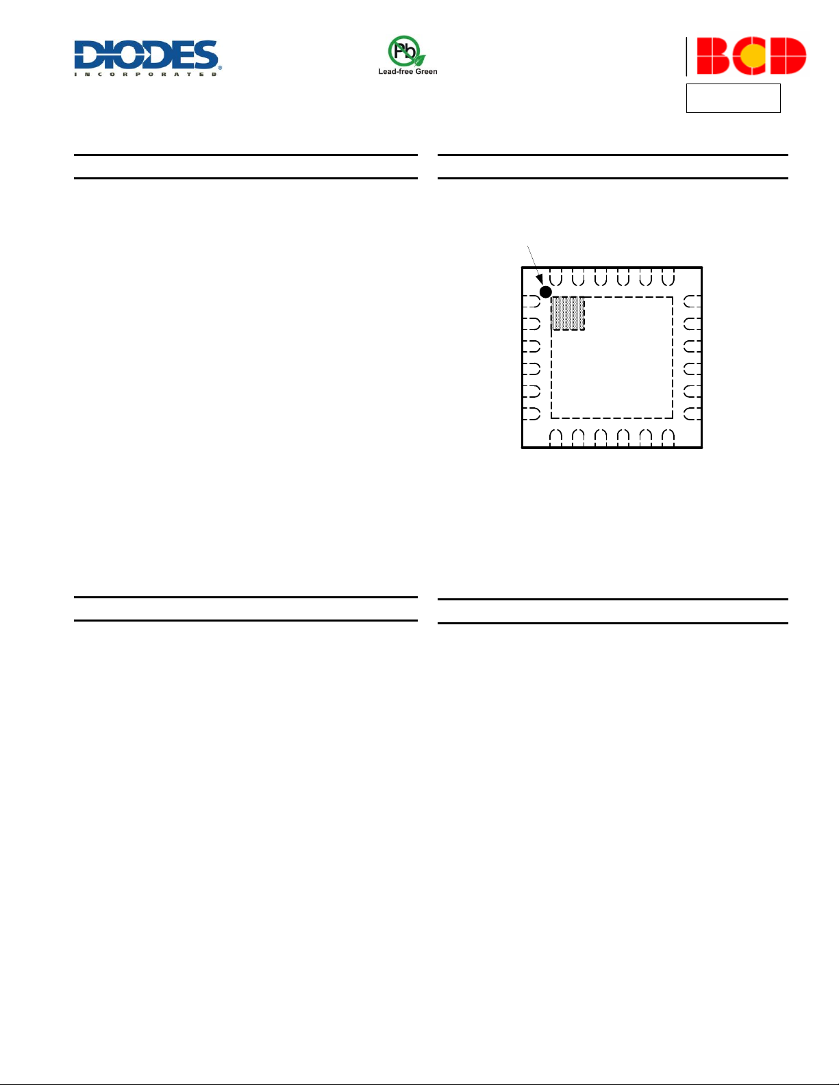
Pin Assignments
(Top View)
LG2
PHASE2
HG2
BOOT2
VID
RSET
PSI
CSP
CSN
SS
EAP
FBRTN
FB
COMP
IOFS
RT/EN
VREF
REFIN
VCC
PVCC
LG1
PHASE1
HG1
BOOT1
Pin 1 Mark
EP
1
10
2
3
4
5
6
7 8 9 11 12
13
14
15
16
17
18
192021222324
U-QFN4040-24 (FN Package)
Applications
Middle-High End GPU Core Power
High End Desktop PC Memory Core Power
Low Output Voltage, High Power Density
DC-DC Converters
Voltage Regulator Modules
Notes: 1. No purposely added lead. Fully EU Directive 2002/95/EC (RoHS) & 2011/65/EU (RoHS 2) compliant.
2. See http://www.diodes.com/quality/lead_free.html for more information about Diodes Incorporated’s definitions of Halogen- and Antimony-free, "Green"
and Lead-free.
3. Halogen- and Antimony-free "Green” products are defined as those which contain <900ppm bromine, <900ppm chlorine (<1500ppm total Br + Cl) and
<1000ppm antimony compounds.
DUAL PHASE SYNCHRONOUS RECTIFIED BUCK CONTROLLER
Page 2
AP3595
Document number: DS36749 Rev. 1 - 2
2 of 23
www.diodes.com
January 2014
© Diodes Incorporated
AP3595
A Product Line of
Diodes Incorporated
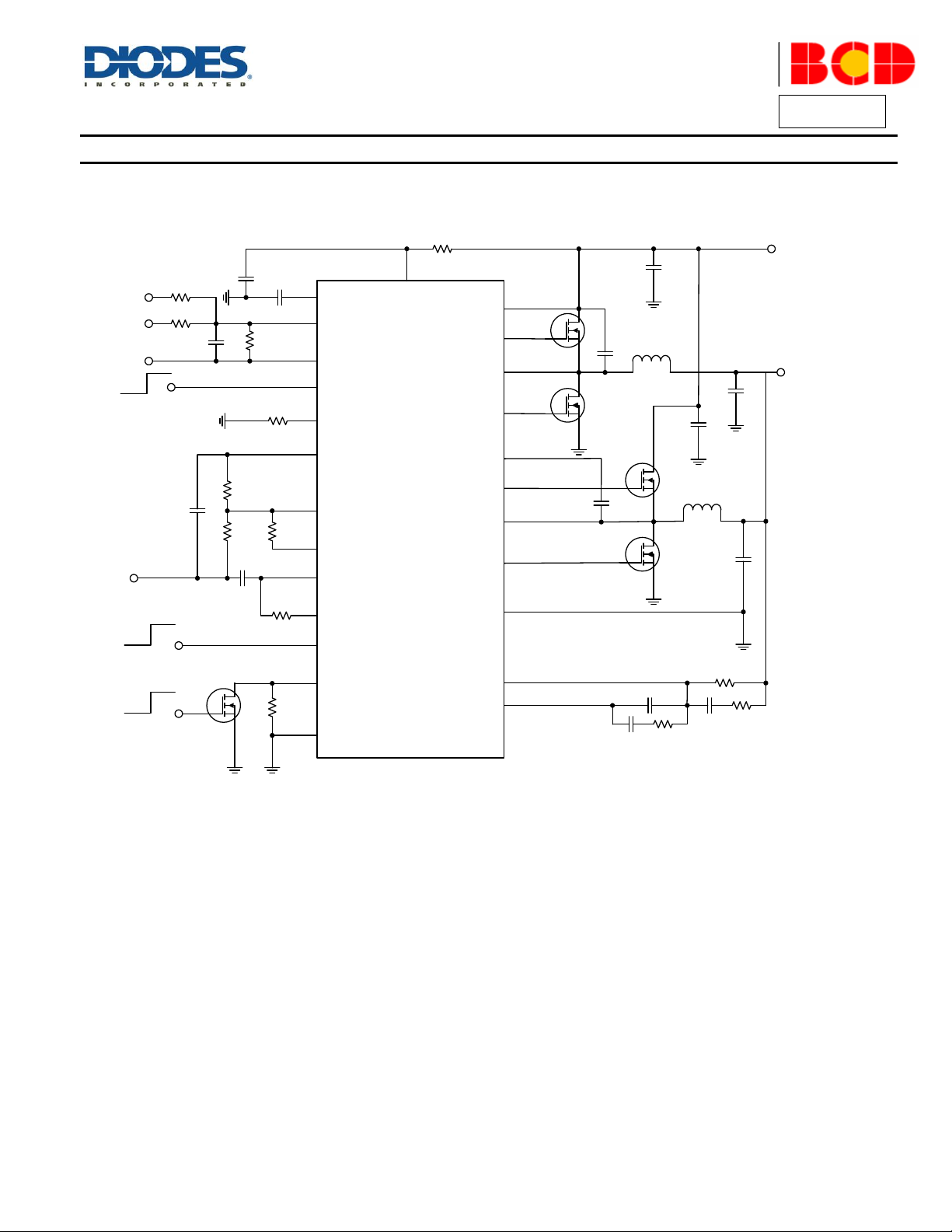
AP3595
BOOT1
HG1
PHASE1
LG1
VCC
V
OUT
V
IN
BOOT2
HG2
PHASE2
LG2
FBRTN
FB
COMP
RT/EN
GND
VID
EAP
RSET
SS
REFIN
VREF
IOFS
PSI
PVCC
CSP
FBRTN
CSN
PHASE2
PHASE1
V
OUT
17
11
10
12
4
2
1
24
9
8
23
3
5
6
7
19
20
21
22
16
15
14
13
18
Typical Applications Circuit
Page 3
AP3595
Document number: DS36749 Rev. 1 - 2
3 of 23
www.diodes.com
January 2014
© Diodes Incorporated
AP3595
A Product Line of
Diodes Incorporated
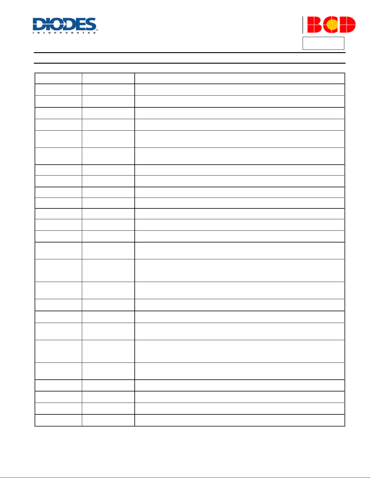
Pin Number
Pin Name
Function
1
REFIN
External Reference Input. This is the input pin of external reference voltage. Connect a voltage
divider from VREF to REFIN and FBRTN to set the reference voltage
2
VREF
Output for Reference Voltage. This is the output pin of high precision 2V reference voltage.
Bypass this pin with a 1F ceramic capacitor to FBRTN
3
RT/EN
Operation Frequency Setting. Connecting a resistor between this pin and GND to set the
operation frequency. Pull this pin to ground to shut down the AP3595
4
IOFS
Current Balance Adjustment. Connect a resistor from this pin to VREF or GND to adjust the
current sharing
5
COMP
Error Amplifier Output. This is the output of the error amplifier (EA) and the non-inverting input
of the PWM comparators. Use this pin in combination with the FB pin to compensate the
voltage control feedback loop of the converter
6
FB
Feedback Voltage. This pin is the inverting input to the error amplifier. Use this pin in
combination with the COMP pin to compensate the voltage control feedback loop of the
converter
7
FBRTN
Feedback Return. Connect this pin to the ground where the output voltage is to be regulated
8
EAP
Non-inverting Input of Error Amplifier. Connect a resistor from this pin to SS pin to set the
droop slope
9
SS
Soft Start Output. Connect a capacitor to FBRTN to set the soft start interval
10
CSN
Negative Input for Current Sensing Amplifier
11
CSP
Positive Input for Current Sensing Amplifier
12
PSI
Power Saving Mode. Connect this pin to VREF for always two phase operation. Short this pin
to ground for always single phase operation
13
BOOT1
Bootstrap Supply for the Floating Upper Gate Driver of Channel 1. Connect a bootstrap
capacitor between BOOT1 pin and the PHASE1 pin to form a bootstrap circuit
14
HG1
Upper Gate Driver Output for Channel 1. Connect this pin to the gate of upper MOSFET. This
pin is monitored by the adaptive shoot-through protection circuitry to determine when the upper
MOSFET has turned off
15
PHASE1
Switch Node for Channel 1. Connect this pin to the source of the upper MOSFET and the drain
of the lower MOSFET. This pin is used as the sink for the Upper GATE driver. It is also
monitored by the adaptive shoot-through protection circuitry to determine when the upper
MOSFET has turned off
16
LG1
Lower Gate Driver Output for Channel 1. Connect this pin to the gate of lower MOSFET. This
pin is monitored by the adaptive shoot-through protection circuitry to determine when the lower
MOSFET has turned off
17
PVCC
Supply Voltage for Gate Driver. This pin is the output of internal 9V LDO. This pin provides
current for gate drivers. Bypass this pin with a minimum 1F ceramic capacitor
18
VCC
Supply Voltage. This pin provides current for internal control circuit and 9V LDO. Bypass this
pin with a minimum 1F ceramic capacitor next to the IC
19
LG2
Lower Gate Driver Output for Channel 2. Connect this pin to the gate of lower MOSFET. This
pin is monitored by the adaptive shoot-through protection circuitry to determine when the lower
MOSFET has turned off
20
PHASE2
Switch Node for Channel 2. Connect this pin to the source of the upper MOSFET and the drain
of the lower MOSFET. This pin is used as the sink for the HG2 driver. It is also monitored by
the adaptive shoot-through protection circuitry to determine when the upper MOSFET has
turned off
21
HG2
Upper Gate Driver Output for Channel 2. Connect this pin to the gate of upper MOSFET. This
pin is monitored by the adaptive shoot-through protection circuitry to determine when the upper
MOSFET has turned off
22
BOOT2
Bootstrap Supply for the Floating Upper Gate Driver of Channel 2. Connect a bootstrap
capacitor between BOOT2 pin and the PHASE2 pin to form a bootstrap circuit
23
VID
VID Input. This pin is used to adjust the reference voltage. Logic high enables the internal
MOSFET connected to RSET pin
24
RSET
Reference Voltage Setting. This pin is an open drain output that is pulled low when VID sets to
high. Connect a resistor from this pin to REFIN pin to set the reference voltage
Exposed Pad
GND
Power Ground. Tie this pin to the ground island/plane through the lowest available impedance
connection
Pin Descriptions
Page 4
AP3595
Document number: DS36749 Rev. 1 - 2
4 of 23
www.diodes.com
January 2014
© Diodes Incorporated
AP3595
A Product Line of
Diodes Incorporated
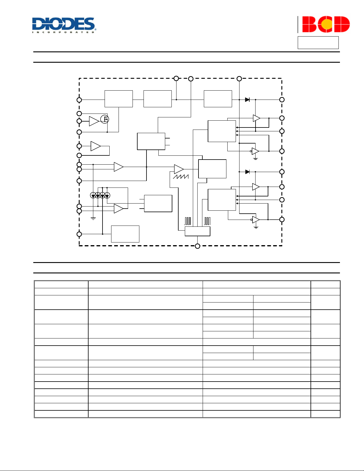
Reference
Voltage
POR
Internal
Regulator
Gate
Control
Logic
DUAL PHASE
Control
Gate
Control
Logic
OCP
OVP
UVP
Power Saving
Setting
Oscillator
+
-
BOOT1
HG1
PHASE1
LG1
BOOT2
HG2
LG2
PVCC
+
-
PWM
Current
Balance
RT/EN
PHASE1
PHASE2
IOFS
VREF
RSET
VID
FBRTN
REFIN
SS
EAP
FB
Error
Amplifier
COMP
+
-
CSN
CSP
PSI
FB
SS
VCC
2
24
23
1
9
8
6
5
10
11
12
3
19
20
15
21
22
16
14
13
17
4
18
PHASE2
7
Symbol
Parameter
Rating
Unit
VCC
Supply Input Voltage
-0.3 to 15
V
V
PHASE
PHASE to GND Voltage
DC
-0.3 to 15
V
<200ns
-5 to 30
VHG
HG to PHASE Voltage
DC
-0.3 to V
BOOT-PHASE
+0.3
V
<200ns
-5 to V
BOOT-PHASE
+5
VLG
LG to GND Voltage
DC
-0.3 to VCC+0.3
V
<200ns
-5 to VCC+5
–
BOOT to PHASE Voltage
15
V
V
BOOT
BOOT to GND Voltage
DC
-0.3 to V
PHASE
+15
V
<200ns
-0.3 to 42
Input, Output or I/O Voltage
-0.3 to 6
V
PD
Power Dissipation
2.5
W
JA
Thermal Resistance (Junction to Ambient)
40
°C/W
T
STG
Storage Temperature Range
-65 to +150
ºC
TJ
Junction Temperature
+150
ºC
T
LEAD
Lead Temperature (Soldering, 10sec)
+260
ºC
V
HBM
ESD (Human Body Model)
2000
V
V
MM
ESD (Machine Model)
200
V
Functional Block Diagram
Absolute Maximum Ratings(Note 4)
Note 4: Stresses greater than those listed under “Absolute Maximum Ratings” may cause permanent damage to the device. These are stress ratings only, and
functional operation of the device at these or any other conditions beyond those indicated under “Recommended Operating Conditions” is not implied.
Exposure to “Absolute Maximum Ratings” for extended periods may affect device reliability.
Page 5
AP3595
Document number: DS36749 Rev. 1 - 2
5 of 23
www.diodes.com
January 2014
© Diodes Incorporated
AP3595
A Product Line of
Diodes Incorporated
Symbol
Parameter
Min
Max
Unit
VCC
Supply Input Voltage
10.8
13.2
V
TA
Operating Ambient Temperature
-40
+85
°C
TJ
Operating Junction Temperature
-40
+125
°C
Symbol
Parameter
Conditions
Min
Typ
Max
Unit
SUPPLY INPUT
VCC
Supply Input Voltage
–
10.8
–
13.2
V
ICC
Supply Current
HG and LG Open, VCC=12V,
Switching
– 5 –
mA
IQ
Quiescent Current
No Switching, I
PCC
=0mA
– 4 –
mA
V
PCC
Regulated Supply Voltage
RT/EN=0V, I
PCC
=0mA
8 9 10
V
V
RTH
POR Threshold
–
8 9 10
V
V
HYS
POR Hysteresis
–
– 1 –
V
CHIP ENABLE/FREQUENCY SETTING
I
RT/EN
RT/EN Sourcing Current
V
RT/EN
=GND
100
150
200
A
V
RT/EN
RT/EN Voltage
RRT=33kΩ
– 1 – V –
Switching Frequency Setting Range
–
50 – 1000
kHz
f
OSC
Free Run Switching Frequency
RRT=33kΩ
270
300
330
kHz
△f
OSC
Switching Frequency Accuracy
f
OSC
=200kHz to 500kHz
-15 – 15
%
OSCILLATOR
–
Maximum Duty Cycle
–
–
40 – %
–
Minimum Duty Cycle
–
– 0 –
%
V
OSC
Ramp Amplitude
VCC=12V
–
3.5 – V
POWER SAVING MODE
V
PSI_H
Threshold Voltage for Entering Dual
Phase
V
PSI
rising
1.2 – –
V
V
PSI_L
Threshold Voltage for Entering
Single Phase
V
PSI
falling
– – 0.4
V
REFERENCE VOLTAGE
V
REF
Reference Voltage Accuracy
I
REF
=100A
1.98
2.0
2.02
V
△V
REF
Reference Voltage Load Regulation
I
REF
=0 to 2mA
-5 – 5
mV
△V
FB
Output Voltage Accuracy
|V
REFIN-VFB
|, VCC=12V, No Load,
R
DRP
=0, V
REFIN
=0.8V to 1.6V
– – 5
mV
ERROR AMPLIFIER
AO
Open Loop DC Gain
Guaranteed by design
70
80 – dB
GBW
Gain Bandwidth Product
C
LOAD
=5pF, Guaranteed by design
–
20 – MHz
SR
Slew Rate
Guaranteed by design
15
20
–
V/s
I
COMP
Maximum Current (Sink and Source)
V
COMP
=1.6V
1.5
2.0 – mA
Recommended Operating Conditions
Electrical Characteristics (@V
=12V, TA=+25C, unless otherwise specified.)
CC
Page 6
AP3595
Document number: DS36749 Rev. 1 - 2
6 of 23
www.diodes.com
January 2014
© Diodes Incorporated
AP3595
A Product Line of
Diodes Incorporated
Symbol
Parameter
Conditions
Min
Typ
Max
Unit
SOFT START
ISS
Soft Start Current
During soft start
–
22
–
A
I
SS_CC
Supply Current
After soft start end
–
200
–
A
TOTAL CURRENT SENSE
I
CSN_MAX
Maximum Sourcing Current
–
100 – –
A
–
GM Amplifier Offset Voltage
–
-5 0 5
mV
I
CSN_OCP
Over Current Protection Threshold
–
–
60
–
A
I
DRP/ICSN
Droop Accuracy
–
90
100
110
%
I
PSI/ICSN
PSI Accuracy
–
90
100
110
%
PHASE CURRENT SENSE
–
Trans-conductance
–
–
1.0 – mS
V
OFS
IOFS Voltage
100kfrom IOFS to VREF
–
1.5
–
V
100kfrom IOFS to GND
–
0.5
–
VID CONTROL INPUT
VIH
Logic High Threshold Level
–
1.2 – –
V
VIL
Logic Low Threshold Level
–
– – 0.4
V
R
RSET
On Resistance of RSET MOSFET
VID=High
–
20
–
I
RSET
Leakage Current of RSET Pin
V
RSET
=2V, VID=0V
– – 0.1
A
GATE DRIVER
I
HG_SRC
Upper Gate Sourcing Current
V
BOOT-VPHASE
=6V
–
1.2 – A
R
HG_SNK
Upper Gate Sinking Resistance
IHG=100mA sinking
–
1.5
3
I
LG_SRC
Lower Gate Sourcing Current
V
PCC-VLG
=6V
–
1.2 – A
R
LG_SNK
Lower Gate Sinking Resistance
ILG=100mA sinking
– 1 2
tDT
Dead Time
–
–
50 – ns
PROTECTION
VFB-VSS
Over Voltage Protection
–
–
300 – mV
VFB-VSS
Under Voltage Protection
–
–
-300
–
mV
–
Over Temperature Protection
–
–
+150
–
°C
–
Over Temperature Hysteresis
–
–
+20 – °C
Electrical Characteristics (Cont.) (@V
=12V, TA=+25C, unless otherwise specified.)
CC
Page 7
AP3595
Document number: DS36749 Rev. 1 - 2
7 of 23
www.diodes.com
January 2014
© Diodes Incorporated
AP3595
A Product Line of
Diodes Incorporated
4 6 8 10 12 14
1.980
1.982
1.984
1.986
1.988
1.990
1.992
1.994
1.996
1.998
2.000
V
REF
(V)
VCC (V)
I
LOAD
=0mA
I
LOAD
=2mA
0 5 10 15 20
1.980
1.982
1.984
1.986
1.988
1.990
1.992
1.994
1.996
1.998
2.000
V
REF
(V)
I
LOAD
(mA)
0 20 40 60 80 100
8.85
8.90
8.95
9.00
9.05
9.10
V
PCC
(V)
I
LOAD
(mA)
4 6 8 10 12 14
3
4
5
6
7
8
9
V
PCC
(V)
VIN (V)
I
LOAD
=0mA
I
LOAD
=10mA
9 10 11 12 13 14
4.6
4.8
5.0
5.2
5.4
5.6
5.8
6.0
6.2
6.4
I
CC
(mA)
VIN (V)
9 10 11 12 13 14
290
292
294
296
298
300
302
304
306
308
310
f
OSC
(kHz)
VIN (V)
Performance Characteristics
V
V
Line Regulation V
REF
Load Regulation V
PCC
ICC vs.V
IN
f
Load Regulation
REF
Line Regulation
PCC
vs.V
OSC
IN
Page 8

AP3595
Document number: DS36749 Rev. 1 - 2
8 of 23
www.diodes.com
January 2014
© Diodes Incorporated
AP3595
A Product Line of
Diodes Incorporated
10 100
10
100
1000
f
OSC
(kHz)
RRT (k)
-40 -20 0 20 40 60 80 100 120 140
8.96
8.98
9.00
9.02
9.04
9.06
9.08
9.10
V
PCC
(V)
Temperature (oC)
I
LOAD
=0mA
I
LOAD
=10mA
-40 -20 0 20 40 60 80 100 120 140
1.980
1.982
1.984
1.986
1.988
1.990
1.992
1.994
1.996
1.998
2.000
V
REF
(V)
Temperature (oC)
-40 -20 0 20 40 60 80 100 120 140
290
292
294
296
298
300
302
304
306
308
310
f
OSC
(kHz)
Temperature (oC)
Time 200s/div
V
PHASE1
10V/div
V
RT/EN
1V/div
V
OUT
1V/div
V
SS
1V/div
V
PHASE1
10V/div
V
RT/EN
1V/div
V
OUT
1V/div
V
SS
1V/div
Time 4ms/div
Performance Characteristics (Cont.)
f
OSC
vs. R
V
RT
V
vs. Temperature f
REF
Power On Waveforms Power Off Waveforms
vs. Temperature
PCC
vs. Temperature
OSC
Page 9

AP3595
Document number: DS36749 Rev. 1 - 2
9 of 23
www.diodes.com
January 2014
© Diodes Incorporated
AP3595
A Product Line of
Diodes Incorporated
Time 200s/div
V
PHASE1
10V/div
V
RT/EN
1V/div
V
OUT
1V/div
V
SS
500mV/div
V
PHASE1
10V/div
V
RT/EN
1V/div
V
OUT
1V/div
V
SS
500mV/div
Time 1ms/div
Time 40ns/div
V
HG
5V/div
V
PHASE
5V/div
V
LG
5V/div
V
HG
5V/div
V
LG
5V/div
Time 40ns/div
V
PHASE
5V/div
V
HG VLG
V
HG VLG
V
PHASE
V
PHASE
Time 2ms/div
V
PSI
2V/div
V
PHASE1
10V/div
V
PHASE2
10V/div
VFB
1V/div
V
HG1
5V/div
V
LG1
5V/div
Time 4s/div
Performance Characteristics (Cont.)
EN On Waveform EN Off Waveform
Dead Time 1 Dead Time 2
OVP Function PSI Function
Page 10

AP3595
Document number: DS36749 Rev. 1 - 2
10 of 23
www.diodes.com
January 2014
© Diodes Incorporated
AP3595
A Product Line of
Diodes Incorporated
V
ID
5V/div
Time 2ms/div
V
OUT
200mV/div
Performance Characteristics (Cont.)
VID Change
Application Information
1. Overview
AP3595 is a dual-phase synchronous-rectified buck controller designed to deliver high quality output voltage for high power applications. It is
capable of delivering up to 60A output current with embedded bootstrapped drivers that support 12V+12V driver capability. The built-in bootstrap
diode simplifies the circuit design and reduces external part count and PCB space.
The output voltage is precisely regulated to the reference input that is dynamically adjustable by external voltage divider. The adjustable current
balance is achieved by R
AP3595 features comprehensive protection functions including over current protection, input/output under voltage protection, over voltage
protection and over temperature protection.
Other features include adjustable soft start, adjustable operation frequency, and quick response to step load transient. With aforementioned
functions, the IC provides customer a compact, high efficiency, well-protected and cost effective solution.
2. Power on Reset
A Power On Reset (POR) circuitry continuously monitors the supply voltage at VCC. Once the rising POR threshold is exceeded, the AP3595 sets
itself to active state and is ready to accept chip enable command. The rising POR threshold is typically 9V.
3. Soft Start
The AP3595 initiates its soft start cycle when the RT/EN pin is released from ground once the POR is granted as shown in Figure 1.
current sensing technique.
DS(ON)
Figure 1. Soft Start Cycle (R
DRP
=0)
Page 11

AP3595
Document number: DS36749 Rev. 1 - 2
11 of 23
www.diodes.com
January 2014
© Diodes Incorporated
AP3595
A Product Line of
Diodes Incorporated
)(
)(
10000
kHz
kR
f
FS
OSC
A1210RII
3
)ON(DSLXCSX
SS
FBEAP
SS
C
A
dt
dV
dt
dV
dt
dV
22
SS
FBEAP
SS
C
A
dt
dV
dt
dV
dt
dV
200
R
FS
(k)
Sample
&Hold
Current
Balance
I
CS1
I
CS2
_
+
Reference
Voltage
+
_
PHASE
Application Information (Cont.)
As mentioned in the above section, the slew rate of voltage transition at SS pin and V
capacitor connected to the SS pin. This reduces inrush current to charge/discharge the large output capacitors during soft start and VID changing,
and prevents OCP, OVP/UVP false trigger. The SS buffer sinking/sourcing capability is limited to 22A during soft start and 200A after soft start
end. Therefore, the slew rate of voltage ramping up/down at SS, EAP and FB pin during soft start or VID changing is calculated as:
During Soft Start
After Soft Start
4. Pre-Bias Function
AP3595 features pre-bias start-up capability. If the output voltage is pre-biased with a voltage V
reference voltage ramping V
output low until the ramping V
. The error amplifier keeps V
EAP
catches up the feedback voltage. The IC keeps both upper and lower MOSFETs off until the first pulse takes
EAP
lower than the valley of the saw tooth waveform and makes PWM comparators
COMP
place.
5. Chip Oscillator Frequency Programming
A resistor RFS connected to RT/EN pin programs the oscillator frequency as:
during soft start and V
OUT
BIAS
jumping is controlled by the
REFIN
, that accordingly makes VFB higher than
Figure 2 shows the relationship between oscillation frequency and RFS.
Figure 2. Switching Frequency vs. R
When released, the RT/EN pin voltage is regulated at 1V. Pulling the RT/EN pin to ground shuts down the IC.
6. Current Balance
AP3595 extracts phase currents for current balance by parasitic on-resistance of the lower switches when turned on as shown in Figure 3.
The GM amplifier senses the voltage drop across the lower switch and converts it into current signal when it turns on. The sampled and held
current is expressed as:
Figure 3. R
Current Sensing Scheme
DS(ON)
FS
Page 12

AP3595
Document number: DS36749 Rev. 1 - 2
12 of 23
www.diodes.com
January 2014
© Diodes Incorporated
AP3595
A Product Line of
Diodes Incorporated
2/
DCOUTCS
RIV
CSCSPDC
CRRL /2
CSCSNCSN
VRI
CSN
DCOUT
CSN
R
RI
I
2
+
_
+
_
PWM1
PWM2
COMP
I
CS2
I
CS1
+
_
+
RAMP1
RAMP2
AP3595
+
-
CSP
CSN
R
CSN
R
CSP
C
CS
R
DC
R
DC
L
L
R
CSP
PHASE1
PHASE2
V
OUT
GM
Amplifier
I
CSN
I
DRPIPSIIOCP
Application Information (Cont.)
Where ILX is the phase x current in Ampere, R
offset voltage of the current sensing circuit.
AP3595 tunes the duty cycle of each channel for current balance according to the sensed inductor current signals as shown in Figure 4. If the
current of channel 1 is smaller than the current of channel 2, the IC increases the duty cycle of the corresponding phase to increase its phase
current accordingly, vice versa.
7. Power Saving Interface (PSI)
The AP3595 supports dual phase or single phase which is controlled by V
AP3595 will operate in single phase mode. There is 2ms delay at the transient from dual phase to single phase, and no delay time from single
phase to dual phase.
8. Current Sense by DCR
The above figure shows the output current sensing block of AP3595. The voltage VCS across the current sensing capacitor C
as
If the following condition is true:
Where L is the output inductor of the buck converter, RDC is the parasitic resistance of the inductor, R
current sensing.
The GM amplifier will source a current I
Therefore the output current signal I
The output current signal I
,
is used to droop tuning and output over current protection.
CSN
is the on-resistance of low side MOSFET, 12A is a constant current to compensate the
DS(ON)
Figure 4. Current Balance Scheme of AP3595
. If V
PSI
Figure 5. Output Current Sensing Block
to the CSN pin to let its inputs virtually short circuit.
CSN
can be expressed as:
CSN
>1.2V, AP3595 will operate in dual phase mode. If V
PSI
can be expressed
CS
and CCS are the external RC network for
CSP
PSI
<0.4V,
Page 13

AP3595
Document number: DS36749 Rev. 1 - 2
13 of 23
www.diodes.com
January 2014
© Diodes Incorporated
AP3595
A Product Line of
Diodes Incorporated
A
m
kA
I
OCP
120
2
2602
DRPDRPSSFB
RIVV
CSN
DRPOUT
SSDRPDRPSSFB
R
RDCRI
VRIVV
2
1
OFS
IOFS
RVI /5.0
OFS
IOFS
RVVI /)5.12(
1)2/1(
1
2
OUTESROUT
OUTESR
LC
CRsCLs
CRs
Gain
Application Information (Cont.)
9. Short Circuit Protection (SCP)
The AP3595 has over current protection (OCP) and output under voltage protection (UVP) functions.
9.1 OCP Function
The sensed current signals are monitored for over current protection. If I
Take the above case for example, the OCP level is calculated as:
The OCP is of latch-off type and can be reset by toggling RT/EN or VCC POR.
9.2 UVP Function
The output feedback voltage VFB is also monitored for under voltage protection after soft start. The UV threshold is set as VFB-VSS<-0.3V. The
under voltage protection has 30s triggered delay. When UVP is triggered, both high side and low side are shutdown immediately.
OCP and UVP are latched functions. The IC can power off, and then power on or use RT/EN reset to restart again.
10. Over Voltage Protection (OVP)
The output voltage VFB is continuously monitored for over voltage protection. When it is 300mV higher than setting, the OVP function is triggered.
The over voltage protection has 30s triggered delay. When OVP is triggered, the LGATE will go high and the HGATE will go low to discharge the
output capacitor.
11. Droop Setting
In some high current applications, a requirement on precisely controlled output impedance is imposed. This dependence of output voltage on load
current is often termed droop regulation. The droop control block generates a voltage through external resistor R
EAP) and then sets the droop voltage. The droop voltage, V
I
CSN
and I
, please refer to the current sense section). As shown in the following equation:
DRP
, is proportional to the total current in two channels (For more information about the
DRP
is higher than 60A, the over current protection OCP is activated.
CSN
(Which is between SS and
DRP
Where I
12. Offset Current Setting
The AP3595 integrated IOFS allows the offset current to adjust phase current. The IOFS pin voltage is nominal 0.5V when connecting a resistor to
GND and 1.5V when connecting a resistor to VREF. Connecting a resistor from IOFS pin to GND generates a current source as:
This current is added to phase1 current signal I
Connecting a resistor from IOFS pin to VREF pin generates a current source as:
This current is added to phase2 current signal I
13. PWM Compensation
The output LC filter of a step down converter introduces a double pole, which contributes with -40dB/decade gain slope and 180 degrees phase
shift in the control loop. A compensation network among COMP, FB, and V
The output LC filters consist of the output inductors and output capacitors. For two-phase convertor, when assuming that V
the transfer function of the LC filter is given by:
is the droop current which is mirrored from I
DRP
. The output voltage also can be described as:
CSN
for current balance. Consequently, phase2 will share more percentage of output current.
SEN1
for current balance. Consequently, phase1 will share more percentage of output current.
SEN2
should be added. The compensation network is shown in Figure 9.
OUT
IN1=VIN2=VIN
, L1=L2=L,
Page 14

AP3595
Document number: DS36749 Rev. 1 - 2
14 of 23
www.diodes.com
January 2014
© Diodes Incorporated
AP3595
A Product Line of
Diodes Incorporated
OUT
LC
CL
f
)2/1(2
1
OUTESR
ESR
CR
f
2
1
V
PHASE1
V
PHASE2
V
OUT
C
OUT
R
ESR
L1=L
L2=L
OSC
IN
PW M
V
V
Gain
+
-
PWM
Comparator
OSC
ΔV
OSC
V
IN
Driver
Driver
PHASE
Output of Error
Amplifier
Application Information (Cont.)
The poles and zero of the transfer functions are:
The fLC is the double-pole frequency of the two-phase LC filters, and f
capacitors.
is the frequency of the zero introduced by the ESR of the output
ESR
Figure 6. The Output LC Filter
Figure 7. .Frequency Response of the LC Filters
The PWM modulator is shown in Figure 8. The input is the output of the error amplifier and the output is the PHASE node. The transfer function of
the PWM modulator is given by:
Figure 8.The PWM Modulator
Page 15

AP3595
Document number: DS36749 Rev. 1 - 2
15 of 23
www.diodes.com
January 2014
© Diodes Incorporated
AP3595
A Product Line of
Diodes Incorporated
)
33
1
()
212
21
(
}
3)31(
1
{)
22
1
(
131
31
)
3
1
3//(1
)
2
1
2//(
1
1
CR
s
CCR
CC
ss
CRR
s
CR
s
CRR
RR
sC
RR
sC
R
sC
V
V
Gain
OUT
COMP
AMP
222
1
1
CR
f
Z
3)31(2
1
2
CRR
f
Z
)
21
21
(22
1
1
CC
CC
R
f
P
332
1
2
CR
f
P
R3
V
OUT
+
-
V
REF
V
COMP
C3
C1
R2
C2
R1
FB
AMPPWMLC
GainGainGain
SWO
ff )10/1~5/1(
12 R
f
f
V
V
R
LC
O
IN
OSC
LCZ
ff 75.0
1
Application Information (Cont.)
The compensation network is shown in Figure 9. It provides a close loop transfer function with the highest zero cross over frequency and sufficient
phase margin. The transfer function of error amplifier is given by:
The pole and zero frequencies of the transfer function are:
Figure 9.Compensation Network
The closed loop gain of the converter can be written as:
Figure 10 shows the asymptotic plot of the closed loop converter gain, and the following guidelines will help to design the compensation network.
Using the below guidelines will give a compensation similar to the curve plotted. A stable closed loop has a-20dB/decade slope and a phase
margin greater than 45 degree.
1. Choose a value for R1, usually between 1k and 5k.
2. Select the desired zero crossover frequency.
Use the following equation to calculate R2:
3. Place the first zero fZ1 before the output LC filter double pole frequency fLC.
Page 16

AP3595
Document number: DS36749 Rev. 1 - 2
16 of 23
www.diodes.com
January 2014
© Diodes Incorporated
AP3595
A Product Line of
Diodes Incorporated
75.022
1
2
LC
fR
C
ESRP
ff
1
1222
2
1
ESR
fCR
C
C
LCZ
SWP
ff
ff
2
2
5.0
1
2
1
3
LC
SW
f
f
R
R
SW
fR
C
3
1
3
INOUT
VVD /
IN
OUT
SW
OUTIN
PP
V
V
Lf
VV
I
2
Application Information (Cont.)
Calculate the C2 by the equation:
4. Set the pole at the ESR zero frequency f
Calculate the C1 by the following equation:
5. Set the second pole fP2 at the half of the switching frequency and also set the second zero fZ2 at the output LC filter double pole fLC. The
compensation gain should not exceed the error amplifier open loop gain. Check the compensation gain at fP2 with the capabilities of the error
amplifier.
ESR
:
Combine the two equations will get the following component calculations:
Figure 10.Converter Gain and Frequency
14. Output Inductor Selection
The duty cycle (D) of a buck converter is the function of the input voltage and output voltage. Once an output voltage is fixed, it can be written as:
For two-phase converter, the inductor value (L) determines the sum of the two inductor ripple current, ΔI
response. Higher inductor value reduces the output capacitors’ ripple current and induces lower output ripple voltage. The ripple current can be
approximated by:
, and affects the load transient
P-P
Where fSW is the switching frequency of the regulator.
Page 17

AP3595
Document number: DS36749 Rev. 1 - 2
17 of 23
www.diodes.com
January 2014
© Diodes Incorporated
AP3595
A Product Line of
Diodes Incorporated
SWOUT
PP
COUT
fC
I
V
8
ESRPPESR
RIV
)21(2
2
DD
I
I
OUT
RMS
Application Information (Cont.)
Although the inductor value and frequency are increased and the ripple current and voltage are reduced, a tradeoff exists between the inductor’s
ripple current and the regulator load transient response time. A smaller inductor will give the regulator a faster load transient response at the
expense of higher ripple current. Increasing the switching frequency (fSW) also reduces the ripple current and voltage, but it will increase the
switching loss of the MOSFETs and the power dissipation of the converter. The maximum ripple current occurs at the maximum input voltage. A
good starting point is to choose the ripple current to be approximately 30% of the maximum output current. Once the inductance value has been
chosen, select an inductor that is capable of carrying the required peak current without going into saturation. In some types of inductors, especially
core that is made of ferrite, the ripple current will increase abruptly when it saturates. This results in a larger output ripple voltage.
15. Output Capacitor Selection
Output voltage ripple and the transient voltage deviation are factors that have to be taken into consideration when selecting output capacitors.
Higher capacitor value and lower ESR reduce the output ripple and the load transient drop. Therefore, selecting high performance low ESR
capacitors is recommended for switching regulator applications. In addition to high frequency noise related to MOSFET turn-on and turn-off, the
output voltage ripple includes the capacitance voltage drop ΔV
inductor’s current. The ripple voltage of output capacitors can be represented by:
and ESR voltage drop ΔV
COUT
caused by the AC peak-to-peak sum of the
ESR
These two components constitute a large portion of the total output voltage ripple. In some applications, multiple capacitors have to be paralleled
to achieve the desired ESR value. If the output of the converter has to support another load with high pulsating current, more capacitors are
needed in order to reduce the equivalent ESR and suppress the voltage ripple to a tolerable level. As mall decoupling capacitor in parallel for by
passing the noise is also recommended, and the voltage rating of the output capacitors must be considered too.
To support a load transient that is faster than the switching frequency, more capacitors are needed for reducing the voltage excursion during load
step change.
For getting same load transient response, the output capacitance of two-phase converter only needs to be around half of output capacitance of
single-phase converter.
Another aspect of the capacitor selection is that the total AC current going through the capacitors has to be less than the rated RMS current
specified on the capacitors in order to prevent the capacitor from overheating.
16. Input Capacitor Selection
Use small ceramic capacitors for high frequency decoupling and bulk capacitors to supply the surge current needed each time high-side MOSFET
turns on. Place the small ceramic capacitors physically close to the MOSFETs and between the drain of high-side MOSFET and the source of lowside MOSFET.
The important parameters for the bulk input capacitor are the voltage rating and the RMS current rating. For reliable operation, select the bulk
capacitor with voltage and current ratings above the maximum input voltage and largest RMS current required by the circuit. The capacitor voltage
rating should be at least 1.25 times greater than the maximum input voltage and a voltage rating of 1.5 times is a conservative guideline. For twophase converter, the RMS current of the bulk input capacitor is roughly calculated as the following equation:
For a through hole design, several electrolytic capacitors may be needed. For surface mount design, solid tantalum capacitors can be used, but
caution must be exercised with regard to the capacitor surge current rating.
17. MOSFET Selection
The AP3595 requires two N-Channel power MOSFETs on each phase. These should be selected based upon R
and thermal management requirements.
In high current applications, the MOSFET power dissipation, package selection, and heat sink are the dominant design factors. The power
dissipation includes two loss components: conduction loss and switching loss.
, gate supply requirements
DS(ON)
Page 18

AP3595
Document number: DS36749 Rev. 1 - 2
18 of 23
www.diodes.com
January 2014
© Diodes Incorporated
AP3595
A Product Line of
Diodes Incorporated
Application Information (Cont.)
The conduction losses are the largest component of power dissipation for both the high-side and the low-side MOSFETs. These losses are
distributed between the two MOSFETs according to duty factor (see the equations below). Only the high-side MOSFET has switching losses since
the low-side MOSFETs body diode or an external Schottky rectifier across the lower MOSFET clamps the switching node before the synchronous
rectifier turns on. These equations assume linear voltage current transitions and do not adequately model power loss due to the reverse-recovery
of the low-side MOSFET body diode. The gate-charge losses are dissipated by AP3595 and don’t heat the MOSFETs. However, large gate-
charge increases the switching interval tSW, which increases the high-side MOSFET switching losses. Ensure that all MOSFETs are within their
maximum junction temperature at high ambient temperature by calculating the temperature rise according to package thermal resistance
specifications. A separate heat sink may be necessary depending upon MOSFET power, package type, ambient temperature and air flow.
For the high-side and low-side MOSFETs, the losses are approximately given by the following equations:
P
HIGH-SIDE=IOUT
P
LOW-SIDE=IOUT
Where I
duty cycle.
Note that both MOSFETs have conduction losses while the high-side MOSFET includes an additional transition loss. The switching interval, tSW, is
the function of the reverse transfer capacitance C
extracted from the “R
18. Layout Consideration
In any high switching frequency converter, a correct layout is important to ensure proper operation of the regulator.
With power devices switching at higher frequency, the resulting current transient will cause voltage spike across the interconnecting impedance
and parasitic circuit elements. As an example, consider the turn-off transition of the PWM MOSFET. Before turn-off condition, the MOSFET is
carrying the full load current. During turn-off, current stops flowing in the MOSFET and is freewheeling by the low side MOSFET and parasitic
diode. Any parasitic inductance of the circuit generates a large voltage spike during the switching interval. In general, using short and wide printed
circuit traces should minimize interconnecting impedances and the magnitude of voltage spike.
Besides, signal and power grounds are to be kept separating and finally combined using ground plane construction or single point grounding. The
best tie-point between the signal ground and the power ground is at the negative side of the output capacitor on each channel, where there is less
noise. Noisy traces beneath the IC are not recommended. Figure 11 illustrates the layout, with bold lines indicating high current paths; these
traces must be short and wide. Components along the bold lines should be placed close together. Below is a checklist for your layout:
1. Keep the switching nodes (HGx, LGx, BOOTx, and PHASEx) away from sensitive small signal nodes since these nodes are fast moving signals.
Therefore keep traces to these nodes as short as possible and there should be no other weak signal traces in parallel with theses traces on any
layer.
2. The signals going through theses traces have both high dv/dt and high dI/dt with high peak charging and discharging current. The traces from
the gate drivers to the MOSFETs (HGx and LGx) should be short and wide.
3. Place the source of the high-side MOSFET and the drain of the low-side MOSFET as close as possible. Minimizing the impedance with wide
layout plane between the two pads reduces the voltage bounce of the node. In addition, the large layout plane between the drain of the MOSFETs
(VIN and PHASEx nodes) can get better heat sinking.
4. For experiment result of accurate current sensing, the current sensing components are suggested to place close to the inductor part. To avoid
the noise interference, the current sensing trace should be away from the noisy switching nodes.
5. Decoupling capacitors, the resistor-divider, and the boot capacitor should be close to their pins. (For example, place the decoupling ceramic
capacitor as close as possible to the drain of the high-side MOSFET).The input bulk capacitors should be close to the drain of the high-side
MOSFET, and the output bulk capacitors should be close to the loads.
6. The input capacitor’s ground should be close to the grounds of the output capacitors and the low-side MOSFET.
2
×(1+TC) ×R
2
×(1+TC)×(R
is the load current, TC is the temperature dependency of R
OUT
DS(ON)
×D+0.5×I
DS(ON)
DS(ON)
)×(1-D)
OUT×VIN×tSW×fSW
. The (1+TC) term is a factor in the temperature dependency of the R
RSS
vs. Temperature” curve of the power MOSFET.
, fSW is the switching frequency, tSW is the switching interval, D is the
DS(ON)
DS(ON)
and can be
Page 19

AP3595
Document number: DS36749 Rev. 1 - 2
19 of 23
www.diodes.com
January 2014
© Diodes Incorporated
AP3595
A Product Line of
Diodes Incorporated
HG1
HG2
Application Information (Cont.)
7. Locate the resistor-divider close to the FB pin to minimize the high impedance trace. In addition, FB pin traces can’t be close to the switching
signal traces (HGx, LGx, BOOTx, and PHASEx).
Figure 11.The Layout of AP3595
Page 20

AP3595
Document number: DS36749 Rev. 1 - 2
20 of 23
www.diodes.com
January 2014
© Diodes Incorporated
AP3595
A Product Line of
Diodes Incorporated
AP3595 XX XX - XX
Packing
Package
TR : Tape & Reel
FN: U-QFN4040-24
G1 : Green
Product Name
RoHS/Green
Package
Temperature Range
Part Number
Marking ID
Packing
U-QFN4040-24
-40°C to +85°C
AP3595FNTR-G1
B3D
5000/Tape & Reel
First Line: Logo and Marking ID
Second and Third Lines: Date Code
Y: Year
WW: Work Week of Molding
M: Assembly House Code
XX: 7th and 8th Digits of Batch No.
Ordering Information
Diodes IC’s Pb-free products with "G1" suffix in the part number, are RoHS compliant and green.
Marking Information
Page 21

AP3595
Document number: DS36749 Rev. 1 - 2
21 of 23
www.diodes.com
January 2014
© Diodes Incorporated
AP3595
A Product Line of
Diodes Incorporated
3.900(0.154)
4.100(0.161)
3.900(0.154)
4.
100
(0.161)
0.200(0.008)
MIN
0.500(0.020)
BSC
0.300(0.012)
0.500(0.020)
0.180(0.007)
0.300(0.012)
0.000(0.000)
0.050(0.002)
N1
N7
N13
N19
N24
Pin 1 Mark
Pin 1 Options
DETAIL A
1
2
3
2422 23
1
2
3
2422 23
1
2
3
2422 23
PIN #1 IDENTIFICATION
See DETAIL A
.
Symbol
D=E
A
min(mm) max(mm) max(mm)min(mm)min(inch) min(inch)max(inch) max(inch)
Option1
Option2
2.600
2.350
2.800
2.550
0.102 0.110
0.093 0.100
0.850
0.850
0.700
0.700
0.028
0.028
0.033
0.033
D
E
A3
max(mm)min(mm) min(inch) max(inch)
0.253
0.253
0.153
0.153
0.006
0.006
0.010
0.010
Option3 2.600 2.800 0.102 0.110 0.6500.550 0.022 0.026
0.1750.125 0.005 0.007
A
A3
Package Outline Dimensions (All dimensions in mm(inch).)
(1) Package Type: U-QFN4040-24
Page 22

AP3595
Document number: DS36749 Rev. 1 - 2
22 of 23
www.diodes.com
January 2014
© Diodes Incorporated
AP3595
A Product Line of
Diodes Incorporated
E
Y1
Y2
X1
E
X2
Y
X
X3
Y3
Dimensions
X=Y
(mm)/(inch)
X1=Y2
(mm)/(inch)
Y1=X2
(mm)/(inch)
X3=Y3
(mm)/(inch)
E
(mm)/(inch)
Value
4.400/0.173
0.300/0.012
0.650/0.026
2.800/0.110
0.500/0.020
Suggested Pad Layout
(1) Package Type: U-QFN4040-24
Page 23

AP3595
Document number: DS36749 Rev. 1 - 2
23 of 23
www.diodes.com
January 2014
© Diodes Incorporated
AP3595
A Product Line of
Diodes Incorporated
DIODES INCORPORATED MAKES NO WARRANTY OF ANY KIND, EXPRESS OR IMPLIED, WITH REGARDS TO THIS DOCUMENT,
INCLUDING, BUT NOT LIMITED TO, THE IMPLIED WARRANTIES OF MERCHANTABILITY AND FITNESS FOR A PARTICULAR PURPOSE
(AND THEIR EQUIVALENTS UNDER THE LAWS OF ANY JURISDICTION).
Diodes Incorporated and its subsidiaries reserve the right to make modifications, enhancements, improvements, corrections or other changes
without further notice to this document and any product described herein. Diodes Incorporated does not assume any liability arising out of the
application or use of this document or any product described herein; neither does Diodes Incorporated convey any license under its patent or
trademark rights, nor the rights of others. Any Customer or user of this document or products described herein in such applications shall assume
all risks of such use and will agree to hold Diodes Incorporated and all the companies whose products are represented on Diodes Incorporated
website, harmless against all damages.
Diodes Incorporated does not warrant or accept any liability whatsoever in respect of any products purchased through unauthorized sales channel.
Should Customers purchase or use Diodes Incorporated products for any unintended or unauthorized application, Customers shall indemnify and
hold Diodes Incorporated and its representatives harmless against all claims, damages, expenses, and attorney fees arising out of, directly or
indirectly, any claim of personal injury or death associated with such unintended or unauthorized application.
Products described herein may be covered by one or more United States, international or foreign patents pending. Product names and markings
noted herein may also be covered by one or more United States, international or foreign trademarks.
This document is written in English but may be translated into multiple languages for reference. Only the English version of this document is the
final and determinative format released by Diodes Incorporated.
Diodes Incorporated products are specifically not authorized for use as critical components in life support devices or systems without the express
written approval of the Chief Executive Officer of Diodes Incorporated. As used herein:
A. Life support devices or systems are devices or systems which:
1. are intended to implant into the body, or
2. support or sustain life and whose failure to perform when properly used in accordance with instructions for use provided in the
labeling can be reasonably expected to result in significant injury to the user.
B. A critical component is any component in a life support device or system whose failure to perform can be reasonably expected to cause the
failure of the life support device or to affect its safety or effectiveness.
Customers represent that they have all necessary expertise in the safety and regulatory ramifications of their life support devices or systems, and
acknowledge and agree that they are solely responsible for all legal, regulatory and safety-related requirements concerning their products and any
use of Diodes Incorporated products in such safety-critical, life support devices or systems, notwithstanding any devices- or systems-related
information or support that may be provided by Diodes Incorporated. Further, Customers must fully indemnify Diodes Incorporated and its
representatives against any damages arising out of the use of Diodes Incorporated products in such safety-critical, life support devices or systems.
Copyright © 2013, Diodes Incorporated
www.diodes.com
IMPORTANT NOTICE
LIFE SUPPORT
 Loading...