

Page 1
AP3591
Document number: DS36906 Rev. 1 - 2
1 of 18
www.diodes.com
March 2014
© Diodes Incorporated
AP3591
NE W P R OD U CT
A Product Line of
Diodes Incorporated
Description
The AP3591 is a synchronous adaptive on-time buck controller
providing high efficiency, excellent transient response and high DC
output accuracy for low voltage regulation in notebook application.
The constant-on-time PWM control scheme handles wide input/output
voltage ratios with ease and features small external component count
and fast transient response.
The operation mode is selectable by EN voltage. A Diode Emulation
Mode (DEM) is activated for increasing efficiency at light loads, while
PWM mode is activated only for low noise operation. The AP3591
also integrates internal Soft-start, UVLO, OVP, OTP, and
programmable OCP to protect the circuit. A Power Good signal is
employed to monitor the output voltage.
The AP3591 is available in U-QFN3535-14 package.
Features
Fixed Frequency Constant On-time Control; Resistor
Programmable Frequency Adjustable from 100kHz to 700kHz
Good Stability Independent of the Output Capacitor ESR
Quick Load Step Response
Input Voltage Range: 4.5V to 26V
Output Voltage Range: 0.75V to 5.5V
CCM/DEM Mode Selection
Integrated Bootstrap Diode
Resistor Programmable Current Limit by Low-side R
DS_ON
Sense
Integrated Negative Over Current Limit
Integrated OVP/UVP and Over Thermal Shutdown Function
Power Good Indicator
Internal Soft-start
Integrate Output Discharge (Soft-stop)
Safe Start-up into Pre-biased Loads
Totally Lead-Free & Fully RoHS Compliant (Notes 1 & 2)
Halogen and Antimony Free. “Green” Device (Note 3)
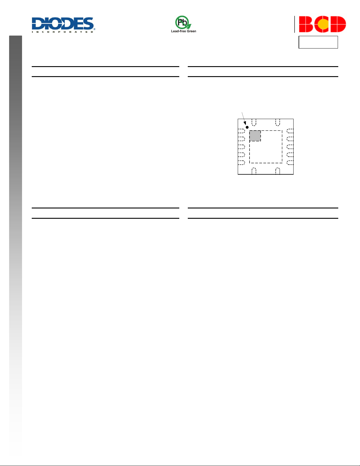
Pin Assignments
(Top View)
U-QFN3535-14
Applications
Notebook Computer, AIO PC
Low-voltage Distribute Power
I/O Supplies
VOUT
VDD
FB
PGOOD
GND
PGND
LGATE
EN/DEM
TON
BOOT
UGATE
PHASE
CS
VDDP
Pin 1 Mark
EP
1 14
2
3
4
5
6
7 8
9
10
11
12
13
SINGLE PHASE SYNCHRONOUS BUCK CONTROLLER
Notes: 1. No purposely added lead. Fully EU Directive 2002/95/EC (RoHS) & 2011/65/EU (RoHS 2) compliant.
2. See http://www.diodes.com/quality/lead_free.html for more information about Diodes Incorporated’s definitions of Halogen - and Antimony-free, "Green"
and Lead-free.
3. Halogen- and Antimony-free "Green” products are defined as those which contain <900ppm bromine, <900ppm chlorine (<1500ppm total Br + Cl) and
<1000ppm antimony compounds.
Page 2
AP3591
Document number: DS36906 Rev. 1 - 2
2 of 18
www.diodes.com
March 2014
© Diodes Incorporated
AP3591
NE W P R OD U CT
A Product Line of
Diodes Incorporated
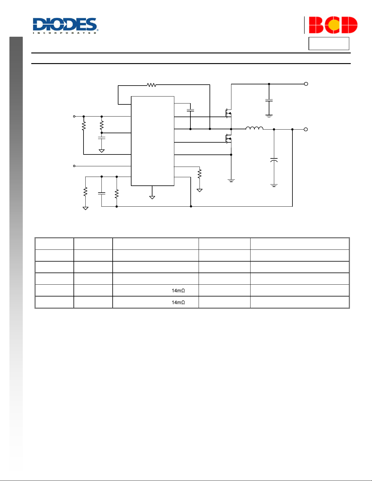
VDDP
BOOT
UGATE
LGATE
PHASE
VOUT
PGOOD
EN/DEM
FB
AP3591
13
14
12
9
5
4
GND
7
L
1.0
C
4
220
mF
R1
C2
C1
10
mF
TON
Q2
Q1
C3
0.1mF
R3
PGND
VDD
VDDP
CCM/ DEM
CS
mH
1
2
3
6
8
10
11
1
mF
C
Optional
10
R2
100K
250K
R4
18K
12K
R5
R6
30K
V
OUT
=1.05V
=12V
V
IN
Symbol
Value
Description
Manufacturer
Part Number
C1
10µF/25V
ESR < 4mΩ @400kHz
Murata
GRM31CR61E106KA12
C4
220µF/6.3V
ESR < 9mΩ @300kHz
Sanyo
6SVPE220M
L
1.0µH
DCR < 4mΩ, I
MAX
= 24A
Vishay
IHLP5050CEER1R0M01
Q1
N-MOSFET
I
DMAX
= 30A, R
DS(ON)
=
Infineon
BSC119N03S
Q2
N-MOSFET
I
DMAX
= 30A, R
DS(ON)
=
Infineon
BSC119N03S
Typical Applications Circuit
BOM
Page 3
AP3591
Document number: DS36906 Rev. 1 - 2
3 of 18
www.diodes.com
March 2014
© Diodes Incorporated
AP3591
NE W P R OD U CT
A Product Line of
Diodes Incorporated
Pin Number
Pin Name
Function
1
EN/DEM
Enable/Diode Emulation Mode control input. Connect to VDD for DEM mode;
connect to GND for shutdown and float the pin for CCM mode
2
TON
On time/Frequency adjustment pin. Connect to PHASE through a resistor. TON
is an input for the PWM controller
3
VOUT
Output voltage pin. Connect to the output of PWM converter. VOUT is an input
for the PWM controller
4
VDD
Analog supply voltage input for the internal analog integrated circuit. Bypass to
GND with a 1µF ceramic capacitor
5
FB
Feedback input pin. Connect FB pin to a resistor voltage divider from VOUT to
GND to adjust V
OUT
from 0.75V to 3.3V
6
PGOOD
Power good signal open-drain output for PWM converter. This pin will be pulled
high when the output voltage is within the target range
7
GND
Analog Ground 8 PGND
Power Ground
9
LGATE
Low-side N-MOSFET gate driver output for the PWM converter. This pin swings
between PGND and VDDP
10
VDDP
VDDP is the gate driver supply for external MOSFETs. Bypass to GND with a
1µF ceramic capacitor
11
CS
Over current trip point set input. Connect a resistor from this pin to signal ground
to set threshold for both over current limit and negative over current limit
12
PHASE
The UGATE High-side gate driver return. Also serves as anode of over current
comparator
13
UGATE
High-side N-MOSFET floating gate driver output for the PWM converter. This pin
swings between PHASE and BOOT
14
BOOT
Bootstrap pin. A bootstrap capacitor is connected for PWM converter. Connect
to an external ceramic capacitor to PHASE
–
Exposed Pad
The exposed pad must be soldered to a large PCB and connected to GND for
maximum power dissipation
Pin Descriptions
Page 4
AP3591
Document number: DS36906 Rev. 1 - 2
4 of 18
www.diodes.com
March 2014
© Diodes Incorporated
AP3591
NE W P R OD U CT
A Product Line of
Diodes Incorporated
Min. t
OFF
1-SHOT
Q
S1
Latch
On-time
Compute
1-SHOT
TRIG
GM
V
REF
SS
(internal)
125% V
REF
70% V
REF
Q
S1
Latch
OV
UV
TRIG
Q
90% V
REF
SS Timer
Thermal
Shutdown
Diode
Emulation
Q
R
S
DRV
DRV
GM
5
2
3
4
1
7
6
8
9
10
12
13
14
11
10mA
VOUT
TON
FB
EN/DEM
GND
CS
PGOOD
PGND
LGATE
VDDP
PHASE
UGATE
BOOT
VDD
Functional Block Diagram
Page 5
AP3591
Document number: DS36906 Rev. 1 - 2
5 of 18
www.diodes.com
March 2014
© Diodes Incorporated
AP3591
NE W P R OD U CT
A Product Line of
Diodes Incorporated
Symbol
Parameter
Rating
Unit
VDD, V
DDP
Supply Voltage
-0.3 to 6
V
VBS
BOOT Pin Voltage
-0.3 to V
PHASE
+6
V
V
UGATE
Voltage from UGATE to PHASE
-0.3 to 6
V
V
LGATE
Voltage from LGATE to GND
-0.3 to 6
V
V
PHASE
Voltage from PHASE to GND
-0.3 to 36
V
V
PGND
Voltage from PGND to GND
-0.3 to 0.3
V
–
Voltage from Other Pins to GND
-0.3 to 6
V
JA
Thermal Resistance (Junction to Ambient)
60
C/W
TJ
Operating Junction Temperature
+150
C
T
STG
Storage Temperature
-65 to +150
C
T
LEAD
Lead Temperature (Soldering, 10Secs)
+260
C
V
HBM
ESD (Human Body Model)
2000
V
VMM
ESD (Machine Model)
200
V
Symbol
Parameter
Min
Max
Unit
VDD, V
DDP
Supply Voltage
4.5
5.5
V
VIN
Input Voltage
4.5
26
V
V
OUT(MAX)
Maximum Output Voltage
–
5.5
V
TA
Operating Ambient Temperature
-40
+85
ºC
Absolute Maximum Ratings (Note 4)
Note 4: Stresses greater than those listed under “Absolute Maximum Ratings” may cause permanent damage to the device. These are stress ratings only, and
functional operation of the device at these or any other conditions beyond those indicated under “Recommended Operating Conditions” is not implied.
Exposure to “Absolute Maximum Ratings” for extended periods may affect device reliability.
Recommended Operating Conditions
Page 6
AP3591
Document number: DS36906 Rev. 1 - 2
6 of 18
www.diodes.com
March 2014
© Diodes Incorporated
AP3591
NE W P R OD U CT
A Product Line of
Diodes Incorporated
Symbol
Parameter
Conditions
Min
Typ
Max
Unit
SUPPLY INPUT
VIN
Input Voltage
–
4.5 – 26
V
I
Q-CCM
Quiescent Current
VDD+VDDP current,
CCM, EN floating, V
FB
=
0.8V
–
500
800
µA
I
Q-DEM
VDD+V
DDP
current, DEM,
V
EN
= 5V, V
FB
= 0.8V
–
500
800
µA
I
SHDN
Shutdown Current
VDD+V
DDP
current, DEM,
V
EN
= 0V
– 1 10
µA
ON-TIME TIMER, OSCILLATOR FREQUENCY AND SOFT START
tON
On Time
V
PHASE
= 12V, V
OUT
=
2.5V, R
ON
= 200kΩ
510
630
750
ns
V
PHASE
= 12V, V
OUT
=
1.05V, R
ON
= 200kΩ
190
260
330
t
OFF-MIN
Min Off Time
–
250
400
580
ns
t
SS
Internal Soft Start Time
–
0.82
1.2
1.5
ms
PWM CONTROLLER GATE DRIVERS
R
U_PH
Upper Gate Pull-up Resistance
V
BOOT-VPHASE
= 5V,
50mA source current
–
3.3 7 Ω
R
U_GATE
Upper Gate Sink Resistance
V
BOOT-VPHASE
= 5V,
50mA sink current
– 1 3
Ω
R
L_PH
Lower Gate Pull-up Resistance
– – 1.8 4 Ω
R
L_GATE
Lower Gate Sink Resistance
V
BOOT-VPHASE
= 5V,
50mA source current
–
0.5 2 Ω
–
PHASE Falling to LGATE
Rising Delay
V
PHASE
< 1.2V to
V
LGATE
> 1.2V
–
30 – ns
–
LGATE Falling to UGATE
Rising Delay
V
LGATE
< 1.2V to
(V
UGATE-VPHASE
) > 1.2V
–
30 – ns
V
BOOT
Boot Diode Forward Voltage
V
DDP-VBOOT
, I
BOOT
=
10mA
0.5
0.83 1 V
I
BSLK
VBS Leakage Current
V
BOOT
= 34V, V
PHASE
=
28V
–
0.1 1 µA
POWER GOOD
–
PGOOD Threshold
PGOOD from low to high
92.5
95
97.5
%
–
PGOOD from high to low
102
105
107
%
–
PGOOD Lower Threshold
Hysteresis
– – ±5 – %
V
PG_L
PGOOD Low Voltage
– – –
0.4
V
I
PG_LEAK
PGOOD Output Leakage
Current
V
PGOOD
= 5V
– – 1
µA
t
DELAY
PGOOD Delay Time
Delay for PGOOD pin
16
22
36
µs
Electrical Characteristics (V
= 12V, V
IN
DD
= V
DDP
= 5V, V
= 1.05V, TA = +25oC, unless otherwise specified.)
OUT
Page 7

AP3591
Document number: DS36906 Rev. 1 - 2
7 of 18
www.diodes.com
March 2014
© Diodes Incorporated
AP3591
NE W P R OD U CT
A Product Line of
Diodes Incorporated
Symbol
Parameter
Conditions
Min
Typ
Max
Unit
VOUT AND REFERENCE VOLTAGE
V
OUT
Output Voltage
–
0.75 – 5.5
V
R
DISCHARGE
Output Discharge Resistance
V
EN
= 0V
–
20 – Ω
VFB
Feedback Voltage
V
DD
= 4.5V to 5.5V
0.742
0.75
0.758
V
IFB
Feedback Bias Current
V
FB
= 0.75V
-1 – 1
µA
PROTECTION
IOC
Current Limit Source Current
CS to GND
9
10
11
µA
–
IOC Temperature Coefficient
– – 4500
–
ppm/oC
V
ILIM_SET
Current Limit Setting Voltage
Range
CS to GND
30 – 200
mV
V
OCL_OFFSET
Over Current Limit Comparator
Offset Voltage
V
CS
= 60mV,
V
CS-GND-VPGND-PHASE
-10 0 10
mV
V
ZC_OFFSET
Zero Crossing Comparator
Offset Voltage
V
PHASE
to GND, V
EN
=
5V
-10 0 10
mV
V
UCL_OFFSET
Negative Over Current Limit
Comparator Offset Voltage
EN floating, V
CS
= 60mV,
V
CS-GND-VPHASE-PGND
-10 0 10
mV
V
FBOV
/VFB
Feedback Over Voltage
Threshold
–
120
125
130
%
t
FBOV_D
Feedback Over Voltage Delay
Time
– – 33 – µs
V
FBUV
/VFB
Feedback Under Voltage
Threshold
–
65
70
75
%
t
FBUV_D
Feedback Under Voltage
Protection Delay Time
– – 28 – µs
t
FBUV_EN_D
Feedback Under Voltage
Protection Enable Delay Time
–
1.3 2 3.1
ms
V
UVLO
VDD Under Voltage Lock
Threshold
VDD Rising
3.7
3.9
4.1
V
V
HYS
VDD Under Voltage Lock
Hysteresis
– – 300 – mV
T
OTSD
Thermal Shutdown
– – +160
– oC
T
HYS
Thermal Shutdown Hysteresis
– – +20
– oC
LOGIC THRESHOLD
V
ENH
EN Control Logic Input Voltage
Setting DEM mode
2.4
2.65
2.9
V
V
ENH-HYS
Hysteresis
–
25 – mV
V
EN_FT
Setting PWM-only mode
1.9
1.96 2 V
V
ENL
Shutdown Threshold
0.8
1.24
1.6
V
V
ENL-HYS
Hysteresis
–
65 – mV
I
EN_PH
EN Pull_up Current
V
EN
= 0V
– 1 –
µA
Electrical Characteristics (Cont. V
= 12V, V
IN
DD
= V
DDP
= 5V, V
= 1.05V, TA = +25oC, unless otherwise specified.)
OUT
Page 8

AP3591
Document number: DS36906 Rev. 1 - 2
8 of 18
www.diodes.com
March 2014
© Diodes Incorporated
AP3591
NE W P R OD U CT
A Product Line of
Diodes Incorporated
0 2000 4000 6000 8000 10000 12000
0
20
40
60
80
100
Efficiency (%)
Load Current (mA)
VIN = 8V
VIN = 12V
VIN = 20V
0 2000 4000 6000 8000 10000 12000
0
20
40
60
80
100
Efficiency (%)
Load Current (mA)
VIN = 8V
VIN = 12V
VIN = 20V
0 2000 4000 6000 8000 10000 12000
0
20
40
60
80
100
Efficiency (%)
Load Current (mA)
DEM
CCM
0 100 200 300 400 500 600 700 800 900
0
100
200
300
400
500
600
700
800
900
1000
1100
Frequency (KHz)
RT ()
V
OUT
= 1.05V
V
OUT
= 2.5V
-2 0 2 4 6 8 10 12 14 16
100
150
200
250
300
350
400
Frequency (KHz)
Load Current (A)
VIN = 8V
VIN = 12V
VIN = 20V
5 10 15 20 25 30
100
150
200
250
300
350
400
Frequency (KHz)
VIN (V)
V
OUT
= 1.05V@0A
V
OUT
= 1.05V@10A
V
OUT
= 2.5V@0A
V
OUT
= 2.5V@10A
Performance Characteristics
Efficiency vs. Load Current @V
Efficiency vs. Load Current (CCM vs. DEM) Frequency vs. RT
= 1.05V Efficiency vs. Load Current @V
OUT
Frequency vs. Load Current Frequency vs. VIN
OUT
= 2.5V
Page 9

AP3591
Document number: DS36906 Rev. 1 - 2
9 of 18
www.diodes.com
March 2014
© Diodes Incorporated
AP3591
NE W P R OD U CT
A Product Line of
Diodes Incorporated
6 8 10 12 14 16 18 20 22 24 26
0.0
0.5
1.0
1.5
2.0
Shutdown Current (
mA)
VIN (V)
-40 -20 0 20 40 60 80 100 120 140 160
7
8
9
10
11
12
13
14
15
I
CS
(mA)
Temperature (oC)
V
OUT
2V/div
V
PHASE
10V/div
VEN
1V/div
IL
2.5A/div
Time 2ms/div
V
OUT
2V/div
V
PHASE
10V/div
VEN
2V/div
IL
5A/div
Time 1ms/div
V
OUT
2V/div
V
PHASE
10V/div
VDD
1V/div
IL
5A/div
Time 1ms/div
V
OUT
2V/div
V
PHASE
10V/div
VDD
2V/div
IL
5A/div
Time 1ms/div
Performance Characteristics (Cont.)
Shutdown Current vs. V
Power ON from EN @CCM Power ON from EN @DEM
Power ON from VDD @CCM Power ON from VDD @DEM
IN ICS
vs. Temperature (C)
Page 10

AP3591
Document number: DS36906 Rev. 1 - 2
10 of 18
www.diodes.com
March 2014
© Diodes Incorporated
AP3591
NE W P R OD U CT
A Product Line of
Diodes Incorporated
V
OUT
2V/div
VUG
5V/div
VLG
5V/div
V
FB
1V/div
Time 200µs/div
V
OUT
2V/div
VUG
5V/div
IL
10A/div
Time 20µs/div
V
OUT
2V/div
V
PHASE
10V/div
VEN
2V/div
Time 4ms/div
V
OUT
2V/div
V
PHASE
10V/div
VEN
2V/div
Time 4ms/div
V
OUT
100mV/div
I
L
10A/div
Time 1ms/div
V
OUT
100mV/div
I
L
10A/div
Time 1ms/div
VLG
10V/div
Performance Characteristics (Cont.)
OVP UVP
MODE Transition DEM to CCM MODE Transition CCM to DEM
Load Transient Response @ CCM Load Transient Response @ DEM
Page 11

AP3591
Document number: DS36906 Rev. 1 - 2
11 of 18
www.diodes.com
March 2014
© Diodes Incorporated
AP3591
NE W P R OD U CT
A Product Line of
Diodes Incorporated
f
IN
OUT
ON
V
V
t
ON
t
2L
VV
I
OUTIN
LOAD
Application Information
1. Functional Description
The AP3591 is a synchronous step-down controller. Adaptive constant on time (COT) control is employed to provide fast transition response and
easy loop stabilization. AP3591 does not have a dedicated in board oscillator. It runs with a pseudo-constant frequency which is set by RON. The
output voltage variation is sensed by FB Pin. If VFB is below 0.75V, the error comparator will trigger the control logic and generate an ON-time
period, in which high side MOSFET is turned on and low side MOSFET is turned off. The ON-time period length is calculated using the following
equation:
V
is the output voltage, VIN is the input voltage, and f is the switching frequency.
OUT
The on-time is the time required for the voltage on this capacitor charging from zero volts to V
directly proportional to the output voltage and inversely proportional to the input voltage. The implementation results in a nearly constant switching
frequency without the need of a clock generator.
t
= 14.5p×R
ON
After an ON-time period, the AP3591 goes into the OFF-time period. The OFF-time period length depends on VFB in most case. It will end when
VFB decreases below 0.75V and then the ON-time period is triggered again. If the OFF-time period is less than the minimum OFF time, the
minimum OFF time will be applied, which is about 400ns typical.
2. Mode Selection Operation
AP3591 has two operation modes: Continuous Conduction Mode (CCM) and Diode Emulation Mode (DEM). When the EN/DEM pin voltage is
higher than 2.9V, AP3591 will operate in DEM mode for high efficiency; when the EN/DEM pin is floating, AP3591 will operate in forced CCM
mode to a certain frequency during a light load condition.
2.1 Diode Emulation Mode
If the DEM mode is selected, the AP3591 automatically reduces the switching frequency under a light load condition to get high efficiency. When
the output current decreases and heavy load condition is formed, the inductor current decreases as well, and eventually comes close to zero
current, which is the boundary between CCM and DEM. The low side MOSFET will turn off whenever the inductor current reaches zero level. The
load is provided only by the output capacitor. When FB voltage is lower than 0.75V, the next ON cycle is beginning. The ON-time is kept the same
as that in the heavy load condition. The switching frequency increases to keep V
load. The transition load point is calculated using the following equation:
TON
×(V
OUT
+0.1)/VIN+50ns
voltage when the output current increases from light to heavy
OUT
, thereby the ON-time of the high side switch is
OUT
tON is the on-time.
2.2 Continuous Conduction Mode
When AP3591 operates in CCM mode, the duty cycle V
inductor current decreases to reverse. The benefit of CCM is to keep the switching frequency fairly constant to avoid a certain frequency during a
light load condition.
3. Power On Reset and Soft-start
Power on reset occurs when VDD rises above approximately 3.9V: the IC will reset the fault latch and prepare the PWM for operation. When VDD is
below 3.6V, the VDD under voltage lockout (UVLO) circuitry inhibits switching by keeping UGATE and LGATE low. A built-in soft-start is used to
prevent surge current from power supply input VIN during turn on (referring to Functional Block Diagram). The error amplifier is a three-input device.
Reference voltage V
amplifier. VSS internally ramps up to 95% of 0.75V in 1.2ms for AP3591 after the soft-start cycle is initiated.
Figure 1 shows a typical start-up interval for AP3591 when the EN/DEM pin has been released from a grounded (system shutdown) state.
is not changed at light load condition. The low side MOSFET keeps on even when
OUT/VIN
or the internal soft-start voltage VSS whichever is smaller dominates the behavior of the non-inverting inputs of the error
REF
Page 12

AP3591
Document number: DS36906 Rev. 1 - 2
12 of 18
www.diodes.com
March 2014
© Diodes Incorporated
AP3591
NE W P R OD U CT
A Product Line of
Diodes Incorporated
T0
T1
T2
V
OUT
Normal
V
OUT
Pre-Biased
V
OUT
Over-Charged
GND
V
OUT
1V/div
V
UGATE
20V/div
VEN
2V/div
V
PGOOD
5V/div
Time 400µs/div
Application Information (Cont.)
Power On from EN (DEM Mode)
Figure 1. Start-up Behavior of AP3591
4. Power Good Output
The AP3591 features power good output to monitor the output voltage. It is an open-drain output and should be connected to a 5V power supply
node through a resistor. The power good function is active after the soft start is finished. PGOOD signal becomes high if output voltage reaches
±5% of the target value after 64µs delay building into the PGOOD circuitry. It will become low immediately if the output voltage goes beyond ±10%
of the target value.
5. Soft Stop
The AP3591 has a built in soft-stop circuitry. The output is discharged with an internal 20Ω transistor when EN/DEM is low or the device is in a
fault condition including UVLO and OTP. The discharge time constant is determined by the output capacitance and resistance of the discharge
transistor.
6. Pre-biased Output
Figure 2 shows the normal V
to a voltage less than the expected value, as shown by the magenta curve, the AP3591 will detect that condition. Neither MOSFET will turn on
until the soft-start ramp voltage exceeds the output. V
expected value, as showed in the black curve, neither MOSFET will turn on until the output voltage is pulled down to the expected value through
external load. Any resistive load connected to the output will help pull down the voltage.
start-up curve in blue; Initialization begins at T0, and output ramps between T1 and T2. If the output is pre-biased
OUT
starts seamlessly ramping from there. If the output is pre-biased to a voltage above the
OUT
Figure 2. Start-up Behavior with Pre-biased Output Voltage
Page 13

AP3591
Document number: DS36906 Rev. 1 - 2
13 of 18
www.diodes.com
March 2014
© Diodes Incorporated
AP3591
NE W P R OD U CT
A Product Line of
Diodes Incorporated
OC
COMPARATOR
CURRENT SENSE
Ioc
OPS
ROC-SET
Q1
Q2
REVERSE BUFFER
)(RA10)(V
SET-OCCS
KmV
m
IN
OUTOUTIN
PP
L
V
VVV
fL
V
I
V
)(
2
1
R
2R
I
DS(ON)
CS
)(
DS(ON)
CS
O_OCSET
Application Information (Cont.)
7. Over Current Protection (OCP)
Figure 3 shows the over current protection (OCP) scheme of AP3591. In each switching cycle, the inductor current is sensed by monitoring the
low-side MOSFET in the OFF period. When the voltage between PGND pin and PHASE pin is larger than the over current trip level, the OCP is
triggered and the controller keeps the OFF state. Because the R
temperature coefficient to compensate this temperature dependency of R
A resistor R
the OCP trip point I
The load current at over-current threshold (I
V
OUT
8. Negative Over Current Protection (NOCP)
The AP3591 supports cycle by cycle negative over current limiting in CCM mode. The over current limit value is the same absolute value as the
positive over current limit. If the inductor reverse current is larger than NOCP current at OFF time, the LMOSFET is turned off. The reverse current
will flows to VIN through the body diode of HMOSFET. After 400ns delay, LMOSFET is turned on again. If the NOCP is released, the HMOSFET
is turned on and the device resumes normal operation.
9. Under Voltage Protection (UVP)
The output voltage is also monitored for under voltage protection. When the output voltage is less than 70% of the setting voltage threshold, under
voltage protection is triggered after 28µs delay to prevent false transition. When UVP is triggered, UGATE and LGATE will get low, and the output
is discharged with the internal 20Ω transistor. UVP is a latched protection; it can only be released by VDD or EN/DEM power-on reset. The UVP
blanking time is 2ms during soft-start.
10. Under Voltage Lockout
The AP3591 provides an under voltage lockout circuit to prevent from undefined status at startup. The UVLO circuit shuts down the device when
VDD drops below 3.6V. The UVLO circuit has 300mV hysteresis, which means the device will start up again when VDD rises to 3.9V.
11. Over Voltage Protection (OVP)
The feedback voltage is continuously monitored for over voltage protection. When OVP is triggered, LGATE will go high and UGATE will go low to
discharge the output capacitor.
OC-SET
is the output voltage, ΔI
of MOSFET increases with the temperature, IOC has 4500ppm/ºC
DS(ON)
.
DS(ON)
Figure 3. Over Current Scheme
should be connected from CS pin to GND. An internal current source IOC (10µA typically), flowing through R
, which can be calculated using the following equation:
OCSET
), can be calculated using the following equation:
O_OCSET
is the inductor current ripple peak to peak value and f is the switching frequency.
L(PP)
OC-SET
determines
Page 14

AP3591
Document number: DS36906 Rev. 1 - 2
14 of 18
www.diodes.com
March 2014
© Diodes Incorporated
AP3591
NE W P R OD U CT
A Product Line of
Diodes Incorporated
V
OUT
1V/div
V
LGATE
5V/div
Time 100µs/div
V
UGATE
20V/div
Application Information (Cont.)
The AP3591 provides full-time over voltage protection whenever soft-start completes or not. The typical OVP threshold is 125% of the internal
reference voltage V
built into the over voltage protection circuit to prevent false transitions.
. The AP3591 provides latched OVP and can only be released by VDD or EN/DEM power-on reset. There is 33µs delay
REF
Figure 4. Over Voltage Protection
12. Thermal Shutdown
If the junction temperature of the device reaches the thermal shutdown limit of +160ºC, the AP3591 shuts itself off. Both UGATE and LGATE are
driven low, turning off both MOSFETs. The output is discharged with the internal 20Ω transistor. When the junction temperature cools down to the
required level (+140°C nominal), the device initiates soft-start as during a normal power-up cycle.
Page 15

AP3591
Document number: DS36906 Rev. 1 - 2
15 of 18
www.diodes.com
March 2014
© Diodes Incorporated
AP3591
NE W P R OD U CT
A Product Line of
Diodes Incorporated
PackingPackageProduct Name
TR : Tape & Reel
G1 : Green
AP3591 XX XX – XX
RoHS/Green
FN : U-QFN3535-14
Package
Temperature
Range
Part Number
Marking ID
Packing
U-QFN3535-14
-40 to +85C
AP3591FNTR-G1
BHA
5000/Tape & Reel
First Line: Logo and Marking ID
Second and Third Lines: Date Code
Y: Year
WW: Work Week of Molding
A: Assembly House Code
XX: 7th and 8th Digits of Batch No.
Ordering Information
Diodes IC’s Pb-free products with "G1" suffix in the part number, are RoHS compliant and green.
Marking Information
(1) U-QFN3535-14
(Top View)
Page 16

AP3591
Document number: DS36906 Rev. 1 - 2
16 of 18
www.diodes.com
March 2014
© Diodes Incorporated
AP3591
NE W P R OD U CT
A Product Line of
Diodes Incorporated
3.400(0.134)
3.600(0.142)
3.400(0.134)
3.600(0.142)
1.900(0.075)
2.100(0.083)
1.500(0.059)
BSC
0.500(0.020)
BSC
0.350(0.014)
0.450(0.018)
0.200(0.008)
0.300(0.012)
0.750(0.030)
0.900(0.035)
0.000(0.000)
0.050(0.002)
A1
Pin 1 Mark
PIN #
1 IDENTIFICATION
See DETAIL A
1
DETAIL A
Pin 1 options
N1
N2
N6
N8
N13
N14
2
3
4
1
2
3
4
1
2
3
4
Symbol
A1
min(mm) max(mm) min(inch) max(inch)
Option1
Option2
0.203(REF)
0.150(REF)
0.008(REF)
0.006(REF)
1.900(0.075)
2.100(0.083)
Package Outline Dimensions (All dimensions in mm(inch).)
(1) Package Type: U-QFN3535-14
Page 17

AP3591
Document number: DS36906 Rev. 1 - 2
17 of 18
www.diodes.com
March 2014
© Diodes Incorporated
AP3591
NE W P R OD U CT
A Product Line of
Diodes Incorporated
E2
X2
X1
Y1
Y2
E1
Y3
X3
X
Y
Dimensions
X=Y
(mm)/(inch)
X1=Y1
(mm)/(inch)
X2=Y2
(mm)/(inch)
X3=Y3
(mm)/(inch)
E1
(mm)/(inch)
E2
(mm)/(inch)
Value
3.800/0.150
2.100/0.083
0.650/0.026
0.300/0.012
0.500/0.020
1.500/0.059
Suggested Pad Layout
(1) Package Type: U-QFN3535-14
Page 18

AP3591
Document number: DS36906 Rev. 1 - 2
18 of 18
www.diodes.com
March 2014
© Diodes Incorporated
AP3591
NE W P R OD U CT
A Product Line of
Diodes Incorporated
DIODES INCORPORATED MAKES NO WARRANTY OF ANY KIND, EXPRESS OR IMPLIED, WITH REGARDS TO THIS DOCUMENT,
INCLUDING, BUT NOT LIMITED TO, THE IMPLIED WARRANTIES OF MERCHANTABILITY AND FITNESS FOR A PARTICULAR PURPOSE
(AND THEIR EQUIVALENTS UNDER THE LAWS OF ANY JURISDICTION).
Diodes Incorporated and its subsidiaries reserve the right to make modifications, enhancements, improvements, corrections or other changes
without further notice to this document and any product described herein. Diodes Incorporated does not assume any liability arising out of the
application or use of this document or any product described herein; neither does Diodes Incorporated convey any license under its patent or
trademark rights, nor the rights of others. Any Customer or user of this document or products described herein in such applications shall assume
all risks of such use and will agree to hold Diodes Incorporated and all the companies whose products are represented on Diodes Incorporated
website, harmless against all damages.
Diodes Incorporated does not warrant or accept any liability whatsoever in respect of any products purchased through unauthorized sales channel.
Should Customers purchase or use Diodes Incorporated products for any unintended or unauthorized application, Customers shall indemnify and
hold Diodes Incorporated and its representatives harmless against all claims, damages, expenses, and attorney fees arising out of, directly or
indirectly, any claim of personal injury or death associated with such unintended or unauthorized application.
Products described herein may be covered by one or more United States, international or foreign patents pending. Product names and markings
noted herein may also be covered by one or more United States, international or foreign trademarks.
This document is written in English but may be translated into multiple languages for reference. Only the English version of this document is the
final and determinative format released by Diodes Incorporated.
Diodes Incorporated products are specifically not authorized for use as critical components in life support devices or systems without the express
written approval of the Chief Executive Officer of Diodes Incorporated. As used herein:
A. Life support devices or systems are devices or systems which:
1. are intended to implant into the body, or
2. support or sustain life and whose failure to perform when properly used in accordance with instructions for use provided in the
labeling can be reasonably expected to result in significant injury to the user.
B. A critical component is any component in a life support device or system whose failure to perform can be reasonably expected to cause the
failure of the life support device or to affect its safety or effectiveness.
Customers represent that they have all necessary expertise in the safety and regulatory ramifications of their life support devices or systems, and
acknowledge and agree that they are solely responsible for all legal, regulatory and safety-related requirements concerning their products and any
use of Diodes Incorporated products in such safety-critical, life support devices or systems, notwithstanding any devices- or systems-related
information or support that may be provided by Diodes Incorporated. Further, Customers must fully indemnify Diodes Incorporated and its
representatives against any damages arising out of the use of Diodes Incorporated products in such safety-critical, life support devices or systems.
Copyright © 2014, Diodes Incorporated
www.diodes.com
IMPORTANT NOTICE
LIFE SUPPORT
 Loading...