

Page 1
Single Phase Synchronous Buck PWM Controller AP3586A/B/C
Data sheet
General Description
The AP3586A/B/C is a compact synchronous
-rectified buck controller specifically designed to
operate from 5V or 12V supply voltage and deliver
high-quality output voltage as low as 0.6V
(AP3586A) or 0.8V (AP3586B/C). This device
operates at fixed 300kHz (AP3586A/B) or 200kHz
(AP3586C) frequency and provides an optimal level
of integration to reduce size and cost of the power
supply.
This controller integrates internal MOSFET drivers
that support 12V+12V bootstrapped voltage for highefficiency power conversion. The bootstrap diode is
built-in to simplify the circuit design and minimize
external part count.
This controller provides single feedback loop,
voltage-mode control with fast transient response.
The error amplifier features a 10MHz gain-bandwidth
product and 6V/µs slew rate which enables high
converter bandwidth for fast transient performance.
Other features include internal soft-start, under
voltage protection, over current protection and
shutdown function. With afore-mentioned functions,
this part provides customers a compact, high
efficiency, well-protected and cost-effective
solutions.
The AP3586A/B/C is available in SOIC-8 and
PSOP-8 packages.
Figure 1. Package Types of AP3586A/B/C
SOIC-8/PSOP-8
Features
• Supply Voltage: 5V/12V
• V
• 0.6V/0.8V to 82% of V
• Internal Reference: 0.6V/0.8V
• Simple Single-loop Control
• Voltage-mode PWM Control
• Duty Cycle: 0% to 82%
• Fast Transient Response
• 10MHz High-bandwidth Error Amplifier with
• Fixed Oscillator Frequency: 300kHz/200kHz
• Lossless, Programmable Over Current Protection
• Start-up into Pre-biased Load
• Built-in Thermal Shutdown
• Built-in Soft-start
• Over Current Protection
• Over Voltage Protection
• Under Voltage Protection
• Integrated Boot Diode
Input Range: 3.3V to 12V
IN
IN
6V/µs Slew Rate
(Uses Lower MOSFET R
Output Range
)
DS(ON)
Applications
• Subsystem Power Supplies
• PCI, AGP, Graphics Cards, Digital TV
• SSTL-2 and DDR/2/3 SDRAM Bus Termination
Supply
• Cable Modems, Set Top Boxes, and DSL
Modems
• Industrial Power Supplies and General Purpose
Supplies
Mar. 2012 Rev. 1. 1 BCD Semiconductor Manufacturing Limited
1
Page 2
Data sheet
Single Phase Synchronous Buck PWM Controller AP3586A/B/C
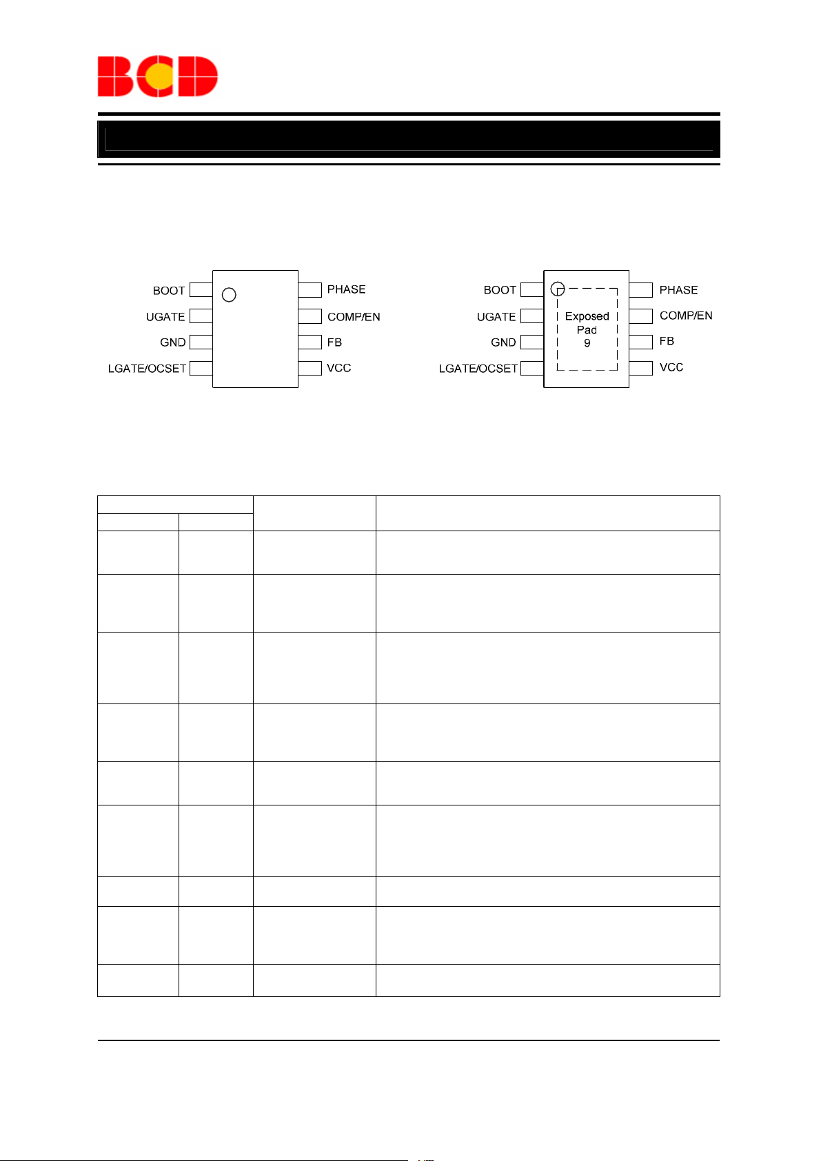
Pin Configuration
M Package
(SOIC-8)
MP Package
(PSOP-8)
1
2
3
4
Figure 2. Pin Configuration of AP3586A/B/C (Top View)
8
7
6
5
Pin Description
Pin Number
SOIC-8 PSOP-8
1 1 BOOT
2 2 UGATE
3 3 GND
4 4 LGATE/OCSET
5 5 VCC
6 6 FB
7 7 COMP/EN
8 8 PHASE
9 Exposed Pad
Pin Name Function
1
2
3
4
8
7
6
5
Bootstrap pin. Connect a bootstrap capacitor from this pin to
PHASE for creating a BOOT voltage suitable to drive a standard
N-Channel MOSFET.
Upper-gate drive pin. Connect this pin to the upper MOSFET gate
providing the gate drive. This pin is monitored by the adaptive
shoot-through protection circuitry to determine when the upper
MOSFET has turned off.
Ground for the IC. All voltage levels are measured with respect to
this pin. Connect this pin directly to the low side MOSFET source
and ground plane with the lowest impedance. The exposed pad
must be soldered to a large PCB and connected to GND for
maximum power dissipation.
Low-side Gate Driver Output and Over-Current Setting Input.
This pin is the gate driver for low-side MOSFET. It is also used to
set the maximum inductor current. Refer to the section in
“Function Description” for detail.
Bias supply pin. Provides a 5V or 12V bias supply for the chip
from this pin. The pin should be bypassed with a capacitor to
GND.
Feedback pin. This pin is the inverting input of the internal error
amplifier. Use FB pin, in combination with the COMP pin, to
compensate the voltage control feedback loop of the converter. A
resistor divider from output to GND is used to set the output
voltage.
Compensation and disable pin. This pin is the output of the Error
Amplifier. Pull COMP pin low will shut down the IC.
This pin connects to the source of the upper MOSFET and the
drain of the lower MOSFET. This pin is also monitored by the
adaptive shoot-through protection circuitry to determine when the
upper MOSFET has turned off.
Exposed Pad as ground pin.
Mar. 2012 Rev. 1. 1 BCD Semiconductor Manufacturing Limited
2
Page 3
Data sheet
Single Phase Synchronous Buck PWM Controller AP3586A/B/C
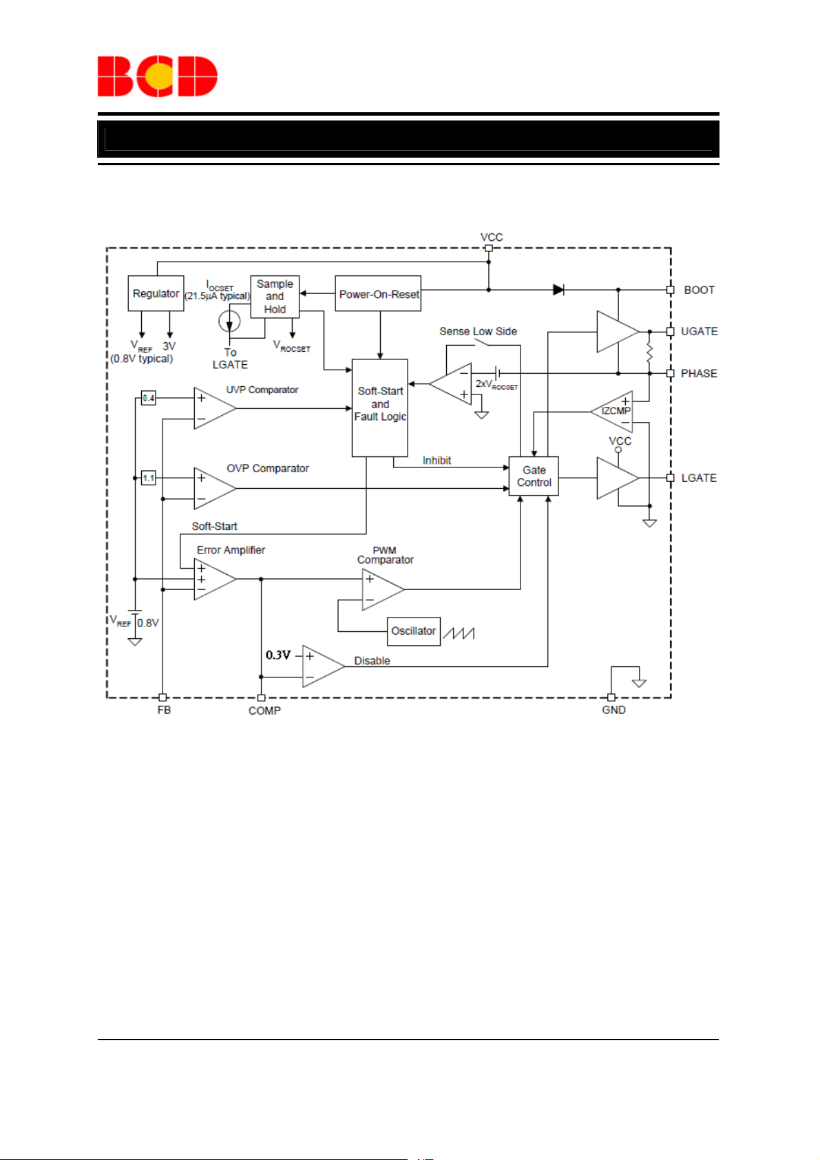
Functional Block Diagram
5
1
2
8
4
/0.6V
6
7
/EN
Figure 3. Functional Block Diagram of AP3586A/B/C
3
/OCSET
Mar. 2012 Rev. 1. 1 BCD Semiconductor Manufacturing Limited
3
Page 4
Data sheet
Single Phase Synchronous Buck PWM Controller AP3586A/B/C
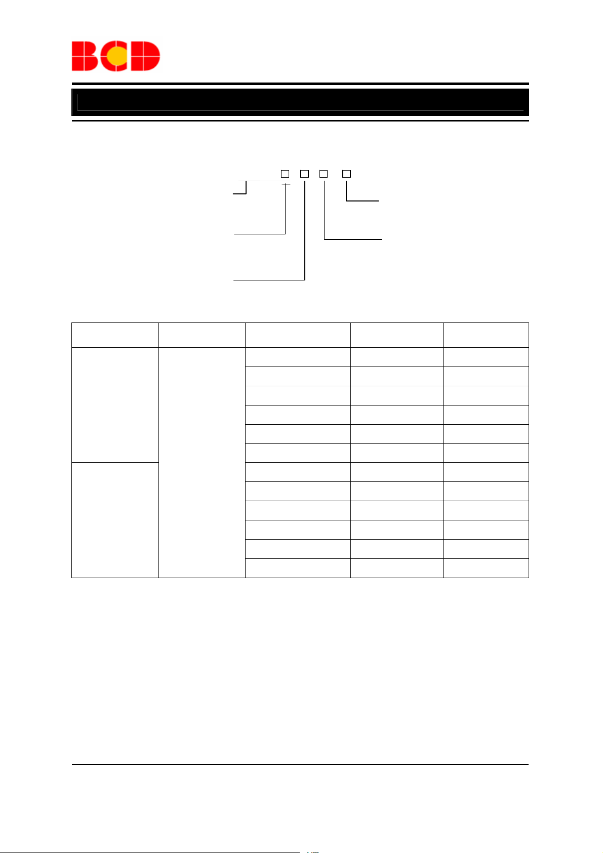
Ordering Information
AP3586 -
G1: Green
Blank: Tube
TR: Tape & Reel
Package
Circuit Type
A: AP3586A
B: AP3586B
C: AP3586C
Package
M: SOIC-8
MP: PSOP-8
Temperature
Range
Part Number Marking ID Packing Type
AP3586AM-G1 3586AM-G1 Tube
AP3586AMTR-G1 3586AM-G1 Tape & Reel
SOIC-8
-40 to 85°C
PSOP-8
AP3586BM-G1 3586BM-G1 Tube
AP3586BMTR-G1 3586BM-G1 Tape & Reel
AP3586CM-G1 3586CM-G1 Tube
AP3586CMTR-G1 3586CM-G1 Tape & Reel
AP3586AMP-G1 3586AMP-G1 Tube
AP3586AMPTR-G1 3586AMP-G1 Tape & Reel
AP3586BMP-G1 3586BMP-G1 Tube
AP3586BMPTR-G1 3586BMP-G1 Tape & Reel
AP3586CMP-G1 3586CMP-G1 Tube
AP3586CMPTR-G1 3586CMP-G1 Tape & Reel
BCD Semiconductor's Pb-free products, as designated with "G1" suffix in the part number, are RoHS compliant
and green.
Mar. 2012 Rev. 1. 1 BCD Semiconductor Manufacturing Limited
4
Page 5
Data sheet
Single Phase Synchronous Buck PWM Controller AP3586A/B/C
Absolute Maximum Ratings (Note 1)
Parameter Symbol Value Unit
Supply Input Voltage
BOOT Voltage
UGATE to PHASE Voltage V
PHASE, LGATE to GND Voltage
Other Pin Voltage -0.3 to 6 V
Power Dissipation PD TBD mW
Thermal Resistance
Operating Junction Temperature TJ -40 to 125 ºC
Storage Temperature T
Lead Temperature (Soldering, 10 sec) T
ESD (Human Body Model) (Note 2) 2000 V
ESD (Machine Model) (Note 2) 200 V
VCC
V
BOOT
-0.3 to 15 V
UGATE
,
V
PHASE
V
LGATE
θ
JA
-65 to 150 ºC
STG
260 ºC
LEAD
-0.3 to 15 V
-0.3 to V
-1 to 15 V
+15 V
PHASE
50 ºC/W
Note 1: Stresses greater than those listed under “Absolute Maximum Ratings” may cause permanent damage to
the device. These are stress ratings only, and functional operation of the device at these or any other conditions
beyond those indicated under “Recommended Operating Conditions” is not implied. Exposure to “Absolute
Maximum Ratings” for extended periods may affect device reliability.
Note 2: Devices are ESD sensitive. Handling precaution is recommended.
Recommended Operating Conditions
Parameter Symbol Min Max Unit
Supply Input Voltage VCC 5 12 V
Operating Ambient Temperature TA -40 85
°C
Mar. 2012 Rev. 1. 1 BCD Semiconductor Manufacturing Limited
5
Page 6
Data sheet
Single Phase Synchronous Buck PWM Controller AP3586A/B/C
Electrical Characteristics
VCC=12V, TA=25°C, unless otherwise specified.
Parameter Symbol Conditions Min Typ Max Unit
SUPPLY INPUT
Supply Current
Quiescent Supply Current
ICC
I
CC_Q
Power Input Voltage VIN 3.0 13.2 V
POWER ON RESET
VCC Rising Threshold V
VCC Threshold Hysteresis V
POR
POR_HYS
UGATE and LGATE Pins
Open; Switching
V
No Switching
FB=VREF
+0.1V,
VCC Rising
5 mA
4 mA
4.0 4.2 4.4 V
500 mV
OSCILLA TOR
Oscillator Frequency
f
OSC
For AP3586A/B 270 300 330 kHz
For AP3586C 180 200 220 kHz
∆V
Ramp Amplitude
OSC
1.4 V
P-P
ERROR AMPLIFIER
G
Open Loop DC Gain
Gain-bandwidth Product
Slew Rate SR 3 6
Transconductance 800 1100
Output Source Current
Output Sink Current
DC_OL
GBW
55 70 dB
10 MHz
V/µs
µA/V
FB<VREF
FB>VREF
80 120
80 120
µA
µA
V
V
PWM CONTROLLER GATE DRIVERS
Upper Gate Source
Current
Upper Gate Sink Current I
Upper Gate Sink
Resistance
Lower Gate Source
Current
Lower Gate Sink Current I
Lower Gate Sink
Resistance
PHASE Falling to LGATE
Rising Delay
LGATE Falling to UGATE
Rising Delay
V
I
UG_SRC
UG_SNK
R
UGATE
I
LG_SRC
LG_SNK
R
LGATE
V
BOOT-VPHASE
V
BOOT-VUGATE
V
BOOT-VPHASE
V
BOOT-VUGATE
=12V,
=6V
=12V,
=6V
50mA Source Current
VCC-V
V
LGATE
LGATE
=6V
=6V
50mA Source Current
<1.2V to V
PHASE
V
<1.2V to
LGATE
(V
UGATE-VPHASE
LGATE
)>1.2V
-1.0 A
1.5 A
2 4 Ω
-1 A
1.5 A
1 2 Ω
>1.2V 50 ns
50 ns
Mar. 2012 Rev. 1. 1 BCD Semiconductor Manufacturing Limited
6
Page 7

Data sheet
Single Phase Synchronous Buck PWM Controller AP3586A/B/C
Electrical Characteristics (Continued)
VCC=12V, TA=25ºC, unless otherwise specified.
Parameter Symbol Conditions Min Typ Max Unit
Minimum Duty Cycle 0 %
Maximum Duty Cycle 75 82 89 %
REFERENCE VOLT AGE
Feedback Voltage VFB
Feedback Bias Current IFB VFB=5V 10 50 nA
PROTECTION
Under Voltage Protection V
Over Voltage Protection V
OC Current Source I
Built-in Maximum OCP
Voltage
Soft-start Interval tSS
Enable Threshold V
Thermal Shutdown T
Thermal Shutdown
Hysteresis
FB_UVP
FB_OVP
OPS
V
OCP_MAX
COMP/EN
OTSD
T
HYS
AP3586A 0.591 0.6 0.609 V
AP3586B/C 0.788 0.8 0.812 V
0.3 0.4 0.5 V
19.5 21.5 23.5
0.3 V
AP3586A 2
AP3586B 2.7
AP3586C 3.6
0.25 0.30 0.35 V
160 ºC
20 ºC
1.1 V
µA
ms
Mar. 2012 Rev. 1. 1 BCD Semiconductor Manufacturing Limited
7
Page 8

Data sheet
Single Phase Synchronous Buck PWM Controller AP3586A/B/C
Typical Performance Characteristics
1.0
0.5
0.0
-0.5
Output Voltage Variation (%)
-1.0
5678910111213
Input Voltage (V)
4
V
= 1.2V
OUT
3
2
1
0
-1
-2
Output Voltage Variation (%)
-3
-4
0 2 4 6 8 101214161820
Output Current (A)
V
= 1.2V
OUT
Figure 4. Line Regulation Figure 5. Load Regulation
320
315
310
305
300
295
290
285
Switching Frequency (kHz)
280
275
270
-40 -20 0 20 40 60 80 100 120
Figure 6. Switching Frequency vs. Temperature Figure 7. Switching Frequency vs. Input Voltage
Temperature (oC)
320
315
310
305
300
295
290
285
Switching Frequency (kHz)
280
275
270
4 5 6 7 8 9 10 11 12 13 14
Input Voltage (V)
Mar. 2012 Rev. 1. 1 BCD Semiconductor Manufacturing Limited
8
Page 9

Data sheet
Single Phase Synchronous Buck PWM Controller AP3586A/B/C
Typical Performance Characteristics (Continued)
0.810
0.808
0.806
0.804
0.802
0.800
0.798
0.796
Reference Voltage (V)
0.794
0.792
0.790
-40 -20 0 20 40 60 80 100 120
Temperature (oC)
0.810
0.808
0.806
0.804
0.802
0.800
0.798
0.796
Reference Voltage (V)
0.794
0.792
0.790
4567891011121314
Input Voltage (V)
Figure 8. Reference Voltage vs. Temperature Figure 9. Reference Voltage vs. Input Voltage
VIN
10V/div
V
OUT
0.5V/div
V
COMP
0.5V/div
V
LGATE
5V/div
Figure 10. Power-on Waveform Figure 11. Enable Waveform
(VIN=12V, V
Time 1ms/div
=1.2V, I
OUT
=0A) (VIN=12V, V
OUT
5A/div
V
OUT
0.5V/div
V
COMP
1V/div
V
LGATE
20V/div
I
L
Time 2ms/div
OUT
=1.2V, I
OUT
=0A)
Mar. 2012 Rev. 1. 1 BCD Semiconductor Manufacturing Limited
9
Page 10

Data sheet
Single Phase Synchronous Buck PWM Controller AP3586A/B/C
Typical Performance Characteristics (Continued)
V
50mV/div
OUT_AC
V
OUT_AC
50mV/div
I
OUT
2A/div
I
OUT
5A/div
Time 20µs/div
Time 20µs/div
Figure 12. Load Transient Response Figure 13. Load Transient Response
(VIN=12V, V
OUT
=1.2V, I
=0A to 10A) (VIN=12V, V
OUT
OUT
=1.2V, I
=0A to 20A)
OUT
VIN
10V/div
V
OUT
1V/div
V
COMP
1V/div
V
LGATE
5V/div
Figure 14. Over Current Protection
(V
=12V, V
IN
Time 10ms/div
=1.2V, I
OUT
OUT
Figure 15. Under Voltage Protection
=20A) (VIN=12V, V
V
UGATE
10V/div
V
LGATE
20V/div
V
0.5V/div
10A/div
FB
I
L
Time 20ms/div
OUT
=1.2V, I
OUT
=20A)
Mar. 2012 Rev. 1. 1 BCD Semiconductor Manufacturing Limited
10
Page 11

Data sheet
Single Phase Synchronous Buck PWM Controller AP3586A/B/C
Typical Application
Figure 16. Typical Appl ication Circuit of AP3586A/B/C
Mar. 2012 Rev. 1. 1 BCD Semiconductor Manufacturing Limited
11
Page 12

Data sheet
Single Phase Synchronous Buck PWM Controller AP3586A/B/C
Function Description
The AP3586A/B/C is a voltage-mode single phase
synchronous buck controller with embedded
MOSFET drivers. This part provides complete
protection functions such as over voltage protection,
under voltage protection and over current protection.
Inductor current information is sensed by R
DS(ON)
of
the low side MOSFET. The over current protection
threshold can be simply programmed by a resistor.
Power on Reset and Chip Enable
A power on reset (POR) circuitry continuously
monitors the supply voltage at VCC pin. Once the
rising POR threshold is exceeded, the AP3586A/B/C
sets itself to active state and is ready to accept chip
enable command. The rising POR threshold is
typically 4.2V at VCC rising.
The COMP/EN is a multifunctional pin:
control loop compensation and chip enable as shown
in Figure 17. An Enable Comparator monitors the
COMP/EN pin voltage for chip enable. A signal level
transistor is adequate to pull this pin down to ground
and shut down AP3586. A 120
µA current source
charges the external compensation network with
0.45V ceiling when this pin is released. If the voltage
at COMP/EN pin exceeds 0.3V, the AP3586A/B/C
initiates its soft start cycle.
The 120
µA current source keeps charging the COMP
pin to its ceiling until the feedback loop boosts the
COMP pin higher than 0.45V according to the
feedback signal. The current source is cut off when
V
is higher than 0.45V during normal operation.
COMP
Figure 17. Chip Enable Function
Soft Start
A built-in Soft Start is used to prevent surge current
from power supply input V
during turn-on
IN
(Referring to the Functional Block Diagram). The
error amplifier is a three-input device. Reference
voltage V
or the internal soft start voltage SS
REF
whichever is smaller dominates the behavior of the
non-inverting inputs of the error amplifier. SS
internally ramps up to 0.6V in 2ms for AP3586A (to
0.8V in 2.7ms for AP3586B; to 0.8V in 3.6ms for
AP3586C) after the soft start cycle is initiated. The
ramp is created digitally, so there will be 100 small
discrete steps. Accordingly, the output voltage will
follow the SS signal and ramp up smoothly to its
target level.
The SS signal keeps ramping up after it exceeds the
internal 0.6V (0.8V for AP3586B/C) reference
voltage. However, the internal 0.6V(0.8V for
AP3586B/C) reference voltage takes over the
behavior of error amplifier after SS>V
. When the
REF
SS signal climbs to its ceiling voltage (4.2V),
AP3586A/B/C claims the end of soft start cycle and
enables the under voltage protection of the output
voltage.
Figure 18 shows a typical start up interval for
AP3586A/B/C where the COMP/EN pin has been
released from a grounded (system shutdown) state.
The internal 120
µA current source starts charge the
compensation network after the COMP/EN pin is
released from ground at T1. The COMP/EN exceeds
0.3V and enables the AP3586A/B/C at T2. The
COMP/EN continues ramping up the stays at 0.45V
before the SS starts ramping at T3. The output
voltage follows the internal SS and ramps up to its
final level during T3 and T4. At T4, the reference
voltage V
amplifier as the internal SS crosses V
takes over the behavior of the error
REF
. The internal
REF
SS keeps ramping up and stays at 4.2V at T5, where
AP3586A/B/C asserts the end of soft start cycle.
Mar. 2012 Rev. 1. 1 BCD Semiconductor Manufacturing Limited
12
Page 13

G
×
×
Data sheet
Single Phase Synchronous Buck PWM Controller AP3586A/B/C
Function Description (Continued)
VIN 10 V/ Div
V
0.5V/Div
OUT
COMP 0.5V/Div
ATE 10V/Div
L
1ms/Div
Figure 18. Soft Start Behavior of AP3586A/B/C
Power Input Detection
The AP3586A/B/C detects PHASE voltage for the
present of power input V
when UGATE turns on the
IN
first time. If the PHASE voltage does not exceed
2.0V when UGATE turns on, AP3586A/B/C asserts
that V
is not ready and stops the soft start cycle.
IN
However, the internal SS continues ramping up to
V
. Another soft start is initiated after SS ramps up
DD
to V
. The hiccup period is about 1ms. Figure 19
DD
shows the start-up waveform where V
does not
IN
present initially.
VIN 10 V/D iv
V
0.5 V/D iv
OUT
LGATE 10V/Div
I
10A/Div
L
1ms/Div
Figure 19. Soft Start Where V
Does Not Present
IN
Initially
Over Current Protec tion (OCP)
A resistor R
threshold. An internal current source I
typically), flowing through R
connected from LGATE pin sets the
OCSET
determines the
OCSET
(21.5µA
OC
OCP trigger point, which can be calculated using the
Mar. 2012 Rev. 1. 1 BCD Semiconductor Manufacturing Limited
following equation:
R I 2
I
=
LIMIT
DS(ON)
Because the R
DS(ON)
OCSETOCSET
MOSFET sidelowtheofR
of MOSFET increases with
temperature, it is necessary to take this thermal effect
into consideration in calculating OCP point.
When OCP is triggered, both UGATE and LGATE
will go low to stop the energy transfer to the load.
Controller will try to restart in a hiccupped way.
Figure 20 shows the hiccupped over current
protection. Only four times of hiccup is allowed in
over current protection. If over current condition still
exists after four times of hiccup, controller will be
latched.
Figure 20. Hiccupped Over Current Protection
Over Voltage Protec tion (OVP)
The feedback voltage is continuously monitored for
over voltage protection. When OVP is triggered,
LGATE will go high and UGATE will go low to
discharge the output capacitor.
The AP3586A/B/C provides full-time over voltage
protection whenever soft start completes or not. The
typical OVP threshold is 137.5% of the internal
reference voltage V
. AP3586A/B/C provides
REF
non-latched OVP. The controller will return to normal
operation if over voltage condition is removed.
Under Voltage Pr otection (UVP)
The feedback voltage is also monitored for under
voltage protection. The under voltage protection has
15µs triggered delay. When UVP is triggered, both
UGATE and LGATE will go low. Unlike OCP, UVP
is not a latched protection; controller will always try
to restart in a hiccupped way.
Thermal Shutdown
If the junction temperature of the device reaches the
thermal shutdown limit of 160°C, the PWM and the
13
Page 14

Data sheet
Single Phase Synchronous Buck PWM Controller AP3586A/B/C
Function Description (Continued)
oscillator are turned off and UGATE and LGATE are
driven low, turning off both MOSFETs. When the
junction cools to the required level (140°C
nominal), the PWM initiates soft start as during a
normal power-up cycle.
Output Voltage Selection
The output voltage can be programmed to any level
between the 0.6V internal reference (0.8V for
AP3586B/C) to the 82% of V
limitation of output voltage is caused by the internal
reference. The upper limitation of the output voltage
is caused by the maximum available duty cycle
(82%). This is to leave enough time for over-current
detection. Output voltage out of this range is not
allowed.
A voltage divider sets the output voltage (Refer to the
typical application circuit). In real applications,
choose R1 in 100Ω to 10kΩ range and choose
appropriate R2 according to the desired output
voltage.
R2R1
0.6VV
OUT
0.8VV
OUT
PCB Layout Considerations
High speed switching and relatively large peak
currents in a synchronous-rectified buck converter
make the PCB layout a very important part of design.
Switching current from one power device to another
can generate voltage spikes across the impedances of
the interconnecting bond wires and circuit traces. The
voltage spikes can degrade efficiency and radiate
noise, that results in over-voltage stress on devices.
Careful component placement layout a printed circuit
design can minimize the voltage spikes induced in the
converter.
Follow the below layout guidelines for optimal
performance of AP3586A/B/C.
+
×=
R2
R2R1
+
×=
R2
supply. The lower
IN
AP3586A
AP3586B/C
1) The turn-off transition of the upper MOSFET
prior to turn-off, the upper MOSFET was
carrying the full load current. During turn-off,
current stops flowing in the upper MOSFET and
is picked up by the low side MOSFET. Any
inductance in the switched path generates a large
voltage spike during the switching interval.
Careful component selections, layout of the
critical components, and use shorter and wider
PCB traces help in minimizing the magnitude of
voltage spikes.
2) The power components and the PWM controller
should be placed firstly. Place the input
capacitors, especially the high-frequency ceramic
decoupling capacitors, close to the power
switches. Place the output inductor and output
capacitors between the MOSFETs and the load.
Also locate the PWM controller near MOSFETs.
3) Use a dedicated grounding plane and use vias to
ground all critical components to this layer. Use
an immediate via to connect the component to
ground plane including GND of AP3586A/B/C.
4) Apply another solid layer as a power plane and
cut this plane into smaller islands of common
voltage levels. The power plane should support
the input power and output power nodes. Use
copper filled polygons on the top and bottom
circuit layers for the PHASE node.
5) The PHASE node is subject to very high dV/dt
voltages. Stray capacitance between this island
and the surrounding circuitry tend to induce
current spike and capacitive noise coupling.
Keep the sensitive circuit away from the PHASE
node and keep the PCB area small to limit the
capacitive coupling. However, the PCB area
should be kept moderate since it also acts as
main heat convection path of the lower
MOSFET.
6) The PCB traces between the PWM controller and
the gate of MOSFET and also the traces
connecting source of MOSFETs should be sized
to carry 2A peak currents.
Mar. 2012 Rev. 1. 1 BCD Semiconductor Manufacturing Limited
14
Page 15

Data sheet
Single Phase Synchronous Buck PWM Controller AP3586A/B/C
Mechanical Dimensions
SOIC-8 Unit: mm(inch)
4.700(0.185)
5.100(0.201)
7
°
1.350(0.053)
1.750(0.069)
0.320(0.013)
°
8
1.000(0.039)
7
°
1.270(0.050)
TYP
0.330(0.013)
0.510(0.020)
0.100(0.004)
0.300(0.012)
3.800(0.150)
4.000(0.157)
0.190(0.007)
0.250(0.010)
0.900(0.035)
0.675(0.027)
0.725(0.029)
R0.150(0.006)
D
0
°
8
°
1°
5°
5.800(0.228)
6.200(0.244)
D
1
:
0
2
0.450(0.017)
0.800(0.031)
0.800(0.031)
5
1
.
0
R
°
8
0.200(0.008)
)
6
0
0
.
0
(
0
Note: Eject hole, oriented hole and mold mark is optional.
Mar. 2012 Rev. 1. 1 BCD Semiconductor Manufacturing Limited
15
Page 16

Data sheet
Single Phase Synchronous Buck PWM Controller AP3586A/B/C
Mechanical Dimensions (Continued)
PSOP-8 Unit: mm(inch)
3.202(0.126)
3.402(0.134)
Mar. 2012 Rev. 1. 1 BCD Semiconductor Manufacturing Limited
16
Page 17

BCD Semiconductor Manufacturing Limited
IMPORTANT NOTICE
IMPORTANT NOTICE
BCD Semiconductor Manufacturing Limited reserves the right to make changes without further notice to any products or specifi-
BCD Semiconductor Manufacturing Limited reserves the right to make changes without further notice to any products or specifi-
cations herein. BCD Semiconductor Manufacturing Limited does not assume any responsibility for use of any its products for any
cations herein. BCD Semiconductor Manufacturing Limited does not assume any responsibility for use of any its products for any
particular purpose, nor does BCD Semiconductor Manufacturing Limited assume any liability arising out of the application or use
particular purpose, nor does BCD Semiconductor Manufacturing Limited assume any liability arising out of the application or use
of any its products or circuits. BCD Semiconductor Manufacturing Limited does not convey any license under its patent rights or
of any its products or circuits. BCD Semiconductor Manufacturing Limited does not convey any license under its patent rights or
other rights nor the rights of others.
other rights nor the rights of others.
http://www.bcdsemi.com
MAIN SITE
MAIN SITE
- Headquarters
BCD Semiconductor Manufacturing Limited
BCD Semiconductor Manufactur ing Limited
- Wafer Fab
No. 1600, Zi Xing Road, Shanghai ZiZhu Science-based Industrial Park, 200241, China
Shanghai SIM-BCD Semiconductor Manufacturing Limited
Tel: +86-21-24162266, Fax: +86-21-24162277
800, Yi Shan Road, Shanghai 200233, China
Tel: +86-21-6485 1491, Fax: +86-21-5450 0008
REGIONAL SALES OFFICE
Shenzhen Office
REGIONAL SALES OFFICE
Shanghai SIM-BCD Semiconductor Manufacturing Co., Ltd., Shenzhen Office
Shenzhen Office
Unit A Room 1203, Skyworth Bldg., Gaoxin Ave.1.S., Nanshan District, Shenzhen,
Shanghai SIM-BCD Semiconductor Manufacturing Co., Ltd. Shenzhen Office
China
Advanced Analog Circuits (Shanghai) Corporation Shenzhen Office
Tel: +86-755-8826 7951
Room E, 5F, Noble Center, No.1006, 3rd Fuzhong Road, Futian District, Shenzhen 518026, China
Fax: +86-755-8826 7865
Tel: +86-755-8826 7951
Fax: +86-755-8826 7865
- Wafer Fab
BCD Semiconductor Manufacturing Limited
Shanghai SIM-BCD Semiconductor Manufacturing Co., Ltd.
- IC Design Group
800 Yi Shan Road, Shanghai 200233, China
Advanced Analog Circuits (Shanghai) Corporation
Tel: +86-21-6485 1491, Fax: +86-21-5450 0008
8F, Zone B, 900, Yi Shan Road, Shanghai 200233, China
Tel: +86-21-6495 9539, Fax: +86-21-6485 9673
Taiwan Office
BCD Semiconductor (Taiwan) Company Limited
Taiwan Office
4F, 298-1, Rui Guang Road, Nei-Hu District, Taipei,
BCD Semiconductor (Taiwan) Company Limited
Tai wan
4F, 298-1, Rui Guang Road, Nei-Hu District, Taipei,
Tel: +886-2-2656 2808
Taiwan
Fax: +886-2-2656 2806
Tel: +886-2-2656 2808
Fax: +886-2-2656 2806
USA Office
BCD Semiconductor Corp.
USA Office
30920 Huntwood Ave. Hayward,
BCD Semiconductor Corporation
CA 94544, USA
30920 Huntwood Ave. Hayward,
Tel : +1-510-324-2988
CA 94544, U.S.A
Fax: +1-510-324-2788
Tel : +1-510-324-2988
Fax: +1-510-324-2788
 Loading...