A
f
Product Line o
Diodes Incorporated
AP3585A/B/C
SINGLE PHASE SYNCHRONOUS BUCK PWM CONTROLLER
Description
The AP3585A/B/C is a compact synchronous-rectified buck controller
specifically designed to operate from 4.5V to 13.2V supply voltage
and deliver high-quality output voltage as low as 0.8V (AP3585A) or
0.6V (AP3585B/C). This SO-8EP device operates at fixed
300kHz/200kHz frequency and provides an optimal level of
integration to reduce size and cost of the power supply.
This controller integrates internal MOSFET drivers that support
12V+12V bootstrapped voltage for high- efficiency power conversion.
The bootstrap diode is built-in to simplify the circuit design and
minimize external part count.
This controller provides single feedback loop, voltage-mode control
with fast transient response. The error amplifier features a 10MHz
gain-bandwidth product and 6V/μs slew rate which enables high
converter bandwidth for fast transient performance.
Other features include internal soft-start, under voltage protection,
over current protection and shutdown function. With afore mentioned
NEW PRODUCT
functions, this part provides customers a compact, high efficiency,
well-protected and cost-effective solution.
The AP3585A/B/C is available in SO-8 and SO-8EP packages.
Features
Supply Voltage: 4.5V to 13.2V
Input Range: 3.3V to 12V
V
IN
0.8V/0.6V to 80% of V
Internal Reference: 0.8V/0.6V
Simple Single-loop Control
Voltage-mode PWM Control
Duty Cycle: 0% to 80%
Fast Transient Response
10MHz High-bandwidth Error Amplifier with 6V/μs Slew Rate
Fixed Oscillator Frequency: 300kHz/200kHz
Lossless, Programmable Over Current Protection
(Uses Lower MOSFET R
Start-up into Pre-biased Load
Built-in Thermal Shutdown
Built-in Soft-start
Over Current Protection
Over Voltage Protection
Under Voltage Protection
Integrated Boot Diode
Totally Lead-Free & Fully RoHS Compliant (Notes 1 & 2)
Halogen and Antimony Free. “Green” Device (Note 3)
Notes: 1. No purposely added lead. Fully EU Directive 2002/95/EC (RoHS) & 2011/65/EU (RoHS 2) compliant.
2. See http://www.diodes.com/quality/lead_free.html for more information about Diodes Incorporated’s definitions of Halogen- and Antimony-free, "Green"
and Lead-free.
3. Halogen- and Antimony-free "Green” products are defined as those which contain <900ppm bromine, <900ppm chlorine (<1500ppm total Br + Cl) and
<1000ppm antimony compounds.
Output Range
IN
)
DS(ON)
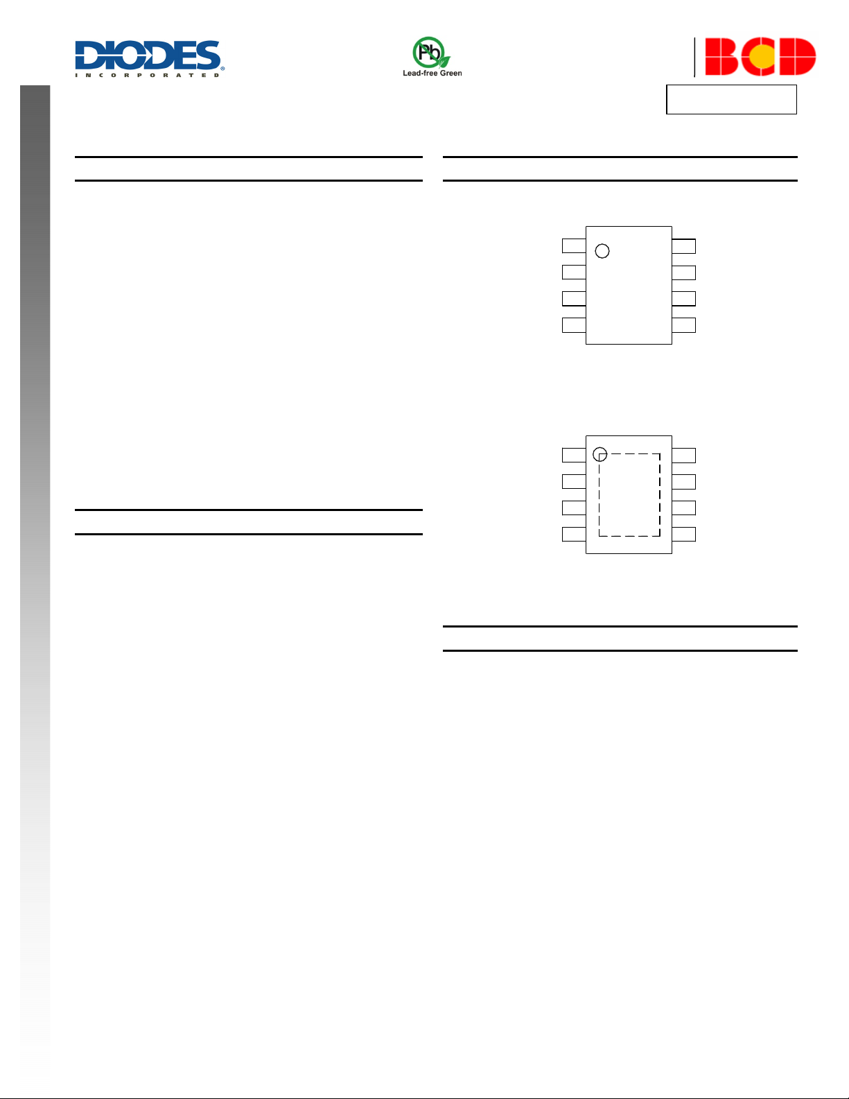
Pin Assignments
BOOT
UGATE
GND
LGATE/OCSET
(Top View)
1
2
3
4
8
PHASE
7
COMP/EN
6
FB
5
VCC
(SO-8/ M Package)
(Top View)
BOOT
UGATE
GND
LGATE/OCSET
1
2
3
4
Exposed
Pad
9
8
7
6
5
PHASE
COMP/EN
FB
VCC
(SO-8EP/ MP Package)
Applications
Subsystem Power Supplies
PCI, AGP, Graphics Cards, Digital TV
SSTL-2 and DDR/2/3 SDRAM Bus Termination Supply
Cable Modems, Set Top Boxes, and DSL Modems
Industrial Power Supplies and General Purpose Supplies
AP3585A/B/C
Document number: DS36819 Rev. 1 - 2
1 of 18
www.diodes.com
January 2014
© Diodes Incorporated
A
f
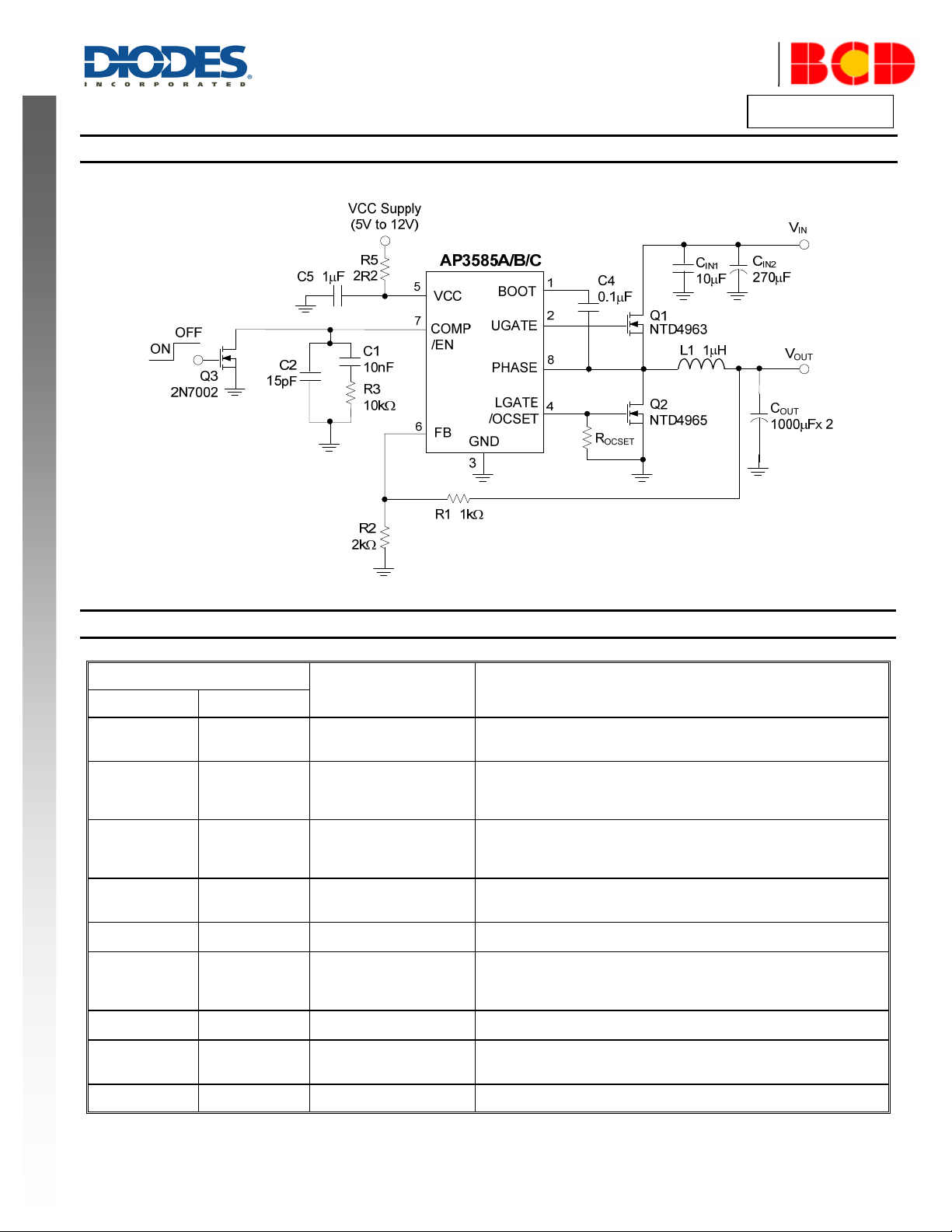
Typical Applications Circuit
Product Line o
Diodes Incorporated
AP3585A/B/C
NEW PRODUCT
Pin Descriptions
SO-8 SO-8EP
1 1 BOOT
2 2 UGATE
3 3 GND
4 4 LGATE/OCSET
5 5 VCC
6 6 FB
7 7 COMP/EN
8 8 PHASE
– 9 Exposed Pad
Pin Number
Pin Name Function
Bootstrap pin. Connect a bootstrap capacitor from this pin to PHASE for
creating a BOOT voltage suitable to drive a standard N-Channel
MOSFET.
Upper-gate drive pin. Connect this pin to the upper MOSFET gate
providing the gate drive. This pin is monitored by the adaptive shootthrough protection circuitry to determine when the upper MOSFET has
turned off.
Ground for the IC. All voltage levels are measured with respect to this pin.
Connect this pin directly to the low side MOSFET source and ground
plane with the lowest impedance. The exposed pad must be soldered to a
large PCB and connected to GND for maximum power dissipation.
Low-side Gate Driver Output and Over-Current Setting Input. This pin is
the gate driver for low-side MOSFET. It is also used to set the maximum
inductor current. Refer to the section in “Function Description” for detail.
Bias supply pin. Provides a 4.5V to 13.2V bias supply for the chip from this
pin. The pin should be bypassed with a capacitor to GND.
Feedback pin. This pin is the inverting input of the internal error amplifier.
Use FB pin, in combination with the COMP pin, to compensate the voltage
control feedback loop of the converter. A resistor divider from output to
GND is used to set the output voltage.
Compensation and disable pin. This pin is the output of the Error Amplifier.
Pull COMP pin low will shut down the IC.
This pin connects to the source of the upper MOSFET and the drain of the
lower MOSFET. This pin is also monitored by the adaptive shoot-through
protection circuitry to determine when the upper MOSFET has turned off.
Exposed Pad as ground pin.
AP3585A/B/C
Document number: DS36819 Rev. 1 - 2
2 of 18
www.diodes.com
January 2014
© Diodes Incorporated
A
f
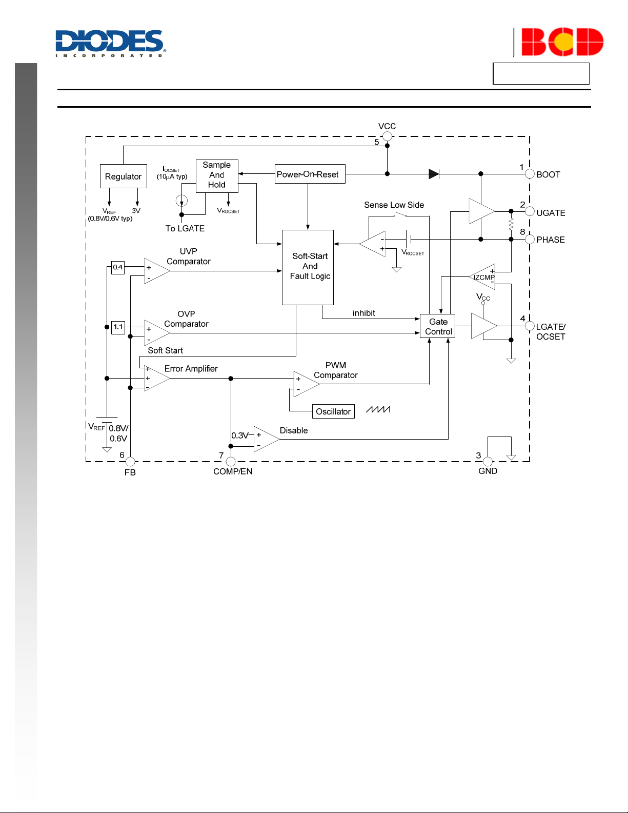
Functional Block Diagram
Product Line o
Diodes Incorporated
AP3585A/B/C
NEW PRODUCT
AP3585A/B/C
Document number: DS36819 Rev. 1 - 2
3 of 18
www.diodes.com
January 2014
© Diodes Incorporated
A
f
Product Line o
Diodes Incorporated
AP3585A/B/C
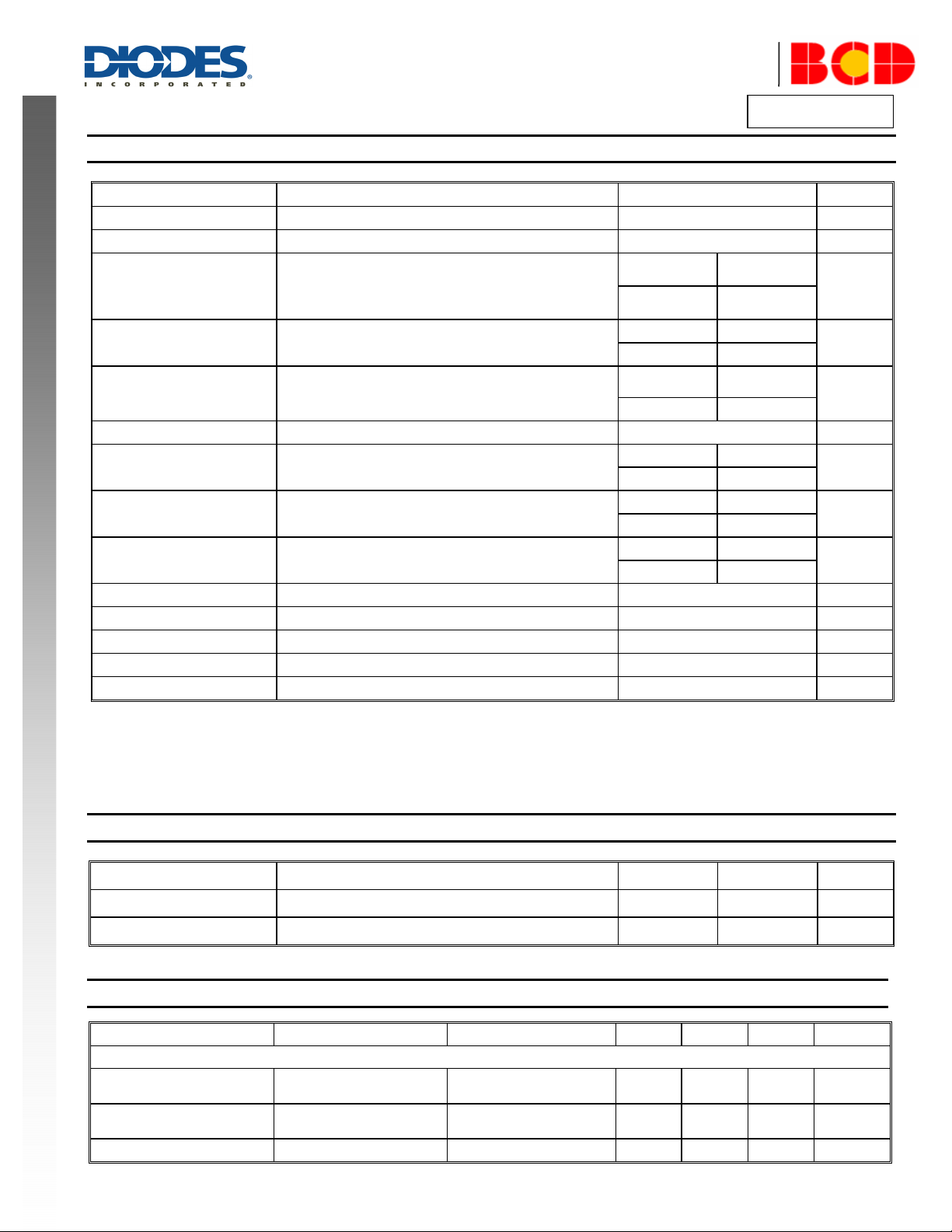
Absolute Maximum Ratings (Note 4)
Symbol Parameter
VCC
V
BOOT-PHASE
V
V
V
UGATE
PHASE
LGATE
Other Pin Voltage -0.3 to 6 V
PD
NEW PRODUCT
θJA
θJC
TJ
T
STG
T
LEAD
– ESD (Human Body Model) (Note 5) 2000 V
– ESD (Machine Model) (Note 5) 200 V
Notes: 4. Stresses greater than those listed under “Absolute Maximum Ratings” may cause permanent damage to the device. These are stress ratings only, and
5. Devices are ESD sensitive. Handling precaution is recommended.
functional operation of the device at these or any other conditions beyond those indicated under “Recommended Operating Conditions” is not implied.
Exposure to “Absolute Maximum Ratings” for extended periods may affect device reliability.
Supply Input Voltage -0.3 to 15 V
BOOT to PHASE Voltage -0.3 to 15 V
UGATE to PHASE Voltage
<200ns
PHASE to GND Voltage
LGATE to GND Voltage
Power Dissipation
Thermal Resistance (Junction to Ambient)
Thermal Resistance (Junction to Case)
Junction Temperature -40 to +150 ºC
Storage Temperature -65 to +150 ºC
Lead Temperature (Soldering, 10 sec) +260 ºC
<200ns -5 to 30
<200ns
SO-8EP 1.43
SO-8EP 70
SO-8EP 22
Rating
DC
DC -0.3 to 15
DC
SO-8 0.87
SO-8 115
SO-8 22
-0.3 to V
PHASE
-5 to V
PHASE
-0.3 to
V
CC
-5 to V
BOOT-
+0.3
BOOT-
+5
+0.3
CC
+5
Recommended Operating Conditions
Symbol Parameter Min Max Unit
VCC
Supply Input Voltage 4.5 13.2 V
Unit
V
V
V
W
ºC/W
ºC/W
TA
Operating Ambient Temperature -40 +85
C
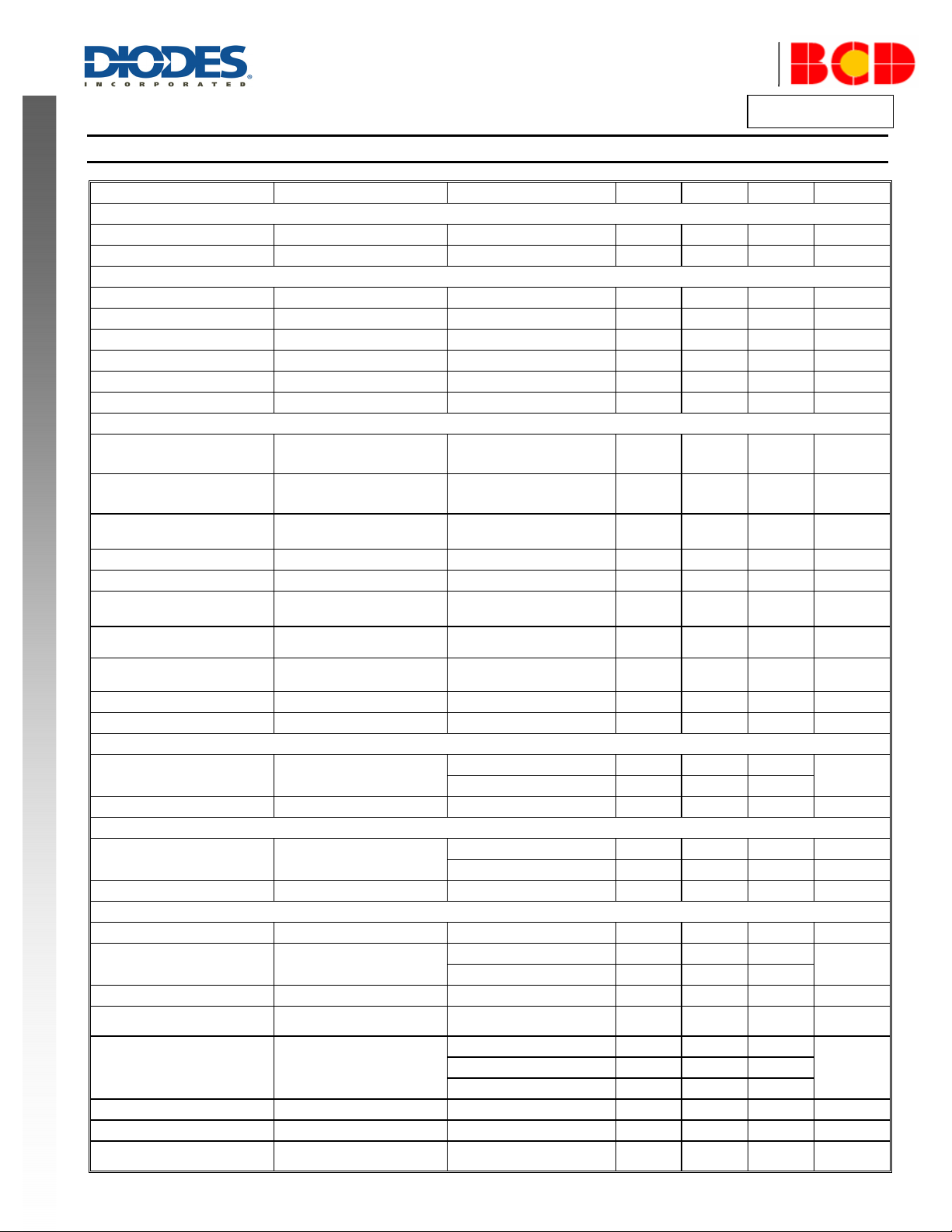
Electrical Characteristics (V
Symbol Parameter Conditions Min Typ Max Unit
SUPPLY INPUT
ICC
I
CC_Q
VIN
Supply Current
Quiescent Supply Current
Power Input Voltage – 3.0 – 13.2 V
= 12V, TA = +25oC, unless otherwise specified.)
CC
UGATE and LGATE Pins
Open; Switching
= V
REF
+0.1V,
V
FB
No Switching
– 5 – mA
– 4 – mA
AP3585A/B/C
Document number: DS36819 Rev. 1 - 2
4 of 18
www.diodes.com
January 2014
© Diodes Incorporated
A
f
Product Line o
Diodes Incorporated
AP3585A/B/C
Electrical Characteristics (Cont. V
= 12V, TA = +25oC, unless otherwise specified.)
CC
Symbol Parameter Conditions Min Typ Max Unit
POWER ON RESET
V
V
POR
V
V
POR_HYS
ERROR AMPLIFIER
G
DC_OL
GBW
SR Slew Rate – 3 6 – V/µs
– Transconductance – – 800 1100 µA/V
– Output Source Current
– Output Sink Current
PWM CONTROLLER GATE DRIVERS
I
UG_SRC
NEW PRODUCT
I
UG_SNK
R
UGATE
I
LG_SRC
I
LG_SNK
R
LGATE
–
–
– Minimum Duty Cycle – – 0 – %
– Maximum Duty Cycle – 75 82 89 %
OSCILLATOR
f
OSC
∆V
OSC
REFERENCE VOLTAGE
VFB
IFB
PROTECTION
V
FB_UVP
V
FB_OVP
I
OCSET
V
OCP_MAX
tSS
V
COMP/EN
T
OTSD
T
HYS
AP3585A/B/C
Document number: DS36819 Rev. 1 - 2
Rising Threshold VCC Rising
CC
Threshold Hysteresis
CC
–
4.0 4.2 4.4 V
– 500 – mV
Open Loop DC Gain – 55 70 – dB
Gain-bandwidth Product – – 10 – MHz
< V
REF
> V
REF
LGATE
= 6V
< 1.2V to V
< 1.2V to
= 5V
= 6V
= 12V,
= 6V
= 12V,
= 6V
LGATE
) > 1.2V
80 120 – µA
80 120 – µA
– -1.0 – A
– 1.5 – A
– 2 4 Ω
– -1 – A
– 1.5 – A
– 1 2 Ω
>
– 30 – ns
– 30 – ns
kHz
V
P-P
– 10 50 nA
0.3 0.4 0.5 V
V
9 10 11 µA
– 0.375 – V
V
FB
V
FB
V
Upper Gate Source Current
Upper Gate Sink Current
Upper Gate Sink
Resistance
Lower Gate Source Current
Lower Gate Sink Current
Lower Gate Sink
Resistance
PHASE Falling to LGATE
Rising Delay
LGATE Falling to UGATE
Rising Delay
Oscillator Frequency
BOOT-VPHASE
V
BOOT-VUGATE
V
BOOT-VPHASE
V
BOOT-VUGATE
50mA Source Current
VCC-V
V
LGATE
50mA Source Current
V
PHASE
1.2V
V
LGATE
(V
UGATE-VPHASE
AP3585A/B 270 300 330
AP3585C 180 200 220
Ramp Amplitude – – 1.4 –
Feedback Voltage
Feedback Bias Current
Under Voltage Protection
Over Voltage Protection
OC Current Source
Built-in Maximum OCP
Voltage
AP3585A 0.788 0.8 0.812 V
AP3585B/C 0.591 0.6 0.609 V
V
FB
–
AP3585A – 1.1 –
AP3585B/C – 0.8 –
–
–
AP3585A – 2 –
Soft-start Interval
Enable Threshold
Thermal Shutdown
Thermal Shutdown
Hysteresis
AP3585B – 1.5 –
AP3585C
–
–
–
– 2.4 –
0.25 0.30 0.35 V
– +160 – ºC
– +20 – ºC
5 of 18
www.diodes.com
ms
January 2014
© Diodes Incorporated
A
f
Product Line o
Diodes Incorporated
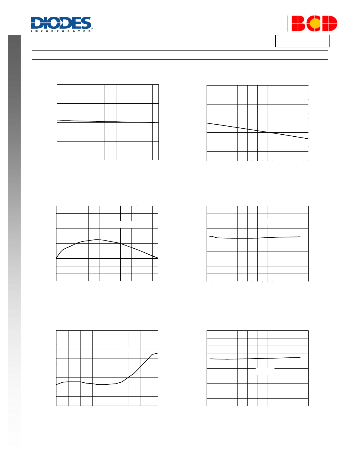
Performance Characteristics
Line Regulation Load Regulation
1.0
0.5
0.0
-0.5
Output Voltage Variation (%)
-1.0
5 6 7 8 9 10111213
NEW PRODUCT
Switching Frequency vs. Temperature Switching Frequency vs. Input Voltage
320
315
310
305
300
295
290
285
Switching Frequency (kHz)
280
275
270
-40-20 0 20406080100120140
Temperature (oC)
Reference Voltage vs. Temperature Reference Voltage vs. Input Voltage
0.816
0.814
0.812
0.810
0.808
0.806
Reference Voltage (V)
0.804
0.802
0.800
-40 -20 0 20 40 60 80 100 120
Temperature (oC)
Input Voltage (V)
AP3585A/B
V
AP3585A
OUT
=1.5V
4
3
2
1
0
-1
-2
Output Voltage Variation (%)
-3
-4
0 2 4 6 8 101214161820
320
315
310
305
300
295
290
285
Switching Frequency (kHz)
280
275
270
4 5 6 7 8 9 10 11 12 13 14
0.810
0.808
0.806
0.804
0.802
0.800
0.798
0.796
Reference Voltage (V)
0.794
0.792
0.790
4 5 6 7 8 9 10 11 12 13 14
Output Current (A)
AP3585A/B
Input Voltage (V)
AP3585A
Input Voltage (V)
AP3585A/B/C
V
=1.5V
OUT
AP3585A/B/C
Document number: DS36819 Rev. 1 - 2
6 of 18
www.diodes.com
January 2014
© Diodes Incorporated
 Loading...