Diodes AP3502E User Manual

340kHz, 2A Synchronous DC-DC Buck Converter AP3502E
Data Sheet
General Description
The AP3502E is a 340kHz fixed frequency, current
mode, PWM synchronous buck (step-down) DC-DC
converter, capable of driving a 2A load with high
efficiency, excellent line and load regulation. The
AP3502E exhibits high efficiency at light load. The
device integrates N-channel power MOSFET
switches with low on-resistance. Current mode
control provides fast transient response and
cycle-by-cycle current limit.
The AP3502E employs complete protection to ensure
system security. Including output Over Voltage
Protection, input Under Voltage Lock Out,
programmable Soft Start, Over Temperature
Protection and hiccup mode Short Circuit Protection.
This IC is available in SOIC-8 package.
Features
• Input Voltage Range: 4.5V to 18V
• Fixed 340kHz Frequency
• High Efficiency at Light Load
• High Efficiency: up to 95%
• Output Current: 2A
• Current Mode Control
• Built-in Over Current Protection
• Built-in Thermal Shutdown Function
• Built-in UVLO Function
• Built-in Over Voltage Protection
• Programmable Soft Start
• Hiccup Mode SCP
Applications
• LCD TV
• Set Top Box
• Portable DVD
• Digital Photo Frame
SOIC-8
Figure 1. Package Type of AP3502E
Dec. 2012 Rev. 1. 5 BCD Semiconductor Manufacturing Limited
1

Data Sheet
340kHz, 2A Synchronous DC-DC Buck Converter AP3502E
Pin Configuration
M Package
(SOIC-8)
BS
1
IN
SW
2
3
4
GND
Figure 2. Pin Configuration of AP3502E (Top View)
8
7
6
5
SS
EN
COMP
FB
Pin Description
Pin Number Pin Name Function
Bootstrap pin. A bootstrap capacitor is connected between the BS pin
1
2
3
4
5
6
7
8
BS
and SW pin. The voltage across the bootstrap capacitor drives the
internal high-side power MOSFET
IN
SW
Supply power input pin. A capacitor should be connected between the
IN pin and GND pin to keep the input voltage constant
Power switch output pin. This pin is connected to the inductor and
bootstrap capacitor
GND Ground pin
Feedback pin. This pin is connected to an external resistor divider to
program the system output voltage. When the FB pin voltage exceeds
FB
1.1V, the over voltage protection is triggered. When the FB pin
voltage is below 0.3V, the oscillator frequency is lowered to realize
short circuit protection
Compensation pin. This pin is the output of the transconductance
error amplifier and the input to the current comparator. It is used to
COMP
compensate the control loop. Connect a series RC network from this
pin to GND. In some cases, an additional capacitor from this pin to
GND pin is required
Control input pin. EN is a digital input that turns the regulator on or
EN
off. Drive EN high/low to turn on/off the regulator. Pull up with
100kΩ resistor for automatic startup
Soft-start control input pin. SS controls the soft-start period. Connect
SS
a capacitor from SS to GND to set the soft-start period. A 0.1μF
capacitor sets the soft-start period to 15ms. To disable the soft-start
feature, leave SS unconnected
Dec. 2012 Rev. 1. 5 BCD Semiconductor Manufacturing Limited
2

Data Sheet
340kHz, 2A Synchronous DC-DC Buck Converter AP3502E
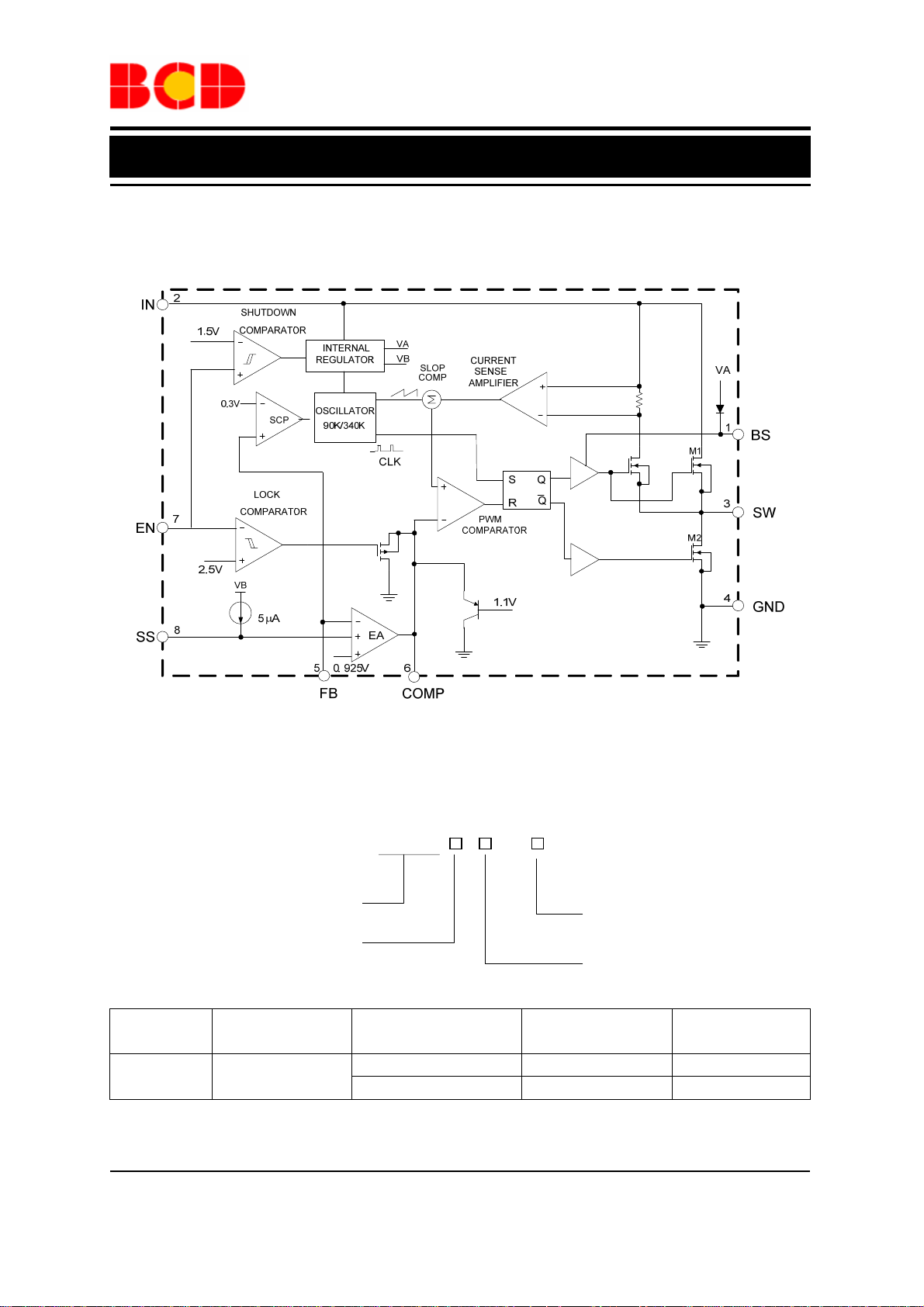
Functional Block Diagram
Figure 3. Functional Block Diagram of AP3502E
Ordering Information
AP3502E -
Circuit Type
Package
Package
SOIC-8
Temperature
M: SOIC-8
Range
-40 to 85°C
Part Number Marking ID Packing Type
AP3502EM-G1 3502EM-G1 Tube
AP3502EMTR-G1 3502EM-G1 Tape & Reel
BCD Semiconductor's Pb-free products, as designated with "G1" suffix in the part number, are RoHS compliant
and green.
G1: Green
TR: Tape & Reel
Blank: Tube
Dec. 2012 Rev. 1. 5 BCD Semiconductor Manufacturing Limited
3

Data Sheet
340kHz, 2A Synchronous DC-DC Buck Converter AP3502E
Absolute Maximum Ratings (Note 1)
Parameter Symbol Value Unit
IN Pin Voltage VIN -0.3 to 20 V
EN Pin Voltage VEN -0.3 to VIN V
SW Pin Voltage VSW 21 V
BS Pin Voltage VBS -0.3 to VSW+6 V
FB Pin Voltage VFB -0.3 to 6 V
COMP Pin Voltage V
SS Pin Voltage VSS -0.3 to 6 V
Thermal Resistance
Operating Junction Temperature TJ 150 ºC
Storage Temperature T
Lead Temperature (Soldering, 10sec) T
ESD (Human Body Model) V
ESD (Machine Model) VMM 200 V
Note 1: Stresses greater than those listed under “Absolute Maximum Ratings” may cause permanent damage to
the device. These are stress ratings only, and functional operation of the device at these or any other conditions
beyond those indicated under “Recommended Operating Conditions” is not implied. Exposure to “Absolute
Maximum Ratings” for extended periods may affect device reliability.
-0.3 to 6 V
COMP
θ
JA
-65 to 150 ºC
STG
260 ºC
LEAD
2000 V
HBM
105 ºC/W
Recommended Operating Conditions
Parameter Symbol Min Max Unit
Input Voltage VIN 4.5 18 V
Operating Ambient Temperature TA -40 85 ºC
Dec. 2012 Rev. 1. 5 BCD Semiconductor Manufacturing Limited
4
 Loading...