

Page 1
AP3440
Document number: DS36691 Rev. 2 - 2
1 of 15
www.diodes.com
March 2014
© Diodes Incorporated
AP3440
A Product Line of
Diodes Incorporated
NEW PRODUCT
Description
The AP3440 is a current mode, PWM synchronous buck (step-down)
DC-DC converter, capable of driving a 4A load with high efficiency,
excellent line and load regulation.
The device integrates two N-channel power MOSFETs with low onresistance. Current mode control provides fast transient response and
cycle-by-cycle current limit.
The switching frequency of AP3440 can be programmable from
200kHz to 2MHz, which allows small-sized components, such as
capacitors and inductors. A standard series of inductors from several
different manufacturers are available. This feature greatly simplifies
the design of switch-mode power supplies.
Under voltage lockout is internally set at 2.6V, but can be increased
by programming the threshold with a resistor network on the enable
pin. The output voltage startup ramp is controlled by the soft-start pin.
An open drain power good signal indicates the output is within 93% to
107% of its nominal voltage.
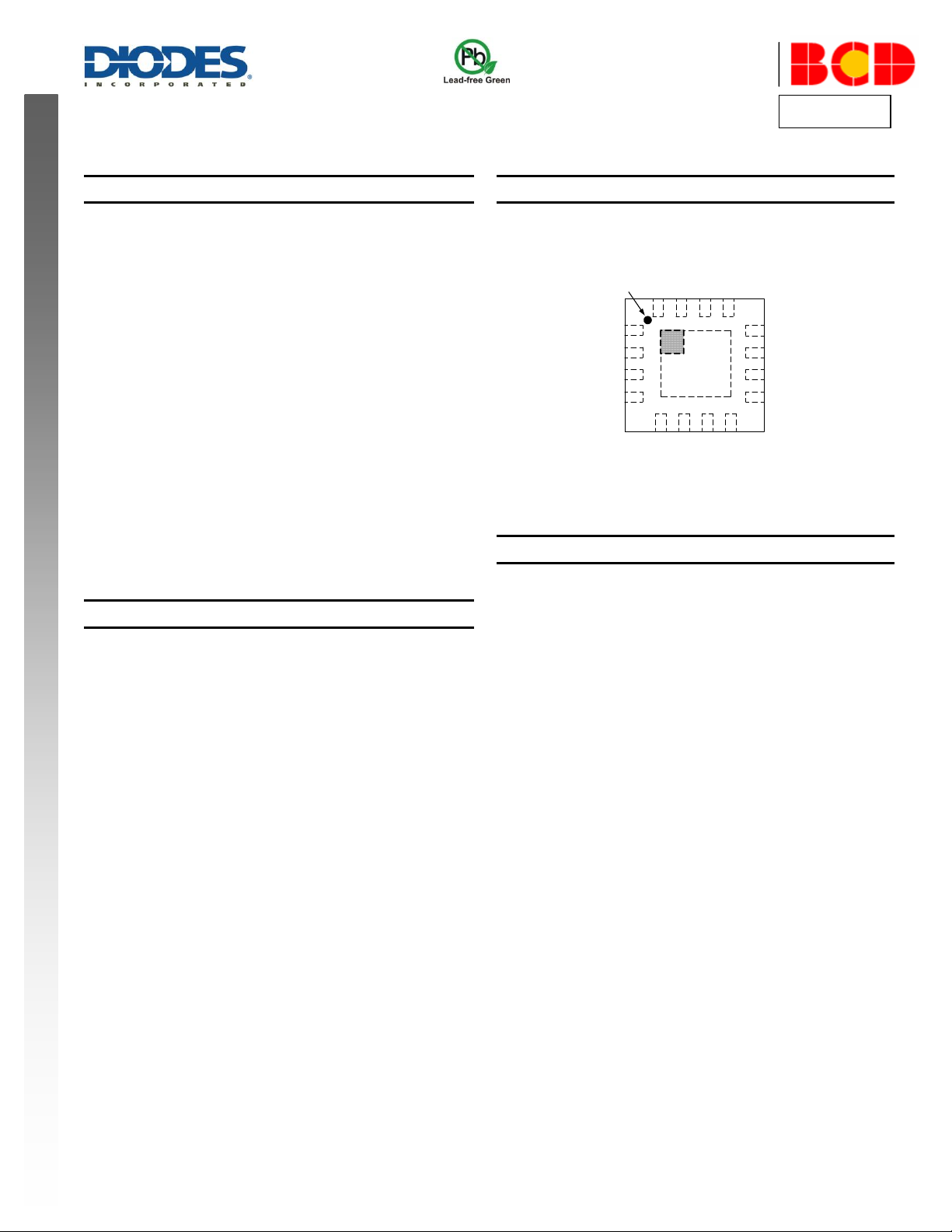
The AP3440 is available in U-QFN3030-16 package.
Applications
Low-voltage, High-density Power Systems
Point of Load Regulation for High Performance DSPs, FPGAs,
ASICs and Microprocessors
Broadband, Networking and Optical Communications
Infrastructure
Pin Assignments
(Top View)
VIN
VIN
GND
GND
AGND
FB
COMP
RT/CLK
SS
SW
SW
SW
BOOT
PGD
EN
VIN
E P
5 6 7 8
1
2
3
4 9
12
Pin 1 Mark
11
10
13141516
U-QFN3030-16
Features
Input Voltage Range: 2.95V to 5.5V
0.8V Reference Voltage with ±3% Precision
Two 30m(Typical) MOSFETs for High Efficiency at 4A Load
High Efficiency: Up to 94%
Output Current: 4A
Programmable Frequency:200kHz to 2MHz
Current Mode Control
Synchronizes to External Clock
Adjustable Soft-start
Soft Start-up into Pre-biased Output
UV and OV Power Good Output
Built-in Over Current Protection
Built-in Thermal Shutdown Function
Programmable UVLO Function
Built-in Over Voltage Protection
Thermally Enhanced 3mm×3mm 16-pin U-QFN3030-16
Totally Lead-free & Fully RoHS Compliant (Note1 & 2)
Halogen and Antimony Free. “Green” Device (Note 3)
4A, 2MHZ HIGH PERFORMANCE SYNCHRONOUS BUCK CONVERTER
Notes: 1. No purposely added lead. Fully EU Directive 2002/95/EC (RoHS) & 2011/65/EU (RoHS 2) compliant.
2. See http://www.diodes.com/quality/lead_free.html for more information about Diodes Incorporated’s definitions of Halogen- and Antimony-free, "Green"
and Lead-free.
3. Halogen- and Antimony-free "Green” products are defined as those which contain <900ppm bromine, <900ppm chlorine (<1500ppm total Br + Cl) and
<1000ppm antimony compounds.
Page 2
AP3440
Document number: DS36691 Rev. 2 - 2
2 of 15
www.diodes.com
March 2014
© Diodes Incorporated
AP3440
A Product Line of
Diodes Incorporated
NEW PRODUCT
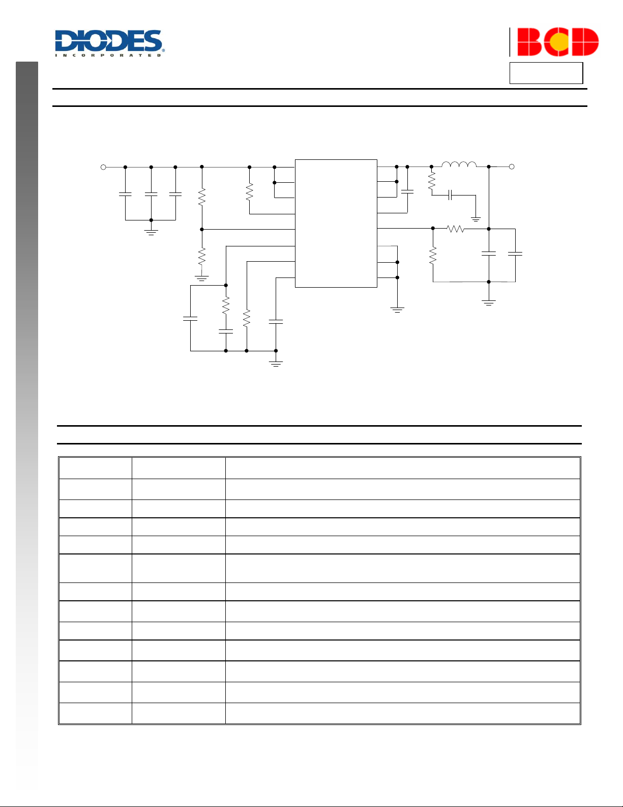
VIN
VIN
VIN
PGD
EN
COMP
SS
RT/CLK
SW
SW
SW
BOOT
FB
GND
GND
AGND
L1 1.5mH
V
OUT
=1.8V
R6 12.5kΩ
R7
10kΩ
VIN=5V
R4
100kΩ
16
1
2
14
15
7
8
9
10
11
12
13
6
4
5
3
C5
Optional
C2
C7
0.01mF
C4
2.7nF
R3
7.5kΩ
R5
180kΩ
R1
R2
AP3440
C3
C9
22mF
C1
10mF 0.1mF
C8
22mF
U1
C6
0.1mF
R8 2.2Ω
(Optional)
C10 2.2nF
(Optional)
Pin Number
Pin Name
Function
1,2,16
VIN
Supply input pin. A capacitor should be connected between the VIN and GND pin to keep the
DC input voltage constant
3,4
GND
Power ground. This pin should be electrically connected to the power pad under the IC
5
AGND
Analog ground. This pin should be electrically connected to GND close to the device
6
FB
Feedback pin. Inverting node of the transconductance error amplifier
7
COMP
Compensation pin. This pin is the output of the transconductance error amplifier and the input
to the current comparator. Connect external compensation elements to this pin to stabilize the
control loop
8
RT/CLK
Resistor timing or external clock input pin
9
SS
Soft-start pin. An external capacitor connected to this pin sets the output voltage rise time. This
pin can also be used for tracking
10,11,12
SW
Internal power switch output pin. This pin is connected to the inductor and bootstrap capacitor
13
BOOT
Bootstrap pin. A bootstrap capacitor is connected between the BOOT pin and SW pin. The
voltage across the bootstrap capacitor drives the internal high-side power MOSFET
14
PGD
Power good indicator output. Asserts low if output voltage is low due to thermal shutdown,
over-current, over/under-voltage or EN shut down
15
EN
Enable pin, internal pull-up current source. Pull below 1.2V to disable. Float to enable. Can be
used to set the on/off threshold (adjust UVLO) with two additional resistors
EP
Exposed Thermal Pad
Exposed Pad can be connected to GND, for best thermal performance thermal vias are
recommended under the package
Typical Applications Circuit
Pin Description
Page 3
AP3440
Document number: DS36691 Rev. 2 - 2
3 of 15
www.diodes.com
March 2014
© Diodes Incorporated
AP3440
A Product Line of
Diodes Incorporated
NEW PRODUCT
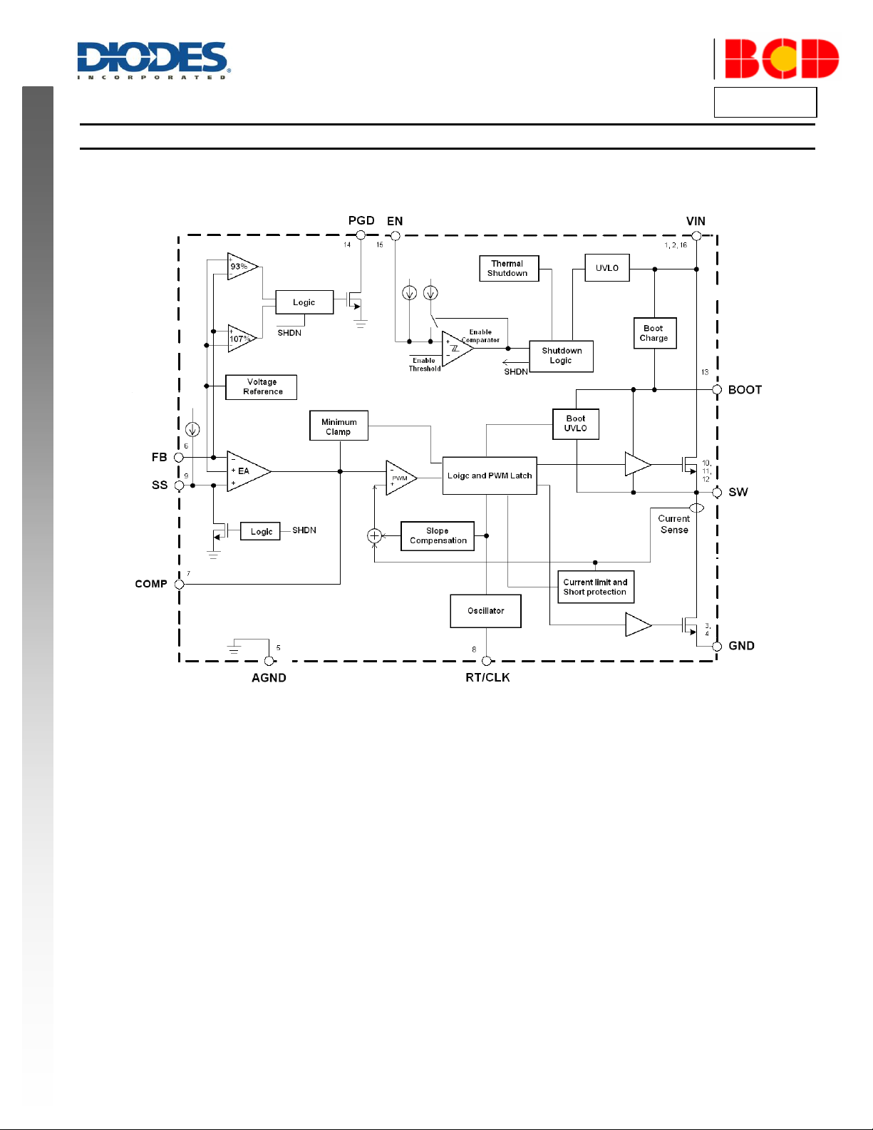
Functional Block Diagram
Page 4
AP3440
Document number: DS36691 Rev. 2 - 2
4 of 15
www.diodes.com
March 2014
© Diodes Incorporated
AP3440
A Product Line of
Diodes Incorporated
NEW PRODUCT
Symbol
Parameter
Rating
Unit
VIN
VIN Pin Voltage
-0.3 to 6.5
V
VEN
EN Pin Voltage
-0.3 to 6.5
V
VSW
SW Pin Voltage
-0.3 to VIN+0.3
V
VFB
FB Pin Voltage
-0.3 to 6.5
V
V
COMP
COMP Pin Voltage
-0.3 to 6.5
V
V
PGD
PGD Pin Voltage
-0.3 to 6.5
V
V
RT/CLK
RT/CLK Pin Voltage
-0.3 to 6.5
V
VSS
SS Pin Voltage
-0.3 to 6.5
V
JA
Thermal Resistance
70
ºC/W
TJ
Operating Junction Temperature
-40 to +125
ºC
T
STG
Storage Temperature
-65 to +150
ºC
T
LEAD
Lead Temperature (Soldering, 10sec)
+260
ºC
—
ESD(Machine Model)
200
V
—
ESD(Human Body Model)
2000
V
Symbol
Parameter
Min
Max
Unit
VIN
Input Voltage
2.95
5.5
V
I
OUT(MAX)
Maximum Output Current
4 — A
TA
Operating Ambient Temperature
-40
+85
ºC
Symbol
Parameters
Conditions
Min
Typ
Max
Unit
SUPPLY VOLTAGE (VIN PIN)
VIN
Input Voltage
—
2.95 — 5.5
V
IQ
Quiescent Current
VFB=0.9V, VIN=5V,
TA=+25ºC, RT=400k
—
360
575
μA
I
SHDN
Shutdown Supply Current
VEN=0V,TA=+25C,
2.95V≤V
IN
≤5.5V
—
2 5 μA
ENABLE AND UVLO (EN PIN)
V
EN_H
Enable Threshold
Rising
1.16
1.25
1.37
V
V
EN_L
Falling — 1.18 — V
V
UVLO
Internal Under Voltage
Lockout Threshold
—
—
2.6
2.8
V
V
HYS
Internal Under Voltage
Hysteresis
—
—
150 — mV
Absolute Maximum Ratings (Note 4)
Note 4: Stresses greater than those listed under “Absolute Maximum Ratings” may cause permanent damage to the device. These are stress ratings only, and
functional operation of the device at these or any other conditions beyond those indicated under “Recommended Operating Conditions” is not implied.
Exposure to “Absolute Maximum Ratings” for extended periods may affect device reliability.
Recommended Operating Conditions
Electrical Characteristics (@V
over full operating temperature range from -40 to +85ºC.)
=2.95 to 5.5V, TA=+25ºC, unless otherwise specified. Specifications with boldface type apply
IN
Page 5
AP3440
Document number: DS36691 Rev. 2 - 2
5 of 15
www.diodes.com
March 2014
© Diodes Incorporated
AP3440
A Product Line of
Diodes Incorporated
NEW PRODUCT
Symbol
Parameters
Conditions
Min
Typ
Max
Unit
VOLTAGE REFERENCE (FB PIN)
V
REF
Voltage Reference
2.95V≤V
IN
≤5.5V
0.779
0.803
0.827
V
MOSFET
R
ON_H
High Side Switch Onresistance
V
BOOT-SW
=5V
—
30
60
m
V
BOOT-SW
=2.95V
—
44
70
m
R
ON_L
Low Side Switch Onresistance
VIN=5V
—
30
60
m
VIN=2.95V
—
44
70
mΩ
CURRENT LIMIT
I
LIMIT
Current Limit Threshold
—
4.2
7.0 — A
THERMAL SHUTDOWN
T
TSD
Thermal Shutdown
—
—
140
—
C
—
Hysteresis
—
—
20
—
C
TIMING RESISTOR AND EXTERNAL CLOCK (RT/CLK PIN)
—
Switching Frequency Range
(RT Mode)
—
200 — 2000
kHz
—
Switching Frequency Range
(CLK Mode)
—
300 — 2000
kHz
fS
Switching Frequency
RT=400k
400
500
600
kHz
—
Minimum CLK Pulse Width
—
75
—
—
ns
—
RT/CLK Voltage
RT=400k
—
0.5 — V
—
RT/CLK High Threshold
—
—
1.6
2.2
V
—
RT/CLK Low Threshold
—
0.4
0.6 — V
BOOT (BOOT PIN)
R
BOOT
BOOT Charge Resistor
VIN=5V
—
16
— —
BOOT-SW UVLO
VIN=2.95V
—
2.2 — V
SOFT START (SS PIN)
ISS
Charge Current
VSS=0.4V
— 2 —
mA
VSS
SS to Reference Crossover
98% Nominal
—
1.1 — V
POWER GOOD (PGD PIN)
V
FB_TH
Feedback Threshold
VFB Falling (Fault)
—
91
—
%V
REF
VFB Rising (Good)
—
93
—
VFB Rising (Fault)
—
107
—
VFB Falling (Good)
—
105
—
Electrical Characteristics (Cont.) (@V
apply over full operating temperature range from -40 to +85ºC.)
=2.95 to 5.5V, TA=+25ºC, unless otherwise specified. Specifications with boldface type
IN
Page 6

AP3440
Document number: DS36691 Rev. 2 - 2
6 of 15
www.diodes.com
March 2014
© Diodes Incorporated
AP3440
A Product Line of
Diodes Incorporated
NEW PRODUCT
2.4 2.7 3.0 3.3 3.6 3.9 4.2 4.5 4.8 5.1 5.4 5.7
360
365
370
375
380
385
390
395
400
405
410
415
420
425
430
435
Supply Current (
mA)
Input Voltage (V)
-50 -25 0 25 50 75 100 125 150
390
395
400
405
410
415
420
425
430
435
440
445
450
455
460
Supply Current (
mA)
Temperature (oC)
-50 -25 0 25 50 75 100 125 150
2.10
2.15
2.20
2.25
2.30
2.35
2.40
2.45
2.50
2.55
2.60
UVLO Threshold (V)
Temperature (oC)
Start Switching
Stop Switching
-50 -25 0 25 50 75 100 125 150
1.14
1.15
1.16
1.17
1.18
1.19
1.20
1.21
1.22
1.23
1.24
1.25
1.26
1.27
1.28
EN Threshold (V)
Temperature (oC)
VIN=5V
Rising
Falling
0 300 600 900 1200 1500 1800 2100 2400 2700 3000 3300 3600 3900 4200
30
35
40
45
50
55
60
65
70
75
80
85
90
95
100
Efficiency (%)
Output Current (mA)
V
OUT
=1.8V
VIN=3.3V
VIN=5V
-50 -25 0 25 50 75 100 125 150
920
930
940
950
960
970
980
990
1000
1010
1020
RT=180k
Switching Frequency (kHz)
Temperature (oC)
Performance Characteristics
Supply Current vs. Input Voltage Supply Current vs. Temperature
UVLO Threshold vs. Temperature EN Threshold vs. Temperature
Efficiency vs. Output Current Switching Frequency vs. Temperature
Page 7

AP3440
Document number: DS36691 Rev. 2 - 2
7 of 15
www.diodes.com
March 2014
© Diodes Incorporated
AP3440
A Product Line of
Diodes Incorporated
NEW PRODUCT
V
OUT
1V/div
V
IN
2V/div
I
L
2A/div
VSS
2V/div
V
EN
2V/div
V
OUT
1V/div
VSS
2V/div
I
L
2A/div
V
OUT(AC)
200mV/div
I
OUT
2A/div
V
CLOCK
2V/div
VSW
2V/div
V
OUT
1V/div
VSS
2V/div
V
COMP
0.5V/div
I
L
2A/div
V
OUT
1V/div
VSS
2V/div
V
COMP
0.5V/div
I
L
2A/div
Performance Characteristics (Cont.)
Start Up from VIN (VIN=5V, V
OUT
=1.8V, I
=4A) Disable IC (VIN=5V, V
OUT
OUT
=1.8V, I
OUT
=4A)
Time 4ms/div Time 20ms/div
Load Transient Response (VIN=5V, V
OUT
=1.8V, I
=0 to 4A) Synchronizing to External Clock (f
OUT
CLOCK
=2MHz)
Time 200ms/div Time 400ns/div
Short Circuit Protection (VIN=5V, V
OUT
=1.8V, I
=4A) Short Circuit Recovery (VIN=5V, V
OUT
OUT
=1.8V, I
OUT
=4A)
Time 4ms/div Time 4ms/div
Page 8

AP3440
Document number: DS36691 Rev. 2 - 2
8 of 15
www.diodes.com
March 2014
© Diodes Incorporated
AP3440
A Product Line of
Diodes Incorporated
NEW PRODUCT
)(
)()(
)(
VV
AImst
nFC
REF
SSSS
SS
m
6
1059.2
944.0
1
STOPSTART
VV
R
6
102.3118.1
118.1
2
RV
R
R
STOP
AP3440
R1
R2
VIN
EN
2.55μA0.6μA
Application Note
Theory of Operation
The AP3440 consists of a reference voltage module, slope compensation circuit, error amplifier, PWM comparator, current limit circuit, two Nchannel MOSFETs etc. (Refer to the Functional Block Diagram on page 3 for detailed information)
Soft-start
The AP3440 integrates an internal soft start circuit to minimize inrush currents or provide power supply sequencing during power up. A capacitor
connected between SS pin and ground implements the soft-start time. The AP3440 has an internal pull-up current source of 2μA, which charges
the external slow start capacitor. Equation 1 calculates the required slow start capacitor, ISS is the internal slow start charging current of 2μA, and
V
is the internal voltage reference of 0.803V.
REF
………………….(1)
During normal operation, if the VIN goes below the UVLO, or the EN pin is pulled below 1.2V, or a thermal shutdown occurs, the AP3440 will stop
switching and the SS pin will be discharged to 40mV before reinitiating a powering up sequence.
Enable and Adjusting UVLO
The AP3440 are disabled when the VIN falls below 2.6V. If an application requires a higher under-voltage lockout (UVLO), use the EN pin as
shown in Figure 1 to adjust the input voltage UVLO by using two external resistors. The EN pin has an internal pull-up current source that provides
the default condition of the AP3440 operating when the EN pin floats. Once the EN pin voltage exceeds 1.25V, an additional 2.55μA of hysteresis
is added. When the EN pin is pulled below 1.18V, the 2.55μA hysteresis is removed. This additional current facilitates input voltage hysteresis.
For AP3440, the divider resistor R1 and R2 on the EN pin can be calculated according to equation 2 and 3.
…………………...(2)
………………(3)
Figure 1. Adjustable Under Voltage Lock Out
Adjusting Output Voltage
The output voltage is set with a resistor divider from the FB pin. It is recommended to use divider resistors with 1% tolerance or better. Start with a
10kΩ R2 resistor and use the equation 4 to calculate R1. To improve efficiency at very light loads consider using larger value resistors. If the
values are too high, the regulator is more susceptible to noise and voltage errors from the FB input current are noticeable.
Page 9

AP3440
Document number: DS36691 Rev. 2 - 2
9 of 15
www.diodes.com
March 2014
© Diodes Incorporated
AP3440
A Product Line of
Diodes Incorporated
NEW PRODUCT
1
803.0
21
OUT
V
RR
AP3440
R1
R2
V
OUT
FB
0.803V
SS
AP3440
R
T
RT/CLK
Clock
Source
Figure 3. Synchronizing to a System Clock
Figure 4. Synchronizing Waveform
0793.1
)(
311890
)(
kHzf
kR
SW
T
9393.0
)(
133870
)(
kR
kHzf
T
SW
Application Note (Cont.)
Resistor R1 can be calculated according to equation 4.
……………………….. (4)
Figure 2. Voltage Divider Circuit
Synchronize Using the RT/CLK Pin
The RT/CLK pin of AP3440 is used to synchronize the converter with an external system clock referring to Figure 3. To implement the
synchronization feature in a system, connect a square wave to the RT/CLK pin with an on-time of at least 75ns. When the clock is detected on the
RT/CLK pin, a mode change occurs and the pin becomes a synchronization input. The internal amplifier is disabled. If clocking edges stop, the
internal amplifier is re-enabled and the mode returns to the frequency set by the resistor. The low level of the square wave must be lower than
0.6V and the high level higher than 1.6V typically. The synchronization frequency range is from 300kHz to 2000kHz. The rising edge of the SW is
synchronized to the falling edge of RT/CLK pin. Figure 4 shows a typical synchronizing waveform, the clock frequency is 2MHz.
Constant Switching Frequency and Timing Resistor
The switching frequency of the AP3440 is adjustable over a wide range from 200kHz to 2000kHz by placing a resistor with maximum value of
1000kΩ and minimum of 85kΩ, respectively, on the RT/CLK pin. An internal amplifier holds this pin at a fixed voltage when connecting an external
resistor to ground to set the switching frequency. The V
use the equation 5.
To reduce the solution size one should typically set the switching frequency as high as possible, but tradeoffs of the efficiency, maximum input
voltage and minimum controllable on time should be considered.
……………………….(5)
………………………..(6)
is typically 0.5V. To determine the timing resistance for a given switching frequency,
RT/CLK
Page 10

AP3440
Document number: DS36691 Rev. 2 - 2
10 of 15
www.diodes.com
March 2014
© Diodes Incorporated
AP3440
A Product Line of
Diodes Incorporated
NEW PRODUCT
VIN
VIN
VIN
PGD
EN
COMP
SS
RT/CLK
SW
SW
SW
BOOT
FB
GND
GND
AGND
L1 1.5mH
V
OUT
=1.8V
R6 12.5kΩ
R7
10kΩ
VIN=5V
R4
100kΩ
16
1
2
14
15
7
8
9
10
11
12
13
6
4
5
3
C5
Optional
C2
C7
0.01mF
C4
2.7nF
R3
7.5kΩ
R5
180kΩ
R1
R2
AP3440
C3
C9
22mF
C1
Optional
10mF 0.1mF
C8
22mF
U1
C6
0.1mF
R8 2.2Ω
(Optional)
C10 2.2nF
(Optional)
IN
OUT
IN
OUT
OUT(MAX)CIN_RMS
V
V
1
V
V
II
Application Note (Cont.)
Over Current Protection
The AP3440 implements a cycle-by-cycle current limit. The high side switch current is detected during each cycle. During SCP conditions, V
pulled down and V
is drived to high, increasing the switch current. When the increased high side switch current is continuously detected to
COMP
trigger the current limit of high side switch 6 times, the high side and low side switches are turned off for about 2.5ms. Then both switches start
switching and they will not be turned off until the next 6 OCPs are triggered. The IC works with a hiccup mode during SCP conditions.
Power Good
The PGD pin output is an open drain MOSFET. The output is pulled low when the FB voltage enters the fault condition by falling below 91% or
rising above 107% of the nominal internal reference voltage. There is a 2% hysteresis on the threshold voltage, so when the FB voltage rises to
the good condition above 93% or falls below 105% of the internal voltage reference the PGD output MOSFET is turned off. It is recommended to
use a pull-up resistor between the values of 1kΩ Ω to a voltage source that is 5V or less. The PGD is in a valid state once the VIN input
voltage is greater than 1.2V.
Thermal Shutdown
The AP3440 implement an internal thermal shutdown to protect itself if the junction temperature exceeds +140°C. Switching is stopped when the
junction temperature exceeds the thermal trip threshold. Once the die temperature decreases below +120°C, the device reinitiates the soft start
operation. The thermal shutdown hysteresis is +20°C.
Component Selection
Typical application circuit of AP3440 is shown in Figure 5. For the major component selection please refer to the following section.
OUT
is
Input Capacitor
The AP3440 requires a high quality ceramic, type X5R or X7R, input decoupling capacitor of at least 4.7μF effective capacitance and in some
applications a bulk capacitor. The effective capacitance includes any DC bias effects. To ensure a stable operation, the input capacitor should be
placed as close to the VIN pin as possible, and its value varies according to different load and different characteristic of input impedance.
There are two important parameters of the input capacitor: the voltage rating and RMS current rating. The voltage rating of the input capacitor
should be at least 1.25 times larger than the maximum input voltage. The capacitor must also have a RMS current rating greater than the
maximum input current ripple of the AP3440. The RMS current of input capacitor can be expressed as:
Figure 5. Typical Application of AP3440
………..(7)
Page 11

AP3440
Document number: DS36691 Rev. 2 - 2
11 of 15
www.diodes.com
March 2014
© Diodes Incorporated
AP3440
A Product Line of
Diodes Incorporated
NEW PRODUCT
)
8
1
(
OUT
ESRLOUT
Cf
RIV
)(
kIVf
VV
VL
OUTIN
OUTIN
OUT
)
2
(
LVf
VV
VII
IN
OUTIN
OUTOUTPEAK
)(
)()(
)(
VV
AImst
nFC
REF
SSSS
SS
m
1
803.0
76
OUT
V
RR
Application Note (Cont.)
Output Capacitor
The output capacitor is the most critical component of a switching regulator. It is used for filtering output and keeping the loop stable. The typical
value is 44μF.
The primary parameters for output capacitor are the voltage rating and the equivalent series resistance (ESR). A low ESR capacitor is preferred to
keep the output voltage ripple low. The output ripple is calculated as the following:
……………..(8)
Where f is the switching frequency, C
Inductor
The inductor is used to supply smooth current to output when it is driven by a switching voltage. The higher the inductance, the lower the peak-topeak ripple current, as the higher inductance usually means the larger inductor size, so some trade-offs should be made when select an inductor.
The AP3440 is a synchronous buck converter. It always works on continuous current mode (CCM), and the inductor value can be selected as the
following:
is the output capacitance and △IL is the ripple current in the inductor.
OUT
…………………. ….(9)
Where V
to 40%. Another important parameter for the inductor is the current rating. Exceeding an inductor's maximum current rating may cause the
inductor to saturate and overheat. If inductor value has been selected, the peak inductor current can be calculated as the following:
It should be ensured that the current rating of the selected inductor is 1.5 times of the I
Slow Start Capacitor
The slow start capacitor determines the output voltage soft start time during power up.
The slow start capacitor value can be calculated using equation 11.
In AP3440, ISS is 2μA and V
Bootstrap Capacitor
A 0.1μF ceramic capacitor must be connected between the BOOT pin and the SW pin for normal operation. It is recommended to use a ceramic
capacitor with X5R or better grade dielectric.
Feedback Resistors
It is recommended to use divider resistors with 1% tolerance or better. Start with a 10kΩ for the R7 resistor and use the equation 12 to calculate
R6.
is the output voltage, VIN is the input voltage, I
OUT
…………..(10)
……………………… (11)
is 0.803V.
REF
…………………………………(12)
is the output current, k is the coefficient of ripple current, and its typical value is 20%
OUT
.
PEAK
Page 12

AP3440
Document number: DS36691 Rev. 2 - 2
12 of 15
www.diodes.com
March 2014
© Diodes Incorporated
AP3440
A Product Line of
Diodes Incorporated
NEW PRODUCT
OUTLOAD
P
CRf
2
1
1
OUTESR
Z
CRf
2
1
1
COMPEAOUT
P
CR
f
_
2
2
1
COMPCOMP
Z
CRf
2
1
2
Application Note (Cont.)
Compensation
The output capacitor and the load resistance largely determine where the error amplifier poles and zeros need to be placed for optimum transient
response and loop stability. The corner frequency of the pole and zero generated by output capacitor are:
………………………..(13)
………………………. .. (14)
Where R
The error amplifier provides most of the loop gain. After selecting the output capacitor, the control loop is compensated by tailoring the frequency
response of the error amplifier. The low frequency pole of the error amplifier is the dominant pole and is determined primarily by C
output resistance of the error amplifier as shown by:
is the load resistance, C
LOAD
is the output capacitance and R
OUT
…………………..(15)
is the capacitor ESR.
ESR
COMP
and the
Resistor R
Where R
A 7.5kΩ resistor and 2.7nF capacitor are used in typical application.
adds a zero to the frequency response to control gain in the mid frequency range. This zero frequency is:
COMP
……………………..(16)
COMP
and C
are compensation resistor and capacitor connected to COMP pin, R
COMP
is the output impedance of the error amplifier.
OUT_EA
Layout Consideration
PCB layout is very important to the performance of AP3440. The loop which switching current flows through should be kept as short as possible.
The external components (especially CIN) should be placed as close to the IC as possible.
The feedback trace should be routed far away from the inductor and noisy power traces, and it needs to be routed as direct as possible. Locate
the feedback divider resistor network near the feedback pin with short leads.
Since the SW connection is the switching node, the output inductor should be located very close to the SW pins, and the area of the PCB
conductor is minimized to prevent excessive capacitive coupling.
The boot capacitor must also be located close to the device. The sensitive analog ground connections for the feedback voltage divider,
compensation components, slow start capacitor and frequency set resistor should be connected to a separate analog ground trace.
The RT/CLK pin is sensitive to noise so the RT resistor should be located as close as possible to the IC and routed with minimal lengths of trace.
Figure 6. Top View of PCB Layout Figure 7. Bottom View of PCB Layout
Page 13

AP3440
Document number: DS36691 Rev. 2 - 2
13 of 15
www.diodes.com
March 2014
© Diodes Incorporated
AP3440
A Product Line of
Diodes Incorporated
NEW PRODUCT
AP3440 XX XX - XX
Packing
Package
TR : Tape & Reel
FN : U-QFN3030-16
G1 : Green
Product Name
RoHS/Green
Package
Temperature Range
Part Number
Marking ID
Packing
U-QFN3030-16
-40 to +85ºC
AP3440FNTR-G1
B2D
5000/Tape & Reel
B2D
YWW
MXX
: AAC Logo
B2D: Marking ID (Per Datasheet)
YWW: Year and Work Week of Mold Operation
M: Assembly Site Code
XX: The 7th & 8th Digits of Batch No.
· Pin 1 Mark
Ordering Information
Diodes IC’s Pb-free products with "G1" suffix in the part number, are RoHS compliant and green.
Marking Information
Page 14

AP3440
Document number: DS36691 Rev. 2 - 2
14 of 15
www.diodes.com
March 2014
© Diodes Incorporated
AP3440
A Product Line of
Diodes Incorporated
NEW PRODUCT
U-QFN3030-16
Type B
Dim
Min
Max
Typ
A
0.55
0.65
0.60
A1
0
0.05
0.02
A3
0.15
b
0.18
0.28
0.23
D
2.95
3.05
3.00
D2
1.40
1.60
1.50
E
2.95
3.05
3.00
E2
1.40
1.60
1.50
e
0.50
L
0.35
0.45
0.40
Z
0.625
All Dimensions in mm
Dimensions
Value
(in mm)
C
0.500
G
0.150
G1
0.150
X
0.350
X1
1.800
Y
0.600
Y1
1.800
Side View
A
A3
A1
Bottom View
D
D2
E
e
b (16x)
L (16x)
E2
(Pin #1 ID)
Z (8x)
0.450
R0.200
X (16x)
Y (16x)
C
Y1
X1
G1
G
Package Outline Dimensions
(1) Package Type: U-QFN3030-16
Suggested Pad Layout
(1) Package Type: U-QFN3030-16
Page 15

AP3440
Document number: DS36691 Rev. 2 - 2
15 of 15
www.diodes.com
March 2014
© Diodes Incorporated
AP3440
A Product Line of
Diodes Incorporated
NEW PRODUCT
DIODES INCORPORATED MAKES NO WARRANTY OF ANY KIND, EXPRESS OR IMPLIED, WITH REGARDS TO THIS DOCUMENT,
INCLUDING, BUT NOT LIMITED TO, THE IMPLIED WARRANTIES OF MERCHANTABILITY AND FITNESS FOR A PARTICULAR PURPOSE
(AND THEIR EQUIVALENTS UNDER THE LAWS OF ANY JURISDICTION).
Diodes Incorporated and its subsidiaries reserve the right to make modifications, enhancements, improvements, corrections or other changes
without further notice to this document and any product described herein. Diodes Incorporated does not assume any liability arising out of the
application or use of this document or any product described herein; neither does Diodes Incorporated convey any license under its patent or
trademark rights, nor the rights of others. Any Customer or user of this document or products described herein in such applications shall assume
all risks of such use and will agree to hold Diodes Incorporated and all the companies whose products are represented on Diodes Incorporated
website, harmless against all damages.
Diodes Incorporated does not warrant or accept any liability whatsoever in respect of any products purchased through unauthorized sales channel.
Should Customers purchase or use Diodes Incorporated products for any unintended or unauthorized application, Customers shall indemnify and
hold Diodes Incorporated and its representatives harmless against all claims, damages, expenses, and attorney fees arising out of, directly or
indirectly, any claim of personal injury or death associated with such unintended or unauthorized application.
Products described herein may be covered by one or more United States, international or foreign patents pending. Product names and markings
noted herein may also be covered by one or more United States, international or foreign trademarks.
This document is written in English but may be translated into multiple languages for reference. Only the English version of this document is the
final and determinative format released by Diodes Incorporated.
Diodes Incorporated products are specifically not authorized for use as critical components in life support devices or systems without the express
written approval of the Chief Executive Officer of Diodes Incorporated. As used herein:
A. Life support devices or systems are devices or systems which:
1. are intended to implant into the body, or
2. support or sustain life and whose failure to perform when properly used in accordance with instructions for use provided in the
labeling can be reasonably expected to result in significant injury to the user.
B. A critical component is any component in a life support device or system whose failure to perform can be reasonably expected to cause the
failure of the life support device or to affect its safety or effectiveness.
Customers represent that they have all necessary expertise in the safety and regulatory ramifications of their life support devices or systems, and
acknowledge and agree that they are solely responsible for all legal, regulatory and safety-related requirements concerning their products and any
use of Diodes Incorporated products in such safety-critical, life support devices or systems, notwithstanding any devices- or systems-related
information or support that may be provided by Diodes Incorporated. Further, Customers must fully indemnify Diodes Incorporated and its
representatives against any damages arising out of the use of Diodes Incorporated products in such safety-critical, life support devices or systems.
Copyright © 2014, Diodes Incorporated
www.diodes.com
IMPORTANT NOTICE
LIFE SUPPORT
 Loading...