Page 1
1.0MHz, 3.5A, Synchronous Step Down DC-DC Converter AP3435
Preliminary Datasheet
General Description
The AP3435 is a high efficiency step-down DC-DC
voltage converter. The chip operation is optimized
by peak-current mode architecture with built-in
synchronous power MOS switchers. The oscillator
and timing capacitors are all built-in providing an
internal switching frequency of 1MHz that allows
the use of small surface mount inductors and
capacitors for portable product implementations.
Integrated Soft Start (SS), Under Voltage Lock Out
(UVLO), Thermal Shutdown Detection (TSD) and
Short Circuit Protection are designed to provide
reliable product applications.
The device is available in adjustable output voltage
versions ranging from 0.8V to 0.9×V
(2.7V≤VIN≤5.5V), and is able to deliver up to 3.5A.
The AP3435 is available in PSOP-8 package.
Features
• High Efficiency Buck Power Converter
• Output Current: 3.5A
• Low R
• Adjustable Output Voltage from 0.8V to 0.9×V
• Wide Operating Voltage Range: 2.7V to 5.5V
•
Built-in Power Switches for Synchronous
Rectification with High Efficiency
• Feedback Voltage: 800mV
• 1.0MHz Constant Frequency Operation
• Thermal Shutdown Protection
• Low Drop-out Operation at 100% Duty Cycle
• No Schottky Diode Required
• Input Over Voltage Protection
Applications
IN
• LCD TV
• Set Top Box
• Post DC-DC Voltage Regulation
• PDA and Notebook Computer
Internal Switches:100mΩ (VIN=5V)
DS(ON)
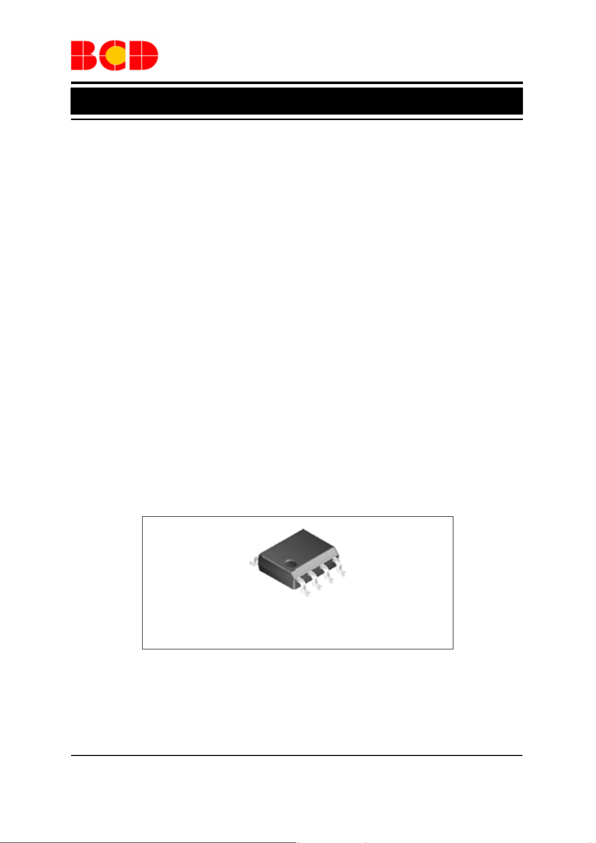
Figure 1. Package Type of AP3435
PSOP-8
IN
Dec. 2012 Rev. 1. 0 BCD Semiconductor Manufacturing Limited
1
Page 2
Preliminary Datasheet
1.0MHz, 3.5A, Synchronous Step Down DC-DC Converter AP3435
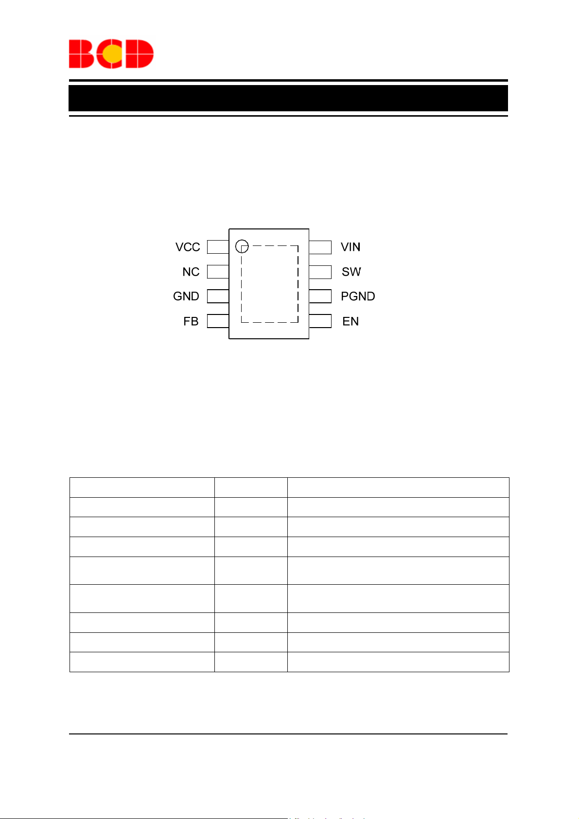
Pin Configuration
MP Package
(PSOP-8)
Pin Description
Pin Number Pin Name Function
1 VCC Supply input for the analog circuit
2 NC No connection
1
2
3
4
Figure 2. Pin Configuration of AP3435 (Top View)
8
7
6
5
3 GND Ground pin
4 FB
5 EN
6 PGND Power switch ground pin
7 SW Switch output pin
8 VIN Power supply input for the MOSFET switch
Feedback pin. Receive the feedback voltage from a
resistive divider connected across the output
Chip enable pin. Active high, internal pull-high with
200kΩ resistor
Dec. 2012 Rev. 1. 0 BCD Semiconductor Manufacturing Limited
2
Page 3
Preliminary Datasheet
1.0MHz, 3.5A, Synchronous Step Down DC-DC Converter AP3435
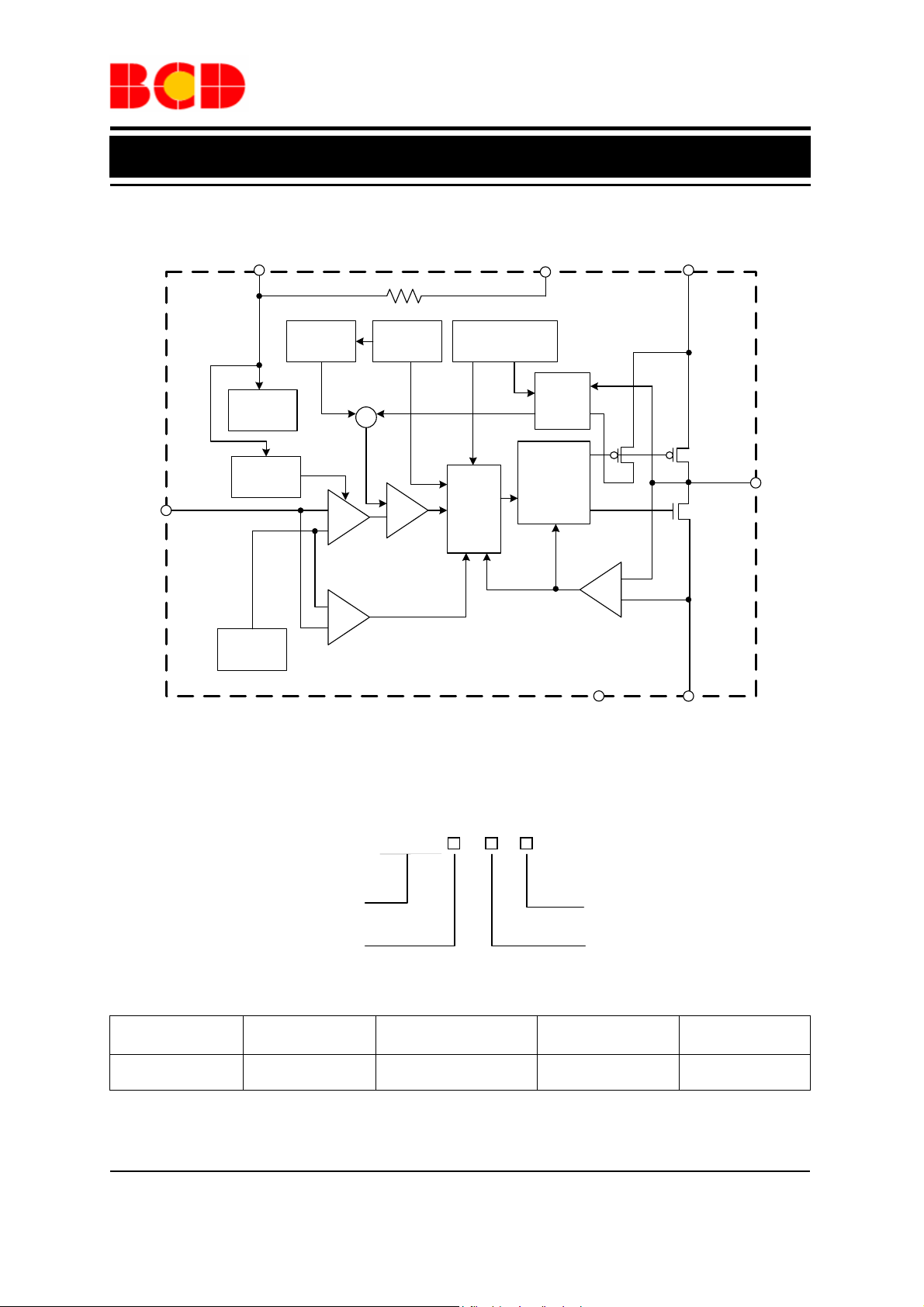
Functional Block Diagram
FB
EN
5
Saw-Tooth
Generator
Bias
Generator
Soft
Start
4
Bandgap
Reference
_
+
Error
Amplifier
_
+
Oscillator
+
+
_
Modulator
Over Voltage
Comparator
Over-Current
Comparator
Control
Logic
VCC
1
Current
Sensing
Buffer &
Dead Time
Control
Logic
_
+
Reverse Inductor
Current Comparator
3
VIN
8
6
7
SW
GND
Figure 3. Functional Block Diagram of AP3435
PGND
Ordering Information
AP3435 -
Circuit Type
Package
MP: PSOP-8
Package
Temperature
Range
Part Number Marking ID Packing Type
PSOP-8 -40 to 80°C AP3435MPTR-G1 3435MP-G1 Tape & Reel
BCD Semiconductor's Pb-free products, as designated with "G1" in the part number, are RoHS compliant and
green.
G1: Green
TR: Tape & Reel
Dec. 2012 Rev. 1. 0 BCD Semiconductor Manufacturing Limited
3
Page 4
Preliminary Datasheet
1.0MHz, 3.5A, Synchronous Step Down DC-DC Converter AP3435
Absolute Maximum Ratings (Note 1)
Parameter Symbol Value Unit
Supply Input for the Analog Circuit VCC
Power Supply Input for the MOSFET Switch VIN
SW Pin Switch Voltage VSW
Enable Input Voltage VEN
SW Pin Switch Current ISW
Power Dissipation (on PCB, TA=25°C)
Thermal Resistance (Junction to Ambient, Simulation)
Operating Junction Temperature TJ
Operating Temperature TOP
Storage Temperature T
ESD (Human Body Model) V
ESD (Machine Model) VMM
Note 1: Stresses greater than those listed under “Absolute Maximum Ratings” may cause permanent damage to
the device. These are stress ratings only, and functional operation of the device at these or any other conditions
beyond those indicated under “Recommended Operating Conditions” is not implied. Exposure to “Absolute
Maximum Ratings” for extended periods may affect device reliability.
PD 2.47 W
θJA 40.43 °C/W
STG
HBM
0 to 6.0
0 to 6.0
-0.3 to VIN+0.3
-0.3 to V
-40 to 85
-55 to 150
4.5
160
2000
200
IN
+0.3
V
V
V
V
A
°C
°C
°C
V
V
Recommended Operating Conditions
Parameter Symbol Min Max Unit
Supply Input Voltage VIN 2.7 5.5 V
Junction Temperature Range TJ -40 125 °C
Ambient Temperature Range TA -40 80 °C
Dec. 2012 Rev. 1. 0 BCD Semiconductor Manufacturing Limited
4
Page 5
Preliminary Datasheet
1.0MHz, 3.5A, Synchronous Step Down DC-DC Converter AP3435
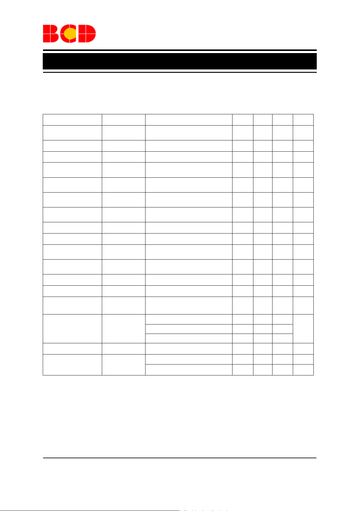
Electrical Characteristics
VIN=VCC=VEN=5V, V
specified.
Parameter Symbol Conditions Min Typ Max Unit
Input Voltage
Range
Shutdown Current I
Active Current ION V
Regulated Feedback
Voltage
Regulated Output
Voltage Accuracy
Peak Inductor
Current
Oscillator
Frequency
PMOSFET RON R
NMOSFET RON R
EN High-level Input
Voltage
EN Low-level Input
Voltage
EN Input Current
Soft Start Time
Maximum Duty
Cycle
Under Voltage Lock
Out Threshold
Thermal Shutdown TSD Hysteresis=30°C
Input Over Voltage
Protection (IOVP)
=1.2V, VFB=0.8V, L=2.2μH, CIN=10μF, C
OUT
ΔV
OUT/VOUT
V
V
D
V
IN
V
OFF
V
FB
4.5 A
I
PK
V
f
OSC
VIN=5V
ON(P)
VIN=5V
ON(N)
EN_H
EN_L
I
EN
t
SS
MAX
=0
EN
=0.95V
FB
For Adjustable Output Voltage
=2.7V to 5.5V,
V
IN
=0 to 3.5A
I
OUT
=2.7V to 5.5V
IN
1.5 V
0.4 V
1 μA
400 μs
100 %
2.7 5.5 V
Rising
V
UVLO
Falling
Hysteresis
Rising
V
IOVP
Hysteresis
=22μF, TA=25°C, unless otherwise
OUT
1 μA
310 μA
0.784 0.8 0.816 V
-3 3 %
1.0 MHz
100 mΩ
100 mΩ
2.4
2.3
0.1
150 °C
5.8 5.9 6.0 V
0.3 0.4 0.5 V
V
Dec. 2012 Rev. 1. 0 BCD Semiconductor Manufacturing Limited
5
Page 6
Preliminary Datasheet
1.0MHz, 3.5A, Synchronous Step Down DC-DC Converter AP3435
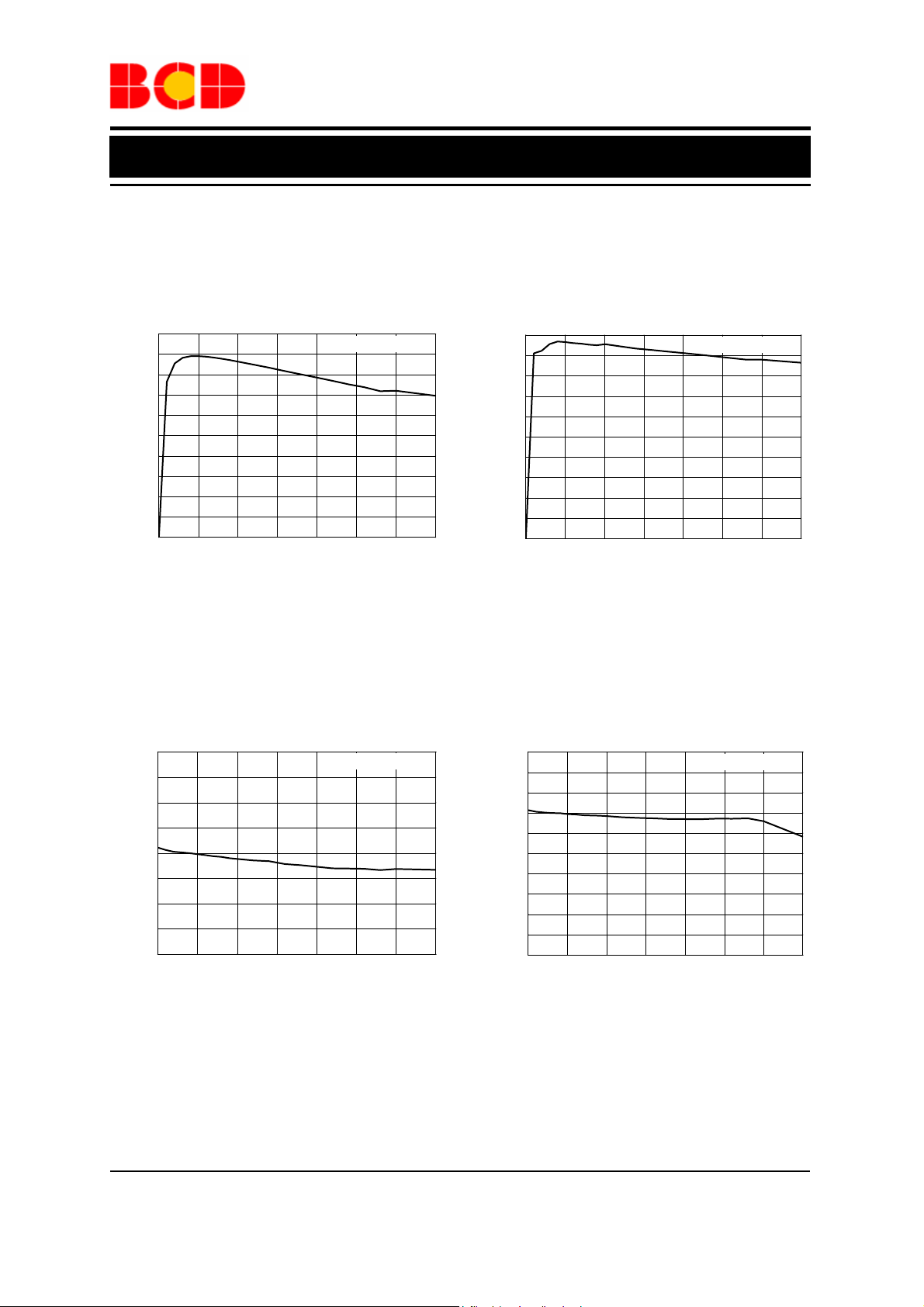
Typical Performance Characteristics
100
90
80
70
60
50
40
Efficiency (%)
30
20
10
0
0.0 0.5 1.0 1.5 2.0 2.5 3.0 3.5
Output Current (A)
VIN=5V, V
OUT
=1.2V
100
90
80
70
60
50
40
Efficiency (%)
30
20
10
0
0.0 0.5 1.0 1.5 2.0 2.5 3.0 3.5
Output Current (A)
VIN=5V, V
OUT
=3.3V
Figure 4. Efficiency vs. Output Current
Figure 5. Efficiency vs. Output Current
1.24
1.23
1.22
1.21
1.20
1.19
Output Voltage (V)
1.18
1.17
1.16
0.0 0.5 1.0 1.5 2.0 2.5 3.0 3.5
Output Current (A)
VIN=5V, V
OUT
=1.2V
3.40
3.38
3.36
3.34
3.32
3.30
3.28
Output Voltage (V)
3.26
3.24
3.22
3.20
0.0 0.5 1.0 1.5 2.0 2.5 3.0 3.5
Output Current (A)
VIN=5V, V
OUT
=3.3V
Figure 6. Load Regulation Figure 7. Load Regulation
Dec. 2012 Rev. 1. 0 BCD Semiconductor Manufacturing Limited
6
Page 7

Preliminary Datasheet
1.0MHz, 3.5A, Synchronous Step Down DC-DC Converter AP3435
Typical Performance Characteristics (Continued)
1.24
1.23
1.22
1.21
1.20
1.19
Output Voltage (V)
1.18
1.17
1.16
2.5 3.0 3.5 4.0 4.5 5.0 5.5
Input Voltage (V)
I
= 0
OUT
I
= 3.5A
OUT
V
=1.2V
OUT
Figure 8. Line Regulation Figure 9. Line Regulation
3.40
3.38
3.36
3.34
3.32
3.30
3.28
Output Voltage (V)
3.26
3.24
3.22
3.20
4.0 4.5 5.0 5.5
Input Voltage (V)
V
OUT
I
OUT
I
OUT
=3.3V
=0
=3.5A
1.20
1.15
1.10
1.05
1.00
0.95
Frequency (MHz)
0.90
0.85
0.80
2.5 3.0 3.5 4.0 4.5 5.0 5.5
Input Voltage (V)
V
= 1.2V
OUT
Figure 10. Frequency vs. Input Voltage Figure 11. Frequency vs. Input Voltage
Dec. 2012 Rev. 1. 0 BCD Semiconductor Manufacturing Limited
7
1.20
1.15
1.10
1.05
1.00
0.95
Frequency (MHz)
0.90
0.85
0.80
4.0 4.5 5.0 5.5
Input Voltage (V)
V
= 3.3V
OUT
Page 8

Preliminary Datasheet
1.0MHz, 3.5A, Synchronous Step Down DC-DC Converter AP3435
Typical Performance Characteristics (Continued)
1.5
1.4
1.3
1.2
1.1
1.0
0.9
0.8
0.7
EN Threshold Voltage (V)
0.6
0.5
0.4
2.5 3.0 3.5 4.0 4.5 5.0 5.5
Input Voltage (V)
H Level
L Level
4.6
4.4
4.2
4.0
3.8
Current Limit (A)
3.6
3.4
3.2
2.5 3.0 3.5 4.0 4.5 5.0 5.5
Input Voltage (V)
Figure 12. Enable Threshold Voltage vs. Input Voltage Figure 13. Current Limit vs. Input Voltage
90
85
80
75
C)
ο
70
65
60
55
50
45
Case Temperature (
40
35
30
25
0.00.51.01.52.02.53.03.5
Figure 14. Case Temperature vs. Output Current Figure 15.
(VIN=5V, VEN=0V to 5V, V
Output Current (A)
V
= 1.2V
OUT
V
EN
2V/div
V
OUT
1V/div
I
SW
2A/div
Time 400μs/div
Enable Waveform
OUT
=3.3V, I
OUT
=3.5A)
Dec. 2012 Rev. 1. 0 BCD Semiconductor Manufacturing Limited
8
Page 9

Preliminary Datasheet
1.0MHz, 3.5A, Synchronous Step Down DC-DC Converter AP3435
Typical Performance Characteristics (Continued)
V
V
IN
2V/div
2V/div
V
OUT
1V/div
IN
V
OUT
1V/div
2A/div
I
SW
I
SW
2A/div
Time 400μs/div
Time 20ms/div
Figure 16. Power-On Figure 17. Power-Off
(V
=0V to 5V, VEN=VIN, V
IN
OUT
=3.3V, I
=3.5A) (VIN=5V to 0V, VEN=VIN, V
OUT
OUT
=3.3V, I
OUT
=3.5A)
V
SW
2V/div
V
OUT
1V/div
V
SW
5V/div
V
OUT_AC
20mV/div
2A/div
Figure 18. Short Circuit Protection
=5V=VEN, V
(V
IN
Time 400μs/div
=3.3V, I
OUT
OUT
Figure 19. V
=2A to short) (VIN=5V=VEN, V
I
SW
2A/div
Time 400ns/div
Ripple
OUT
=3.3V, I
OUT
OUT
=0A)
I
OUT
Dec. 2012 Rev. 1. 0 BCD Semiconductor Manufacturing Limited
9
Page 10

Preliminary Datasheet
1.0MHz, 3.5A, Synchronous Step Down DC-DC Converter AP3435
Typical Performance Characteristics (Continued)
5V/div
VSW
V
SW
5V/div
V
V
OUT_AC
20mV/div
I
SW
2A/div
OUT_AC
20mV/div
I
2A/div
SW
Time 400ns/div
Time 400ns/div
Figure 20. V
=5V=VEN, V
(V
IN
Ripple Figure 21. V
OUT
OUT
=3.3V, I
=1A) (VIN=5V=VEN, V
OUT
OUT
Ripple
OUT
=3.3V, I
OUT
=3.5A)
V
OUT_AC
200mV/div
V
OUT_AC
200mV/div
I
OUT
500mA/div
I
OUT
500mA/div
Time 100μs/div
Time 100μs/div
(V
Figure 22. Load Transient of 1.2V Output Figure 23. Load Transient of 3.3V Output
=5V=VEN, V
IN
OUT
=1.2V, I
=0.5A to 2A) (VIN=5V=VEN, V
OUT
OUT
=3.3V, I
=0.5A to 2A)
OUT
Dec. 2012 Rev. 1. 0 BCD Semiconductor Manufacturing Limited
10
Page 11

Preliminary Datasheet
1.0MHz, 3.5A, Synchronous Step Down DC-DC Converter AP3435
Typical Performance Characteristics (Continued)
500mA/div
V
IN
1V/div
I
OUT
V
OUT
1V/div
V
1V/div
I
OUT
500mA/div
V
OUT
1V/div
IN
Time 100μs/div
Time 100μs/div
Figure 24. OVP Function (VIN=5V to 6V) Figure 25. Leave OVP Function (VIN=6V to 5V)
Dec. 2012 Rev. 1. 0 BCD Semiconductor Manufacturing Limited
11
Page 12

Preliminary Datasheet
1.0MHz, 3.5A, Synchronous Step Down DC-DC Converter AP3435
Application Information
The basic AP3435 application circuit is shown in Figure
27, external components selection is determined by the
load current and is critical with the selection of inductor
and capacitor values.
1. Inductor Selection
For most applications, the value of inductor is chosen
based on the required ripple current with the range of
1μH to 6.8μH.
I −
1
=Δ
V
OUTL
Lf
×
The largest ripple current occurs at the highest input
voltage. Having a small ripple current reduces the ESR
loss in the output capacitor and improves the efficiency.
The highest efficiency is realized at low operating
frequency with small ripple current. However, larger
value inductors will be required. A reasonable starting
point for ripple current setting is
maximum ripple current stays below a specified
value, the inductor should be chosen according to the
following equation:
L
=
V
[
OUT
MAXIf
Δ×
L
The DC current rating of the inductor should be at
least equal to the maximum output current plus half
the highest ripple current to prevent inductor core
saturation. For better efficiency, a lower
DC-resistance inductor should be selected.
2. Capacitor Selection
The input capacitance, CIN, is needed to filter the
trapezoidal current at the source of the top MOSFET.
To prevent large ripple voltage, a low ESR input
capacitor sized for the maximum RMS current must
be used. The maximum RMS capacitor current is
given by:
It indicates a maximum value at V
I
RMS=IOUT
commonly used for design because even significant
Dec. 2012 Rev. 1. 0 BCD Semiconductor Manufacturing Limited
II
×=
OMAXRMS
/2. This simple worse-case condition is
V
OUT
)1(
V
IN
△
IL=40%I
V
1][
)(
OUT
−
MAXV
IN
VVV
)]([ −
OUTINOUT
V
IN
=2V
IN
)(
1
2
MAX
]
, where
OUT
. For a
deviations do not much relieve. The selection of C
is determined by the Effective Series Resistance
(ESR) that is required to minimize output voltage
ripple and load step transients, as well as the amount
of bulk capacitor that is necessary to ensure that the
control loop is stable. The output ripple,
△
V
determined by:
[
ESRIV
LOUT
+Δ≤Δ
1
8
××
]
Cf
OUT
The output ripple is the highest at the maximum input
voltage since
△
IL increases with input voltage.
3. Load Transient
A switching regulator typically takes several cycles to
respond to the load current step. When a load step
occurs, V
△
to
I
resistance of output capacitor. △I
charge or discharge C
signal used by the regulator to return V
immediately shifts by an amount equal
OUT
×ESR, where ESR is the effective series
LOAD
also begins to
LOAD
generating a feedback error
OUT
OUT
steady-state value. During the recovery time, V
can be monitored for overshoot or ringing that would
indicate a stability problem.
4. Output Voltage Setting
The output voltage of AP3435 can be adjusted by a
resistive divider according to the following formula:
VV
REFOUT
R
1
R
2
V
The resistive divider senses the fraction of the output
voltage as shown in Figure 26.
FB
AP3435
GND
V
OUT
R1
R2
Figure 26. Setting the Output Voltage
12
R
1
+×=+×=
R
2
OUT
, is
OUT
to its
OUT
)1(8.0)1(
Page 13

+×=
Preliminary Datasheet
1.0MHz, 3.5A, Synchronous Step Down DC-DC Converter AP3435
Application Information (Continued)
5. Short Circuit Protection
When the AP3435 output node is shorted to GND, as
V
drops under 0.4V, the chip will enter soft-start
FB
mode to protect itself, when short circuit is removed,
and V
rises over 0.4V, the AP3435 recovers back to
FB
normal operation again. If the AP3435 reaches OCP
threshold while short circuit, the AP3435 will enter
soft-start cycle until the current under OCP threshold.
6.
Efficiency Considerations
The efficiency of switching regulator is equal to the
output power divided by the input power times 100%.
It is usually useful to analyze the individual losses to
determine what is limiting efficiency and which
change could produce the largest improvement.
Efficiency can be expressed as:
Efficiency=100%-L1-L2-…..
Where L1, L2, etc. are the individual losses as a
percentage of input power.
Although all dissipative elements in the regulator
produce losses, two major sources usually account for
most of the power losses: V
2
I
R losses. The VIN quiescent current loss dominates
the efficiency loss at very light load currents and the
2
I
R loss dominates the efficiency loss at medium to
heavy load currents.
6.1 The V
quiescent current loss comprises two
IN
parts: the DC bias current as given in the electrical
characteristics and the internal MOSFET switch gate
charge currents. The gate charge current results from
switching the gate capacitance of the internal power
MOSFET switches. Each cycle the gate is switched
from high to low, then to high again, and the packet
of charge, dQ moves from V
resulting dQ/dt is the current out of V
typically larger than the internal DC bias current. In
continuous mode,
QQfI +×=
Where Q
and QN are the gate charge of power
P
PMOSFET and NMOSFET switches. Both the DC
bias current and gate charge losses are proportional to
quiescent current and
IN
to ground. The
IN
)(
NPGATE
that is
IN
and this effect will be more serious at higher
the V
IN
input voltages.
2
6.2 I
R losses are calculated from internal switch
resistance, R
and external inductor resistance RL.
SW
In continuous mode, the average output current
flowing through the inductor is chopped between
power PMOSFET switch and NMOSFET switch.
Then, the series resistance looking into the SW pin is
a function of both PMOSFET R
R
resistance and the duty cycle (D):
DS(ON)
Therefore, to obtain the I
R
and multiply the result by the square of the
L
() ()
2
R losses, simply add RSW to
and NMOSFET
DS(ON)
−×
1
NONDSPONDSSW
average output current.
Other losses including C
and C
IN
ESR dissipative
OUT
losses and inductor core losses generally account for
less than 2 % of total additional loss.
7. Thermal Characteristics
In most applications, the part does not dissipate much
heat due to its high efficiency. However, in some
conditions when the part is operating in high ambient
temperature with high R
resistance and high
DS(ON)
duty cycles, such as in LDO mode, the heat
dissipated may exceed the maximum junction
temperature. To avoid the part from exceeding
maximum junction temperature, the user should do
some thermal analysis. The maximum power
dissipation depends on the layout of PCB, the thermal
resistance of IC package, the rate of surrounding
airflow and the temperature difference between
junction and ambient.
8. Input Over Voltage Protection
When input voltage of AP3435 is near 6V, the IC
will enter Input-Over-Voltage-Protection. It would be
shut down and there will be no output voltage in this
state. As the input voltage goes down below 5.5V, it
will leave input OVP and recover the output voltage.
)(
DRDRR
Dec. 2012 Rev. 1. 0 BCD Semiconductor Manufacturing Limited
13
Page 14

Preliminary Datasheet
1.0MHz, 3.5A, Synchronous Step Down DC-DC Converter AP3435
Application Information (Continued)
9. PCB Layout Considerations
When laying out the printed circuit board, the
following checklist should be used to optimize the
performance of AP3435.
1) The power traces, including the GND trace, the SW
trace and the VIN trace should be kept direct, short
and wide.
2) Put the input capacitor as close as possible to the
VIN and GND pins.
3) The FB pin should be connected directly to the
feedback resistor divider.
4) Keep the switching node, SW, away from the
sensitive FB pin and the node should be kept small
area.
Dec. 2012 Rev. 1. 0 BCD Semiconductor Manufacturing Limited
14
Page 15

Preliminary Datasheet
1.0MHz, 3.5A, Synchronous Step Down DC-DC Converter AP3435
Typical Application
Note 2:
AP3435
R
1
)1(
VV
REFOUT
+×= .
R
2
Figure 27. Typical Appl ication Circuit of AP3435
V
OUT
(V)
R1 (kΩ) R2 (kΩ)L (μH)
3.3 31.25 10 2.2
2.5 21.5 10 2.2
1.8 12.5 10 2.2
1.2 5 10 2.2
1.0 3 10 2.2
Table 1. Component Guide
Dec. 2012 Rev. 1. 0 BCD Semiconductor Manufacturing Limited
15
Page 16

Preliminary Datasheet
1.0MHz, 3.5A, Synchronous Step Down DC-DC Converter AP3435
Mechanical Dimensions
PSOP-8 Unit:mm(inch)
3.202(0.126)
3.402(0.134)
Dec. 2012 Rev. 1. 0 BCD Semiconductor Manufacturing Limited
16
Page 17

BCD Semiconductor Manufacturing Limited
IMPORTANT NOTICE
IMPORTANT NOTICE
BCD Semiconductor Manufacturing Limited reserves the right to make changes without further notice to any products or specifi-
BCD Semiconductor Manufacturing Limited reserves the right to make changes without further notice to any products or specifi-
cations herein. BCD Semiconductor Manufacturing Limited does not assume any responsibility for use of any its products for any
cations herein. BCD Semiconductor Manufacturing Limited does not assume any responsibility for use of any its products for any
particular purpose, nor does BCD Semiconductor Manufacturing Limited assume any liability arising out of the application or use
particular purpose, nor does BCD Semiconductor Manufacturing Limited assume any liability arising out of the application or use
of any its products or circuits. BCD Semiconductor Manufacturing Limited does not convey any license under its patent rights or
of any its products or circuits. BCD Semiconductor Manufacturing Limited does not convey any license under its patent rights or
other rights nor the rights of others.
other rights nor the rights of others.
http://www.bcdsemi.com
MAIN SITE
MAIN SITE
- Headquarters
BCD Semiconductor Manufacturing Limited
BCD Semiconductor Manufactur ing Limited
- Wafer Fab
No. 1600, Zi Xing Road, Shanghai ZiZhu Science-based Industrial Park, 200241, China
Shanghai SIM-BCD Semiconductor Manufacturing Limited
Tel: +86-21-24162266, Fax: +86-21-24162277
800, Yi Shan Road, Shanghai 200233, China
Tel: +86-21-6485 1491, Fax: +86-21-5450 0008
REGIONAL SALES OFFICE
Shenzhen Office
REGIONAL SALES OFFICE
Shanghai SIM-BCD Semiconductor Manufacturing Co., Ltd., Shenzhen Office
Shenzhen Office
Unit A Room 1203, Skyworth Bldg., Gaoxin Ave.1.S., Nanshan District, Shenzhen,
Shanghai SIM-BCD Semiconductor Manufacturing Co., Ltd. Shenzhen Office
China
Advanced Analog Circuits (Shanghai) Corporation Shenzhen Office
Tel: +86-755-8826 7951
Room E, 5F, Noble Center, No.1006, 3rd Fuzhong Road, Futian District, Shenzhen 518026, China
Fax: +86-755-8826 7865
Tel: +86-755-8826 7951
Fax: +86-755-8826 7865
- Wafer Fab
BCD Semiconductor Manufacturing Limited
Shanghai SIM-BCD Semiconductor Manufacturing Co., Ltd.
- IC Design Group
800 Yi Shan Road, Shanghai 200233, China
Advanced Analog Circuits (Shanghai) Corporation
Tel: +86-21-6485 1491, Fax: +86-21-5450 0008
8F, Zone B, 900, Yi Shan Road, Shanghai 200233, China
Tel: +86-21-6495 9539, Fax: +86-21-6485 9673
Taiwan Office
BCD Semiconductor (Taiwan) Company Limited
Taiwan Office
4F, 298-1, Rui Guang Road, Nei-Hu District, Taipei,
BCD Semiconductor (Taiwan) Company Limited
Tai wan
4F, 298-1, Rui Guang Road, Nei-Hu District, Taipei,
Tel: +886-2-2656 2808
Taiwan
Fax: +886-2-2656 2806
Tel: +886-2-2656 2808
Fax: +886-2-2656 2806
USA Office
BCD Semiconductor Corp.
USA Office
30920 Huntwood Ave. Hayward,
BCD Semiconductor Corporation
CA 94544, USA
30920 Huntwood Ave. Hayward,
Tel : +1-510-324-2988
CA 94544, U.S.A
Fax: +1-510-324-2788
Tel : +1-510-324-2988
Fax: +1-510-324-2788
 Loading...