

Page 1
3A, 2MHz High Performance Synchronous Buck Converter AP3433
Preliminary Datasheet
General Description
The AP3433 is a current mode, PWM synchronous
buck (step-down) DC-DC converter, capable of
driving a 3A load with high efficiency, excellent line
and load regulation.
The device integrates two N-channel power
MOSFETs with low on-resistance. Current mode
control provides fast transient response and
cycle-by-cycle current limit.
The switching frequency of AP3433 can be
programmable from 300kHz to 2MHz, which allows
small-sized components, such as capacitors and
inductors. A standard series of inductors from several
different manufacturers are available. This feature
greatly simplifies the design of switch-mode power
supplies.
Under voltage lockout is internally set at 2.6V, but
can be increased by programming the threshold with
a resistor network on the enable pin. The output
voltage startup ramp is controlled by the soft-start pin.
An open drain power good signal indicates the output
is within 93% to 107% of its nominal voltage.
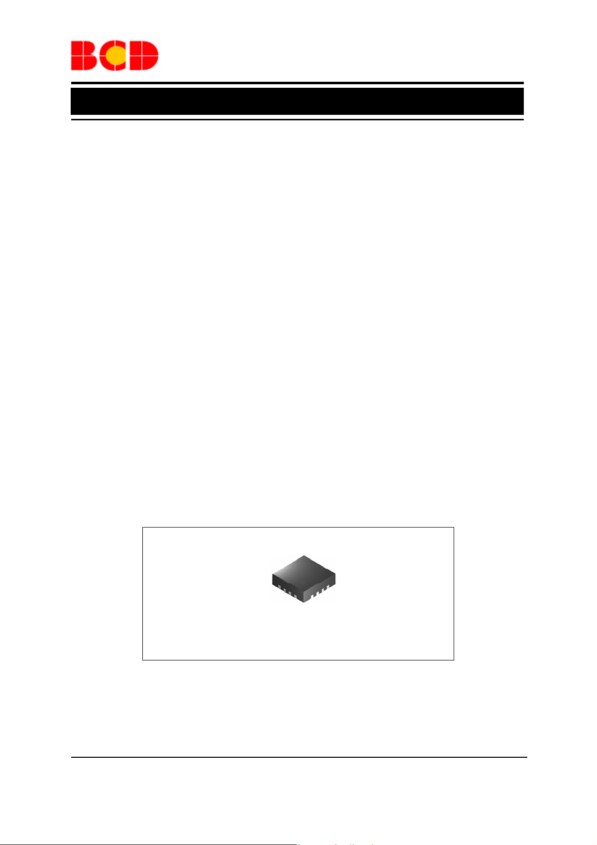
The AP3433 is available in QFN-3×3-16 package.
Features
• Input Voltage Range: 2.95V to 5.5V
• 0.827V Reference Voltage with ±3% Precision
• Two 45mΩ(typical) MOSFETs for High
Efficiency at 3A Load
• High Efficiency: up to 94%
• Output Current: 3A
• Programmable Frequency:300kHz to 2MHz
• Current Mode Control
• Synchronizes to External Clock
• Adjustable Soft-start
• Soft Start-up into Pre-biased Output
• UV and OV Power Good Output
• Built-in Over Current Protection
• Built-in Thermal Shutdown Function
• Programmable UVLO Function
• Built-in Over Voltage Protection
• Thermally Enhanced 3mm×3mm 16-pin QFN
Applications
• Low-voltage, High-density Power Systems
• Point of Load Regulation for Consumer
Applications such as Set Top Boxes, LCD
Displays, CPE Equipment
QFN-3×3-16
Figure 1. Package Type of AP3433
Jul. 2012 Rev. 1. 1 BCD Semiconductor Manufacturing Limited
1
Page 2
Preliminary Datasheet
3A, 2MHz High Performance Synchronous Buck Converter AP3433
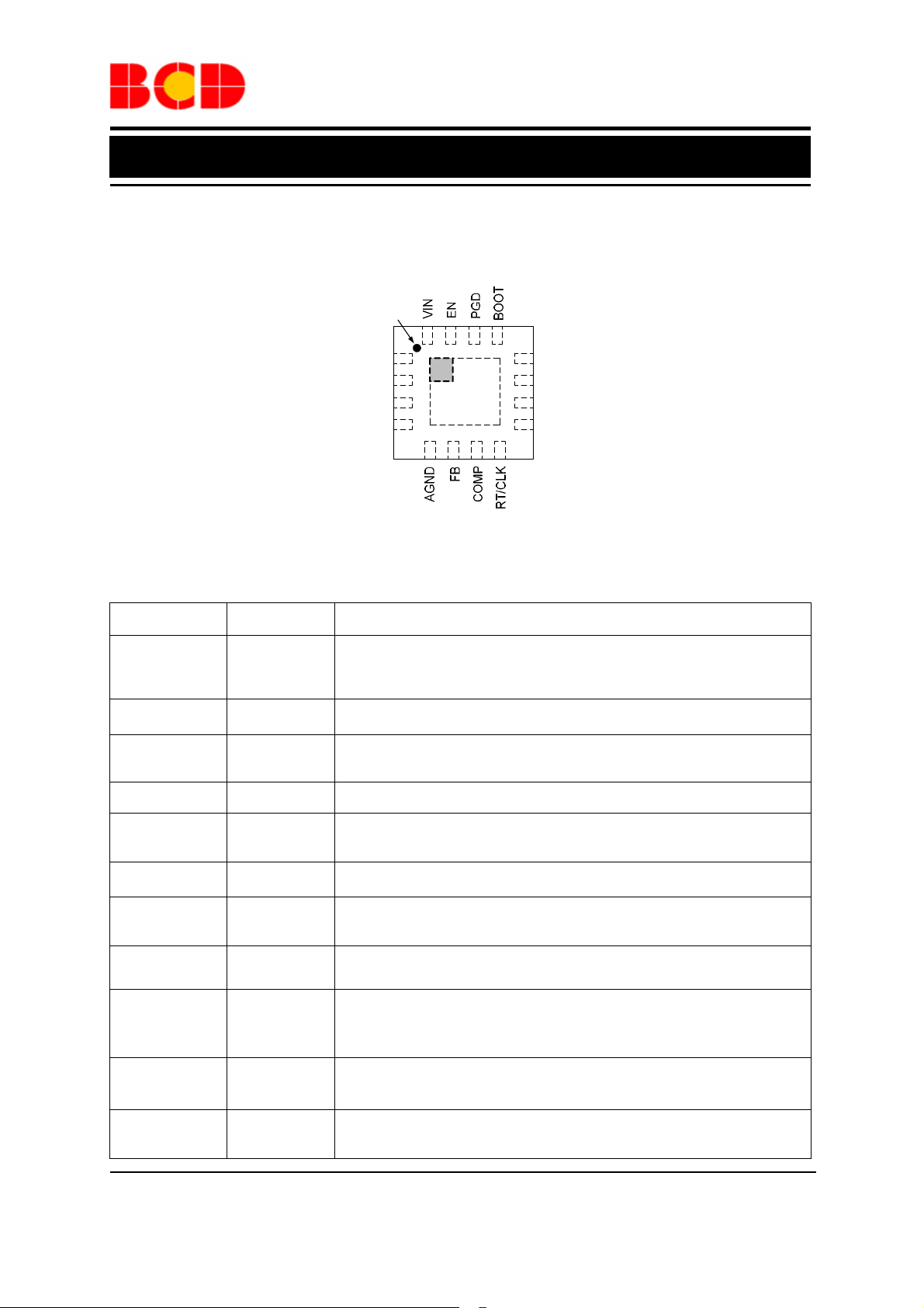
Pin Configuration
FN Package
(QFN-3×3-16)
Pin 1 Mark
13141516
VIN
1
2
VIN
GND
3
49
GND
EP
5678
SW
12
SW
11
SW
10
SS
Figure 2. Pin Configuration of AP3433 (Top View)
Pin Description
Pin Number Pin Name Function
1,2,16 VIN
3,4 GND
5 AGND
6 FB Feedback pin. Inverting node of the transconductance error amplifier
7 COMP
8 RT/CLK Resistor timing or external clock input pin
9 SS
10,11,12 SW
Supply input pin. A capacitor should be connected between the VIN and GND
pin to keep the DC input voltage constant
Power ground. This pin should be electrically connected to the power pad under
the IC
Analog ground. This pin should be electrically connected to GND close to the
device
Compensation pin. This pin is the output of the transconductance error amplifier
and the input to the current comparator. Connect external compensation elements
to this pin to stabilize the control loop
Soft-start pin. An external capacitor connected to this pin sets the output voltage
rise time. This pin can also be used for tracking
Internal power switch output pin. This pin is connected to the inductor and
bootstrap capacitor
Bootstrap pin. A bootstrap capacitor is connected between the BOOT pin and SW
13 BOOT
pin. The voltage across the bootstrap capacitor drives the internal high-side power
MOSFET
14 PGD
Power good indicator output. Asserts low if output voltage is low due to thermal
shutdown, over-current, over/under-voltage or EN shut down
Enable pin, internal pull-up current source. Pull below 1.2V to disable. Float to
15 EN
enable. Can be used to set the on/off threshold (adjust UVLO) with two additional
resistors
Jul. 2012 Rev. 1. 1 BCD Semiconductor Manufacturing Limited
2
Page 3
Preliminary Datasheet
3A, 2MHz High Performance Synchronous Buck Converter AP3433
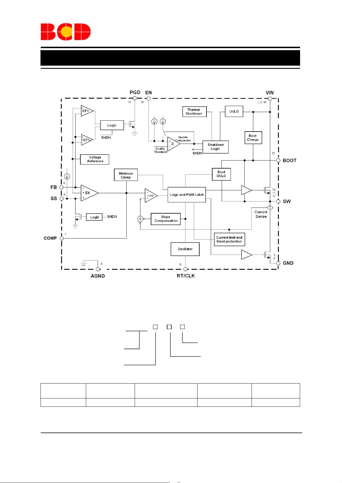
Functional Block Diagram
Figure 3. Functional Block Diagram of AP3433
Ordering Information
AP3433 -
Circuit Type
Package
FN: QFN-3
Package
QFN-3×3-16 -40 to 85ºC AP3433FNTR-G1 B1D Tape & Reel
Temperature
×3-16
Range
Part Number Marking ID Packing Type
BCD Semiconductor's Pb-free products, as designated with "G1" suffix in the part number, are RoHS compliant
and green.
Jul. 2012 Rev. 1. 1 BCD Semiconductor Manufacturing Limited
3
G1: Green
TR: Tape & Reel
Page 4

Preliminary Datasheet
3A, 2MHz High Performance Synchronous Buck Converter AP3433
Absolute Maximum Ratings (Note 1)
Parameter Symbol Value Unit
VIN Pin Voltage VIN -0.3 to 6.5 V
EN Pin Voltage VEN -0.3 to 6.5 V
SW Pin Voltage VSW -0.3 to VIN+0.3 V
FB Pin Voltage VFB -0.3 to 6.5 V
COMP Pin Voltage V
PGD Pin Voltage V
RT/CLK Pin Voltage V
SS Pin Voltage VSS -0.3 to 6.5 V
Thermal Resistance
(Junction to Ambient)
Thermal Resistance
(Junction to Case)
Operating Junction Temperature TJ -40 to 125 ºC
Storage Temperature T
Lead Temperature (Soldering, 10sec) T
ESD (Machine Model) 200 V
ESD (Human Body Model) 2000 V
θ
JC (BOTTOM)
-0.3 to 6.5 V
COMP
-0.3 to 6.5 V
PGD
-0.3 to 6.5 V
RT/ CLK
θ
JA
-65 to 150 ºC
STG
260 ºC
LEAD
70 ºC/W
5 ºC/W
Note 1: Stresses greater than those listed under “Absolute Maximum Ratings” may cause permanent damage to
the device. These are stress ratings only, and functional operation of the device at these or any other conditions
beyond those indicated under “Recommended Operating Conditions” is not implied. Exposure to “Absolute
Maximum Ratings” for extended periods may affect device reliability.
Recommended Operating Conditions
Parameter Symbol Min Max Unit
Input Voltage VIN 2.95 5.5 V
Maximum Output Current I
Operating Ambient Temperature TA -40 85 ºC
OUT(MAX)
3 A
Jul. 2012 Rev. 1. 1 BCD Semiconductor Manufacturing Limited
4
Page 5

Preliminary Datasheet
3A, 2MHz High Performance Synchronous Buck Converter AP3433
Electrical Characteristics
VIN=2.95 to 5.5V, T
operating temperature range from -40 to 85ºC.
Parameters Symbol Conditions Min Typ Max Unit
SUPPLY VOLTAGE (VIN PIN)
Input Voltage VIN 2.95 5.5 V
Quiescent Current IQ
Shutdown Supply
Current
ENABLE AND UVLO (EN PIN)
=25ºC, unless otherwise specified. Specifications with boldface type apply over full
A
=0.9V,VIN=5V,
V
I
SHDN
FB
=25°C, RT=400kΩ
T
A
=0V,TA=25°C
V
EN
2.95V≤V
≤5.5V
IN
360 575 µA
2 5 µA
V
EN_H
Enable Threshold
Internal Under Voltage
Lockout Threshold
Internal Under Voltage
Hysteresis
V
V
V
EN_L
UVLO
HYS
VOLTAGE REFERENCE (FB PIN)
Voltage Reference V
2.95V≤VIN≤5.5V
REF
MOSFET
High Side Switch
On-resistance
Low Side Switch
On-resistance
R
R
ON_H
ON_L
CURRENT LIMIT
Rising 1.16 1.25 1.37 V
Falling 1.18 V
2.6 2.8 V
150 mV
0.802 0.827 0.852
V
BOOT-SW
V
BOOT-SW
V
IN
=5V 45 81
=2.95V 64 110
=5V 42 81
V
mΩ
mΩ
mΩ
VIN=2.95V 59 110 mΩ
Current Limit
Threshold
4.2 6.6 A
I
LIMIT
THERMAL SHUTDOWN
Thermal Shutdown T
Hysteresis 20
140
TSD
°C
°C
Jul. 2012 Rev. 1. 1 BCD Semiconductor Manufacturing Limited
5
Page 6

Preliminary Datasheet
3A, 2MHz High Performance Synchronous Buck Converter AP3433
Electrical Characteristics (Continued)
VIN=2.95 to 5.5V, T
operating temperature range from -40 to 85ºC.
Parameters Symbol Conditions Min Typ Max Unit
TIMING RESISTOR AND EXTERNAL CLOCK (RT/CLK PIN)
=25ºC, unless otherwise specified. Specifications with boldface type apply over full
A
Switching Frequency
Range (RT Mode)
Switching Frequency
Range (CLK Mode)
Switching Frequency fS
Minimum CLK Pulse
Width
RT/CLK Voltage
RT/CLK High
Threshold
RT/CLK Low
Threshold
300 2000 kHz
300 2000 kHz
=400kΩ
R
T
400 500 600 kHz
75 ns
RT=400kΩ
0.5 V
1.6 2.2 V
0.4 0.6 V
BOOT (BOOT PIN)
BOOT Charge Resistor R
VIN=5V 16
BOOT
Ω
BOOT-SW UVLO VIN=2.95V 2.2 V
SOFT START (SS PIN)
Charge Current ISS VSS=0.4 2.2
SS to Reference
Crossover
98% Nominal 1.1 V
V
SS
µA
POWER GOOD (PGD PIN)
V
Falling (Fault) 91
FB
VFB Rising (Good) 93
Feedback Threshold V
FB_TH
VFB Rising (Fault) 107
%V
REF
VFB Falling (Good) 105
Jul. 2012 Rev. 1. 1 BCD Semiconductor Manufacturing Limited
6
Page 7

Preliminary Datasheet
3A, 2MHz High Performance Synchronous Buck Converter AP3433
Typical Performance Characteristics
430
425
420
415
410
405
400
395
390
385
380
Supply Current (µA)
375
370
365
360
2.7 3.0 3.3 3.6 3.9 4.2 4.5 4.8 5.1 5.4 5.7
Input Voltage (V)
470
460
450
440
430
420
410
400
Supply Current (µA)
390
380
370
-50 -25 0 25 50 75 100 125 150
Temperature (oC)
Figure 4. Supply Current vs. Input Voltage Figure 5. Supply Current vs. Temperature
100
95
90
85
80
75
70
65
60
55
Efficiency (%)
50
45
40
35
30
0 300 600 900 1200 1500 1800 2100 2400 2700 3000
Output Current (mA)
V
OUT
=1.8V
VIN=3.3V
VIN=5V
2.60
2.55
2.50
2.45
2.40
2.35
2.30
2.25
UVLO Threshold (V)
2.20
2.15
2.10
-50 -25 0 25 50 75 100 125 150
Temperature (oC)
VIN=5V
V
=0.9V
FB
Start Switching
Stop Switching
Figure 6. Efficiency vs. Output Current Figure 7.UVLO Threshold vs. Temperature
Jul. 2012 Rev. 1. 1 BCD Semiconductor Manufacturing Limited
7
Page 8

Preliminary Datasheet
3A, 2MHz High Performance Synchronous Buck Converter AP3433
Typical Performance Characteristics (Continued)
1020
1010
1000
990
980
970
960
950
940
930
Switching Frequency (kHz)
920
910
900
-50 -25 0 25 50 75 100 125 150
Temperature (oC)
RT=180k
0.834
0.832
0.830
0.828
0.826
0.824
0.822
Reference Voltage (V)
0.820
0.818
0.816
-50 -25 0 25 50 75 100 125 150
Temperature (°C)
Figure 8. Switching Frequency vs. Temperature Figure 9. Reference Voltage vs. Temperature
800
700
600
500
400
300
Switching Frequency (kHz)
200
100
300 400 500 600 700 800 900 1000
RT Resistance (kΩ)
2000
1900
1800
1700
1600
1500
1400
1300
1200
Switching Frequency (kHz)
1100
1000
900
800
80 100 120 140 160 180 200
RT Resistance (kΩ)
Figure 10. Switching Frequency vs. RT Resistance Figure 11. Switching Frequency vs. RT Resistance
Low Frequency Range High Frequency Range
Jul. 2012 Rev. 1. 1 BCD Semiconductor Manufacturing Limited
8
Page 9

Preliminary Datasheet
3A, 2MHz High Performance Synchronous Buck Converter AP3433
Typical Performance Characteristics (Continued)
V
IN
2V/div
V
OUT
1V/div
V
SS
2V/div
I
L
2A/div
Time 4ms/div Time 20µs/div
Figure 12. Start up from V
(VIN=5V, V
IN
OUT
=1.8V, I
V
EN
2V/div
V
OUT
1V/div
V
SS
2V/div
I
L
2A/div
=3A) Figure 13. Disable IC (VIN=5V, V
OUT
OUT
=1.8V, I
=3A)
OUT
V
200mV/div
OUT(AC)
V
CLOCK
2V/div
V
I
OUT
2A/div
SW
2V/div
Time 200µs/div Time 400ns/div
Figure 14. Load Transient Response Figure 15. Synchronizing to External Clock
(V
=5V, V
IN
OUT
=1.8V, I
=0 to 3A) (f
OUT
=2MHz)
CLOCK
Jul. 2012 Rev. 1. 1 BCD Semiconductor Manufacturing Limited
9
Page 10

Preliminary Datasheet
3A, 2MHz High Performance Synchronous Buck Converter AP3433
Typical Performance Characteristics (Continued)
V
OUT
1V/div
V
SS
2V/div
V
COMP
0.5V/div
I
2A/div
L
0.5V/div
V
OUT
1V/div
V
2V/div
V
COMP
2A/div
SS
I
L
Time 4ms/div Time 4ms/div
Figure 16. Short Circuit Protection Figure 17. Short Circuit Recovery
(VIN=5V, V
OUT
=1.8V, I
=3A) (VIN=5V, V
OUT
OUT
=1.8V, I
OUT
=3A)
Jul. 2012 Rev. 1. 1 BCD Semiconductor Manufacturing Limited
10
Page 11

Preliminary Datasheet
3A, 2MHz High Performance Synchronous Buck Converter AP3433
T ypical Application
Figure 18. Typical Application of AP3433
Jul. 2012 Rev. 1. 1 BCD Semiconductor Manufacturing Limited
11
Page 12

Preliminary Datasheet
3A, 2MHz High Performance Synchronous Buck Converter AP3433
Mechanical Dimensions
QFN-3×3-16 Unit:mm(inch)
Jul. 2012 Rev. 1. 1 BCD Semiconductor Manufacturing Limited
12
Page 13

BCD Semiconductor Manufacturing Limited
IMPORTANT NOTICE
IMPORTANT NOTICE
BCD Semiconductor Manufacturing Limited reserves the right to make changes without further notice to any products or specifi-
BCD Semiconductor Manufacturing Limited reserves the right to make changes without further notice to any products or specifi-
cations herein. BCD Semiconductor Manufacturing Limited does not assume any responsibility for use of any its products for any
cations herein. BCD Semiconductor Manufacturing Limited does not assume any responsibility for use of any its products for any
particular purpose, nor does BCD Semiconductor Manufacturing Limited assume any liability arising out of the application or use
particular purpose, nor does BCD Semiconductor Manufacturing Limited assume any liability arising out of the application or use
of any its products or circuits. BCD Semiconductor Manufacturing Limited does not convey any license under its patent rights or
of any its products or circuits. BCD Semiconductor Manufacturing Limited does not convey any license under its patent rights or
other rights nor the rights of others.
other rights nor the rights of others.
http://www.bcdsemi.com
MAIN SITE
MAIN SITE
- Headquarters
BCD Semiconductor Manufacturing Limited
BCD Semiconductor Manufactur ing Limited
- Wafer Fab
No. 1600, Zi Xing Road, Shanghai ZiZhu Science-based Industrial Park, 200241, China
Shanghai SIM-BCD Semiconductor Manufacturing Limited
Tel: +86-21-24162266, Fax: +86-21-24162277
800, Yi Shan Road, Shanghai 200233, China
Tel: +86-21-6485 1491, Fax: +86-21-5450 0008
REGIONAL SALES OFFICE
Shenzhen Office
REGIONAL SALES OFFICE
Shanghai SIM-BCD Semiconductor Manufacturing Co., Ltd., Shenzhen Office
Shenzhen Office
Unit A Room 1203, Skyworth Bldg., Gaoxin Ave.1.S., Nanshan District, Shenzhen,
Shanghai SIM-BCD Semiconductor Manufacturing Co., Ltd. Shenzhen Office
China
Advanced Analog Circuits (Shanghai) Corporation Shenzhen Office
Tel: +86-755-8826 7951
Room E, 5F, Noble Center, No.1006, 3rd Fuzhong Road, Futian District, Shenzhen 518026, China
Fax: +86-755-8826 7865
Tel: +86-755-8826 7951
Fax: +86-755-8826 7865
- Wafer Fab
BCD Semiconductor Manufacturing Limited
Shanghai SIM-BCD Semiconductor Manufacturing Co., Ltd.
- IC Design Group
800 Yi Shan Road, Shanghai 200233, China
Advanced Analog Circuits (Shanghai) Corporation
Tel: +86-21-6485 1491, Fax: +86-21-5450 0008
8F, Zone B, 900, Yi Shan Road, Shanghai 200233, China
Tel: +86-21-6495 9539, Fax: +86-21-6485 9673
Taiwan Office
BCD Semiconductor (Taiwan) Company Limited
Taiwan Office
4F, 298-1, Rui Guang Road, Nei-Hu District, Taipei,
BCD Semiconductor (Taiwan) Company Limited
Tai wan
4F, 298-1, Rui Guang Road, Nei-Hu District, Taipei,
Tel: +886-2-2656 2808
Taiwan
Fax: +886-2-2656 2806
Tel: +886-2-2656 2808
Fax: +886-2-2656 2806
USA Office
BCD Semiconductor Corp.
USA Office
30920 Huntwood Ave. Hayward,
BCD Semiconductor Corporation
CA 94544, USA
30920 Huntwood Ave. Hayward,
Tel : +1-510-324-2988
CA 94544, U.S.A
Fax: +1-510-324-2788
Tel : +1-510-324-2988
Fax: +1-510-324-2788
 Loading...