Diodes AP3432 User Manual
1.5MHz, 2.5A, Step-down DC-DC Converter AP3432
Data Sheet
General Description
The AP3432 is a high efficiency step-down DC-DC
voltage converter. The chip operation is optimized
by peak-current mode architecture with built-in
synchronous power MOSFET switchers.
The oscillator and timing capacitors are all built-in
providing an internal switching frequency of 1.5MHz
that allows the use of small surface mount inductors
and capacitors for portable product implementations.
Additional features including Soft Start (SS), Under
Voltage Lock Out (UVLO), Thermal Shutdown
Detection (TSD) and short circuit protection are
integrated to provide reliable product applications.
The device is available in adjustable output voltage
versions ranging from 0.8V to V
voltage range is from 2.7V to 5.5V, and is able to
deliver up to 2.5A.
The AP3432 is available in DFN-3×3-6 package.
when input
IN
Features
• High Efficiency Buck Power Converter
• Low R
• Output Current: 2.5A
• Adjustable Output Voltage from
• Wide Operating Voltage Range: 2.7V to 5.5V
•
4Built-in Power Switchers for Synchronous
Rectification with High Efficiency
• Feedback Voltage Allows Output: 800mV
• 1.5MHz Switching Frequency
• Thermal Shutdown Protection
• Low Drop-out Operation at 100% Duty Cycle
• No Schottky Diode Required
• Input Over Voltage Protection
Internal Switches : 100m
DS(ON)
0.8V to VIN
Applications
• LCD TV
• Set Top Box
• Post DC-DC Voltage Regulation
• PDA and Notebook Computer
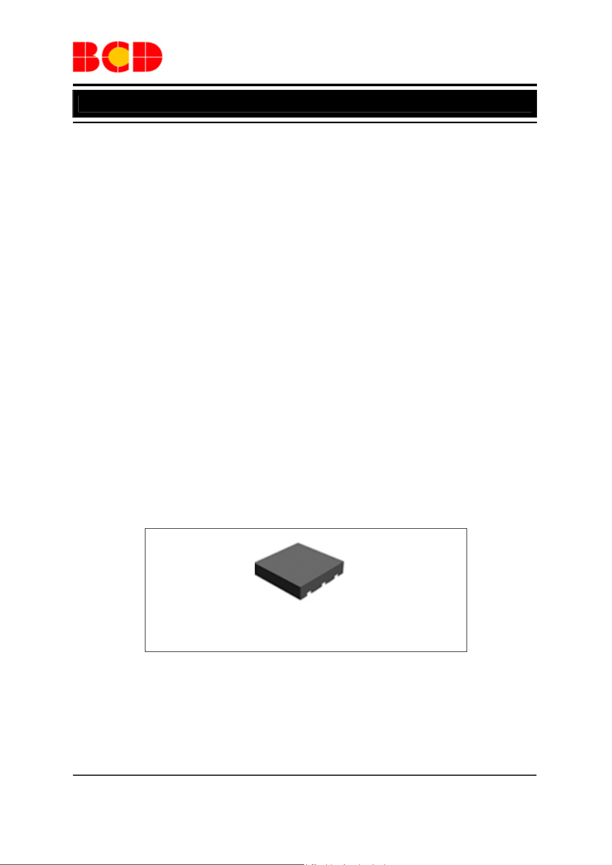
DFN-3×3-6
Figure 1. Package Type of AP 3432
Jun. 2013 Rev. 1. 1 BCD Semiconductor Manufacturing Limited
1
Data Sheet
1.5MHz, 2.5A, Step-down DC-DC Converter AP3432
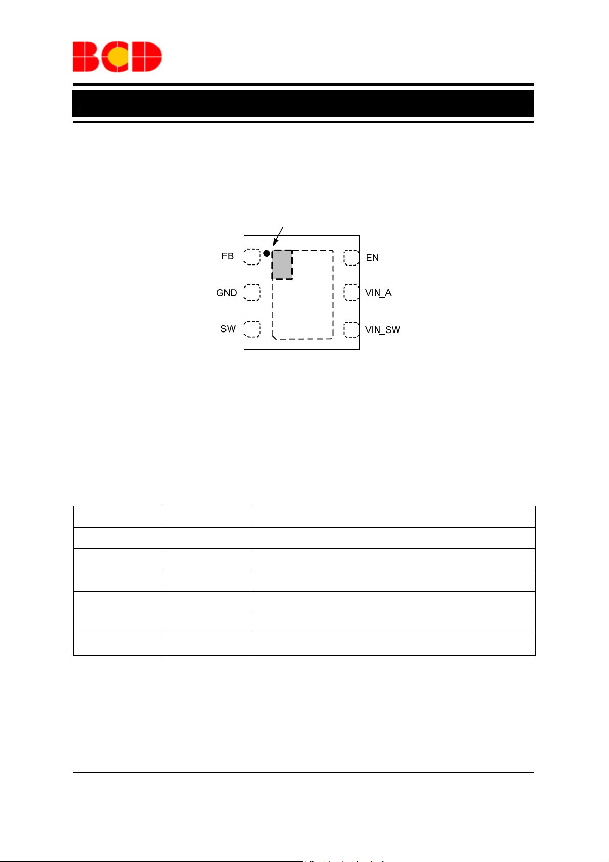
Pin Configuration
DN Package
(DFN-3×3-6)
Pin 1 Mark
1
2
Figure 2. Pin Configuration of AP3432 (Top View)
Exposed
Pad
6
5
43
Pin Description
Pin Number Pin Name Function
1 FB Output voltage feedback pin
2 GND Ground pin
3 SW Switch output pin
4 VIN_SW Power supply input for the MOSFET switch
5 VIN_A Supply input for the analog circuit
6 EN Enable pin, active high
Jun. 2013 Rev. 1. 1 BCD Semiconductor Manufacturing Limited
2
Data Sheet
1.5MHz, 2.5A, Step-down DC-DC Converter AP3432
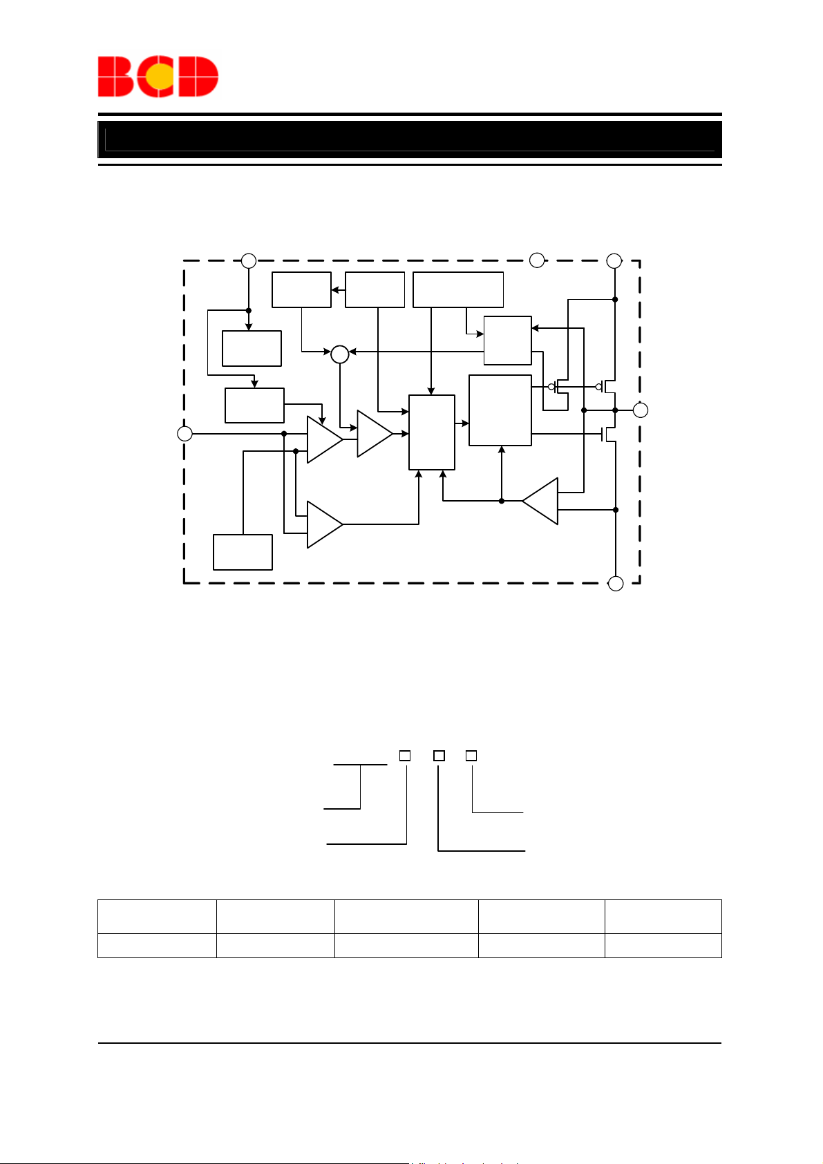
Functional Block Diagram
-
+
VIN_SW
4
3
2
GND
SW
FB
1
EN
6
Bias
Generator
Soft
Start
Bandgap
Reference
VIN_A
Saw-tooth
Generator
Oscillator
+
-
+
Error
Amplifier
+
-
Modulator
-
+
Over Voltage
Comparator
Figure 3. Functional Block Diagram of AP3432
Over Current
Comparator
Control
Logic
Reverse Inductor
Current Comparator
Current
Sensing
Buffer &
Dead Time
Control
Logic
5
Ordering Information
AP3432 -
Circuit Type
Package
DN: DFN-3×3-6
G1: Green
TR: Tape & Reel
Package
DFN-3×3-6 -40 to 80°C AP3432DNTR-G1 BQA Tape & Reel
Temperature
Range
Part Number Marking ID Packing Type
BCD Semiconductor's Pb-free products, as designated with "G1" in the part number, are RoHS compliant and
green.
Jun. 2013 Rev. 1. 1 BCD Semiconductor Manufacturing Limited
3
Data Sheet
1.5MHz, 2.5A, Step-down DC-DC Converter AP3432
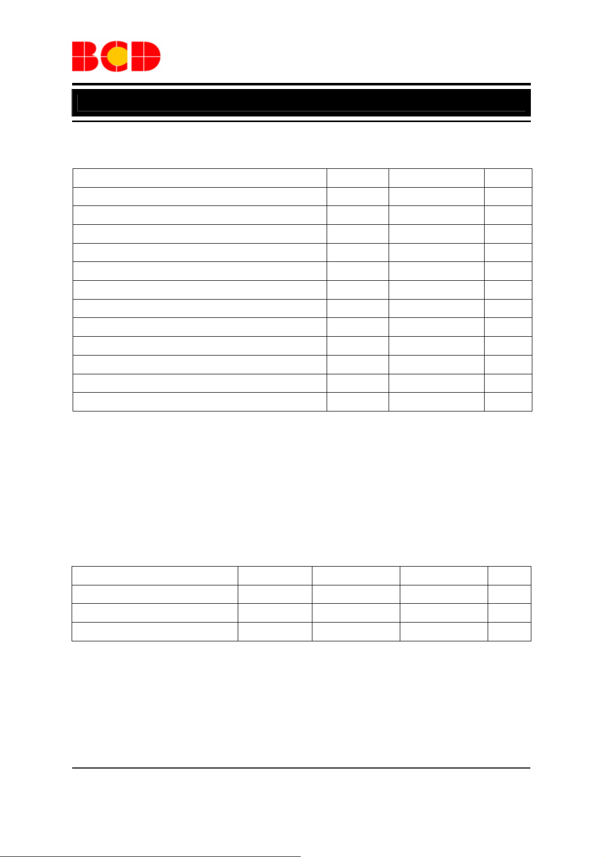
Absolute Maximum Ratings (Note 1)
Parameter Symbol Value Unit
Supply Input Voltage ( pin VIN_SW) V
Supply Input Voltage ( pin VIN_A) V
SW Pin Switch Voltage VSW -0.3 to V
Enable Voltage VEN -0.3 to V
SW Pin Switch Current ISW 3.5 A
Power Dissipation (On PCB, TA=25°C) PD
Thermal Resistance (Junction to Ambient, Simulation) θJA
Operating Junction Temperature TJ
Operating Temperature TOP
Storage Temperature T
ESD (Human Body Model) V
ESD (Machine Model) VMM
Note 1: Stresses greater than those listed under “Absolute Maximum Ratings” may cause permanent damage to
the device. These are stress ratings only, and functional operation of the device at these or any other conditions
beyond those indicated under “Recommended Operating Conditions” is not implied. Exposure to “Absolute
Maximum Ratings” for extended periods may affect device reliability.
IN_SW
IN_A
STG
HBM
0 to 6.5
0 to 6.5
IN_SW
IN_A
2.49
40.11
150
-40 to 85
-55 to 150
2000
200
+0.3 V
+0.3 V
V
V
W
°C/W
°C
°C
°C
V
V
Recommended Operating Conditions
Parameter Symbol Min Max Unit
Supply Input Voltage VIN 2.7 5.5 V
Junction Temperature Range TJ -40 125 °C
Ambient Temperature Range TA -40 80 °C
Jun. 2013 Rev. 1. 1 BCD Semiconductor Manufacturing Limited
4

Data Sheet
1.5MHz, 2.5A, Step-down DC-DC Converter AP3432
Electrical Characteristics
V
IN_SW=VIN_A=VEN
otherwise specified.
Parameter Symbol Conditions Min Typ Max Unit
Input Voltage Range VIN 2.7 5.5 V
=5V, V
=1.2V, VFB=0.8V, L=3.3H, CIN=4.7F, C
OUT
=22F, TA=25°C, unless
OUT
Shutdown Current I
Active Current ION V
Regulated Feedback
Voltage
Regulated Output
Voltage Accuracy
V
Peak Inductor
Current
Oscillator Frequency f
PMOSFET RON R
NMOSFET RON R
EN High-level Input
Voltage
EN Low-level Input
Voltage
V
OFF
For Adjustable Output Voltage 0.784 0.8 0.816 V
V
FB
OUT/VOUT
I
OSC
ON(P)
ON(N)
V
EN_H
V
EN_L
3.0 3.5 A
PK
1.2 1.5 1.8 MHz
ISW=0.75A 100 m
ISW=0.75A 100 m
1.5 V
0.4 V
=0V 1 A
EN
=0.95V 310 A
FB
=2.7V to 5.5V, I
V
IN
to 2.5A
OUT
=10mA
-3 3 %
EN Input Current IEN 1 A
Soft-start time tSS 400 S
Maximum Duty
Cycle
Under Voltage Lock
Out
100 %
D
MAX
Rising 2.4
V
UVLO
Falling 2.3
V
Hysteresis Hysteresis 0.1 V
OVP Threshold V
5.8 5.9 6.0 V
OVP
Hysteresis on OVP 300 400 500 mV
Thermal Shutdown TSD Hysteresis=30°C 150 °C
Jun. 2013 Rev. 1. 1 BCD Semiconductor Manufacturing Limited
5
Data Sheet
1.5MHz, 2.5A, Step-down DC-DC Converter AP3432
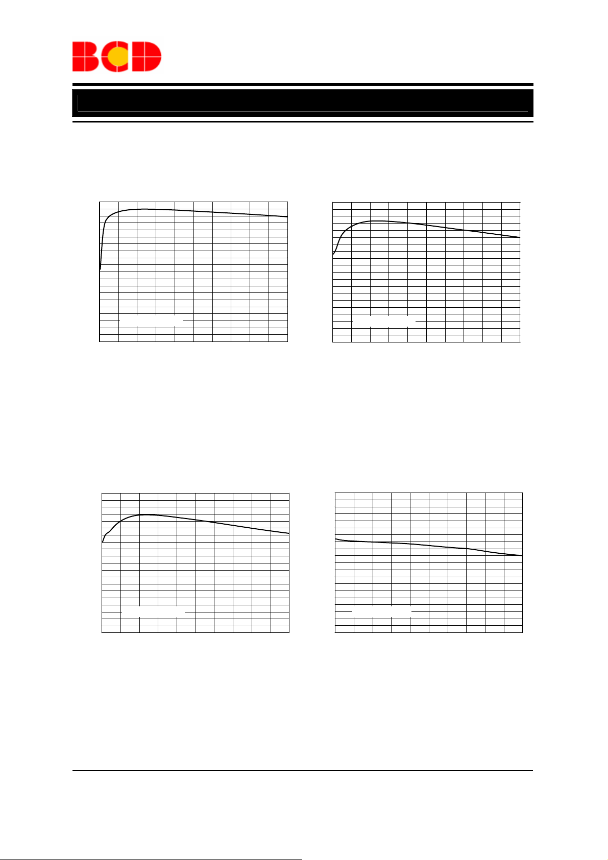
Typical Performance Characteristics
100
90
80
70
60
50
Efficiency (%)
40
30
20
10
0
VIN=5V, V
0.00.51.01.52.02.5
OUT
=3.3V
Output Current (A)
Figure 4. Efficiency vs. Output Current Figure 5. Efficiency vs. Output Current
100
90
80
70
60
50
40
Efficiency (%)
30
20
10
VIN=5V, V
0
0.0 0.5 1.0 1.5 2.0 2.5
OUT
=1.2V
Output Current (A)
100
90
80
70
60
50
40
Efficiency (%)
30
20
10
0
VIN=5V, V
0.0 0.5 1.0 1.5 2.0 2.5
OUT
=1.0V
Output Current (A)
Figure 6. Efficiency vs. Output Current Figure 7. 3.3V Load Regulation
3.40
3.38
3.36
3.34
3.32
3.30
3.28
Output Voltage (V)
3.26
3.24
3.22
3.20
VIN=5V, V
0.0 0.5 1.0 1.5 2.0 2.5
OUT
=3.3V
Output Current (A)
Jun. 2013 Rev. 1. 1 BCD Semiconductor Manufacturing Limited
6
 Loading...