Diodes AP3417A User Manual

1A, 1.4MHz High Efficiency Synchronous DC-DC Buck Converter AP3417A
Data Sheet
General Description
The AP3417A is a 1.4MHz fixed frequency, current
mode, PWM synchronous buck (step-down) DC-DC
converter, capable of driving a 1A load with high
efficiency, excellent line and load regulation. The
device integrates synchronous P-channel and
N-channel power MOSFET switches with low
on-resistance. It is ideal for powering portable
equipment that runs from a single Li-ion battery.
A standard series of inductors are available from
several different manufacturers optimized for use
with the AP3417A. This feature greatly simplifies the
design of switch-mode power supplies.
The AP3417A is available in SOT-23-5 package.
Features
• Input Voltage Range: 2.5V to 5.5V
• Output Voltage: 0.6V to V
• ADJ Output
• Fixed 1.4MHz Frequency
• High Efficiency up to 95%
• Output Current: 1A
• Current Mode Control
• 100% Duty Cycle in Dropout
• Built-in Over Current Protection
• Built-in Short Circuit Protection
• Built-in Thermal Shutdown Protection
• Built-in UVLO Function
• Built-in Soft-start
IN
Applications
• Set-top Box
• Datacom
• Portable Device
• Smart Phone
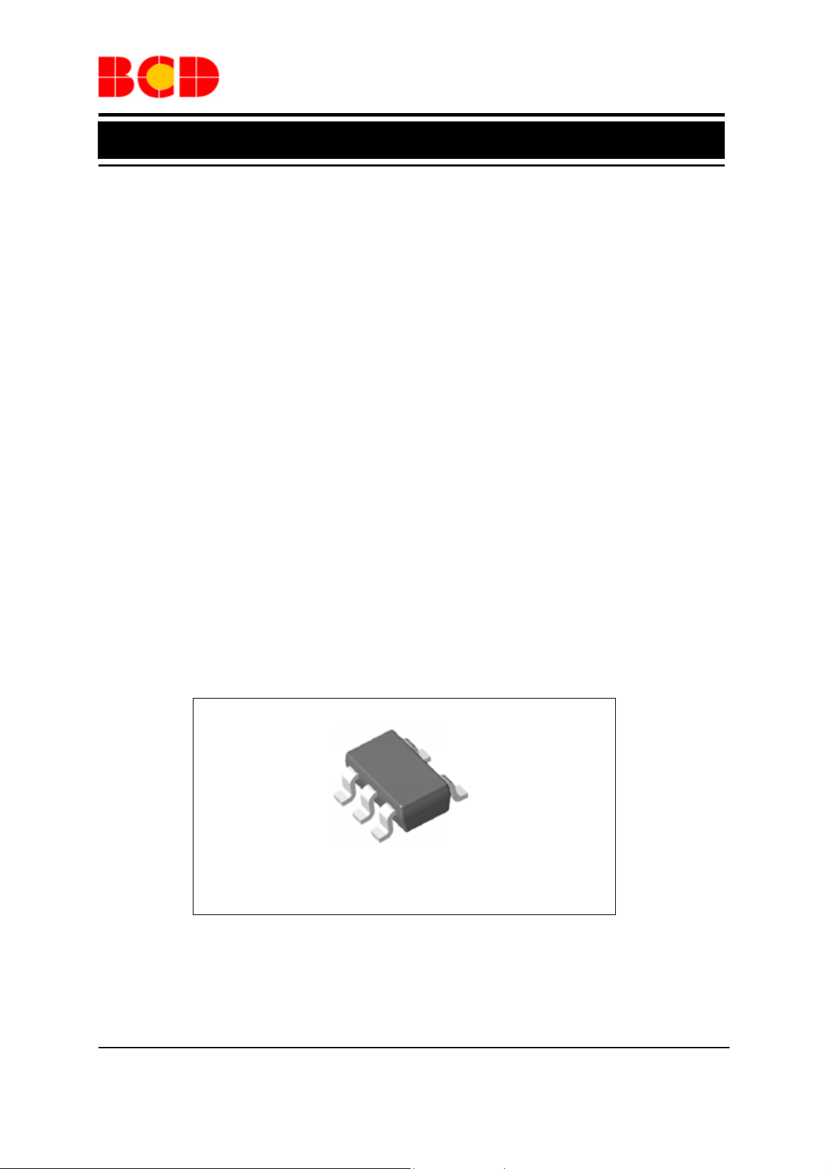
Figure 1. Package Type of AP3417A
SOT-23-5
Aug. 2012 Rev. 1. 2 BCD Semiconductor Manufacturing Limited
1

Data Sheet
1A, 1.4MHz High Efficiency Synchronous DC-DC Buck Converter AP3417A
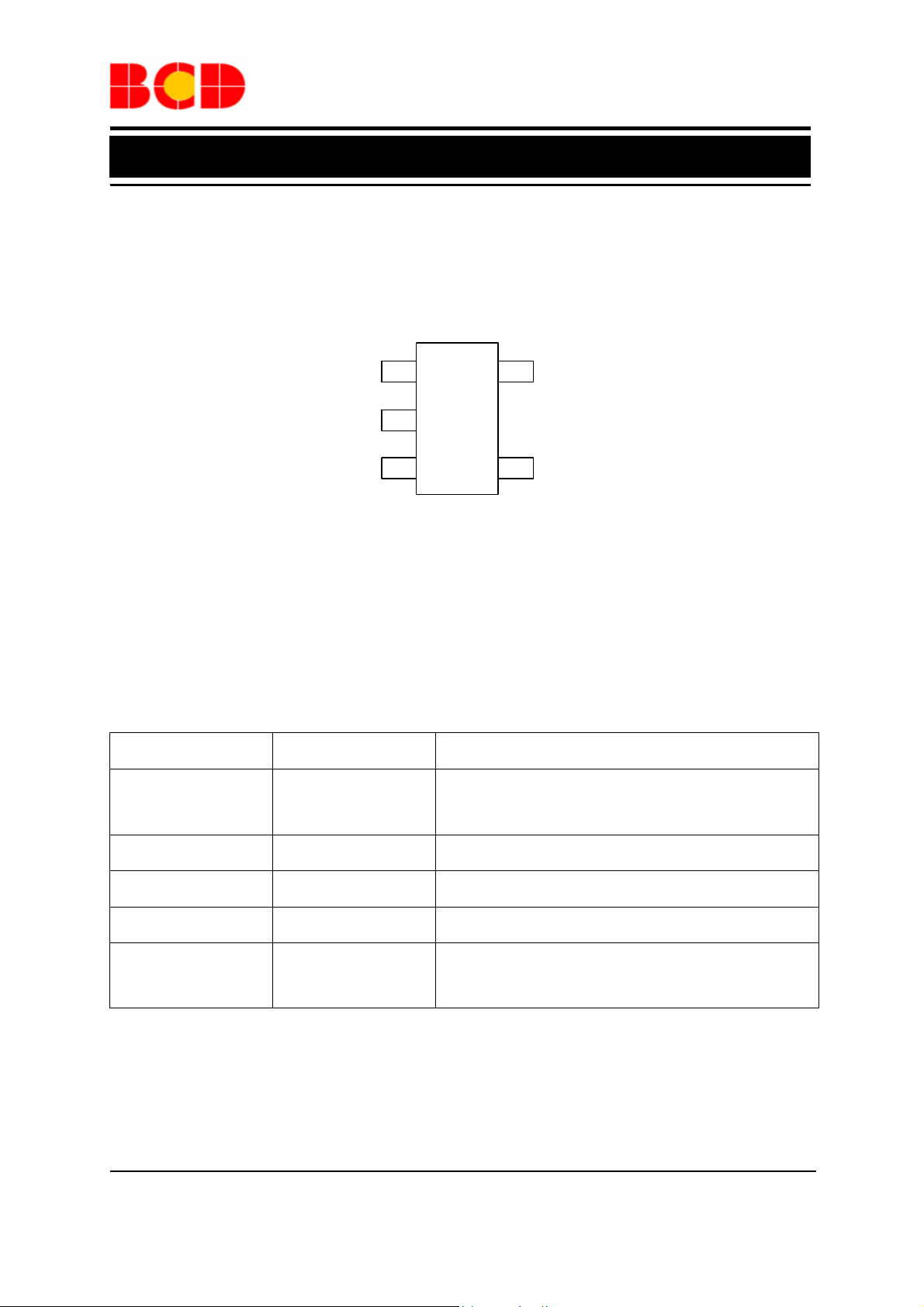
Pin Configuration
K Package
(SOT-23-5)
EN
GND
SW
Figure 2. Pin Configuration of AP3417A (Top View)
1
2
34
5
FB
VIN
Pin Description
Pin Number Pin Name Function
Control input pin. Forcing this pin above 1.5V enables the IC.
1 EN
2 GND Ground pin
3 SW
4 VIN
5 FB
Forcing this pin below 0.4V shuts down the IC. When the IC is
in shutdown mode, all functions are disabled to decrease the
supply current below 1µA
Power switch output pin. Inductor connection to drain of the
internal PFET and NFET switches
Supply input pin. Bypass to GND with a 4.7µF or greater
ceramic capacitor
This is the feedback pin of the device. Connect this pin directly
to the output if the fixed output voltage version is used. For the
adjustable version, an external resistor divider is connected to
this pin
Aug. 2012 Rev. 1. 2 BCD Semiconductor Manufacturing Limited
2

Data Sheet
1A, 1.4MHz High Efficiency Synchronous DC-DC Buck Converter AP3417A
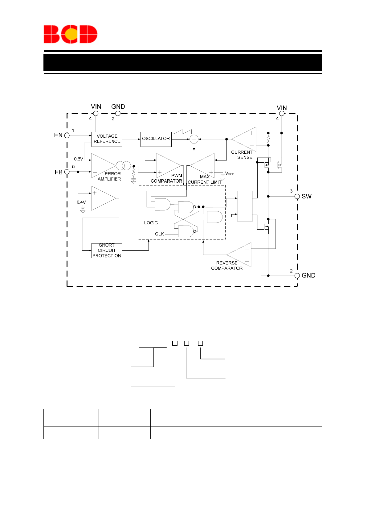
Functional Block Diagram
DRIVER
Figure 3. Functional Block Diagram of AP3417A
Ordering Information
AP3417A -
G1: Green
Circuit Type
K: SOT-23-5
Package
SOT-23-5 -40 to 85 ºC AP3417AKTR-G1 G4H Tape & Reel
BCD Semiconductor's Pb-free products, as designated with "G1" suffix in the part number, are RoHS compliant
and green.
Temperature
Range
Part Number Marking ID Packing Type
TR: Tape & Reel
Aug. 2012 Rev. 1. 2 BCD Semiconductor Manufacturing Limited
3

Data Sheet
1A, 1.4MHz High Efficiency Synchronous DC-DC Buck Converter AP3417A
Absolute Maximum Ratings (Note 1)
Parameter Symbol Value Unit
Input Voltage VIN -0.3 to 6.0 V
Feedback Voltage VFB -0.3 to VIN +0.3 V
EN Pin Voltage VEN -0.3 to VIN+0.3 V
SW Pin Voltage VSW -0.3 to VIN+0.3 V
Thermal Resistance
Operating Junction Temperature TJ 150 ºC
Storage Temperature T
Lead Temperature (Soldering, 10sec) T
ESD(Machine Model) 200 V
ESD(Human Body Model) 2000 V
Note 1: Stresses greater than those listed under “Absolute Maximum Ratings” may cause permanent damage to
the device. These are stress ratings only, and functional operation of the device at these or any other conditions
beyond those indicated under “Recommended Operating Conditions” is not implied. Exposure to “Absolute
Maximum Ratings” for extended periods may affect device reliability.
θ
JA
-65 to 150 ºC
STG
260 ºC
LEAD
265 ºC/W
Recommended Operating Conditions
Parameter Symbol Min Max Unit
Input Voltage VIN 2.5 5.5 V
Operating Ambient Temperature TA -40 85 ºC
Aug. 2012 Rev. 1. 2 BCD Semiconductor Manufacturing Limited
4
 Loading...