

Page 1
SERVICE MANUAL
Copyright 2013 D&M Holdings Inc. All rights reserved.
WARNING: Violators will be prosecuted to the maximum extent possible.
Ver.1
S0768-1V01DM/DG1312
•
Some illustrations using in this service manual are slightly different from the actual set.
•
Please use this service manual with referring to the operating instructions without fail.
• For purposes of improvement, specications and design are subject to change without notice.
D&M Holdings Inc.
MODEL JP E3 E2 EK EA E1 E1K E1C
MC6000MK2EM
P P
Professional Digital Mixer and Controller
Page 2

CONTENTS
ABOUT THIS MANUAL .............................................................3
What you can do with this manual ............................................3
Using Adobe Reader (Windows version) ..................................4
SAFETY PRECAUTIONS ..........................................................6
NOTE FOR SCHEMATIC DIAGRAM .........................................7
NOTE FOR PARTS LIST ...........................................................7
INSTRUCTIONS FOR HANDLING SEMI-CONDUCTORS
AND OPTICAL UNIT .................................................................7
TECHNICAL SPECIFICATIONS ................................................9
DIMENSION .............................................................................10
PRECAUTIONS DURING SERVICE .......................................11
Initializing This Unit .................................................................11
DISASSEMBLY ........................................................................12
SPECIAL MODE ......................................................................23
Special mode setting button ....................................................23
PROCEDURE AFTER REPLACING THE
MICROPROCESSOR, ETC ....................................................34
FIRMWARE UPDATE PROCEDURE ......................................34
TROUBLE SHOOTING ............................................................43
WAVEFORMS and TROUBLESHOOTING .............................51
BLOCK DIAGRAM ...................................................................55
POWER BLOCK DIAGRAM ....................................................56
LEVEL DIAGRAM ....................................................................57
WIRING DIAGRAM ..................................................................58
PRINTED WIRING BOARDS ...................................................59
SCHEMATIC DIAGRAMS (1/5) ...............................................63
MAIN UNIT ..............................................................................63
I/O ..........................................................................................64
CONTROL 1 ............................................................................65
CONTROL 2 ............................................................................66
FRONT ....................................................................................67
EXPLODED VIEW ....................................................................68
PACKING VIEW .......................................................................69
SEMICONDUCTORS ...............................................................70
1. IC's .....................................................................................70
Page 3
ABOUT THIS MANUAL
Read the following information before using the service manual.
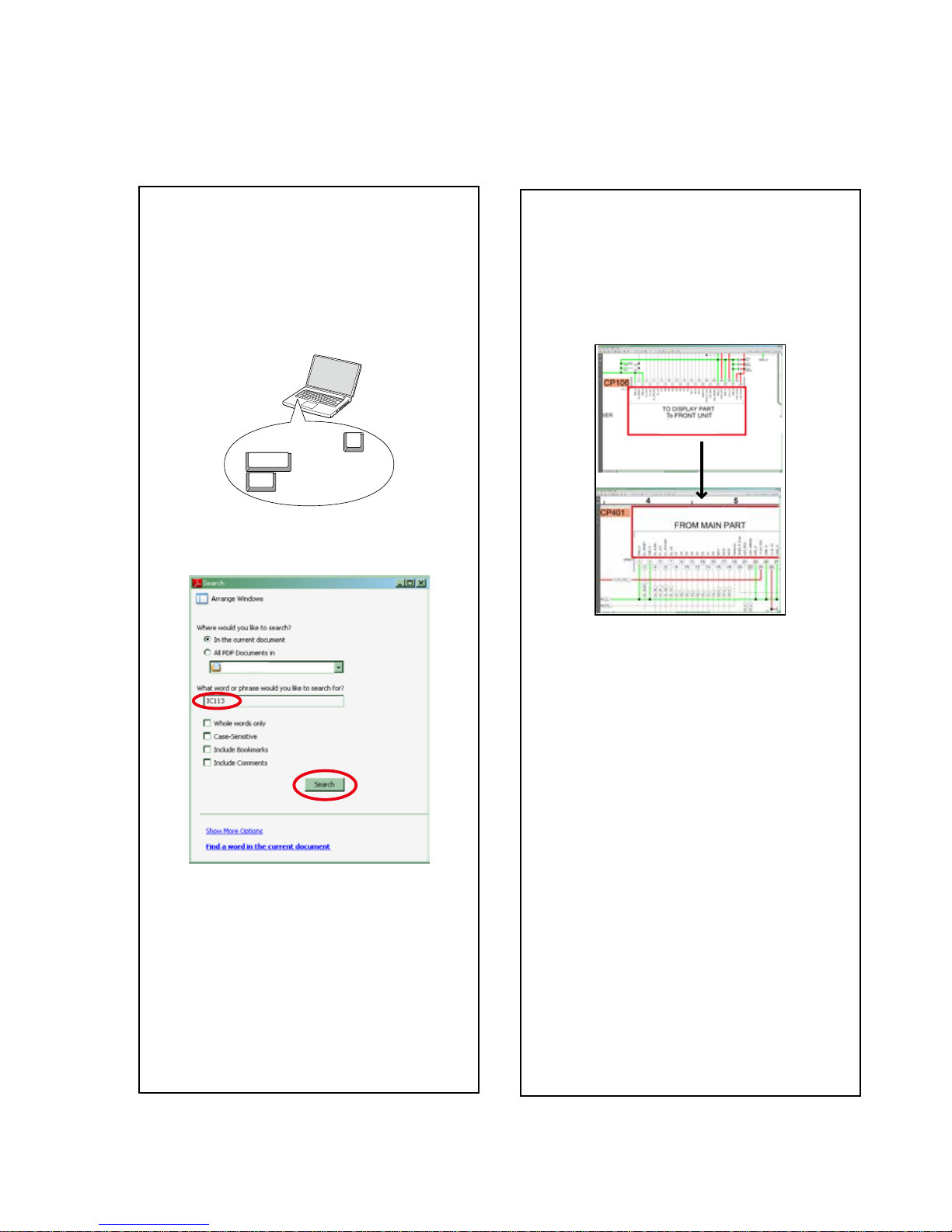
What you can do with this manual
Search for a Ref. No. (phrase)
(Ctrl+Shift+F)
You can use the search function in Acrobat Reader to
search for a Ref. No. in parts lists.
1.Press Ctrl+Shift+F on the keyboard.
• The Search window appears.
2.Enter the Ref. No. you want to search for in the
Search window, and then click the Search button.
•A list of search results appears.
3.Click an item on the list.
• The screen jumps to the page for that item, and the
search phrase is displayed.
Ctrl
Shift
F
Jump to the target of a schematic
diagram connector
Click the Ref. No. of the target connector in the red
box around a schematic diagram connector.
•The screen jumps to the target connector.
•Pagemagnicationstaysthesameasbeforethe
jump.
CP401
CP106
v
3
Page 4

Using Adobe Reader (Windows version)
• Properties
Click this button and check that the printer is set to a
suitable paper size.
• Page to print
Select the following checkbox.
"More Options" : "Current View"
• Page Sizing & Handling
Select the following checkbox.
"Size" / "Size Options" : "Fit"
Add notes to this data (Sign)
The Sign function lets you add notes to the data in
this manual.
Savetheleonceyouhavenishedaddingnotes.
[Example using Adobe Reader X]
On the "View" menu, click "Sign".
• The Sign pane appears.
[Example using Adobe Reader 9]
On the "Document" menu, click "Sign".
Magnify schematic / printed wiring
board diagrams - 1
(Ctrl+Space, mouse operation)
Press Ctrl+Space on the keyboard and drag the
mouse to select the area you want to view.
• Theselectedareaismagnied.
• When you want to move the area shown, hold
down Space and drag the mouse.
• When you want to show a full page view, press
Ctrl+0 on the keyboard.
Ctrl Space
0
Print a magnied part of the manual
The Properties dialog box and functions will vary depending on your printer.
1. Drag the mouse to magnify the part you want to print.
2. On the "File" menu, click "Print".
3. CongurethefollowingsettingsinthePrintdialogbox.
4. Click the Print button to start printing.
4
Page 5
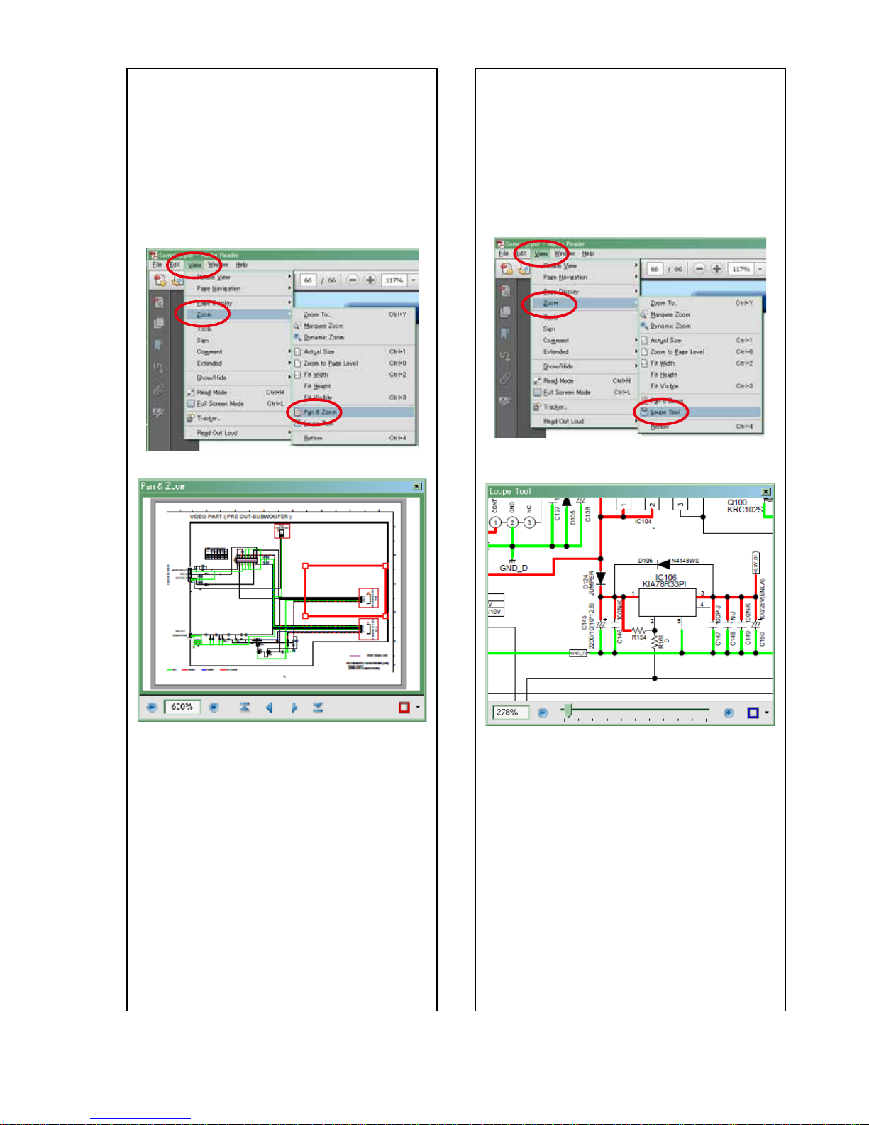
Magnify schematic / printed wiring
board diagrams - 2
(Pan & Zoom function)
The Pan & Zoom function lets you see which part of
amagnieddiagramisbeingshowninaseparate
window.
[Example using Adobe Reader X]
On the "View" menu, point to "Zoom", and then click
"Pan & Zoom".
• The Pan & Zoom window appears on the screen.
[Example using Adobe Reader 9]
On the "Tools" menu, point to "Select & Zoom", and
then click "Pan & Zoom Window".
Magnify schematic / printed wiring
board diagrams - 3
(Loupe Tool function)
TheLoupeToolfunctionletsyoumagnifyaspecic
part of a diagram in a separate window.
[Example using Adobe Reader X]
On the "View" menu, point to "Zoom", and then click
"Loupe Tool".
• The Loupe Tool window appears on the screen.
[Example using Adobe Reader 9]
On the "Tools" menu, point to "Select & Zoom", and
then click "Loupe Tool Window".
5
Page 6

SAFETY PRECAUTIONS
The following items should be checked for continued protection of the customer and the service technician.
leakage current check
Before returning the set to the customer, be sure to carry out either (1) a leakage current check or (2) a line to chassis
resistance check. If the leakage current exceeds 0.5 milliamps, or if the resistance from chassis to either side of the
power cord is less than 460 kohms, the set is defective.
Be sure to test for leakage current with the AC plug in both polarities, in addition, when the set's power is in each state
(on, off and standby mode), if applicable.
CAUTION
Please heed the following cautions and instructions during servicing and
inspection.
◎Heed the cautions!
Cautions which are delicate in particular for servicing
are labeled on the cabinets, the parts and the chassis,
etc. Be sure to heed these cautions and the cautions
described in the handling instructions.
◎Cautions concerning electric shock!
(1) An AC voltage is impressed on this set, so if you
touch internal metal parts when the set is energized,
you may get an electric shock. Avoid getting an
electric shock, by using an isolating transformer
and wearing gloves when servicing while the set is
energized, or by unplugging the power cord when
replacing parts, for example.
(2) There are high voltage parts inside. Handle with
extra care when the set is energized.
◎ Caution concerning disassembly and
assembly!
Through great care is taken when parts were
manufactured from sheet metal, there may be burrs on
theedgesofparts.Theburrscouldcauseinjuryifngers
are moved across them in some rare cases. Wear gloves
to protect your hands.
◎Use only designated parts!
Theset'spartshavespecicsafetyproperties(re
resistance, voltage resistance, etc.). Be sure to use parts
which have the same properties for replacement. The
burrs have the same properties. In particular, for the
important safety parts that are indicated by the z mark
on schematic diagrams and parts lists, be sure to use
the designated parts.
◎ Be sure to mount parts and arrange the wires
as they were originally placed!
For safety seasons, some parts use tapes, tubes or other
insulating materials, and some parts are mounted away
from the surface of printed circuit boards. Care is also
taken with the positions of the wires by arranging them
and using clamps to keep them away from heating and
high voltage parts, so be sure to set everything back as
it was originally placed.
◎Make a safety check after servicing!
Check that all screws, parts and wires removed or
disconnected when servicing have been put back in their
original positions, check that no serviced parts have
deteriorate the area around. Then make an insulation
check on the external metal connectors and between
the blades of the power plug, and otherwise check that
safety is ensured.
(Insulation check procedure)
Unplug the power cord from the power outlet, disconnect
the antenna, plugs, etc., and on the power. Using a 500V
insulation resistance tester, check that the insulation
resistance value between the inplug and the externally
exposed metal parts (antenna terminal, headphones
terminal,inputterminal,etc.)is1MΩorgreater.Ifitis
less, the set must be inspected and repaired.
Many of the electric and the structural parts used in the
set have special safety properties. In most cases these
propertiesaredifculttodistinguishbysight,andtheuse
of replacement parts with higher ratings (rated power
and withstand voltage) does not necessarily guarantee
that safety performance will be preserved. Parts with
safety properties are indicated as shown below on the
wiring diagrams and the parts list in this service manual.
Be sure to replace them with the parts which have the
designated part number.
(1) Schematic diagrams .......Indicated by the z mark.
(2) Parts lists .......Indicated by the z mark.
The use of parts other than the
designated parts could cause electric
shocks,resorotherdangerous
situations.
CAUTION
Concerning important
safety parts
6
Page 7

NOTE FOR SCHEMATIC DIAGRAM
WARNING:
Parts indicated by the z mark have critical characteristics. Use ONLY replacement parts recommended by the manufacturer.
CAUTION:
Before returning the set to the customer, be sure to carry out either (1) a leakage current check or (2) a line to chassis resistance check.
If the leakage current exceeds 0.5 milliamps, or if the resistance from chassis to either side of the power cord is less than 460 kohms, the
set is defective.
WARNING:
DONOTreturnthesettothecustomerunlesstheproblemisidentiedandremedied.
NOTICE:
ALL RESISTANCE VALUES IN OHM. k=1,000 OHM / M=1,000,000 OHM
ALL CAPACITANCE VALUES ARE EXPRESSED IN MICRO FARAD, UNLESS OTHERWISE INDICATED. P INDICATES MICRO-MICRO
FARAD. EACH VOLTAGE AND CURRENT ARE MEASURED AT NO SIGNAL INPUT CONDITION. CIRCUIT AND PARTS ARE SUBJECT
TO CHANGE WITHOUT PRIOR NOTICE.
INSTRUCTIONS FOR HANDLING SEMI-CONDUCTORS AND OPTICAL UNIT
Electrostatic breakdown of the semi-conductors or optical pickup may occur due to a potential difference caused by
electrostatic charge during unpacking or repair work.
1. Ground for Human Body
Besuretowearagroundingband(1MΩ)thatisproperlygroundedtoremoveanystaticelectricitythatmaybecharged
on the body.
2. Ground for Workbench
Besuretoplaceaconductivesheetorcopperplatewithpropergrounding(1MΩ)ontheworkbenchorothersurface,
where the semi-conductors are to be placed. Because the static electricity charge on clothing will not escape through the
body grounding band, be careful to avoid contacting semi-conductors with your clothing
<Incorrect>
CBA
Grounding Band
Conductive Sheet or
Copper Plate
1MΩ
1MΩ
<Correct>
CBA
NOTE FOR PARTS LIST
1. Parts indicated by "nsp" on this table cannot be supplied.
2. When ordering a part, make a clear distinction between "1" and "I" (i) to avoid mis-supplying.
3. A part ordered without specifying its part number can not be supplied.
4. Part indicated by "★" mark is not illustrated in the exploded view.
WARNING: Parts indicated by the z mark have critical characteristics. Use ONLY replacement parts recommended by the
manufacturer.
7
Page 8

Personal notes:
8
Page 9

9
TECHNICAL SPECIFICATIONS
n
Audio
(0 dBu=0.775 Vrms, 0 dBV =1 Vrms)
・
PHONO inputs
2 Stereo
Unbalanced RCA terminal
Input impedance:
50 kΩ/kohms
Level:
–40 dBV(10 mV)
Signal to Noise ratio:
Over 82 dB
・
LINE 1, 2 inputs
2 Stereo
Unbalanced RCA terminal
Input impedance:
10 kΩ/kohms
Level:
0 dBV
Signal to Noise ratio:
Over 84 dB
・
LINE 3, 4 inputs
2 Stereo
Unbalanced RCA terminal
Input impedance:
10 kΩ/kohms
Level:
0 dBV
Signal to Noise ratio:
82 dB or later
・
Equalizer (CH)
3 Band
Channel EQ Adjustment Range:
HI (High Range) : –∞, –90 dB – +10 dB
MID (Medium Range) : –∞, –90 dB – +10 dB
LOW (Low Range) : –∞, –90 dB – +6 dB
・
MIC inputs
2 Monaural
MIC 1:
Combo jack
(terminal for balanced XLR and balanced 1/4 inch TRS)
(1: ground, 2: hot, 3: cold, chip: hot, ring: cold, sleeve: ground)
MIC 2:
Balanced 1/4 inch TRS terminal
Input impedance:
5 kΩ/kohms
Level:
–60 dBu – –16 dBu
・
Equalizer (MIC)
3 Band
Adjustment Range:
HI (High Range) : –15 – +15 dB
MID (Medium Range) : –15 – +15 dB
LOW (Low Range) : –15 – +15dB
・
USB audio inputs
2 Stereo (4 Monaural) 16 bit, Fs : 44.1 kHz USB B
・
MASTER output
Balanced:
Stereo, balanced XLR terminal
(1: Ground, 2: Hot, 3: Cold)
DA converter:
24 bit
Load impedance:
Over 600 Ω/ohms
Level:
+ 4 dBu (Max + 24 dBu)
When RL=100 kΩ/kohms
Frequency response:
20 Hz – 20 kHz (±1 dB)
THD:
Less than 0.05%
Crosstalk:
Less than –90 dB (1 kHz)
Unbalanced:
Stereo RCA terminal
Load impedance:
100 kΩ/kohms
Level:
0 dBu (Max + 20dBu)
・
BOOTH Output
Stereo balanced 1/4 inch TRS terminal
Load impedance:
Over 600 Ω/ohms
Level:
+ 4 dBu (Max + 24 dBu)
When RL=100 kΩ/kohms
・
Headphone output
Stereo
Load impedance:
40 Ω/ohms
Level:
100 mW
・
USB audio output
2 Stereo (4 Monaural) 16 bit, 44.1 kHz USB B
n
General
USB MIDI I/O:
IN: 1ch, OUT: 1ch MIDI 1.0, MIDI Clock USB B
CH/MASTER Meter:
PPM 7 Point LED –20 – +10 dB, Peak
CH Fader:
45 mm Slim Type Fader
Cross Fader:
45 mm Fader
・
Power voltage:
DC12V (the unit)
AC adapter input:
U.S.A. and Canada models:
AC 120 V, 60 Hz
European,U.K. and Asia/
Pacific models:
AC 230 V, 50 Hz
AC adapter output:
DC 12V 3A
Power consumption:
24 W
Operating temperature:
+5 °C – +35 °C
Operating humidity:
25 % – 85 %
Storage temperature:
–20 °C – 60 °C
For the purpose of improvement, the specications and design are subject to change without notice.
Page 10
10
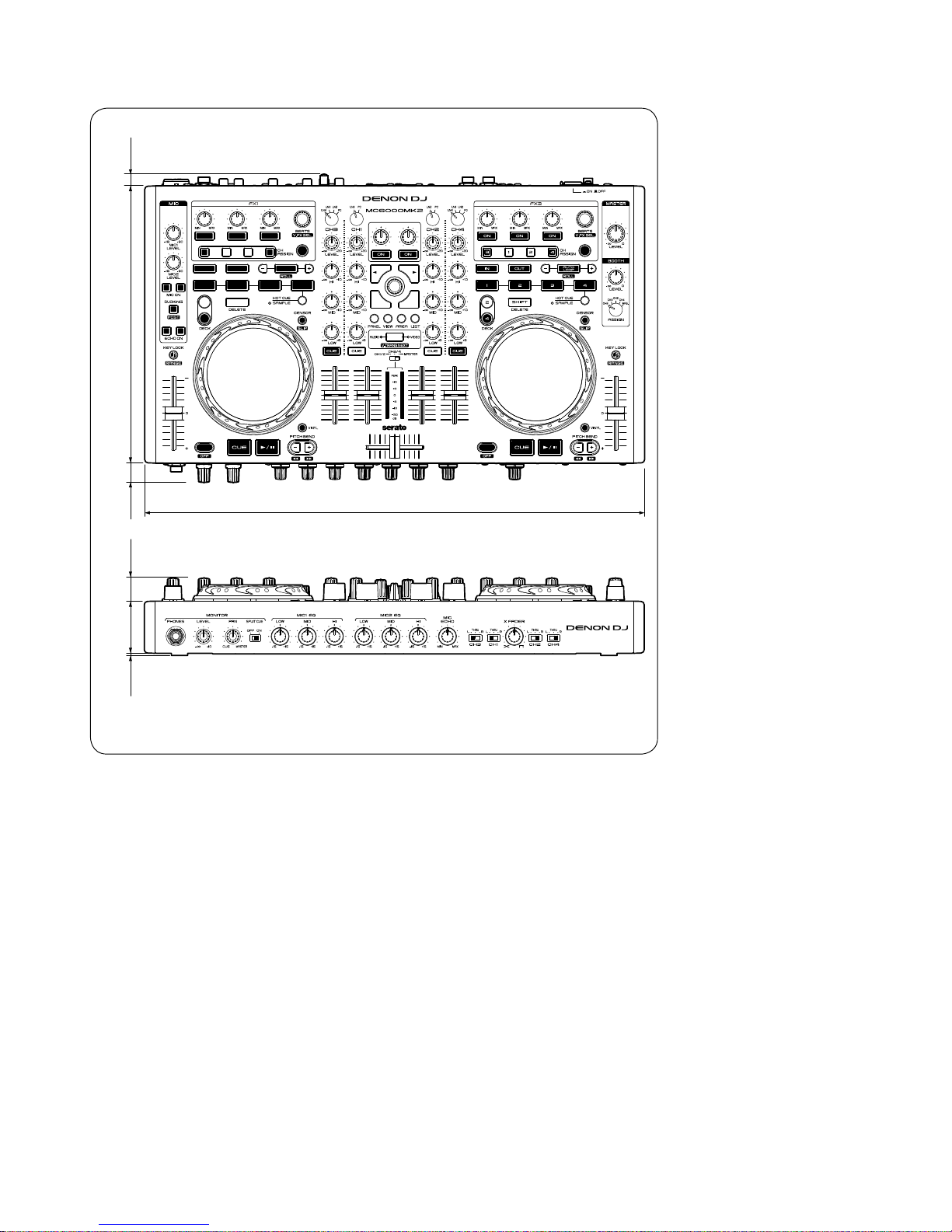
DIMENSION
Unit : in. (mm)
18 11/32
(460.0)
7/16
(11.0)
27/32
(21.5)
1 57/64
(48.0)
10 3/64
(255.0)
45/64
(17.7)
5/64
(2.0)
Weight : 9 lbs 8 oz (4.3 kg)
Page 11

11
Initializing This Unit
Initialize this unit if you have replaced the microprocessor, one of the parts around the microprocessor, or the main PWB.
1. Turn on the power while pressing the BACK, FWD and X-F LINK buttons simultaneously.
2. Return to default setting, and these data (as follows) turn to factory default setting.
Upon completion of the adjustment, it automatically restarts, start in Normal mode.
NOTE: • The parameters will be lost and the factory setting will be recovered after the set is initialized.
So make sure to note down your setting beforehand for restoring after the initialization.
PRECAUTIONS DURING SERVICE
Power operation switch
BACK FWD
X-F LINK
Page 12
12
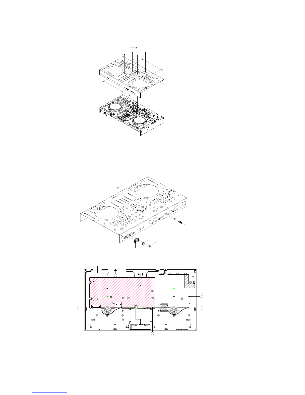
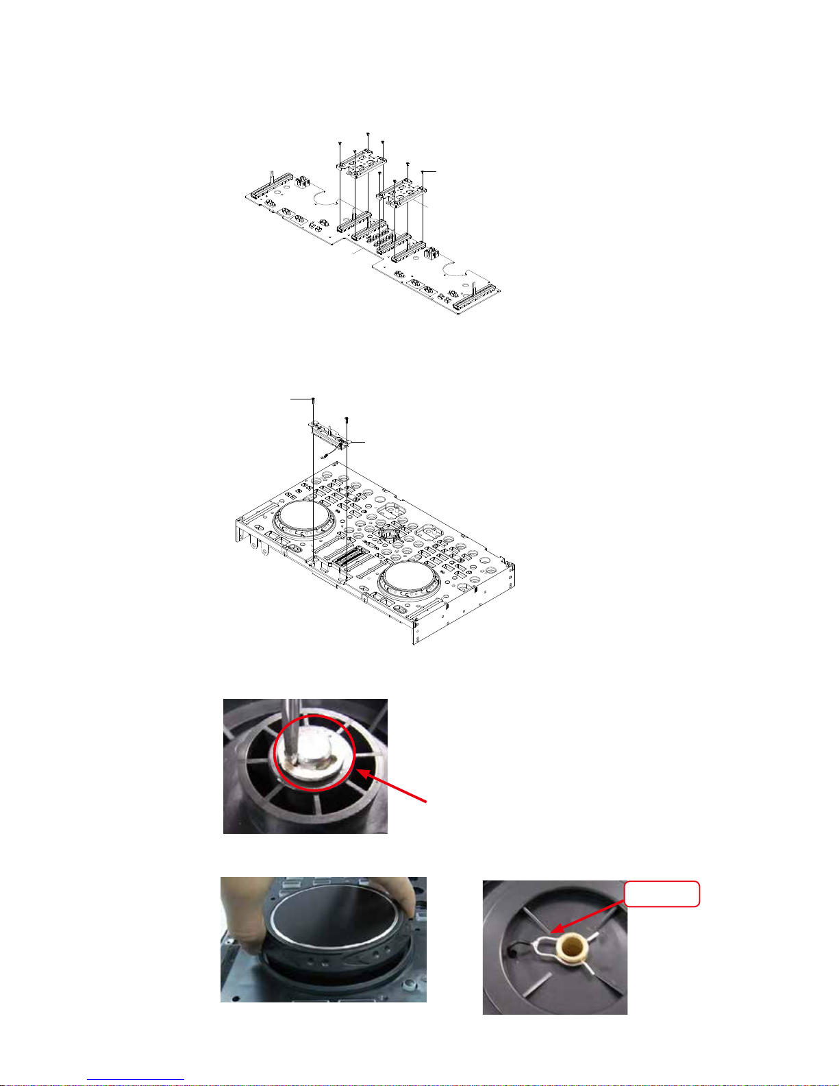
DISASSEMBLY
• Remove each part in the order of the arrows below.
• Reassemble removed parts in the reverse order.
• Read“ SAFETY PRECAUTION” before reassembling removed parts.
• If wire bundles are removed or moved during adjustment or part replacement, reshape the wires after completing the
work. Failure to shape the wires correctly may cause problems such as noise.
SIDE COVER, BASE(BOTTOM PANNEL)
Refer to "DISASSEMBLY 1.- 4.3."
and "EXPLODED VIEW"
(Ref. No. of EXPLODED VIEW : 25, 31)
FRONT PANEL
Refer to "DISASSEMBLY 12."
and "EXPLODED VIEW"
(Ref. No. of EXPLODED VIEW : 4-2)
Caution
Tighten removed screws in the following steps.
1. Front(TOP) panel screws.(See DISASSEMBLY 11.)
2. Rear panel screws.(See DISASSEMBLY 4-2.)
3. Front panel screws.(See DISASSEMBLY 4-3.)
4. Bottom screws.(See DISASSEMBLY 4-1.)
5. Side cover screws.(See DISASSEMBLY 2.)
IO, MAIN and FRONT PWB
Refer to "DISASSEMBLY 5-1.-11."
and "EXPLODED VIEW"
IO PWB: (Ref. No. of :EXPLODED VIEW : 8)
MAIN PWB: (Ref. No. of :EXPLODED VIEW : 7)
FRONTIO PWB: (Ref. No. of :EXPLODED VIEW : 9)
CROSS FADER ASSY
Refer to "DISASSEMBLY 21"
and "EXPLODED VIEW"
(Ref. No. of EXPLODED VIEW : 10)
CONTROL1, CONTROL 2 PWB
Refer to "DISASSEMBLY 13-20"
and "EXPLODED VIEW"
(Ref. No. of EXPLODED VIEW : 5, 6)
WHEEL ASSY
Refer to "DISASSEMBLY 22"
and "EXPLODED VIEW"
(Ref. No. of EXPLODED VIEW : 3)
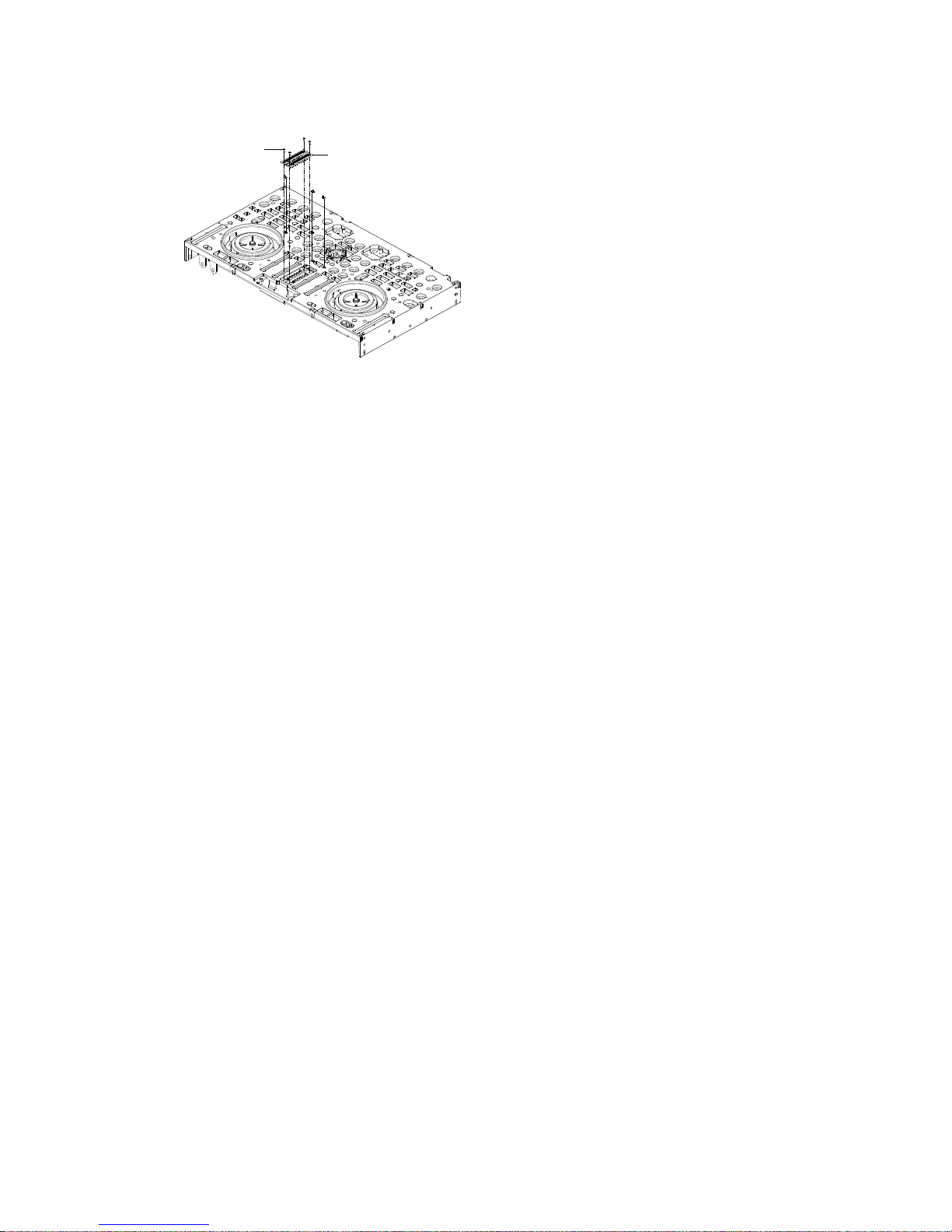
Page 13
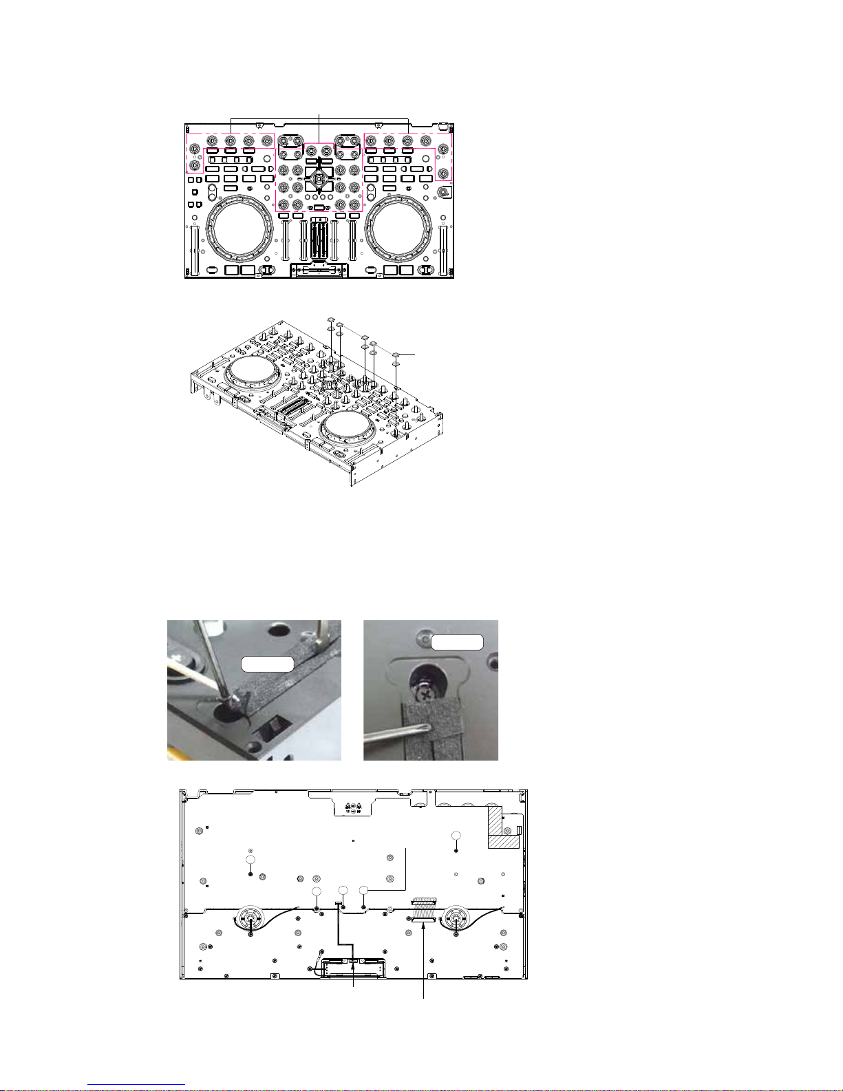
13
Explanatory Photos for“ DISASSEMBLY”
• The angles from which the photos are taken are shown by“ Photo angle: A, B, C, D“ .
• See the diagram below about the shooting direction of each photograph.
• Photographs with no shooting direction indicated were taken from the top of the set.
1. Dismantle the packaging, taking out the machine.
2. Remove the screws*12 from side cover.
Reassemble the rear panel by the 5th step. Step of screw tightening.(1-6)
Side Cover*2
5
6
1
5
4
3
6
2
Screw*6
1
2
3
4
Screw*6
Shooting direction: B
(Rear side)
Shooting direction: D
(Top side)
Shooting direction: A
(Front side)
Shooting direction: C
(Bottom side)
Page 14

14
3. Remove the rotary knob *41 and push knob*6 from panel.
4-1. Remove the screws*12 from bottom base.
Reassemble the bottom base by the 4th step. Step of screw tightening from1 to 12.
Caution on assembly of the bottom panel.
To push one hande and hold at.
4-2. Remove the screws*6 from rear panel.
Reassemble the rear panel by the 2nd step. Step of screw tightening (1-6).
4-3. Remove the screws*6 from front panel.
Reassemble the front panel by the 3rd step. Step of screw tightening from (1-6).
1
screw*6
2
3
4
5
6
1
3
2
4
5
6
screw*6
screw*12
1
2
3
4
5
6
7
8
9
10
11
12
Page 15
15
5-1. Disconnect the FCC cable(follow Figure A).
5-2. Remove the MAIN pcb ass'y.(follow Figure A).
Shooting direction: C (Bottom side)
6. Remove the nuts*12 and washer *12.
7. Remove the screws*15 and remove power button.
Step of screw tightening.(1-10)
8. Disconnect the FCC cable and connector wire and remove cable tie.(follow Figure B).
screw*1
MAIN pcb ass'y
Power button
screw*1
3
2
1
screw*3
screw*10
1
2
3
4
5
6
7
8
9
10
MAIN PWB ASSY
↓
Figure A
Figure B
Page 16
16
9. Disconnect the FCC cable and connector wire.(follow Figure C).
Shooting direction: C (Bottom side)
10. Remove the screw*4
Step of screw tightening.(1-4)
11. Remove the screws *14 from front panel.
Reassemble the front panel by the rst step. Step of screw tightening (1-14).
Caution on assembly of the button.
Adjust and assemble the top panel in the center of the hole.
Press a place other than the center of the button, to conrm that do not catch button on the panel. FAIL
4
3
2
1
Screw*2
FRONT pcb ass'y
Screw*2
1
8
2
3
4
5
6
7
14
13
12
11
10
9
screw*14
Figure C
Page 17
17
12. Remove the screws *10 from front panel.
Step of screw tightening.(1-10)
13-1. Remove screw .buckle and knob protector.
13-2. Remove gound pin . Washer and nut.
13-3. Remove screw*8. (①-⑤)
1
2
3
4
6
5
9
10
7
8
screw*2
screw*2
screw*6
Screw*1
Ground pin
Washer
Nut
Buckle*1
Knob protector
CONTROL 1 PCB
5
63
4
8
7
CN100
CN100
CONTROL 2 PCB
1
screw*8
2
1
2
3
4
6
5
9
10
7
8
screw*2
screw*2
screw*6
Page 18
18
14. Remove nuts*36 and washers*36.
15-1. Remove screw*4. (SCREW*2x2)
15-2. Remove screw*5.(①-⑤)
15-3. Disconnect 32P FFC cable.
15-4. Remove the control 1 pcb ass'y.
nut and washer
(10Φ,31P.S.)
nut and washer
(11Φ,5P.S.)
nut and washer
(10Φ,31P.S.)
nut and washer
(11Φ,5P.S.)
5
3P wire
CN100
CN100
32P FFC cable
CONTROL 1 PCB ASS'Y
3
1
screw*5
4
2
CONTROL 2 PCB ASS'Y
screw*2
screw*2
Page 19
19
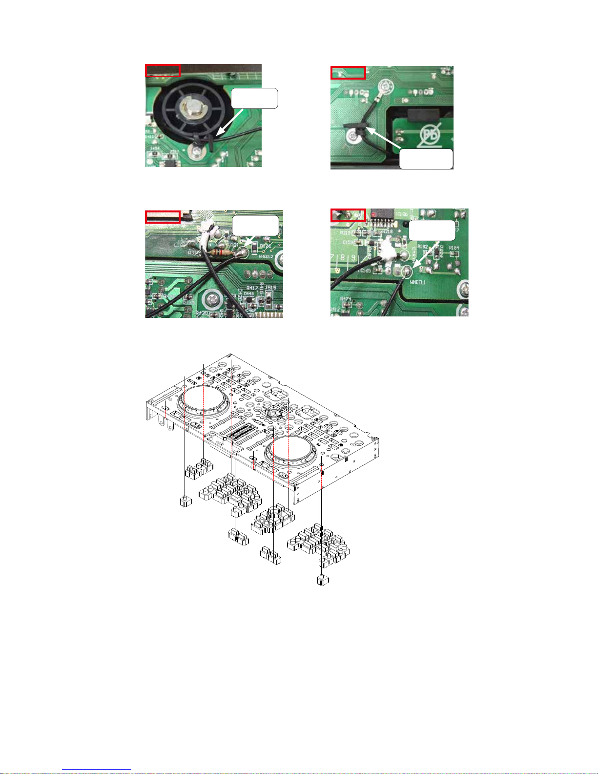
16-1. Release the clamp*2(follow Figure D&E).
16-2. Remove the solder *2.(follow Figure F&G) then remove the control 2 pcb ass'y.
17. Remove the square buttons and rotary buttons.
Release
the clamp
Figure D
Figure E
Figure F
Figure E
Release the
clamp
Remove
the solder
Remove
the solder
Page 20
20
18. Remove the screw*22.
19. Remove the square buttons*2.
1
602-SL24F-099
螺絲*7
3 42
板外
1P配線
控制2基板
56 7
如圖A
如圖B
如圖B
1
602-SL24F-099
螺絲*15
3 42
5
6 7 8
10 11 12
1415
如圖A 如圖A
控制2基板
9
13
CONTROL 2
Screw*15
CONTROL 2
Screw*
1
602-SL24F-099
螺絲*7
3 42
控制2基板
56 7
如圖A
如圖B如圖B
1
螺絲*15
3 42
5
6 7 8
10 11 12
1415
如圖A 如圖A
控制2基板
9
13
CONTROL 2
CONTROL 2
Screw*
Button*2
Page 21
21
20-1. Remove the screw*8.
20-2. Remove the ch xed plate *2
21. Remove the screw*2, then Remove the cross fader pcb ass'y.
22-1. Remove the wheel ass'y*2.
22-2. Remove the spring & wire ass'y *2.
control 2 pcb ass'y
screw*8
1
2
3
4
CH fixed plate *2
1
4
3
2
control 2 pcb ass'y
screw*8
1
2
3
4
CH fixed plate *2
1
4
3
2
screw*2
CROSS FADER pcb ass'y
Spring
&Wier Assy
E-RING
Page 22
22
23. Remove the screw*4.
LED lens*2
screw*4
Page 23
23
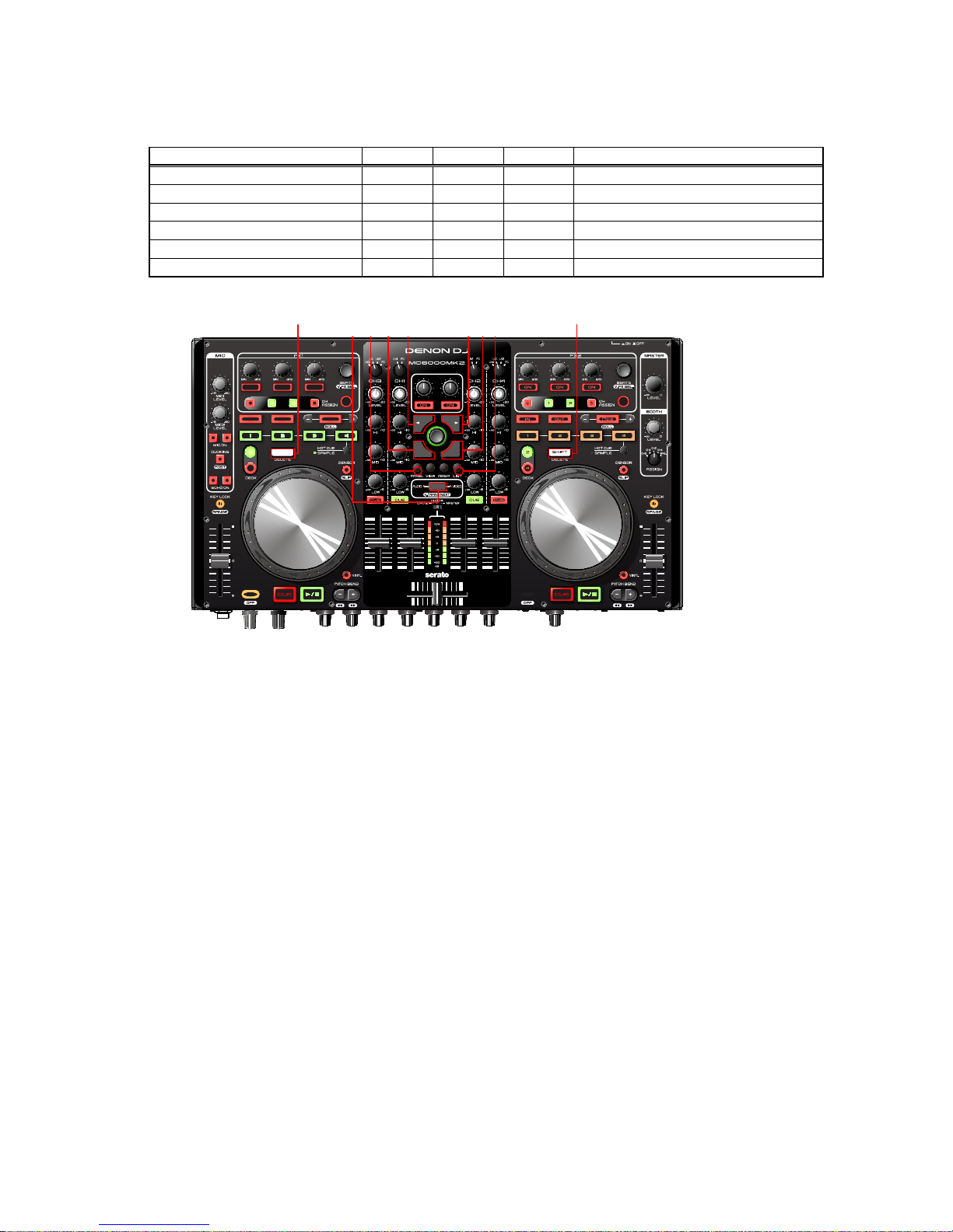
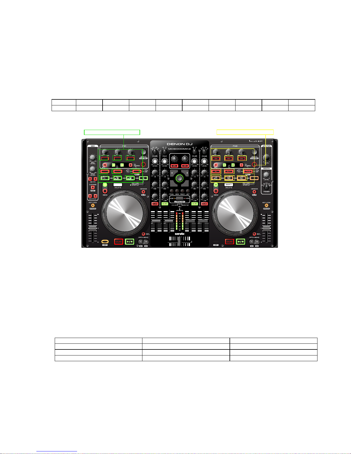
SPECIAL MODE
Special mode setting button
Hold down buttons A, B and C at the same time and press the power button to turn on the power.
Mode A B C Contents
Version Up mode 3 6 8 Firmware Upgrade
Version Display Mode 1 6 8 Firmware version display
Adjusting mode of the touch sense sensitivity 1 4 5 Adjust sensitivity of JOG wheel.
Initialize mode 1 3 6 Return to factory default setting.
MIDI transmission time mode 1 2 7 MIDI command transmission interval time
SW, VOLUME, ENCODER and LED TEST - - - Test of each function. (Use PC)
8
1 2 3 4 5 6 7
8
2. Version Up mode
Version up processing
*See "FIRMWARE UPDATE PROCEDURE" (34 page) for the procedure of the rmware update.
Page 24
24
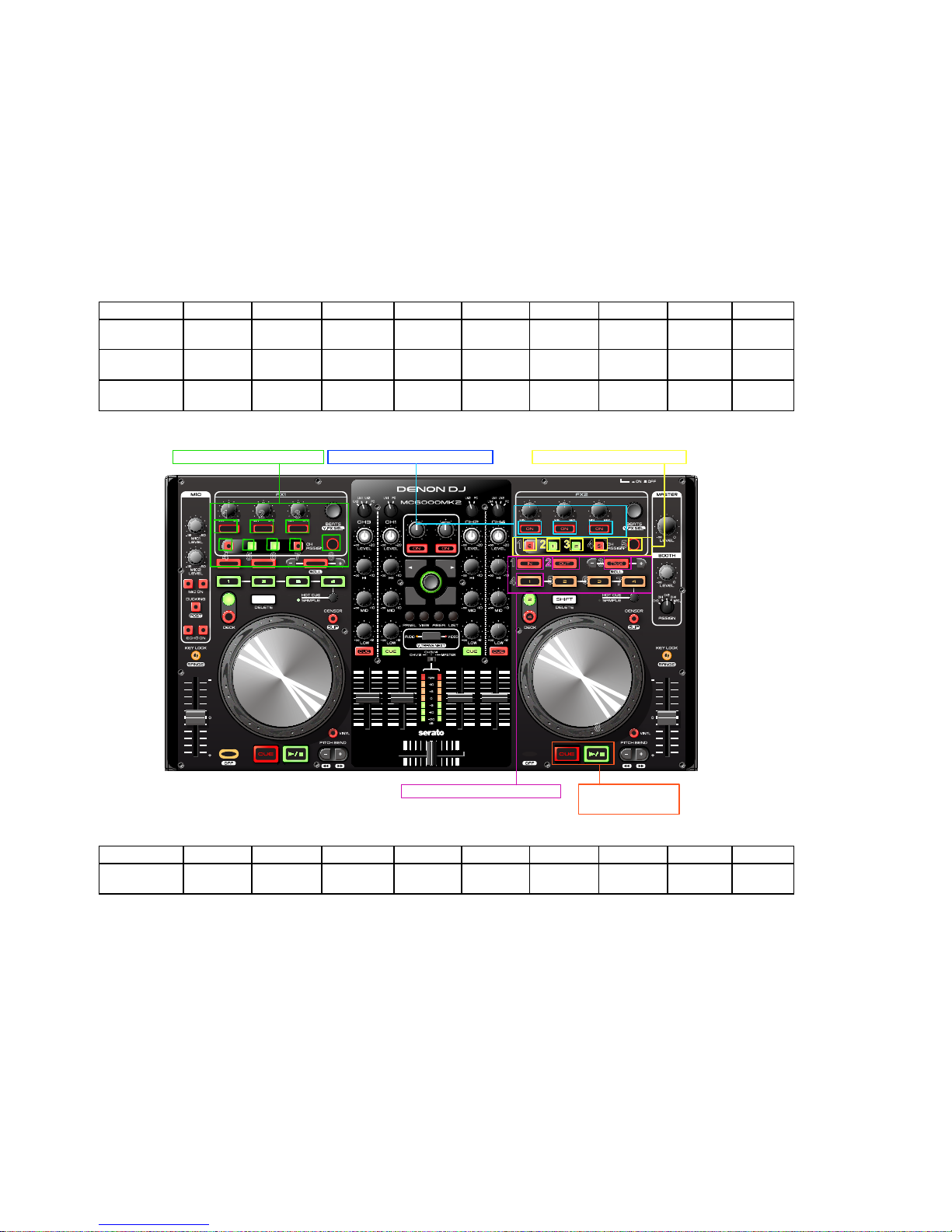
3. Version Display Mode
Displays the version of F/W or DSP.
Hold down buttons "SHIFT" "FWD"and "X-F LINK" at the same time and press the power button to turn on the power.
DSP version display by pressing the PLAY button.
F/W version display by pressing the CUE button.
Press [SHIFT] to return to Normal Mode.
How to read the version number
Firmware Version LED (Ver A.XYZ. After Ver1.000, it is commercial version).
A : LEFT DECK (for commercial version No.)
X, Y, Z : RIGHT DECK
1 2 3 4 5 6 7 8 9
A (LEFT
DECK)
FX1-L FX1-M FX1-R DECK3 DECK1 DECK2 DECK4 TAP -
X (RIGHT
DECK)
FX2-L FX2-M FX2-R - - - - - -
Y (RIGHT
DECK)
DECK3 DECK1 DECK2 DECK4 TA P - - - -
1 2 3 4 5 6 7 8 9
Z (RIGHT
DECK)
LOOP IN LOOP OUT AUTO LOOP HOT CUE1 HOT CUE2 HOT CUE3 HOT CUE4 - -
Example : Ver1.132
DECK A side : FX1-L.
DECK B side : FX2-L, DECK3, DECK1, DECK2, LOOP IN, LOOP OUT
Seven places of LED turns on.
1 2 3
4 5 86 7
1 2 3
1
65
7
8
1 2 3
4
2 3
A: The 1st digit numeric display. X: The 2nd digit numeric display.
Y: The 3rd digit numeric display.
Z: The 3rd digit numeric display.
54
CUE:System version
PLAY: DSP version
Page 25
25
4. Adjusting mode of the touch sense sensitivity
The unit can be controlled the sensitivity of the touch sensor for the Jog Wheel in 9 steps (-4 to 0 to +4).
“-4” is the lowest sensitivity, and “+4” is the highest sensitivity.
The default setting is “0”.
(1) Pressing (X-F LINK+LOAD A+LOAD B) at the same time, then turn on MC6000MK2.
(2) Press CUE, and switch the jog wheel that you want to adjust.
(e.g.)If you press CUE of the left side, only CUE of the left side turns on, and jog wheel of the left deck is chosen to
adjust it.
(3) Rotate the track selection knob, and adjust the sensitivity. The button lights according to the set sensitivity
Buttons HOT CUE 1 HOT CUE 2 HOT CUE 3 LOOP IN LOOP OUT AUTO LOOP FX1-L FX1-M FX1-R
Sensitivity -4 -3 -2 -1 0 1 2 3 4
(4) Press the track selection knob to memorize adjustment data.
(5) Press SHIFT, then the mode switches back from the sensitivity adjustment mode to the normal mode.
5. Initialization of parameters
Return to factory default setting.
(1) Pressing (BACK+FWD+X-F LINK) at the same time, then turn on MC6000MK2.
(2) Return to default setting, and these data (as follows) turn to factory default setting.
Upon completion of the adjustment, it automatically restarts, start in Normal mode.
Initialize Data Factory default Range
JW transmission interval time 4ms 3ms
<->
20ms
Sensitivity of JOG Wheel 0 -4
<->
4
Filter/Video mode Filter Filter
<->
Video
-1
2 3 4
0 1
-2
2 3
-1
8
0
1
Left deck
Right deck
4
-3
-4
-4
-2-3
Page 26
26
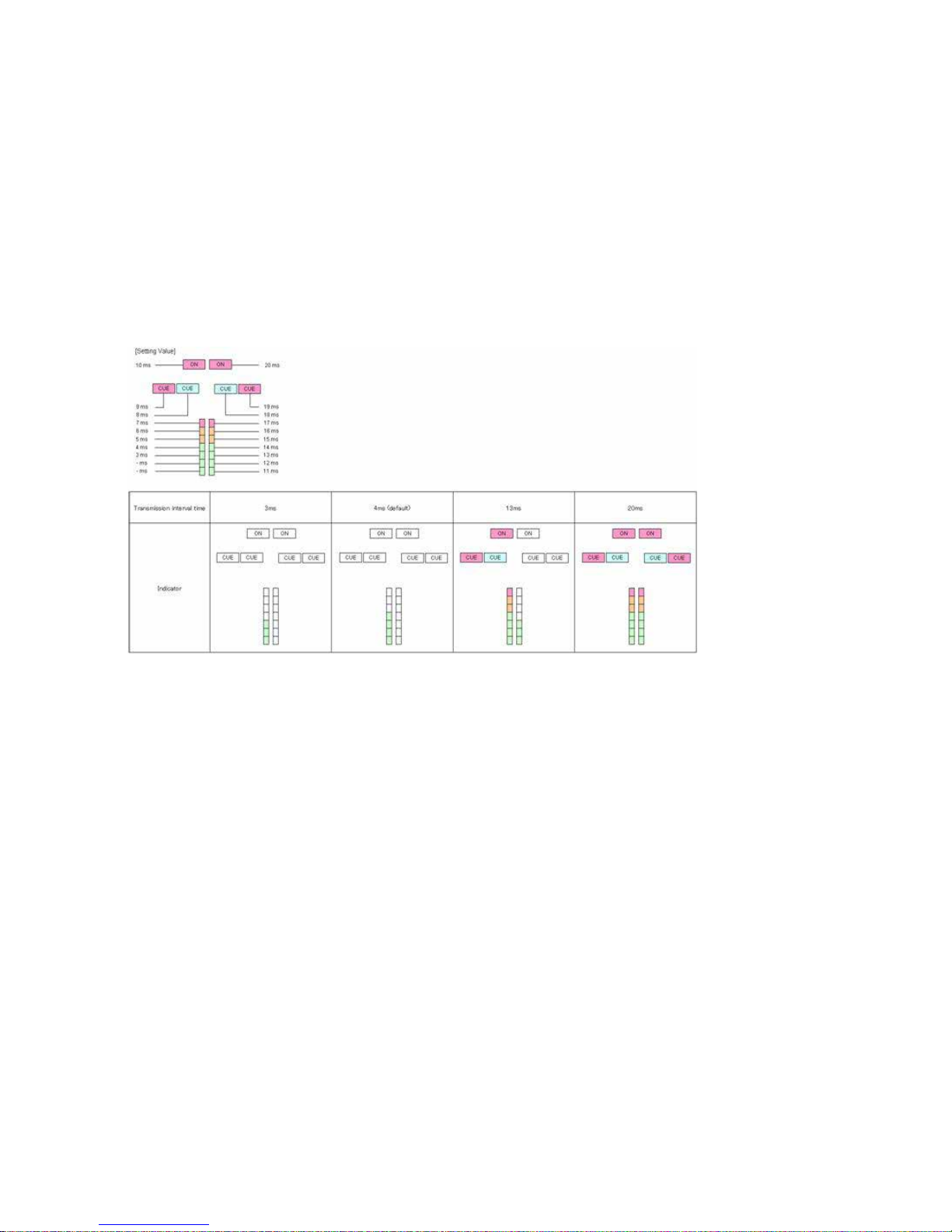
6. Adjusting interval time of MIDI command transmission
Depending on the computer specications and OS type, the computer may not be able to receive the MIDI commands
transmitted from this unit correctly.
In this case, use the following operation to set the MIDI command transmission interval time to a suitable value.
(1) Pressing (PANEL+LIST+X-F LINK) at the same time, then turn on MC6000MK2.
The following LED turns on, and the unit switches to the setting mode for MIDI command transmission interval time.
(2) Rotate SEL.
The relationship between LED display position and the MIDI command transmission interval time is as shown in the
diagram as follows. The factory setting is 4 msec.
(3) Press SEL.
The MIDI command transmission interval time is entered.
(4) Press SHIFT.
The settings are completed, and unit exits the setting mode.
How to read the interval time
Page 27

27
7. SW, VOLUME, ENCODER and LED TEST
Operating check procedure for the SW/VOLUME/ENCODER and LEDs on this unit with MIDI-OX.
[1] MIDI-OX Installation and Settings
Install MIDI-OX on the PC, and congure the PC environment.
(1) Download MIDI-OX (freeware).
Download from the URL below.
URL: www.midiox.com/
(2) Install MIDI-OX on the PC.
(3) Connect this unit to the PC, and switch the power on.
(4) Start MIDI-OX that you installed on the PC.
(5) In MIDI-OX, select [View] menu - [Input Monitor].
(6) Select [Window] menu - [Tile Horizontally].
Page 28

28
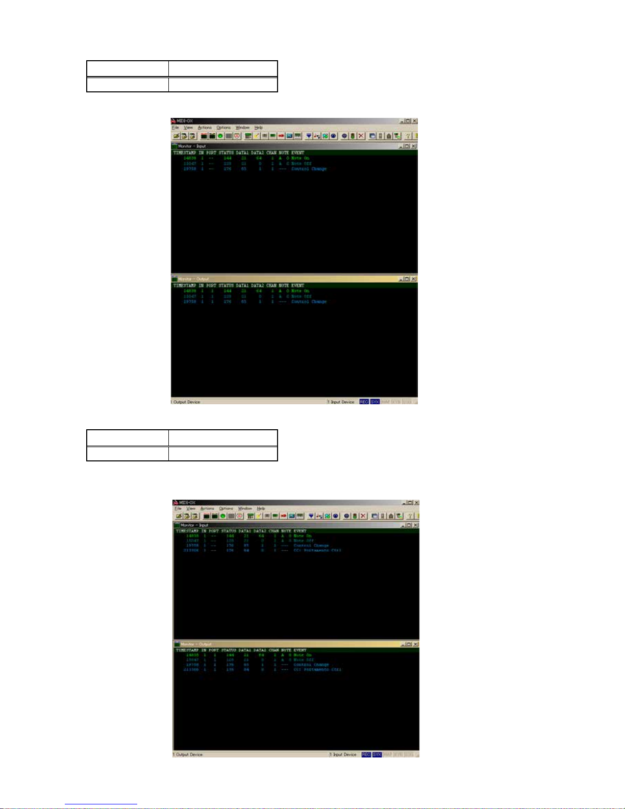
(7) Open the [Actions] menu and check that “Stop Display” is shown.
If “Start Display” is shown, click “Start Display” so that “Stop Display” is shown.
[2] Check the SW/VOLUME/ENCODER
When SW/VOLUME/ENCODER is operated on this unit, the corresponding MIDI command is shown on MIDI-OX.
If the MIDI command is not shown on MIDI-OX even when the panel of this unit is operated, check the following.
(1) Select [Options] menu - [MIDI Device].
Page 29
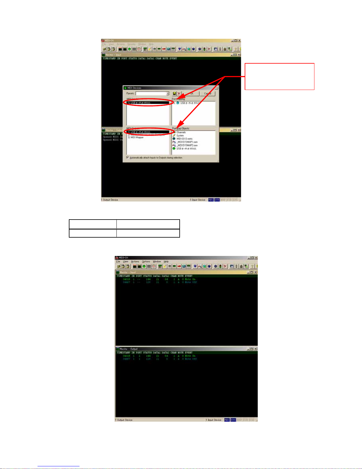
29
(2) Check whether the USB audio device is selected.
(3) Screen display when the EFX.1 button on this unit is switched ON-OFF.
Pressed button DATA1 column display
EFX.1 (FX1) 21
For details on the correspondence between operation on this unit and the contents of the screen display, see the
"MIDI command list" in the instruction manual.
Check that it is highlighted black.
If it is not highlighted, select it
so that it is highlighted black.
Page 30
30
(4) Next, this is the screen display when the EFX.1 knob is moved either to the left or right.
Operated knob DATA1 column display
EFX.1 85
For details on the correspondence between operation on this unit and the contents of the screen display, see the
"MIDI command list" in the instruction manual.
(5) Next, this is the screen display when the TRACK SELECT knob on the unit is moved 1click to the right.
Operated knob DATA1 column display
TRACK SELECT 84
For details on the correspondence between operation on this unit and the contents of the screen display, see the
"MIDI command list" in the instruction manual.
Page 31

31
[3] Check the LED
When the MIDI command is sent from MIDI-OX, the LED lights/ashes/off/Dimmer.
(1) Select [View] menu - [Control Panel].
(2) These are explained in order of LED lights/off/ashes/Dimmer.
Example1 : When lighting the EFX.1 button on DECK A
In the MIDI-OX Control Panel, set the following parameters.
Control Event Channel Value
74) Brightness 1 92
When the Enter button on the PC keyboard is pressed, the EFX.1 button on the unit lights.
Page 32

32
Example2 : When ashing the EFX.1 button on DECK A
In the MIDI-OX Control Panel, set the following parameters.
Control Event Channel Value
76) --- 1 92
When the Enter button on the PC keyboard is pressed, the EFX.1 button on the unit ashes.
Example3 : When off the EFX.1 button on DECK A
In the MIDI-OX Control Panel, set the following parameters.
Control Event Channel Value
75) -- 1 92
When the Enter button on the PC keyboard is pressed, the EFX.1 button on the unit off.
Page 33

33
Example4 : When dimming the EFX.1 button on DECK A
In the MIDI-OX Control Panel, set the following parameters.
Control Event
Channel
Value
74) Brightness 1 44
When the Enter button on the PC keyboard is pressed, the EFX.1 button on the unit dims.
b
Some of the LEDs such as those for Meter or Ducking use the following parameters to light/switch off.
Control Event
Light
80) ---
Off 81) ---
For details, see the “MIDI command list” in the instruction manual.
Page 34

34
PROCEDURE AFTER REPLACING THE MICROPROCESSOR, ETC
The procedure after replacing the u-COM (Microprocessor), ash ROM, etc. is as follows.
PWB
Name
Ref. No. Description
After
replaced
Remark
CONTROL
IC100 STM8S207M8T6 B 704-6K2-A620
CONTROL
IC105 IC(EN25F1-100GIPTR) B 417-DDJLE-1084
After replacing
A : The software has been written. The software is not written at the time of replacement.
B : The software has been written. The software may need to be rewritten by version updates. Check the version.
C : The software has not been written. The software needs to be written after replacement. See “Firmware Update
Procedure” for information on writing the software.
D : The software has been written. Be sure to rewrite with the latest software for your service region. See “Firmware
Update Procedure” for information on writing the software.
FIRMWARE UPDATE PROCEDURE
1. Items to Be Prepared
(1) Connect the computer by USB cable.
MC6000MK2 : Type B
(2) UPDATER
Dowload Dennon SDI site.
for Windows : DDJUpdater-2.0.msi
for Mac : DDJ Updater.app
(3) Latest Firmware
Dowload Dennon SDI site.
le : MC6000MK2_vX.YYY
(X.YYY: Ver.No.)
2. InstallingthermwareupdateprogramforWindows
b
Upgrade program for Macintosh is installed on your Mac by copied the DDJ Updater.app.
(1) Double click the DDJUpdater-2.0.msi
MC3000
Page 35

35
(2) Click the Next.
(3) Check the I accept the terms of the license agreement,and Click the Next.
(4) Click the Next.
Page 36

36
(5) Click the Next.
(6) Click the Next.
(7) The Setup Status bar appears.
Page 37

37
(8) Click the Close.
3. UpdateFirmware
[Caution]
During the loading and upgrading the power OFF and set, PC or please do not remove the cable connection.
Also, please press the button of a keyboard and computer sets.
(1) Connect the USB cable from PC to the unit.
(2) Press the POWER button to turn on while pressing buttons BACK, FWD and SHIFT.
(3) MC6000MK2 will enter versionup mode. CUE 1 will light.
(4) Run the "DDJ Updater” on desktop of PC.
M6000MK2
Page 38

38
(5) Click the File menu. And click the Open. Select the latest rmware.
(6) Click the Load.
MC6000MK2
MC6000MK2
MC3000
MC6000MK2
Page 39

39
(7) The Setup Status bar appears.
(8) Click the OK.
MC6000MK2
MC3000
MC6000MK2
MC6000MK2
Page 40

40
(9) Click the Execute.
(10) The Setup Status bar appears.
MC6000MK2 indicates state of updating.
CUE 1: Update Ready, CUE 2: Update Data(0%),
CUE 3: Update Data(50%), CUE 4: Update Data(100%)
MC6000MK2
MC6000MK2
MC6000MK2
MC6000MK2
Ver.1.100
Page 41

41
(11) Click the OK.
(12) When version up nished, this unit is usual mode automatically.
Failure to upgrade to the PC "Version up was not completed." is displayed.
Then "Execute" click again.
MC6000MK2
Page 42

42
4. Errormessage&trabuleshooting
Message Solution
File is invalid. Please select the update le for this unit.
Load failed. Check the connection, and retry Please try again step (1).
Loaded data is invalid. Check the le Please select the update le for this unit.
Version up was not completed Please try again step (1).
(1) Unit is not connected or if the unit is not upgraded mode as shown below. Please try again step (1).
(2) If the le version is not loaded "File is not ready." Is displayed. Please try again step (5).
[Caution]
During the loading and upgrading the power OFF and set, PC or please do not remove the cable connection. Also, please
press the button of a keyboard and computer sets.
MC6000MK2
Page 43

43
TROUBLE SHOOTING
1. FLOW CHART NO.1 (704-6K2-A617 : MAIN PCB ASS'Y)
FLOW CHART NO.2 (704-6K2-A617 : MAIN PCB ASS'Y)
The unit does not power on
Has a fuse broken?
Are the FFC(24 pin:CN102), FFC(20 pin:CN801),
and PH(6 pin:CN1) correctly connected?
Is a voltage of +5V supplied to 7 pin of IC100(CPU)?
Replace IC100.
See FLOW CHART NO.2 <Broken fuse>.
Connect the connectors correctly.
NO
NO
NO
YES
YES
YES
Broken fuse
Are +12V, D5V and D3.3V voltage line supply being correctly?
Replace the fuse after repair.
Replace any faulty parts.
NO
YES
Check the circuits around the IC100 and replace any faulty
parts. (L1, SW1, Q1, L5, IC2, L7, L4, IC105)
Page 44

44
FLOW CHART NO.3 (704-6K2-A617 : MAIN PCB ASS'Y)
FLOW CHART NO.4 (704-6K2-A617 : MAIN PCB ASS'Y)
D3.3V is not outputted
Is +12V voltage line supply being correctly?
NO
D5V is not outputted
Is +12V voltage line supply being correctly?
Check the circuits around the IC1 and replace any faulty
parts.
See FLOW CHART NO.2 <Broken fuse>.
NO
YES
FLOW CHART NO.5 (704-6K2-A618 : IO PCB ASS'Y)
A5V is not outputted
Is +12V voltage line supply being correctly?
Check the circuits around the Q40 and replace any faulty
parts.
See FLOW CHART NO.2 <Broken fuse>.
NO
YES
See FLOW CHART NO.2 <Broken fuse>.
YES
Check the circuits around the IC2 and replace any faulty
parts.
Page 45

45
FLOW CHART NO.6 (704-6K2-A618 : IO PCB ASS'Y)
FLOW CHART NO.7 (704-6K2-A618 : IO PCB ASS'Y)
+A12V is not outputted
Is +12V voltage line supply being correctly? See FLOW CHART NO.2 <Broken fuse>.
NO
YES
Check the circuits around the Q41 and replace any faulty parts.
-A12V is not outputted
Is +12V voltage line supply being correctly?
Check the circuits around the U741 and replace any faulty
parts.
See FLOW CHART NO.2 <Broken fuse>.
NO
YES
FLOW CHART NO.8 (704-6K2-A618 IO PCB ASS'Y)
A3.3V is not outputted
Is +12V voltage line supply being correctly?
Check the circuits around the U40 and replace any faulty
parts.
See FLOW CHART NO.2 <Broken fuse>.
NO
YES
Page 46

46
FLOW CHART NO.9 (704-6K2-A615 CONRTOL 1 PCB ASS'Y)
NO
NO
The keys cannot be operated
Are the contact point and the installation state of the key
switches (SW100~SW170) and rotary encoder (SW150, 154,
158) nomal?
Does LED (D153~D180, D207~D287) light correctly?
When pressing each key switches, turning rotary switches
and turning rotary encoder, does the voltage of each pin of
IC100 (shown below) decrease?
-------------------------------------------------------------------------------SW100, SW106, SW111, SW116, SW121, SW126, SW131,
SW136, SW141: IC100 60pin
SW101, SW109, SW114, SW119, SW124, SW129, SW134,
SW139, SW144: IC100 61pin
SW102, SW108, SW113, SW118, SW123, SW128, SW133,
SW138, SW143: IC100 62pin
SW103, SW105, SW110, SW115, SW120, SW125, SW130,
SW135, SW140: IC100 63pin
SW104, SW107, SW112, SW117, SW122, SW127, SW132,
SW137, SW142: IC100 64pin
SW147, SW153, SW157, SW162, SW166, SW167, SW168,
SW169, SW170: IC100 65pin
SW148, SW151, SW155, SW159, SW163: IC100 66pin
SW149, SW152, SW156, SW160, SW164: IC100 67pin
SW161, SW165: IC100 70pin
Rotary encoder
SW150, SW154, SW158: IC100 70pin
Re-paste the switches correctly or replace the poor switches.
YES
YES
YES
Check the Q100~Q120, IC101, IC102, IC107 and surrounding,
and replace any faulty parts.
NO
Check the key switches and the rotary encoder and and
surrounding, and replace any faulty parts.
YES
Replace IC100.
Page 47

47
NO
Slide switches cannot be operated.
Are the contact point and the installation state of the Slide
switche (SW174) normal?
When switching Slide switch (SW174), does the voltage of 11
pin of IC109 increase?
Re-paste the switches correctly or replace the poor switches.
YES
FLOW CHART NO.10 (704-6K2-A615 CONRTOL 1 PCB ASS'Y)
FLOW CHART NO.11 (704-6K2-A616 CONRTOL 2 PCB ASS'Y)
The keys cannot be operated
Is the FFC(CN100) correctly connected ?
Are the contact point and the installation state of the key
switches (SW400~SW411) nomal?
YES
NO
Connect the FFC correctly.
NO
Check A3.3V is output.
YES
Replace IC109.
NO
Re-paste the switches correctly or replace the poor switch.
YES
Does LED (D412~D431, D434~D445 ) light correctly?
NO
Check the Q403~Q414, IC401 and surrounding, and
replace any faulty parts.
When pressing each key switches, turning rotary switches
and turning rotary encoder, does the voltage of each pin of
IC100 (shown below) decrease?
-----------------------------------------------------------------------------SW400, SW401, SW402, SW403: IC100 66pin
SW404, SW406, SW408, SW410: IC100 67pin
SW405, SW407, SW409, SW411: IC100 70pin
Replace IC100.
YES
YES
NO
Check the key switches and the rotary encoder and and
surrounding, and replace any faulty parts.
Page 48

48
FLOW CHART NO.12 (704-6K2-A618 IO PCB ASS'Y, 704-6K2-A617 : MAIN PCB ASS'Y)
Audio is not output from the Master output.
Are the PH(6pin:CN1), FFC(24pin:CN102), and
FFC(20pin:CN801) correctly connected?
YES
• Set the channel input source switch to "LINE"
• Set the CROSS FADER CONTOUR to "THRU"
• Set the input level volume to "12:00"
• Set the Cannel FADER to "MAX".
• Set the master level volume to "14:30".
Are audio signals output to 18pin(Lch), 15pin(Rch) of U755
when an audio signal of 1kHz 0dBV is input externally to the
LINE input?
Are the audio signals outputted to 7 pin(Lch), 1 pin(Rch) of
U507?
Are the audio signals outputted to 7 pin(Lch), 1 pin(Rch) of
U508?
Check surrounding circuit of JK504, JK505 from 1 pin(Rch), 7
pin(Lch) of U508, and replace any faulty parts.
Is base terminal of Q42(MUTE control signal) +3.3V, and has
been base terminal of Q518~Q521(MUTE drive signal) L
(-12V)?
YES
YES
YES
YES
NO
Connect the connector cable and FFCs correctly.
NO
Check surrounding circuit of U755, and service it if defective.
When the surrounding circuit is correct, replace U755.
NO
Check surrounding circuit of U507, and service it if defective.
When the surrounding circuit is correct, replace U507.
NO
Check surrounding circuit of U508, and service it if defective.
When the surrounding circuit is correct, replace U508.
NO
Check surrounding circuit of Q42, Q518~Q521 and replace
any faulty parts.
Page 49

49
FLOW CHART NO.14 (704-6K2-A616 CONRTOL 2 PCB ASS'Y, 704-6K2-A615 CONRTOL 1 PCB ASS'Y)
JOG WHEEL is no operating
(BEND functions is not operating)
Is D3.3V being output from 27 pin of CN100?
Is encoder waveform(0-3.3V) outputted to 14pin, 15pin, 16pin,
17pin of CN100, when JOG WHEEL is turned.(See Fig.1-6 of
the 52 page.)
Is encoder waveform(0-3.3V) outputted to 9pin, 10pin, 11pin,
12pin of IC100 from CN100, when JOG WHEEL is turned.(See
Fig.1-6 of the 52 page.)
Connect the FFC (32pin:CN100) correctly.
Check surrounding circuit of CN100 from D432/D433/D443/
D444, and service it if defective.When the surrounding circuit
is correct, replace FFC cabel.
NO
NO
YES
YES
FLOW CHART NO.13 (704-6K2-A618 IO PCB ASS'Y, 704-6K2-A617 : MAIN PCB ASS'Y)
Sound of LINE input is not being output correctly
Are the PH(6pin:CN1), FFC(24pin:CN102), and
FFC(20pin:CN801) correctly connected?
YES
• Set the channel input source switch to "LINE"
• Set the CROSS FADER CONTOUR to "THRU"
• Set the input level volume to "12:00"
• Set the Cannel FADER to "MAX".
• Set the master level volume to "14:30".
Are audio signals output to 7pin(Lch), 1pin(Rch) of U505
when an audio signal of 1kHz 0dBV is input externally to the
LINE input?
Are the audio signals outputted to 11 pin and 12 pin of U751?
Are the digital audio signals (0-3.3V) outputted from 4 pin of
U751?
Check surrounding circuit of 88 pin of IC902 from 4 pin of
U751, and replace any faulty parts.
YES
YES
YES
NO
Connect the connector cable and FFCs correctly.
NO
Check surrounding circuit of U505 from K500, and service it if
defective.
When the surrounding circuit is correct, replace U505.
NO
Check periphery circuit of U751 from U505, and replace any
faulty parts.
When the periphery circuit is correct, replace U751.
NO
Replace any faulty parts.
NO
Check surrounding circuit of IC100 from CN100, and service it
if defective.
YES
Replace IC100.
Page 50

50
FLOW CHART NO.15 (704-6K2-A615 CONRTOL 1 PCB ASS'Y)
JOG WHEEL is not operating
(SCRATCH function is not operating)
Is BEND function operating?
YES
Is reference waveform outputted at 2pin, 6pin and 12pin of
IC106 and IC111?
(See Fig.1-7-1 of the 52 page.)
When JOG WHEEL is touched, is wavelength of 2pin, 6pin
and 12pin changing of IC106 and IC111?
(See Fig.1-7-2 of the 52 page.)
Is waveform inputed to 2pin of IC104 and 5pin of IC110?
(See Fig.1-7-3 of the 52 page.)
Replace IC100.
When the top of JOG WHEEL is touched, is waveform inputed
to 20pin and 28pin of IC100 changed?
YES
YES
YES
YES
NO
See FLOW CHART NO.14 <JOG WHEEL is not
operating. (BEND function is not operating.)>.
NO
Check the surrounding circuit of IC106 and IC111 and rreplace
any faulty parts.
When the surrounding circuit is correct, replace IC106 and
IC111.
NO
Check the surrounding circuit of JOG WHEEL form IC106
and IC111 and replace any faulty parts When the surrounding
circuit is correct, replace JOG WHEEL.
NO
Replace IC104 and IC110.
NO
Check surrounding circuit of IC100 from IC104 and IC110,
and replace any faulty parts.When the surrounding circuit is
correct, replace IC104 and IC110.
Page 51

51
WAVEFORMS and TROUBLESHOOTING
1-1 Power failure
Symptom: The DECK1&2 LED and DECK1&2 VINYL does not light. Status of
The product: The power circuit failure
Diagnostic procedure:
1. Connect the DC12V/3A adaptor, Turn on the power switch, as gure 1-1.
2. Check each DC voltage, measure C21 positive to ground is +12V C18 positive to ground is D5V, C17 positive to ground is D3.3V, C46
positive to ground is 3.3V, C47 positive to ground is A3.3V, C51 negative to ground is A-12V, C50 positive to
ground is A+12V.
1-2Nokeyfunction
Symptom: No key function
Diagnostic procedure:
1.Measure if there is operating wave for pin of tact sw, as gure 1-2
If it is not, please check tact sw. status.
1-3 Rotary selector not controllable
Symptom: Rotary selector not controllable
Diagnostic procedure:
1.Measure if there is operating wave for pin of EN1~EN6, Check IC100 PIN42 ~ PIN46&PIN52,
as gure 1-3
If it is always on high level, please check if Rotary selector is controlled.
1-1 C21 +12V
1-3 ROTARY ENCODER PIN
1-2 TACT SW PIN
1-1 C50 A+12V1-1 C51 A-12V1-1 C47 A3.3V
1-1 C46 3.3V1-1 C17 D3.3V1-1 C18 D5V
Page 52

52
1-4Slidervolumenotcontrollable
Symptom: Slider volume not controllable
Diagnostic procedure:
1.Measure if there is operating wave for pin of AD10~AD11, Check IC402 PIN3&PIN13, as gure 1-4
If it is always on high level, please check if Rotary selector is controlled.
1-5Selectswitchcannotwork
Symptom: Select switch can not work
Diagnostic procedure:
1.Measure if there is operating wave for pin, Check IC380 PIN9&PIN10, as gure 1-5
If it is always on high level, please check if selector switch is controlled.
1-6 Jog rotation can not be dectected
Symptom: Jog rotation can not be detected
Diagnostic procedure:
1.Turn the jog to measure if there is operating wave for pin, Check IC403 PIN2&PIN4&PIN8&PIN10, as gure 1-6
1-7Jogtouchcannotbedetected
Symptom: Jog touch can not be detected
Diagnostic procedure:
1.Touch the jog to measure if it is Hi to Low for pin, Check IC106&IC111 PIN5, as gure 1-7-4
If the wave is unexpected, please check IC106&IC111
1-6 JOG ROTATION PIN
1-5 SLIDER SWITCH PIN
1-4 SLIDER VOLUME PIN
1-7-31-7-21-7-1
1-7-4
Page 53

53
1-8Nosoundinput/outputfromUSB
Symptom: Audio is not input/output :
Diagnostic procedure:
1.Connect PC with USB cable.
2.Is there clock 6MHz to ground IC901->PIN51&50 If it is not, IC901、X900 is damaged.
3.Is a signal input to the USB D+ & D- ? IC901 USB IN->PIN7& PIN8 , as gure 1-8
4.If it is not, IC901 is damaged.
1-9NosoundoutputfromMASTEROUT
Symptom: Audio is not output & MASTER level meter is not light up :
Diagnostic procedure:
1.Is a signal output to the DAC? U755:MASTER->PIN15&PIN18
A. If it is, something is wrong with the analog -circuit block. Check if output amplier (U515:MASTER) is
working normally. Check if each MUTE transistor (Q512~513) BASE PIN is -12V.
B. If it is not, something is wrong with the digital-circuit block. Check if there is CLOCK signal for
U755 :MASTER->PIN1 & PIN2 & PIN3 & PIN4 , as gure 1-9.
1-10NosoundoutputfromBOOTH
Symptom: Audio is not output :
Diagnostic procedure:
1. Is a signal output to the DAC? U756:BOOTH->PIN15 & PIN18
A. If it is, something is wrong with the analog -circuit block. Check if output amplier (U510)
is working normally. Check if each MUTE transistor (Q526~Q529) BASE PIN is -12V.
B. If it is not, something is wrong with the digital-circuit block. Check if there is CLOCK signal for
U756:BOOTH ->PIN1 & PIN2 & PIN3 & PIN4, as gure 1-9.
1-9 U755 PIN 21-9 U755 PIN 1
1-8 IC901 PIN7& PIN8
1-9 U755 PIN 4
1-9 U755 PIN 3
Page 54

54
1-11NosoundoutputfromPHONES
Symptom: Audio is not output :
Diagnostic procedure:
1. Is a signal output to the DAC? U759:PHONES->PIN15 & PIN18
A. If it is, something is wrong with the analog -circuit block. Check if output amplier (U512: PHONES) is
working normally. Check if each MUTE transistor (Q550~Q553:PHONES)BASE PIN is -12V.
B. If it is not, something is wrong with the digital-circuit block. Check if there is CLOCK signal for
U759 :PHONE->PIN1 & PIN2 & PIN3 & PIN4, as gure 1-9.
1-12NosoundinputfromMIC1
Symptom: Audio is not input:
Diagnostic procedure:
1. Is a signal input to the ADC ? MIC(U752) ->PIN10
A. If it is not, something is wrong with the analog-circuit block. Check if OPA MIC(U513) is working
normally.
B. If it is, something is wrong with the digital-circuit block. Check if there is CLOCK signal for MIC(U752) >PIN2 & PIN4 & PIN7 & PIN8, as gure 1-9
1-9 U755 PIN 21-9 U755 PIN 1
1-9 U755 PIN 4
1-9 U755 PIN 3
Page 55

55
BLOCK DIAGRAM
LINE1 L/R
LINE3/PHONO
L/R
0dBV
(-40dBV)PHONO
-11.48dB
ADC
CS5341
-16.93dB
ADC
PCM1803
LINE4/PHONO
L/R
(-40dBV)PHONO
LINE2 L/R
0dBV ADC
CS5341
2
3
1
L
T
R
R
G
S
MIC1
MIC2
-40dBu
-40dBu
Balance(mono)
Balance(mono)
ADC
CS5341
+40dB
+40dB
+12.25dB
DAC
CS4351
MASTER OUT(RCA)
BAL ANCE
+4dB
2
3
1
MASTER OUT(Balance)
+12.25dB
BAL ANCE
+4dB
BOOTH OUT(Balance)
L
3
R
2
G
1
+4.19dB
REC OUT(RCA)
+16.9dB Headphone(40 ohm)
L
3
R
2
G
1
NJM8080G
NJM8080G
NJM8080G
NJM8080G
NJM8080G
NJM8080G
NJM8080G
NJM8080G
NJM8080G
NJM8080G
NJM8080G
NJM2068
NJM8080G
DSP56724
FLASH ROM
EN25F10
USB PortB
TUSB3200
DC POWER
+12V/3A
STM8S207MBT6
MCU
1 2
POWER
MOSFET SW
TPS54232
TPS54232
D3.3V
D5V
A+12V
SPI
I2C
EXT. AD
TC4052*6
CROSS* 1
PITCH* 4
FADER* 4
ROTARY* 28
FUNCTI ON*4
PIC16F616*2
PWM
TOUCH PLAT* 2
ENCODER* 6
LED* 152
DI0 DI1
DI2
DI3
DI4
DI5
DI6
DO0 DO1
DO2
DO3
DO4
DO5
URST
DRST
6M
512fs for A/D,D/A)
(I2S format for audio data)
(245.76MHz)
24.576M
(12MHz)
(24MHz )
Switching P ower
Front PCB
I/O PCB
Control PC B
-16.93dB
NJM8080G
-11.48dB
NJM8080G
BCK
ST/MO SW*1
WHEEL *4
EXT. AD
TC4052*2
Booth EQ*2
MIC EQ*6
Front PCB
TPS54232A5V
XFADER* 1
CH SW*4
MIC ECHO*1
Monitor*2
12pAD
4pAD
Split Cue*1
USB Audio*1
Tact/Push SWsend
*81
return9p9p
Hysteresis
74HC14
RIAA
2C11
LN/PH
RIAA
2
C1
1
LN/PH
MUTE
MUTE
MUTE
MUTE
MUTE
MUTE
MUTE
LRCK
BD4745
A+12V
A-12V
Compare
Power Delay
Buck boost
Buck
Buck
KTC3228Y
ADC
PCM1803
D3.3VA5V
D3.3VA5V
D3.3VA5V
D3.3VA5V
D3.3VA5V
D3.3VD5V
D3.3V
D3.3V D5V
D5V
D3.3V
DAC
CS4351
DAC
CS4351
DAC
CS4351
SER.- ->PAL.
74HCT595*5
D3.3V
D5V
USB SW.
D3.3VA+12V
Tr. AMP
3 1
2
+16.39~ +60 dB
NJM2068
3 1
2
+16.39~ +60 dB
-11.48dB
-11.48dB
Tr. Buffer
Tr. Bufer
I2S Buffer
74HC4050
BCK ,LRCK
SCK
24M
MAIN PCB
I/O PC B
MAIN PCB
2SA2127
2SD1207S
A+12V
MTZJ6.8B
A3.3V
BU33TD3
A3.3V
LDO
D3.3VA+12VA3.3V
D3.3VA+12VA3.3V
D3.3VA+12VA3.3V
INT
Page 56

56
POWER BLOCK DIAGRAM
A
B
C
D
AC/DC Adapertor
+12V/3A
MOSFET SW
TPS54232
AC IN
Main Power Cont.
A+12V
Buck Boost
DC Convertor
A-12V
Pre-OPA
NJM8080G
Phones Driver
LDO
BU33TD3
DAC
CS4351
A. Mute
2SD2704K
DC/DC Buck
TPS54232
D5V
D3.3V
DC/DC Buck
TPS54232
DC Convertor
USB Controller
TUSB3200 logic
USB Controller
TUSB3200 Core
AD Switch
Flash Memory
EN25F10
LED Scan
74HCT595
Hysteresis
74HC14
POWER BLOCK DIAGRAME
74HC4052
ADC
CS5341
ADC
PCM1803
MCU
STM8S207
PWM
PIC16F616
DAC
CS4351
DC Convertor
LDO
NJM79L09
MIC-OPA
NJM2068
A-9V
Phones Driver
Pre-OPA
NJM8080G
DAC
CS4351
LDO
KTC3228Y
ADC
CS5341
ADC
PCM1803
A5V
A3.3V
A. Mute
2SD2704K
2SC1815GR
2SA1015GR
MIC-OPA
NJM2068
A-12V
D5V
D3.3V
Page 57

57
LEVEL DIAGRAM
Line3,4/Phono
-17.5
A/D
dBV
LINE Max Input Level
0
10
20
-10
-20
-30
-40
-50
-60
-70
-80
-90
-100
-110
-120
-130
limit -0.1dBV
PCM1803
dBV
0
10
20
-10
-20
-30
-40
-50
-60
-70
-80
-90
-100
-110
-120
-130
dBFS
ANALOG
31
2
TRIM EQ
31
2 3
1
2
CH.Fader * CR.Fader
0
-10
-20
-30
-40
-50
-60
-70
-80
-90
-100
-110
-120
-130
DR:105dB
-140
dBV
0
10
20
-10
-20
-30
-40
-50
-60
-70
-80
-90
-100
-110
-120
-130
D/A
DR:112dB
CS4351
0dBFS=6dBV
31
2
Master Level
NJM8080G
Master Out
ANALOG
DIGITAL
DR:112dB
-16.93
NJM8080G
15dBV
CS5341
+6
231
NJM8080G
dBV
0
10
20
-10
-20
-30
-40
-50
-60
-70
-80
-90
-100
-110
+10.24
BALANCE Max. 23.6dBu
+8~ -12 dB
-144dBFS@24bit
Noise Level
PC-->DA@-77.76dBV
@-121dBV
Clip=17.41dBV
Clip=17.41dBV
Balance Clip=23.41dBV
MIC VR Min. position
-16dBu
+16.39
-60dBu
Phono Level
-40dBV
+40
D/A
DR:112dB
CS4351
0dBFS=6dBV
31
2
CUE Level
+11.9
Mic. Max. Noise -68.36dBV
Unbalance Max. 19.6dBu
L
3
R
2
G
1
PHONES
RIAA
LN:0
PH:+40
+20~0~ -∞ dB
+10~ -∞ dB
0~ -∞ dB +10~ -∞ dB
LINE1,2
A/D
limit -0.1dBV
CS5341
-17.5
NJM8080G
NJM8080G
ADC
CS5341
L
3
R
2
G
1
S
4
MIC.
NJM2068
-17.5
NJM8080G
EQ
+15~ -15 dB
31
2
GAIN
+16.39~ +60 dB
Booth EQ
+15~-15dB
PCM1803
D/A
DR:112dB
CS4351
0dBFS=6dBV
31
2
Booth Level
NJM8080G
+10~ -∞ dB
XLR
RCA
+8
-12
+10.24
+15
Phones Max. 120mW
Phono Noise
-97.93dBV
Phono@-82.76dBV
0
-10
-20
-30
-40
-50
-60
-70
-80
-90
-100
-110
-120
-130
dBFS
+10.24
MIC Noise(VR.Min.)
@-127dBu
Max.Phono Level
-25dBV
Max. MIC Level 3dBu
DR:105dB
DR:103dB
DR:105dB
1:30 position
+20
Unbalance Out 0.45dBu(Ref.)Reference LINE3/4 level 0dBV
-15
MIC VR Max. position
+60
LINE1/2
LINE3/4
-16.93
CS5341
-17.5
15.05dBV
L
3
R
2
G
1
Booth Out
+6
-5dBFS
+10.24
-20dBFS
-40dBu
MIC VR 2:30 position
LINE1,2@-86.76dBV
Max. position
+10
Tr. AMP
limit +0.5dBV
+11.9
MIC
-17.5
-0.2dBFSMIC Max. IN
-16.93
+40
PCM1803
DR:103dB
LINE1/2 Noise
-132.48dBV
MIC Noise(VR.Max.)
MIC Noise(VR 2:30)
-86.71dBV
-106.71dBV
-130.32dBV
-86.61dBFS
-14dBV
Phones 4dBm(Ref.)
-0.65dBV
-100.99dBFS
LINE3,4@-84.76dBV
LINE:-2.56
LINE Max. IN
LINE 1/2
5.16dBV
Max.
+2
+2
+2
+6
-1.7
-3.52
+13.35
-4.9dBV
+9.1
14:30
Phones Min. noise -97.11dBu
Page 58

58
WIRING DIAGRAM
N380
N802
N1
FRONT PCB
W380
CN104
MAIN PCB
CN102
CN801
CN1
N105
N801
I/O PCB
CN100
CN100
CONTROL 1 PCB
CONTROL 2 PCB
W101
WHEEL1
EARTH
TO CS FIXED PLATE
WHEEL2
EARTH
CN105
CN102
CN104
W103
CN103
CROSS FADER PCB
Page 59

59
IO PWB (A SIDE)
IO PWB (B SIDE)
MAIN (A SIDE)
MAIN (B SIDE)
PRINTED WIRING BOARDS
Lead-free Solder
When soldering, use the Lead-free Solder (Sn-Ag-Cu).
1
2 3 4 5 6 7 8 9 10 11 12 13 14 15 16
A
B
C
D
E
F
G
H
J
K
L
M
A
B
C
D
E
F
G
H
J
K
L
M
1
2 3 4 5 6 7 8 9 10 11 12 13 14 15 16
Page 60

60
FRONT PWB (A SIDE)
FRONT PWB (B SIDE)
FADER PWB(A, B SIDE)
1 2 3 4 5 6 7 8 9 10 11 12 13 14 15 16
A
B
C
D
E
F
G
H
J
K
L
M
A
B
C
D
E
F
G
H
J
K
L
M
1
2 3 4 5 6 7 8 9 10 11 12 13 14 15 16
Page 61

61
CONTROL 1 (A SIDE)
CONTROL 1 (B SIDE)
1
2 3 4 5 6 7 8 9 10 11 12 13 14 15 16
A
B
C
D
E
F
G
H
J
K
L
M
A
B
C
D
E
F
G
H
J
K
L
M
1
2 3 4 5 6 7 8 9 10 11 12 13 14 15 16
Page 62

62
CONTROL 2 PWB (A SIDE)
CONTROL 2 PWB (B SIDE)
1 2 3 4 5 6 7 8 9 10 11 12 13 14 15 16
A
B
C
D
E
F
G
H
J
K
L
M
A
B
C
D
E
F
G
H
J
K
L
M
1
2 3 4 5 6 7 8 9 10 11 12 13 14 15 16
Page 63

COREVDD1COREGND2LAL E3LCS04LCS15LCS26LCS37LCS48LCS59LCS610LCS711IOVDD12IOGND13COREVDD14GOREGND15LWE16LOE17LGP518LSDA1019LCK E20LCLK21LBCTL22LSDWE23LSDCAS24LGTA25LA026LA127LA228IOVDD29IOGND30PLLP1GND31PLLP1VDD32PLLD1GND33PLLD1VDD34PLLA1GND35PLLA1VDD
36
LSY NCI N
37
LSY NCOU T
38
LAD 23
39
LAD 22
40
LAD 21
41
LAD 20
42
LAD 19
43
LAD 18
44
LAD 17
45
CORE VD D
46
CORE GND
47
IOV DD
48
IOGND
49
LAD 16
50
LAD 15
51
LAD 14
52
LAD 13
53
LAD 12
54
LAD 11
55
LAD 10
56
LAD 9
57
IOV DD
58
IOGND
59
CORE VD D
60
CORE GND
61
LAD 8
62
LAD 7
63
LAD 6
64
LAD 5
65
LAD 4
66
LAD 3
67
LAD 2
68
LAD 1
69
LAD 0
70
IOGND
71
IOV DD
72
PLLPVDD
73
PLLAVDD74PLLAGND75PLLDVDD76PLLDGND
77
PLLPGND
78
XTAL
79
EXTAL
80
IOVDD81IOGND
82
SPDIDIN1
83
SPDIFOUT1
84
SDO5/I0
85
SDO4/I1
86
SDO3/I2
87
SDO2/I3
88
HCKT
89
FST
90
SCKT
91
HCKR
92
SCKR
93
FSR
94
COREVDD95COREGND
96
SDO5_1/I0_197SDO4_1/I1_198SDO3_1/I2_199SDO2_1/I3_1
100
TMS
101
TCK
102
TDI
103
TDO
104
PINIT/NMI
105
WDT
106
IOVDD
107
IOGND
108
CORE VD D
109
CORE GND
110
RES ET
111
SS_1/HA2_1
112
MISO/SDA
113
MOSI/HA 0
114
SCK /SCL
115
HRE Q/PH4
116
SS/HA2
117
SDO5_3/I0_3
118
SDO4_3/I1_3
119
SDO3_3/I2_3
120
SDO2_3/I3_3
121
SDO5_2/I0_2
122
SDO4_2/I1_2
123
SDO3_2/I1_2
124
SDO2_2/I3_2
125
MODD1/PG2
126
M
ODC1/NMI_1
127
MODB1/IR QD
128
MODA1/IR QC
129
CORE VD D
130
CORE GND
131
IOV DD
132
IOGND
133
HCK T_3
134
FST_3
135
SCK T_3
136
HCK R_3
137
SCK R_3
138
FSR_3
139
MODD0/PG1
140
MODC0/PLOC K
141
MODB0/IR QB
142
MODA0/IR QA
143
SCAN
144
IC902
DSP56724
C919
0.1
C921
0.1
C920
0.1
C931
0.1
C932
0.1
C929
0.1
C930
0.1
C933
0.1
C934
0.1
C935
0.1
C936
0.1
C937
0.1
C939
0.1
C940
0.1
C938
0.1
C927
0.1
C928
0.1
C926
0.1
C925
0.1
C922
0.1
C923
0.1
X901
24.576M
C941
33P
C942
33P
R967
1M
C902
220/10
C903
220/10
C901
0.1
R966
NC
R930
10K
TP2
R935 NC
R933 NC
R932 NC
R931 NC
R934 N C
R942
10K
R938
10K
R941
10K
R936
10K
R929
10K
R928
NC
R937
NC
R939
NC
R940
NC
R916
10K
R917
NC
R915 10K
R914
10K
R911NCR910
10K
R909 NC
R913
NC
TP9
R965
10K
R964
NC
SCK
C924
0.1
R954
220
/CS7
VB
1D-2D+3
DGND
4
CHASSI S5CHASSI S
6
JK900
USB (DEVI CE)
D
HRE Q
MOSI
/CS2
1 2
3 4
5 6
7 8
9 10
1112
1314
JP900
P=2.5X14P
JTAG
D
TDO
TDI
TCK
TMS
TDO
TDI
TCK
TMS
D3.3V
TP17TP15 TP14
TP16
TP13
TP6
TP8
TP7
DI1
DI0
DI6
BCK 1
LRCK 1
DI4
DI5
DI2
DI3
D3.3V
TP3
TP4
TP5
DO3
DO4
DO1R 950 47
R943
150
R944
150
R946
100
R948
100
DI2
DI3
DI4
DI5
DI6
DO2
DO3
DO4
DO5
PFO1AVDD2PWMO3PLLO4DVSS5PUR6DP7DM8DVDD9/MRST10TEST11EXTEN12/RSTO
13
P30
14
P31
15
DVSS
16
/XINT
17
P33
18
P34
19
P35
20
DVDD
21
NC
22
PLL OEN
23
P10
24
P11
25
P12
26
DVDDS
27
P1328P1429P1530P1631P17
32
DVSS
33
CSCLK
34
CSYNC
35
CDATO
36
DVDD
37
CDATI
38
/CRST
39
CSC
40
SDA
41
SCL
42
DVDD S
43
MCL KO
44
MCL LO2
45
DVSS
46
MCL KI
4
7
MCL KI 2
48
AV SS
49
XTO
50
XTI
51
PFI
52
IC901
TUSB3200
R905 33
R906
33
R907 1.5K
C918
1000P
R912
3.09K
C917
100P
X900
6M
C915
33P
C916
33P
R923 100
R920 100
C909
0.1
C911
0.1
C912
0.1
C910
0.1
C908
0.1
R904
220
R922
100
R921
100
D5V
SCL
SDA
D
DI0
DO0
DI1
DO1
D902
RSB6.8S
D904
RSB6.8S
1
2 3
4
L902
ACM2012
D
C905
0.1
D903
RSB6.8S
D901
RSB6.8S
C907
0.1
R945
100
R947
100
DO2
DO5
R949 47 D O0
TP12
R962 150
R963 150
R958 47
R959 47
R960 47
R961 47
R955 47
R956 47
R957 47
LRC K 1
BCK 1
/INT
R918
10K
C906
0.1
\RESET
1.2V
R952 150
R951 150
R953 150 MISO
R926
150
R919
820
R925
150
R927
150
R924
150
LRCK 1
LRCK 2
BCK 1
BCK 2
MCLK
LRCK 2
BCK 2
IN
I
NC
OUT
O
FIN
G
IC900
BD12KA5FP
R903
1
C913
10/10
C914
10/10
C904
0.1
D3.3V
L901
22uH/1A
ZD900
EDZCTE61 6.8B
D905
SMAJ6.0A
ZD901
EDZCTE61 6.8B(NC)
ZD904
EDZCTE61 6.8B(NC)
ZD902
EDZCTE61 6.8B(NC)
ZD903
EDZCTE61 6.8B(NC)
D906
SMAJ6.0A
C900
0.1
L900
22uH/1A
MCLK
1.2V
D
E
UADC1
123
SW900
USB Audio SW.
MIC
CH3/4
DVS
R902
7.5K
AD3.3V
R900
3.3K
R901
3.3K
AD
/URST
5V
PD
D3.3V
D
SDA
SCL
D5V
SCK
MOSI
MISO
/CS2
/URST
HREQ
UAD
AD AD3.3V
/INT
D907
SMAJ6.0A
D
P
+12V
D3.3V
D
Q900
C124TKA
D3.3V
R908
1.5K
/MST
/MST
1234567891011121314151617181920212223
24
CN102
TO CTRL1
12345678910111213141516171819
20
CN801
TO IO
C18
470/10
C15
22/16
L3
Bead
C3
0.1
BOOT1VIN
2EN3SS4
VSNS
5
COMP
6
GND
7PH8
IC1 T PS54232
C7
0.1uF
C11
22/16
C5
0.015uF
R2
43K
R3
47K
R1
8.2K
C13
33P
C9
390P
C1
10/25
L2
Bead
D1
SM5819A
L6
15uH/1.95A
D5V
C16
22/16
L4
Bead
C4
0.1
BOOT1VIN
2EN3SS4
VSNS
5
COMP
6
GND
7PH8
IC2 T PS54232
C8
0.1uF
C12
22/16
C6
0.015uF
R7
4.7K
R8
39K
R6
1.5K
C14
33P
C10
390P
C2
10/25
L5
Bead
D2
SM5819A
L7
15uH/1.95A
D3.3V
D
C17
330/10(L)
D
F2
1.5A/63V
F1
1A/32V
R4
100K
Q1
PMN3603
1
2
C1
SW1
POWER SW.
123
JK1
DC12V/3A
C19
0.1
L1
BEAD
C21
2200/25
F3
2.5A/63V
C20
0.1
5V
L8
22uH/1A
C22
4.7/25
R5
68K
OFF
ON(3)
PD
P
+12V
E
12345
6
CN1
TO IO
DGND
DGND
D
E
C944
0.01
C943
0.01
R969
10K
R968
10K(NC)
C948
1000P(NC)
C946
0.01(NC)
R970
3.3K
R971
3.3K
C950
0.1
C949
0.1
C951
0.1
R972
820(NC)
D3.3V
C953
0.01(NC)
X1/IN1VDD2GND3S1
4
OCLK
5S06OE7X28
IC903
ICS501(NC)
C952
10/25(NC)
L903
BEAD(32/NC)
R973
820(NC)
D900
SM5817A
POWER +GND AUDIO SIGNAL LINE
63
SCHEMATIC DIAGRAMS (1/5)
MAIN UNIT
CN801
TO N105
A1
TO 1A
CN1
TO N802
1 2 3 4 5 6 7 8 9 10 11 12 13 14 15 16
A
B
C
D
E
F
G
H
J
K
L
M
A
B
C
D
E
F
G
H
J
K
L
M
1 2 3 4 5 6 7 8 9 10 11 12 13 14 15 16
Page 64

POWER +GND AUDIO SIGNAL LINEPOWER -
4
AV=-16.93dBAV PH=40dB
321
L
R
K502
LINE3
C530
470P
C531
470P
LN=0dB
7
6
5
4 8
U500B
8080
R515
270K/0.5%
R517
22K/0.5%
R513
270/0.5%
C521
.012
C523
.0033
A-12V
C513
100/16
C527
330P
1
2
3
U500A
8080
R521
4.7K/0.5%
R514
270K/0.5%
C526
330P
R516
22K/0.5%
A+12V
R512
270/0.5%
A-12V
C520 .012
7
6
5
4 8
U502B
8080
C522
.0033
C512
100/16
R520
4.7K/0.5%
1
2
3 U502A
8080
R519
33K/0.5%
R518
33K/0.5%
LN3
R523
100/0.5%
C518
0.1
R522
100/0.5%
A+12V
R504
47K
R505
47K
R511
1K/0.5%
R510
1K/0.5%
PH
R506
2.7K
Q501
2SD2704K
R507
2.7K
Q502
2SD2704K
LN3-G
2C11
S500
LN/PH SW
R509
51K
R508
100K
A-12V
Q500
DTA124EK
LN3-SW
C519
0.1
C515
100P
C514
100P
C511
470P
C510
470P
C517
220P
C516
220P
C529
10/25
C528
10/25
C525
0.1
C524
0.1
D500
1SS355
A3.3V
DI2
DI3
DI4
DI5
DI6
DO2
DO3
DO4
DO5
LRCK2
BCK2
MCLK
123456789
1011121314151617181920
N105
TO Main
D
/MST
C509
10/25
C508
10/25
AV=-17.5dB
C507 1500P
R503
1K/0.5%
C506
1500P
A+12V
A-12V
7
6
5
4 8
U501B
8080
R502
1K/0.5%
1
2
3 U501A
8080
R501
7.5K/0.5%
R500
7.5K/0.5%
C505
0.1
C504
0.1
C503
10/2
5
C502
10/25
321
L
R
K500A
LINE1
C501
470P
C500
470P
AV=-16.93dBAV PH=40dB
321
L
R
K506
LINE4
C552
470P
C553
470P
LN=0dB
7
6
5
4 8
U503B
8080
R535
270K/0.5%
R537
22K/0.5%
R533
270/0.5%
C543
.012
C545
.0033
A-12V
C535
100/16
C549
330P
1
2
3
U503A
8080
R541
4.7K/0.5%
R534
270K/0.5%
C548
330P
R536
22K/0.5%
A+12V
R532
270/0.5%
A-12V
C542 .012
7
6
5
4 8
U504B
8080
C544
.0033
C534
100/16
R540
4.7K/0.5%
1
2
3 U504A
8080
R539
33K/0.5%
R538
33K/0.5%
LN4
R543
100/0.5%
C538
0.1
R542
100/0.5%
A+12V
R524
47K
R525
47K
R531
1K/0.5%
R530
1K/0.5%
PH
R526
2.7K
Q505
2SD2704K
R527
2.7K
Q504
2SD2704K
LN4-G
2C11
S501
LN/PH SW
R529
51K
R528
100K
A-12V
Q503
DTA124EK
LN4-SW
C539
0.1
C537
100P
C536
100P
C533
470P
C532
470P
C541
220P
C540
220P
C551
10/25
C550
10/25
C547
0.1
C546
0.1
D503
1SS355
A3.3V
C565
1000P
C564
1000P
C563
10/25
C562
10/25
AV=-17.5dB
C561
1500P
R547
1K/0.5%
C560
1500P
A+12V
A-12V
7
6
5
4 8
U505B
8080
R546
1K/0.5%
1
2
3 U505A
8080
R545
7.5K/0.5%
R544
7.5K/0.5%
C559
0.1
C558
0.1
C557
10/25
C556
10/25
654
L
R
K500B
LINE2
C555
470P
C554
470P
7
6
5
4 8
U513B
2068
C579
47P
R624
24K/0.5%
1
3
2
K507
MIC1
L
3R2G1
K511
MIC2
C567
220P(NC)
C566
220P(NC)
A
1
2
3
U513A
2068
A+12V
C577
0.1
A-9V
C578
0.1
123
4
N1
TO CTRL1
Q507
2SA1312BL
C612
1000P
R553
47K/0.5%
R552
47K/0.5%
R557
10K/0.5%
R559
30K/0.5%
A-9V
C574
10/25
C576
0.1
R558
22K/0.5%
R556
22K/0.5%
Q506
2SA1312BL
R555 100/0.5%
C580
47P
R554
24K/0.5%
C575
10/25
C582
1000/10
C581
0.1
7
6
5
4 8
U514B
2068
C605
47P
R573
24K/0.5%
C591
220P(NC)
C590
220P(NC)
1
2
3
U514A
2068
A+12V
C603
0.1
A-9V
C604
0.1
Q509
2SA1312BL
C613
1000P
R565
10/0.5%
R566
10/0.5%
R567
4.7K/0.5%
C595
1000P
C594
1000P
R569
47K/0.5%
R568
47K/0.5%
R575
10K/0.5%
R576
30K/0.5%
A-9V
C600
10/25
C602
0.1
R574
22K/0.5%
R572
22K/0.5%
Q508
2SA1312BL
R571 100/0.5%
C606
47P
R570
24K/0.5%
C601
10/25
C599
1000/10
C598
0.1
2
3
1
U506A
8080
AV=-17.5dB
C609
1500P
R579
1K/0.5%
R577
7.5K/0.5%
R578
7.5K/0.5%
C610
1500P
C607
47/50
C608
47/50
C592
47/50
C593
47/50
R549
10/0.5%
R550
10/0.5%
R551
4.7K/0.5%
C571
1000P
C570
1000P
C568
47/50
C569
47/50
D50
5
1SS355(NC)
R580
1K/0.5%
7
6
5
48
U506B
8080
C588
1500P
A+12V
C587
0.1
A-12V
C586
0.1
R563
1K/0.5%
R564
100/0.5%
R581
100/0.5%
C585
1500P
R562
1K/0.5%
R561
7.5K/0.5%
C583
47/50
R560
7.5K/0.5%
C584
47/50
D504
1SS355(NC)
A5V
D510
1SS355(NC)
D509
1SS355(NC)
A5V
C589
10/25
C611
10/25
AV=16.39 to 60dB
321
L
R
K503A
MASTER
231
K504
BALANCE. R
2
3
1
K505
BALANCE. L
2
3
1
U508A
8080
6
5
7
4 8
U508B
8080
AV=+10.24dB
MUTE
C626
47/25
C627
47/25
R594 270
R595 270
R592
1.2K
R593
1.2K
Q512
2SD2704K
Q513
2SD2704K
R598
33
R599
33
R590
100K
R591
100K
C629
1000P
C628
1000P
C638 100/25
C639
100/25
R615 22
R614 22
AV=6dB
R620 22
R621 22
R618 130
R619 130
R616
1.2K
R617
1.2K
C631
470P(NC)
Q520
2SD2704K
Q521
2SD2704K
C630
470P(NC)
C643
470P
C642
470P
C640
470P
C641
470P
C632
0.1
A-12V
A+12V
C633
0.1
C637100/25
C636
100/25
R609
22K
R608
22K
R603
3.3K
R602 3. 3K
C634 560P
C635 560P
R604
3.3K/0.5%
R605
3.3K/0.5%
R610 130
R613 130
R607
22K
R606
22K
R612
1.2K
R611
1.2K
Q518
2SD2704K
Q519
2SD2704K
C615
47/25
C614
47/25
R585
4.7K
C617
1500P
C621
120P
R587
39K/0.5%
R584
4.7K
R586
39K/0.5%
C616
1500P
C623
0.1
C622
0.1
A+12V
A-12V
R583
12K
R582
12K
C620
120P
2
3
1
U507A
8080
6
5
7
4 8
U507B
8080
C619
470P
C618
470P
C624
100/25(NC)
C625
100/25(NC)
MUTE
LN4-G
LN3-G
LN4-SW
LN3-SW
STMO
D
123456789
10
N801
TO CTRL1
AD3.3V
AD
UMUTE
Q545
A1037AK
Q543
C2412KR
Q549
C1815GR
D518
1SS355
R683
68(Fuseable)
C701
100/25
A+12V
R685
8.2/.25W
R687
8.2/.25W
Q547
A1015GR
D519
1SS355
R689
68(Fuseable)
A-12V
C699
100/25
C703
470/10
C697
150P
C693
150P
C695
150P
R679
2.2K
R681
2.2K
D515
1SS355
D514
1SS355
AV=+11.9dB
C683
47/25
R677
2.7K
C685
1200P
C689
120P
R675
13K/0.5%
C691
0.1
C690
0.1
A+12V
A-12V
R671
3.3K
6
5
7
4 8
U512B
8080
C687
470P
R693
47K
R701
10/.25W
R699
10/.25W
R697
1.2K
R695
1.2K
Q551
2SD2704K
Q553
2SD2704K
Q544
A1037AK
Q542
C2412KR
Q548
C1815GR
D520
1SS355
R690
68(Fuseable)
C700
100/25
A+12V
R686
8.2/.25W
R688
8.2/.25W
Q546
A1015GR
D521
1SS355
R684
68(Fuseable)
A-12V
C698
100/25
C702
470/10
C696
150P
C692
150P
C694
150P
R680
2.2K
R682
2.2K
D517
1SS355
D516
1SS355
R692
47K
R700
10/.25W
R698
10/.25W
R696
1.2K
R694
1.2K
Q550
2SD2704K
Q552
2SD2704K
R678
2.7K
R676
13K/0.5%
C684
1200P
R672
3.3K
C688
120P
2
3
1
U512A
8080
C686
470P
123
4
N380
TO Front
P
HPL
HPR
C682
47/25
SDIN
1
SCLK
2
LRCK
3
MCLK
4
VD
5
GND
6
DIF1(SCL /CCLK )
7
DIF0(SDA/CDI N
)
8
DEM(AD0/CS)
9
/RST10VA
11
VBIA S
12
VQ
13
/BMUTEC
14
AOUTB
15
GND
16
VA_H
17
AOUTA
18
/AMUTEC
19
VL
20
U759
CS4351
2
3
1
U510A
8080
6
5
7
4 8
U510B
8080
AV=+10.24dB
C660 100/25
C661
100/25
R649 22
R651 22
AV=6dB
R652 22
R650 22
R646 130
R644 130
R642
1.2K
R640
1.2K
C655
470P(NC)
Q528
2SD2704K
Q529
2SD2704K
C654
470P(NC)
C667
470P
C666
470P
C664
470P
C665
470P
C656
0.1
A-12V
A+12V
C657
0.1
C663100/25
C662
100/25
R637
22K
R638
22K
R631
3.3K
R632
3.3K
C658 560P
C659 560P
R634
3.3K/0.5%
R633
3.3K/0.5%
R645 130
R643 130
R635
22K
R636
22K
R641
1.2K
R639
1.2K
Q526
2SD2704K
Q527
2SD2704K
C645
47/25
C644
47/25
R627
4.7K
C647
1500P
C651
120P
R629
39K/0.5%
R628
4.7K
R630
39K/0.5%
C646
1500P
C653
0.1
C652
0.1
A+12V
A-12V
R625
12K
R626
12K
C650
120P
2
3
1
U509A
8080
6
5
7
4 8
U509B
8080
C649
470P
C648
470P
L3R2G
1
K509
BOOTH L
L3R2G
1
K510
BOOTH R
AV=+4.19dB
AD3.3V
MONO
ST
2C11
S502
MO/ST SW
R548
100K
Q46
D1207S
Q41
A2127
R41
1.2K/.25W
R42
1.2K/.25W
R50
5.6K
R51
6.8K
C48
100/25
C49
100/25
C50
220/25
A+12V
A-12V
IN1GND2STBY
3
NC
4
OUT
5
U40
BU33TD3WG
C45
0.47
C46
0.22
A3.3V
L40
2012/220
C47
0.22
Q40
KTC3228
12345
6
N802
TO Main
D3.3V
D
L41
Bead
C43
0.1
C51
220/25
C44
0.1
Q43
A1037AK
R54
51K
Q45
C124EKA
A5V
UMUTE
R45
150
R43
100K
R44
100K
A-12V
C60
330/16
MUTE
D47
1N5819
MUTE
D48
1SS355
3.3V
A
D46
TFZ5.6B
C59
10/25
L43
Bead
C53
0.1
BOOT1VIN2EN3SS
4
VSNS
5
COMP
6
GND
7PH8
U741 TPS54232
C55
0.1uF
C57
10/25
C54
0.015uF
R48
21K/1%
R49
6.8K
R47
1.5K/0.1%
C58
1000P
C56
0.056
C52
4.7/16
L42
Bead
D43
1N5819
L44
15uH/1.95A
P
D42
TFZ5.6B
R40
1.5K/.25W
D41
1N4002
D40
1N4002
C40
47/16
A5V
C41
47/16
C42
0.1
+12V
A
VDD
1
1A32A53A74A95A116A14NC
13
NC
166Y155Y124Y103Y62Y41Y2
GND
8
U758
74HC4050
C856
0.1
D3.3V
R808
100
R812
100
D
SCK3
DI3
LIN1RIN2VREF13VREF24VCC5AGND6PDWN7BYPAS8TEST9LRCK
10
BCK
11
DOUT
12
DGND
13
VDD
14
SCK1
15
OSR
16
FMT017FMT1
18
MODE019MODE1
20
U753
PCM1803A
A5V
BCK3
LRCK
3
D
C810
10/25
C812
10/25
C752
100/10
C766
0.1
C770
0.1
C768
0.1
C775
0.1
C793
0.01
/MSTI
R760
470
R761
100R762
22
R763
22
D3.3V
L758
2012/220
L751
2012/120
M0
1
MCLK
2VL3
SDOUT
4
GND
5VD6
SCLK
7
LRCK
8
/RST9AINL
10VQ11
AINR
12VA13
REGND14FILT15M1
16
U750
CS5341
D3.3V
L755
2012/220
A5V
C750
100/10
C762
0.1L750
2012/120
C764 0.1
C807
10/25
/MSTI
C751
100/10
C761
0.1
C763
0.1
C758
1/16
SCK3
R757
470
DI2
BCK3
R758 100
R759
100
R756 100
LRCK3C785
1000P
C786
1000P
SCK3
DI4
LIN1RIN2VREF13VREF24VCC5AGND6PDWN7BYPAS8TEST9LRCK
10
BCK
11
DOUT
12
DGND
13
VDD
14
SCK1
15
OSR
16
FMT017FMT1
18
MODE019MODE1
20
U754
PCM1803A
A5V
BCK3
LRCK3
D
C811
10/25
C813
10/25
C739
100/10
C767
0.1
C771
0.1
C769
0.1
C776
0.1
C773
0.01
/MSTI
R764
470
R765
100R766
22
R767
22
D3.3V
L759
2012/220
L752
2012/120
C789
0.01
C791
0.01
C790
0.01
D
C792
0.01
A5V
C755
100/10
C778
0.1L753
2012/120
C754
100/10
C722
0.1
C779
0.1
C759
1/16
A5V
C756
100/10
C781
0.1
L754
2012/120
C757
100/10
C780
0.1
C782
0.1
C760
1/16
C787
1000P
C788
1000P
SCK4
BCK4
DO2
LRCK4
SDIN
1
SCLK
2
LRCK
3
MCLK
4
VD
5
GND
6
DIF1(SCL
/CCLK)
7
DIF0(SDA/CDI N)
8
DEM(AD0/CS)
9
/RST10VA
11
VBIA S
12
VQ
13
/BMUTEC
14
AOUTB
15
GND
16
VA_H
17
AOUTA
18
/AMUTEC
19
VL
20
U755
CS4351
C841
3.3/50
C840
3.3/50
C852
10/35(TL)
C829
0.1
C826
0.1
C824
0.1
R776
10
R804
10
A3.3V
C825
0.1
A+12V
R777
10
/MST
R750
10R751
10
C765
0.1
C806
10/25
M0
1
MCLK
2VL3
SDOUT
4
GND
5VD6
SCLK
7
LRCK
8
/RST9AINL
10VQ11
AINR
12VA13
REGND14FILT15M1
16
U751
CS5341
D3.3V
L757
2012/220
C774 0.1
C815
10/25
/MSTI
SCK3
R770
470
DI5
BCK3
R771 100
R774
100
R768 100
LRCK3
C798
0.01 C800
0.01
D
R752
10R753
10
C777
0.1
C814
10/25
M0
1
MCLK
2VL3
SDOUT
4
GND
5VD6
SCLK
7
LRCK
8
/RST9AINL
10VQ11
AINR
12VA13
REGND14FILT
15M116
U752
CS5341
D3.3V
L761
2012/220
C783 0.1
C819
10/25
/MSTI
SCK3
R772 470
DI6
BCK3
R773 100
R775
100
R769 100
LRCK3
C799
0.01 C801
0.01
D
R754
10R755
10
C784
0.1
C818
10/25
D3.3V
L776
2012/220
C842
3.3/50
C808
47/25
C809
10/25
C796
0.01
C794
0.01
D
R778
10
C849
3.3/50
C847
3.3/50
C855
10/35(TL)
C839
0.1
C837
0.1
C838
0.1
R786
10
R807
10
A3.3V
C834
0.1
A+12V
D3.3V
L763
2012/220
C851
3.3/50
C821
47/25
C823
10/25
C805
0.01
C804
0.01
D
R787
10
SDIN
1
SCLK
2
LRCK
3
MCLK
4
VD
5
GND
6
DIF1(SCL /CCLK )
7
DIF0(SDA/CDI N)
8
DEM(AD0/CS)
9
/RST10VA
11
VBIA S
12
VQ
13
/BMUTEC
14
AOUTB
15
GND
16
VA_H
17
AOUTA
18
/AMUTEC
19
VL
20
U756
CS4351
C844
3.3/50
C843
3.3/50
C853
10/35(TL)
C830
0.1
C831
0.1
C827
0.1
R779
10
R805
10
A3.3V
C828
0.1
A+12V
R780
10
D3.3V
L760
2012/220
C845
3.3/50
C816
47/25
C817
10/25
C797
0.01
C795
0.01
D
R781
10
LRCK2
BCK2
MCLK
R809
560
R813
270
R814
56
SCK3
SCK4
LRCK3
LRCK4
R811
56
R810
100
R815
100
R816
56
BCK3
BCK4
R788
100
R789
100
R790
100
R791
22
SCK4
BCK4
DO5
LRCK4
/MST
R800
100
R801
100
R802
100
R803
22
SCK4
BCK4
DO3
LRCK4
/MST
R792
100
R793
100
R794
100
R795
22
AD
STMO
R707
100K/0.5%
R706
100K/0.5%
C710
1000P
C711
1000P
R709
100K/0.5%
R708
100K/0.5%
C707
220/25(L)
C706
220/25(
L)
D523
1SS355
D522
1SS355
D525
1SS355
D524
1SS355
A+12V
A-12V
C713
0.1
C712
0.1
D527
1SS355
D526
1SS355
D529
1SS355
D528
1SS355
A-12V
C715
0.1
C714
0.1
A+12V
C63
0.01
C709
220/25(L)
C708
220/25(L)
C65
10/25
C64
0.1
C66
220/25(NC)
6
5
7
8
U515B
8080
R731
3.9K
C717
0.1
C716
0.1
A+12V
A-12V
R735
15K/0.5%
R733
3.9K/0.5%
C719
470P
AV=+2dB
2
3
1
U515A
8080
R730
3.9K
R734
15K/0.5%
R732
3.9K/0.5%
C718
470P
R736
0
R737
0
R738
0
R739
0
E
C858
1000P(NC)
C857
0.01(NC)
R715
0
R714
0
R725
100K/0.5%(NC)
R724
100K/0.5%(NC)
R719
0
R718
0
R729
100K/0.5%(NC)
R728
100K/0.5%(NC)
R713
0
R712
0
R723
100K/0.5%(NC)
R722
100K/0.5%(NC)
A
P D
C860
0.01
C859
1000P
C862
0.01
C861
1000P
D
MIC1+
MIC1-
MIC2+
MIC2-
A
321
L
R
K508(NC)A
REC.
C678
47/25(NC)
C679
47/25(NC)
R664
270(NC)
R663
270(NC)
R666 1.2K (NC)
R665 1.2K (NC)
Q536
2SD2704K(NC)
Q537
2SD2704K(NC)
R668
33(NC)
R667
33(NC)
R662
100K(NC)
R661
100K(NC)
C681
1000P(NC)
C680
1000P(NC)
C669
47/25(NC)
C668
47/25(NC)
R657
1.5K(NC)
C671
6800P(NC)
C675
1000P(NC)
R659
2.43K/0.5%(NC)
R658
1.5K(NC)
R660
2.43K/0.5%(NC)
C670
6800P(NC)
C677
0.1(NC)
C676
0.1(NC)
A+12V
A-12V
R655
1.5K(NC)
R656
1.5K(NC)
C674
1000P(NC)
2
3
1
U511(NC)A
8080
6
5
7
4 8
U511(NC)B
8080
C673
470P(NC)
C672
470P(NC)
SDIN
1
SCLK
2
LRCK
3
MCLK
4
VD
5
GND
6
DIF1(SCL /CCLK )
7
DIF0(SDA/CDI N)
8
DEM(
AD0/CS)
9
/RST10VA
11
VBIA S
12
VQ
13
/BMUTEC
14
AOUTB
15
GND
16
VA_H
17
AOUTA
18
/AMUTEC
19
VL
20
U757
CS4351(NC)
C848
3.3/50(NC)
C846
3.3/50(NC)
C854
10/35(TL)(NC)
C835
0.1(NC)
C836
0.1(NC)
C832
0.1(NC)
R782
10(NC)
R806
10(NC)
A3.3V
C833
0.1(NC)
A+12V
R783
10(NC)
D3.3V
L762
2012/220(NC)
C850
3.3/50(NC)
C820
47/25(NC)
C822
10/25(NC)
C803
0.01(NC)
C802
0.01(NC)
D
R785
10(NC)
SCK4
BCK4
DO4
LRCK4
/MST
R796
100(NC)
R797
100(NC)
R798
100(NC)
R799
22(NC)
R819 10K
R820 10K
R821 10K
C74
1000P
3.3V
C68
1/50
C70
0.1
Q42
A1037AK
R56
4.7K
D50
RSB6.8S
C71
0.1
D
A
C72
0.1
P
NC1SUB2GND
3
VO
4
VCC
5
U42
BD4745G
D45
1SS355(NC)
R55
2.2K
D51
1SS355
C69
0.047
P
3.3V
D52
1SS355
C73
10/25
D53
1SS355
D49
1SS355
C76
10/25
R60
100K
R59
2.7K
R58
390/1W
C75
10/25(NC)
C67
10/25(NC)
D44
TFZ8.2B
R61
1K
A
Q44
C124EKA(NC)
R57
0
R52
0
R53
27K(NC)
R46
3.3K(NC)
C62
10/25(NC)
C61
10/25(NC)
I
G
O
U516
NJM79L09UA
C572
0.1
C573
0.1
A-9VA-12V
A
R673
47K
R674
47K
C77
100/25
C78
100/25
PA
J701
JUMP
C705
220/25(L)
C704
220/25(L)
R784
10
C721
0.015
L764
1608/120
/MST
/MSTI
64
SCHEMATIC DIAGRAMS (2/5)
I/O
N105
TO CN801
N802
TO CN1
N801
TO CN105
N1
TO W101
N380
TO W380
1 2 3 4 5 6 7 8 9 10 11 12 13 14 15 16
A
B
C
D
E
F
G
H
J
K
L
M
A
B
C
D
E
F
G
H
J
K
L
M
1 2 3 4 5 6 7 8 9 10 11 12 13 14 15 16
Page 65

C151
0.1
C144
100/10
C112
0.1
L101
10uH
C152
100/10
CROF
C146
0.47
R199
0
X100
24M
C143
12P
C141
12P
R128
10K
SWIM
/XRST
123
4
CN101
TO WRITER
/PL2
/PR2
SWA
AD15
D3.3V
D
AD3.3V
AD
D3.3V
D
NRST1OSCIN/PA12OSCOUT/PA2
3
VSSIO_14VSS5VCAP6VDD
7
VDDIO_1
8
(TIM3_CH1)T IM2_CH3/PA39UART1_R X/(HS) PA4
10
UART1_T X/(HS)PA 5
11
UART1_CK /(HS)PA 612(HS)PH013(HS)PH114PH215PH316AIN15/PF7
17
AIN14/PF6
18
AIN13/PF5
19
AIN12/PF4
20
AIN11/PF3
21
VREF+
22
VDDA
23
VSSA
24
VREF-
25
AIN10/PF0
26
AIN7/PB7
27
AIN6/PB6
28
(I2C_SDA)AIN5/PB5
29
(I2C_SCL)AIN4/PB4
30
(TIM1_ETR)AI N3/PB3
31
(TIM1_CH3N)AIN2/PB2
32
(TIM1_CH2N)AIN1/PB1
33
(TIM1_CH1N)AIN0/PB0
34
TIM1_ETR/PH4
35
TIM1_
CH3N/PH5
36
TIM1_CH2N/PH6
37
TIM1_CH1N/PH7
38
AIN8/PE7
39
AIN9/PE6
40
PE5/SPI_NSS
41
PC0/ADC_ETR
42
PC1(HS)/TIM1_CH 1
43
PC2(HS)/TIM1_CH 2
44
PC3(HS)/TIM1_CH 3
45
PC4(HS)/TIM1_CH 4
46
PC5(HS)/SPI_SCK
47
VSSIO_2
48
VDDIO_2
49
PC6(HS)/SPI_MOSI
50
PC7(HS)/SPI_MIS O
51
PG0/CAN_TX
52
PG1/CAN_RX
53
PG254PG355PG4
56
PI057PI158PI259PI3
60
PI4
61
PI5
62
PG5
63
PG6
64
PG7
65
PE4
66
PE3/TIM1_BKIN
67
PE2(T)/I2C_SDA
68
PE1(T)/I2C_SCL
69
PE0(HS)/CLK_CCO
70
PI6
71
PI7
72
PD0(HS)/TIM3_CH2(TIM1_BKI N)(CL K_CCO)
73
PD1(HS)/SWIM
74
PD2(HS)/TIM3_CH1(TIM2_CH3)
75
PD3(HS)/TIM2_CH2(ADC_ETR)
76
PD4(HS)/TIM2_CH1(BEEP)
77
PD5/UART3_TX
78
PD6/UART3_RX
79
PD7/TLI(TIM1_CH4)
80
IC100
STM8S207MBT6
+
C145 0.68
C125
0.01
C119
0.01
C126
0.01
C120
0.01
C121
0.01
C127
0.01
C122
0.01
C157
0.01
R205
220
AD4
R100
2.7K
D3.3V
R101
2.7K
/XRST
C140
0.1
R209
0
STCP1
C118
0.01
C123
0.01
AD8
LN4-G
SCKLN3-G
LN4-SW
LN3-SW
Q101
2SB1424
R135
680
Q102
2SB1424
R136
680
R137
680
R138
680
R144
47K
R146
47K
5V
R145
10K
PD
C131
100/10
L100
22uH/1A
Q100
D1757K
R134
4.7K
Q1
1
Q2
2
Q3
3
Q4
4
Q5
5
Q6
6
Q7
7
GND8DSO
9
MR
10
SHCP
11
STCP
12
OE
13
DS
14
Q0
15
VCC
16
IC102
74HCT595
C160
0.1
PD
R142
10K
D154
R147
56
PD
D156
R148
56
405-MC6000-2785
C130
100/10(NC)
0Y
1
2Y
2
YCOM
3
3Y
4
1Y
5
INH
6
VEE
7
GND8B
9
A
10
3X
11
0X
12
XCOM
13
1X
14
2X
15
VCC
16
IC103
74HC4052
C142
0.1
D5V
31
2VR100
20KB
31
2VR101
20KB
31
2VR102
20KB
AD3.3V
AD
SWA
SWB
R196
10
CH1-HI
CH1 Level
FILTER
D181
SMAJ6.0A
D100
RSB6.8S(NC)
D103
RSB6.8S(NC)
D102
RSB6.8S(NC)
D101
RSB6.8S(NC)
D
1
2
3
4
5
6
7
8
9
10
11
12
13
14
15
16
17
18
19
20
21
22
23
24
CN102
TO MAIN
AD1
AD2
AD3
AD4
MOSI
MISO
R121
220
R120
220
R122
220
R123
220
R125
220
R126
220
R127
220
R211
220
R119
220
R118
220
C124
0.01
31
2
VR103
20KB
31
2
VR104
20KB
CH1-LOW
CH1-MID
AD1
AD2
0Y
1
2Y
2
YCOM
3
3Y
4
1Y
5
INH
6
VEE
7
GND8B
9
A
10
3X
11
0X
12
XCOM
13
1X
14
2X
15
VCC
16
IC104
74HC4052
C153
0.1
D5V
31
2VR106
20KB
31
2VR107
20KB
31
2VR108
20KB
31
2VR109
20KB
AD3.3V
AD13
AD12
SWA
SWB
R210
10
CH3-LEVEL
CH3-HI
CH3-MID
31
2
VR110
20KB
31
2
VR111
20KB
AD3.3V
AD5
AD6
Video
31
2
VR105
20KB
1
2
C1
SW146
CH1
C110
0.01
C111
0.01
R198
1M
SWB
R200
220R201
220
AD3.3V
AD3
AD7
CROF
AD14
R204
100K
AD11
AD10
AD6
AD9
AD9
AD7
R197
1K
C147
0.01
D106
RSB6.8S
D107
RSB6.8S
D104
RSB6.8S(NC)
D105
RSB6.8S(NC)
D3.3V
C139
1u
R124
220
R214
220
C156
0.01
C148
0.01
C149
0.01
C150
0.01
R206
220R207
220R208
220
C1
1
2
3
4
SW145
CH3
R186
3.3K
R187
3.3K
R195
7.5K
C165
1/16
C155
1/16
R217
51K
R218
20K
R219
1K
R220
2.4K
C158
0.1
VCC
1
RA5
2
RA4
3
RA3
4
RC5
5
RC4
6
RC37RC2
8
RC1
9
RC0
10
RA2
11
RA1
12
RA0
13
GND
14
IC106
PIC16
F616
D3.3V
WHEEL1
ZD100
EDZCTE61 6.8B
L102
100uH
R221
1K,1/4W
E
D182
1SS355
C159
1000P
D260
1SS355
ZD102
EDZCTE61 6.8B
D
0Y
1
2Y
2
YCOM
3
3Y
4
1Y
5
INH
6
VEE
7
GND8B
9
A
10
3X
11
0X
12
XCOM
13
1X
14
2X
15
VCC
16
IC108
74HC4052
C161
0.1
D5V
31
2VR112
20KB
31
2VR113
20KB
31
2VR114
20KB
AD3.3V
AD
R298
10
CH2- Level
CH4-HI
CH4-MID
31
2
VR118
20KB
31
2
VR119
20KB
CH2-HI
CH4-Level
0Y
1
2Y
2
YCOM
3
3Y
4
1Y
5
INH
6
VEE
7
GND8B
9
A
10
3X
11
0X
12
XCOM
13
1X
14
2X
15
VCC
16
IC110
74HC4052
C163
0.1
D5V
31
2VR121
20KB
31
2VR122
20KB
31
2VR123
20KB
AD3.3V
R301
10
CH2-MID
31
2
VR120
20KB
1
2
C1
SW172
CH2
R300
100K
C1
1
2
3
4
SW171
CH4
R293
3.3K
R294
3.3K
R296
7.5K
31
2
VR125
20KB
31
2
VR126
20KB
MASTER L EVEL
BOOTH LEVEL
AD3.3V
R305
3.3K
R306
3.3K
R308
3.3K
R307
3.3K
C1
1
2
3
4
5
SW173
ASSIGN
R303
7.5K
C166
1/16
C164
1/16
R302
51K
R304
20K
R309
1K
R310
2.4K
C167
0.1
VCC
1
RA5
2
RA4
3
RA3
4
RC5
5
RC4
6
RC
37RC2
8
RC1
9
RC0
10
RA2
11
RA1
12
RA0
13
GND
14
IC111
PIC16F616
D3.3V
WHEEL2
ZD101
EDZCTE61 6.8B
L103
100uH
R311
1K,1/4W
E
D262
1SS355
C168
1000P
D261
1SS355
ZD103
EDZCTE61 6.8B
D
0Y
1
2Y
2
YCOM
3
3Y
4
1Y
5
INH
6
VEE
7
GND8B
9
A
10
3X
11
0X
12
XCOM
13
1X
14
2X
15
VCC
16
IC109
74HC4052
C162
0.1
D5V
31
2VR115
20KB
31
2VR116
20KB
31
2VR117
20KB
AD3.3V
AD
R299
10
CH2-LOW
CH4-LOW
CH3-LOW
C112
3
SW174
LED SW.
R352
3.3K
R353
3.3K
R297
7.5K
SWA
SWB
UAD
AD8
SWA
SWB
SWA
SWB
AD
AD5
31
2 VR101
20KB
1
2
3
CN103
3P
1
2
3
W103
3P
CROSS FADER
CS
1
SO
2
WP
3
GND4SI
5
SCK
6
HOLD
7
VCC
8
IC105
EN25F10
C154
0.1
SCK
MOSI
/CS1
MISO
D3.3V
R212
100
R216
100
R213
10K
R215
100
/CS1
SW105
FX2-DEC K-2
SW107
FX2-DEC K-1
SW153
FX2-DEC K-3
SW151
FX2-ON
D116
1SS355
D117
1SS355
D187
1SS355
D188
1SS355
SW110
DECK-4
SW112
DECK-2
SW157
FX2-2
SW155
FX2-SH
IFT
D121
1SS355
D122
1SS355
D191
1SS355
D192
1SS355
SW115
FWD
SW117
LOAD-R
SW162
LOAD-L
SW159
FILT ER- ON
D126
1SS355
D127
1SS355
D195
1SS355
D196
1SS355
SW120
CH3-CUE
SW122
FX1-SLI P
SW166
FX1+
SW163
CENSOR
D131
1SS355
D132
1SS355
D199
1SS355
D200
1SS355
KS1
KS2
KS3
KS4
KR7
KR3
KR4
KR5
123 4
5
SW150
BEAT S-FX 2
D186
1SS355
SW103
FX2-3
D111
1SS355
SW104
FX2-4
D112
1SS355
SW147
FX2-AUTO LOOP
D183
1SS355
SW148
FX2+
D184
1SS355
KS5
SW152
FX2-ON
D189
1SS355
SW156
FX2-OUT
D193
1SS355
SW160
VIDE O-ON
D197
1SS355
SW164
FX1-4
D201
1SS355
SW149
FX2-TAP
D185
1SS355
SW161
FX2-ON
D198
1SS355
KR6
EN1
EN2
123 4
5
SW154
SEL.
D190
1SS355
EN3
EN4
KR8
SELECTER
Q1
1
Q2
2
Q3
3
Q4
4
Q5
5
Q6
6
Q7
7
GND8DSO
9
MR
10
SHCP
11
STCP
12
OE
13
DS
14
Q0
15
VCC
16
IC101
74HCT595
C129
0.1
STCP1
SHCP
PD
DS1
R129
100K
C128
10/16
D5V
/OE
R131
100
R130
100
R132
100
STCP1
SHCP
/OE
R222
100
R133
100
R223
100
R139
680
D153
R149
56
D155
R150
56
Q108
D1757K
R225
4.7K
R143
10K
D158
R153
56
D160
R154
56
R155
56
D159
R156
56
D162
R159
56
D164
R160
56
R161
56
D163
R162
56
D166
R165
56
D168
R166
56
R167
56
D167
R168
56
D170
R171
56
D172
R172
56
R173
56
D171
R174
56
D157 D161 D165 D169
Q109
D1757K
R226
4.7K
R232
10K
D208
R240
56
D207
R244
56
Q110
D1757K
R227
4.7K
R233
10K
D216
R24856R253
56
D226
R25856R263
56
D210
R241
56
D209
R245
56
D220
R250
56
D219
R255
56
D215 D225
Q111
D1757K
R228
4.7K
R234
10K
D230
R26056R265
56
D242
R27456R279
56
D229 D241
Q103
2SB1424
R152
47K
Q104
2SB1424
R158
47K
Q105
2SB1424
R164
47K
R151
10K
R157
10K
R163
10K
R169
10K
Q106
2SB1424
R170
47K
Q107
2SB1424
R176
47K
C176
1800P
R175
10K
R181
10K
R140
680
R141
680
D174
R177
56
D176
R178
56
R179
56
D175
R180
56
D178
R182
150
D180
R183
56
R184
150
D179
R185
56
D173 D177
DIM1
D238
FX1-1 D246
FX1-1
D252
FX1-2
D258
FX1-2
D218
R249
56
R254
56
D228
R25956R264
56
D217
D227
D239
FX1-3
D247
FX1-3
D253
FX1-4
D259
FX1-4
DIM2
FX1
R238
330
R239
330
Q112
D1757K
R229
4.7K
R235
10K
Q113
D1757K
R230
4.7K
R236
10K
DIM1
DIM2
Q114
D1757K
R231
4.7K
Q1
1
Q2
2
Q3
3
Q4
4
Q5
5
Q6
6
Q7
7
GND8DSO
9
MR
10
SHCP
11
STCP
12
OE
13
DS
14
Q0
15
VCC
16
IC107
74HCT595
C169
0.1
PD
R237
10K
D212
R242
56
D214
R243
56
STCP1
SHCP
/OE
R312
100
R224
100
D211
R246
56
D213
R247
56
Q115
D1757K
R313
4.7K
R319
10K
D222
R251
56
D224
R252
56
R256
56
D223
R257
56
D232
R261
56
D234
R262
56
R266
56
D233
R267
56
D235
R268
56
D237
R269
56
D236
R273
56
D243
R275
220
D245
R276
56
D244
R280
56
D221 D231
Q116
D1757K
R314
4.7K
R320
10K
D264
R327
56
D263
R329
56
Q117
D1757K
R315
4.7K
R321
10K
D268
R33156R334
56
D274
R33756R340
56
D266
R328
56
D265
R330
56
D272
R333
56
D271
R336
56
D267 D273
Q118
D1757K
R316
4.7K
R322
10K
D278
R33956R342
56
D277
D249
R281
56
D251
R282
56
R285
56
D250
R286
56
D255
R287
56
D257
R288
150
R291
56
D256
R292
150
D248 D254
DIM3
CH2-CUE-B
D279
FX2-1
D282
FX2-1
D284
FX2-2
D286
FX2-2
D270
R33256R335
56
D276
R33856R341
56
D269 D275
D280
FX2-3
D283
FX2-3
D285
FX2-4
D287
FX2-4
DIM4
CH1-CUE-R
R325
330
R326
330
Q119
D1757K
R317
4.7K
R323
10K
Q120
D1757K
R318
4.7K
R324
10K
DIM3
DIM4
AUDIO-A MBE R
VIDE O-R
DS1
/CS2
SW165
FX2
-IN
D202
1SS355
123 4
5
SW158
BEAT S-FX 1
D194
1SS355
EN5
EN6
SW125
FX1-ON
SW127
TAP
SW167
AUTO L OOP
D136
1SS355
D137
1SS355
D203
1SS355
SW130
FX1-DEC K-2
SW132
FX1-DEC K-1
SW168
FX1-ON
D141
1SS355
D142
1SS355
D204
1SS355
KS6
KS7
SW135
FX1-IN
SW137
FX1-DEC K-3
SW169
FX1-ON
D146
1SS355
D147
1SS355
D205
1SS355
SW140
ECHO ON-2
SW142
ECHO ON-1
SW170
RANGE
D151
1SS355
D152
1SS355
D206
1SS355
KS8
KS9
SW106
FX2-1
SW109
FX2-
SW108
FX2-DEC K-4
D113
1SS355
D114
1SS355
D115
1SS355
SW111
LIST
SW114
XH2-CUE
SW113
CH4-CUE
D118
1SS355
D119
1SS355
D120
1SS355
SW116
VIEW
SW119
PANEL
SW118
BACK
D123
1SS355
D124
1SS355
D125
1SS355
SW121
AREA
SW124
X-FLI NK
SW123
CH1-CUE
D128
1SS355
D129
1SS355
D130
1SS355
SW100
RANGE
D108
1SS355
SW101
FX2-SLIP
D109
1SS355
SW102
FX2-CEN SOR
D110
1SS355
SW126
FX1-3
SW129
FX1-
SW128
FX1-DEC K-4
D133
1SS355
D134
1SS355
D135
1SS355
SW131
SHIF
T
SW134
FX1-2
SW133
FX1-OUT
D138
1SS355
D139
1SS355
D140
1SS355
SW136
DECK -3
SW139
TAP
SW138
FX1-1
D143
1SS355
D144
1SS355
D145
1SS355
SW141
MIC ON-2
SW144
MIC ON-1
SW143
POST
D148
1SS355
D149
1SS355
D150
1SS355
KR1
KR2
KR9
EN1
EN2
EN3
EN4
EN5
EN6
KS1
C101
2200P
C102
2200P
C103
2200P
C104
2200P
C105
2200P
C106
2200P
SWIM
SDA
KS9
KR1
KR2
KR3
SCL
R103
100
R102
100
R189
220
R190
220
R191
220
R192
220
R193
220
R194
220
R106
220
KS2
KS3
KS4
KS5
KS6
KS7
KS8
R104
220
KR4
KR5
KR6
KR7
KR8
KR9
R105
220
C100
2200P
C107
2200P
C108
2200P
/URST
SHCP
R202
220R203
220
/PL1
/PR1
R109
1K
R107
220R108
220
R112
100
R110 100
R111 100
R1141KR1131KR115
1KR116
1KR117
1K
C114
0.01
C115
0.01
C116
0.01
C117
0.01
C113
0.01
C109
0.01
HREQ
STMO
UMUTE
1
2
3
4
5
6
7
8
9
10
11
12
13
14
15
16
17
18
19
20
21
22
23
24
25
26
27
28
29
30
31
32
CN100
TO CTRL 2
D5V
PD
STCP1
SHCP
DS2
KR7
KR8
KR9
KS6
KS7
KS8
KS9
AD3.3V
AD
SWA
SWB
AD10
AD11
/PL1
/PL2
/PR1
/PR2
R188
3.3K
R295
3.3K
1
2
3
4
5
6
7
8
9
10
11
12
13
14
CN104
TO Front
D5V
D
SWA
AD12
AD13
AD15
AD14
SWB
SPLIT
AD3.3V
AD
SPLIT
5V
PD
D3.3V
D
SDA
SCL
D5V
SCK
MOSI
MISO
/CS2
/URST
HREQ
UAD
ADAD3.3V
AD
D
/INT
/INT
1
2
3
4
W101
TO IO
3 1
VR127
10KC
R369
56
3 1
2
VR128
10KC
R370
56
MAX.
MAX.
MIC2 LEVEL
MIC1 LEVEL
+16.39 to +60dB
LN4-G
LN3-G
LN4-SW
LN3-SW
STMO
D
1
2
3
4
5
6
7
8
9
10
CN105
TO IO
AD3.3V
AD
UMUTE
D5V
D5V
D
R367
33
R368
33
MIC ON-1
R
MIC ON-2
R
POST-R
ECHO ON-1-R
ECHO ON-2-R
RANGE -AMB ER
DECK 3-R
DECK 1-BFX1-IN-R
FX1-OUT-R
AUTO L OOP-R
FX1
DECK -3-R
FX1
DECK -1-B
FX1
DECK -2-B
FX1
DECK -4-R
FX1
TAP-R
FX1
ON-R
FX1
ON-R
FX1
ON-R
FX1
SLIP-R
ON-R
ON-R
SEL-B
SEL-B
CH3-CUE-B CH4-CUE-R
DECK 4-R
DECK 2-B
FX2-IN-R FX2-OUT-R
FX2
AUTO L OOP-R
FX2
DECK -3-R
FX2
DECK -1-B
FX2
DECK -2-B
FX2
DECK -4-R
FX2
TAP-R
FX2
ON-R
FX2
ON-R
FX2
ON-R
FX2
SLIP-R
RANGE -AMB ER
FX1-3
FX1-2
FX1-1
FX2-1
FX2-2
FX2-3
D3.3V
D288
1SS355
C175
1800P
C174
1800P
C173
1800P
C172
1800P
C171
1800P
C170
1800P
D289
1SS355
D290
1SS355
D291
1SS355
D292
1SS355
D293
1SS355
D294
1SS355
C177
3300P
D295
1SS355
C178
3300P
D296
1SS355
C179
3300P
D297
1SS355
C180
3300P
D298
1SS355
C181
3300P
D299
1SS355
C182
3300P
D300
1SS355
C183
3300P
D301
1SS355
C184
3300P
D302
1SS355
C185
3300P
D303
1SS355
C186
3300P
D304
1SS355
C187
3300P
D305
1SS355
C188
3300P
D306
1SS355
C189
3300P
D307
1SS355
C190
3300P
D308
1SS355
R354
3.3K
R355
3.3K
R356
3.3K
R372
3.3K
R371
100
DS2
S1
S2
S3
S1
S2
S3
MIC1+
MIC1-
MIC2+
MIC2-
D240
R373
56
FX1-HOT
R374
56
D281
FX2-HOT
R270
56
R271
56
R272
120
R284
120
R277
56
R278
56
R283
120
R289
120
R290
56
R344
56
R345
120
R348
120
R343
56
R346
56
R347
120
R349
120
R350
56
R351
56
R357
120
R361
120
R363
56
R364
56
R365
120
R377
120
R358
56
R359
56
R360
120
R362
120
R366
56
R375
56
R376
120
R378
120
C192
0.1
AD
E
C191
0.1
E
C193
0.1
C194
0.1
C195
0.1
E
E
C196
0.1
Earth1
Earth2
2
POWER +GND AUDIO SIGNAL LINE
65
SCHEMATIC DIAGRAMS (3/5)
CONTROL 1
1A
TO
A1
CN105
TO N801
W101
TO N1
3A
TO A3
2A
TO A2
1 2 3 4 5 6 7 8 9 10 11 12 13 14 15 16
A
B
C
D
E
F
G
H
J
K
L
M
A
B
C
D
E
F
G
H
J
K
L
M
1 2 3 4 5 6 7 8 9 10 11 12 13 14 15 16
Page 66

POWER +GND AUDIO SIGNAL LINE
0Y
1
2Y
2
YCOM
3
3Y
4
1Y
5
INH
6
VEE
7
GND8B
9
A
10
3X
11
0X
12
XCOM
13
1X
14
2X
15
VCC
16
IC402
74HC4052
C405
0.1
D5V
31
2VR400
20KB
31
2VR401
20KB
AD3.3V
AD
SWA
SWB
R441
10
CH3 Level
CH2 Level
CH4 Level
AD10
AD11
31
2
VR402
20KB
31
2
VR403
20KB
CH1 Level
AD3.3V
3 1
2 4
7 5
6 8
P401
10KBX2
PITCH-L
3 1
24
7 5
68
P400
10KBX2
PITCH-R
Q403
D1757K
R417
4.7K
Q1
1
Q2
2
Q3
3
Q4
4
Q5
5
Q6
6
Q7
7
GND8DSO
9
MR
10
SHCP
11
STCP
12
OE
13
DS
14
Q0
15
VCC
16
IC401
74HCT595
C407
0.1
PD
R420
10K
D413
R424
56
D415
R425
150
PD
R400
100K
C400
10/16
D5V
STCP1
SHCP
/OE
R416
100
R415
100
D412
R427
56
D414
R428
150
Q404
D1757K
R418
4.7K
R421
10K
D420
R430
56
D422
R431
150
R433
56
D421
R434
150
D427
R436
56
D429
R437
56
R439
56
D428
R440
56
D419
D426
Q405
D1757K
R419
4.7K
R422
10K
D417
R426
56
D416
R429
56
Q408
D1757K
R450
4.7K
R453
10K
D424
R43256R435
56
D430
R438
150
D434
R459
150
D437
R463
56
D423
Q409
D1757K
R451
4.7K
R454
10K
D440
R467
56
D425
R462
56
D431
R466
150
Q41
0
D1757K
R452
4.7K
R455
10K
Q413
D1757K
R476
4.7K
R456
10K
Q414
D1757K
R477
4.7K
R478
10K
D435
R460
150
D438
R464
56
D441
R468
56
D436
R461
150
D439
R465
56
D442
R469
56
D445
R479
56
R458
150
D418
SW400
D400
1SS355
SW401
D403
1SS355
SW404
D401
1SS355
SW406
D404
1SS355
SW405
D402
1SS355
SW407
D405
1SS355
SW402
D406
1SS355
SW403
D409
1SS355
SW408
D407
1SS355
SW410
D410
1SS355
SW409
D408
1SS355
SW411
D411
1SS355
KR7
KR8
KS 6
KS 7
KS 8
KS 9
KR9
1
2
3
4
5
6
7
8
9
10
11
12
13
14
15
16
17
18
19
20
21
22
23
24
25
26
27
28
29
30
31
32
CN100
TO CTRL1
D5V
PD
STCP1
SHCP
DS2
KR7
KR8
KR9
KS6
KS7
KS8
KS9
AD3.3V
AD
SWA
SWB
AD10
AD11
1A11Y22A32Y43A53Y6GND
7
4Y84A
9
5Y
10
5A
11
6Y
12
6A
13
VDD
14
IC403
74HC14
C408
0.1
PL1
PL2
PR1
PR2
/PL1
/PL2
/PR1
/PR2
D
D3.3V
D
PL1
PL2
D433
LTH-301
D432
LTH-301
R447
270
R449
270
Q406
C124EK
Q407
C124EK
R442
2.7K
R445
2.7K
R448
22K
R446
22K
D3.3V
D
PR1
PR2
D444
LTH-301
D443
LTH-301
R473
270
R475
270
Q411
C124EK
Q412
C124EK
R470
2.7K
R471
2.7K
R474
22K
R472
22K
D3.3V
/PL1
/PL2
/PR1
/PR2
R412
220
R413
220
R443
220
R444
220
C409
10/16
C410
10/16
D
C412
0.1
C411
10/16
SYNC- L
CUE-L
PLA Y PA USE -L
VINYL -L
PITC H B END--LPITC H B END+-L
RED
RED
AMBER
AMBER
AMBER
AMBER
AMBER
AMBER
GREEN
GREEN
GREEN
GREEN
GREEN
GREEN
VINYL -L
PLAY PAUSE- L CUE-LSYNC- L
SYNC- R
SYNC- R
CUE-R
PLA Y PA USE -R
PLAY PAUSE- R
PITC H B END--RPITC H B END+-R
VINYL -R
CUE-R
VINYL -R
C416
0.01
C414
1000P
E
C415
0.01
C413
1000P
D3.3V
C420
3300P
D449
1SS355
C421
3300P
D450
1SS355
C422
3300P
D451
1SS355
C423
3300P
D452
1SS355
C424
3300P
D453
1SS355
C425
3300P
D454
1SS355
C426
3300P
D455
1SS355
C427
3300P
D456
1SS355
DS2
S1
S2
S3
S1
S2
S3
66
SCHEMATIC DIAGRAMS (4/5)
CONTROL 2
A3
TO 3A
1 2 3 4 5 6 7 8 9 10 11 12 13 14 15 16
A
B
C
D
E
F
G
H
J
K
L
M
A
B
C
D
E
F
G
H
J
K
L
M
1 2 3 4 5 6 7 8 9 10 11 12 13 14 15 16
Page 67

AD12
0Y
1
2Y
2
YCOM
3
3Y
4
1Y
5
INH
6
VEE
7
GND8B
9
A
10
3X
11
0X
12
XCOM
13
1X
14
2X
15
VCC
16
IC380
74HC4052
C380
0.1
D5V
31
2VR380
20KB
31
2VR381
20KB
31
2VR382
20KB
AD3.3V
AD
SWA
SWB
R380
10
LEVEL MI C2-H
MIC2-M
AD15
AD14
AD13
31
2
VR383
20KB
31
2
VR384
20KB
MIC1-L
PAN
0Y
1
2Y
2
YCOM
3
3Y
4
1Y
5
INH
6
VEE
7
GND8B
9
A
10
3X
11
0X
12
XCOM
13
1X
14
2X
15
VCC
16
IC381
74HC4052
C381
0.1
D5V
31
2VR386
20KB
31
2VR391
20KB
AD3.3V
SWA
SWB
R387
10
X.Fader
ECHO
AD3.3V
MIC2-L
31
2
VR385
20KB
1
2
C1
SW384
SPLIT
R394
100K
C1
1
2
3
SW383
CH2
R391
3.3K
R393
3.3K
R389
7.5K
31
2VR389
20KB
MIC1-M
31
2
VR390
20KB
MIC1-H
C112
3
SW380
CH3
R381
3.3K
R383
3.3K
R385
7.5K
C112
3
SW382
CH1
R382
3.3K
R384
3.3K
R386
7.5K
C1
1
2
3
SW381
CH4
R390
3.3K
R392
3.3K
R388
7.5K
1
2
3
4
5
6
7
8
9
10
11
12
13
14
CN104
TO CTRL1
SPLI T
D
D5V
D
SWA
AD12
AD13
AD15
AD14
SWB
SPLIT
AD3.3V
AD
L
3
R
2
G
1
JK380
PHONES OUT
1
2
3
4
W380
TO IO
C383
330P
C382
330P
C385
0.1
C387
10/16
L380
JUMP
L381
JUMP
C384
0.1
C386
10/16
E
C388
1000P(NC)
C389
0.01(NC)
AD
R396
3.3K
R395
3.3K
R397
3.3K
R398
3.3K
C390
0.1
POWER +GND AUDIO SIGNAL LINE
67
SCHEMATIC DIAGRAMS (5/5)
FRONT
W380
TO N380
A2
TO 2A
1 2 3 4 5 6 7 8 9 10 11 12 13 14 15 16
A
B
C
D
E
F
G
H
J
K
L
M
A
B
C
D
E
F
G
H
J
K
L
M
1 2 3 4 5 6 7 8 9 10 11 12 13 14 15 16
Page 68

Parts marked with this symbol have critical
characteristics.
Use ONLY replacement parts recommended by
the manufacturer.
WARNING:
EXPLODED VIEW
Refer to the last chapter for the part list.
68
Page 69

69
PACKING VIEW
Refer to the last chapter for the part list.
z
z
z
z
z
Page 70

70
SEMICONDUCTORS
Only major semiconductors are shown. General semiconductors etc. are omitted from list.
The semiconductors which have a detailed drawing in a schematic diagram are omitted from list.
1. IC's
IC Block Diagram
417-6K2-1142
IC(NJM8080G)
Page 71

71
IC Block Diagram
417-RMP3-936 IC(PIC16F616-I/SL,SOIC-16)
Page 72

72
IC Block Diagram
417-IQ2UM-940 IC(PCM1803ADB,SSOP-20)
417-IQ2UM-1004 IC(BD12KA5FP,TO252-3)
Page 73

73
IC Block Diagram
417-EN2000-1039 IC(STM8S207MBT6B,LQFP-80)
Page 74

74
IC Block Diagram
417-PDJ33-1045 IC(SOP8,TPS54232)
Page 75

75
417-IQ2UM-941 IC(DSP56724,LQFP-44)
Page 76

76
Functional Block Diagram
8052 Core
PWM
Counters
I
2
C
Control
Control/Status
Registers
CODEC Port
Interface
2K x 8
SRAM
DMA0
DMA1
DMA2
DMA3
OEP
IEP
DMA Controller
and
USB Buffer Manager
4K ROM
8K RAM
USB Serial
OSC
PLL
ACG
Suspend
/Resume
Logic
PWM
I2C Bus
C–Port
Port–3 Port–1
USB
SOF
CLOCKS
6Mhz
Interface
Engine
IC Block Diagram
417-DAIA-711 IC(TUSB3200ACPAH,PQFP52,)
Page 77

77
417-DDJLE-1084 IC(EN25F1-100GIPTR)
IC Block Diagram
Page 78

78
IC Block Diagram
Vref
VOUT
VCC
GND
417-HDJ2000-503
BD4745G
417-M5-582
NJM2068M
Page 79

79
IC Block Diagram
PW
DGK
2
417-HDJ2000-411 SENSOR(LTH-301-07U)
K C
A E
417-UDJ303-1099
IC(CS4351-CZZ/CZZR,TSSOP)
Page 80

80
Ic Block Diagram
417-COMBO-1091 IC(BU33TD3WG-TR)
417-6K2-1141 IC(74HCT595)
Page 81

81
MCU port List
Pin number Pin Name Type Input/Output Main Function
1 NRST I/O Input Reset
2 PA1/OCSIN I/O Input Crystal IN
3 PA2/OSCOUT I/O Output Crystal OUT
4 VSSIO_1 S I/O Ground
5 VSS S Digital Ground
6 VCAP S 1.8V Regulator Capacitor
7 VDD S Digital Power Supply
8 VDDIO_1 S I/O Power Supply
9 PA3/TIM2_CH3 I/O Input Right Wheel Phase B Encoder
10 PA4/UART1_RX I/O Input Left Wheel Phase B Encoder
11 PA5/UART1_TX I/O Input Right Wheel Phase A Encoder
12 PA6/UART1_CK I/O Input Left Wheel Phase A Encoder
13 PH0 I/O Input DSP HREQ
14 PH1 I/O Output Phono1 Gain Switch
15 PH2 I/O Output Phono2 Gain Switch
16 PH3 I/O Input UMUTE
17 PF7/AIN15 I/O Input AD1
18 PF6/AIN14 I/O Input AD2
19 PF5/AIN13 I/O Input AD3
20 PF4/AIN12 I/O Input AD4
21 PF3/AIN11 I/O Input AD5
22 VREF+ S ADC positive reference voltage
23 VDDA S Analog power supply
24 VSSA S Analog ground
25 VREF- S ADC negative reference voltage
26 PF0/AIN10 I/O Input AD6
27 PB7/AIN7 I/O Input AD7
28 PB6/AIN6 I/O Input AD8
29 PB5/AIN5 I/O Input AD9
30 PB4/AIN4 I/O Input AD10
31 PB3/AIN3 I/O Input AD11
32 PB2/AIN2 I/O Input AD12
33 PB1/AIN1 I/O Input AD13
34 PB0/AIN0 I/O Input AD14
35 PH4/TIM1_ETR I/O Output SHCP
36 PH5/ TIM1_CH3N I/O Output /INT
37 PH6/ TIM1_CH2N I/O Input SPLIT
38 PH7/ TIM1_CH1N I/O Output /URST
u-Pro Port List (Pin Function)
Page 82

82
MCU port List
45 PC3/TIM1_CH3 I/O Input EN4
46 PC4/TIM1_CH4 I/O Input EN5
47 PC5/SPI_SCK I/O Output SCK
48 VSSIO_2 S I/O ground
49 VDDIO_2 S I/O power supply
50 PC6/SPI_MOSI I/O Output MOSI
51 PC7/SPI_MISO I/O Input MISO
52 PG0/CAN_TX I/O Input EN6
53 PG1/CAN_RX I/O Output DS1
54 PG2 I/O Output STCP1
55 PG3 I/O Output /CS2
56 PG4 I/O Output SWB
57 PI0 I/O Output SWA
58 PI1 I/O Input LN3-SW
59 PI2 I/O Input LN4-SW
60 PI3 I/O Input KR1
61 PI4 I/O Input KR2
62 PI5 I/O Input KR3
63 PG5 I/O Input KR4
64 PG6 I/O Input KR5
65 PG7 I/O Input KR6
66 PE4 I/O Input KR7
67 PE3/TIM1_BKIN I/O Input KR8
68 PE2/I2C_SDA I/O Input/Output SDA
69 PE1/I2C_SCL I/O Input SCL
70 PE0/CLK_CCO I/O Input KR9
71 PI6 I/O Output KS1
72 PI7 I/O Output KS2
73 PD0/TIM3_CH2 I/O Output KS3
74 PD1/SWIM I/O SWIM data interface
75 PD2/TIM3_CH1 I/O Output KS4
76 PD3/TIM2_CH2 I/O Output KS5
77 PD4/TIM2_CH1/BEI/O Output KS6
78 PD5/ UART3_TX I/O Output KS7
79 PD6/UART3_RX I/O Output KS8
80 PD7/TLI I/O Output KS9
u-Pro Port List (Pin Function)
Page 83

83
Personal notes:
Page 84

CONRTOL_1
1
CONRTOL 1 PCB ASS'Y
※Parts indicated by "nsp"on this table cannot be supplied.
※The parts listed below are only
E3 : U.S.A. & Canada model E2 : Europe model E1C : China model E1 : Asia model JP : Japan model
REF No. Part No. Part Name Remarks Q'ty New Ver
SEMICONDUCTORS GROUP
D106,107 941209000470S ESD DIODE(RSB6.8S 150mW.6.8V EMD2 ROHM) 414-DJ1100G-207 2
D108-152 nsp SWITCHING DIODE(ISS355VM 1.7*1.25MM) 414-CD1000-075A 45
D153-156 941176100170P
LED(RED,LTL1CHJEDNN-012A,∮3)
410-DJ5000-253T 4 *
D157,158 941176100180P
LED(YELLOW/GREEN,∮3,TAPING)
410-6K2-435 2 *
D159-176 941176100170P
LED(RED,LTL1CHJEDNN-012A,∮3)
410-DJ5000-253T 18 *
D177,178 941176100190P
LED(AMBER,∮3,TAPING)
410-6K2-436 2 *
D179,180 941176100170P
LED(RED,LTL1CHJEDNN-012A,∮3)
410-DJ5000-253T 2 *
D181 nsp TVS DIODE(SMAJ6.0A,400W,6.0V,DO-214AC) 414-UDJ200-284 1
D182-206 nsp SWITCHING DIODE(ISS355VM 1.7*1.25MM) 414-CD1000-075A 25
D207,208 941176100180P
LED(YELLOW/GREEN,∮3,TAPING)
410-6K2-435 2 *
D209,210 941176100170P
LED(RED,LTL1CHJEDNN-012A,∮3)
410-DJ5000-253T 2 *
D211-216 941176100180P
LED(YELLOW/GREEN,∮3,TAPING)
410-6K2-435 6 *
D217,218 941176100170P
LED(RED,LTL1CHJEDNN-012A,∮3)
410-DJ5000-253T 2 *
D219,220 941176100180P
LED(YELLOW/GREEN,∮3,TAPING)
410-6K2-435 2 *
D221-228 941176100170P
LED(RED,LTL1CHJEDNN-012A,∮3)
410-DJ5000-253T 8 *
D229,230 941176100180P
LED(YELLOW/GREEN,∮3,TAPING)
410-6K2-435 2 *
D231-237 941176100170P
LED(RED,LTL1CHJEDNN-012A,∮3)
410-DJ5000-253T 7 *
D238 941176100200P
LED(GEEN/ORANGE,∮3)
410-6K2-432 1 *
D238 nsp LED HOLDER(LED3 X-3A) 504-6K2-303 1 *
D239 941176100200P
LED(GEEN/ORANGE,∮3)
410-6K2-432 1 *
D239 nsp LED HOLDER(LED3 X-3A) 504-6K2-303 1 *
D240 941176100180P
LED(YELLOW/GREEN,∮3,TAPING)
410-6K2-435 1 *
D241,242 941176100170P
LED(RED,LTL1CHJEDNN-012A,∮3)
410-DJ5000-253T 2 *
D243 941176100190P
LED(AMBER,∮3,TAPING)
410-6K2-436 1 *
D244,245 941176100180P
LED(YELLOW/GREEN,∮3,TAPING)
410-6K2-435 2 *
D246 941176100200P
LED(GEEN/ORANGE,∮3)
410-6K2-432 1 *
D246 nsp LED HOLDER(LED3 X-3A) 504-6K2-303 1 *
D247 941176100200P
LED(GEEN/ORANGE,∮3)
410-6K2-432 1 *
D247 nsp LED HOLDER(LED3 X-3A) 504-6K2-303 1 *
D248-251 941176100170P
LED(RED,LTL1CHJEDNN-012A,∮3)
410-DJ5000-253T 4 *
D252 941176100200P
LED(GEEN/ORANGE,∮3)
410-6K2-432 1 *
D252 nsp LED HOLDER(LED3 X-3A) 504-6K2-303 1 *
D253 941176100200P
LED(GEEN/ORANGE,∮3)
410-6K2-432 1 *
D253 nsp LED HOLDER(LED3 X-3A) 504-6K2-303 1
*
D254,255 941176100170P
LED(RED,LTL1CHJEDNN-012A,∮3)
410-DJ5000-253T 2 *
D256,257 941176100190P
LED(AMBER,∮3,TAPING)
410-6K2-436 2
*
D258 941176100200P
LED(GEEN/ORANGE,∮3)
410-6K2-432 1 *
D258 nsp LED HOLDER(LED3 X-3A) 504-6K2-303 1 *
D259 941176100200P
LED(GEEN/ORANGE,∮3)
410-6K2-432 1 *
D259 nsp LED HOLDER(LED3 X-3A) 504-6K2-303 1 *
D260-262 nsp SWITCHING DIODE(ISS355VM 1.7*1.25MM) 414-CD1000-075A 3
D263-268 941176100170P
LED(RED,LTL1CHJEDNN-012A,∮3)
410-DJ5000-253T 6 *
D269,270 941176100180P
LED(YELLOW/GREEN,∮3,TAPING)
410-6K2-435 2 *
D271,272 941176100170P
LED(RED,LTL1CHJEDNN-012A,∮3)
410-DJ5000-253T 2 *
D273,274 941176100180P
LED(YELLOW/GREEN,∮3,TAPING)
410-6K2-435 2 *
D275-278 941176100170P
LED(RED,LTL1CHJEDNN-012A,∮3)
410-DJ5000-253T 4 *
D279 941176100200P
LED(GEEN/ORANGE,∮3)
410-6K2-432 1 *
D279 nsp LED HOLDER(LED3 X-3A) 504-6K2-303 1 *
D280 941176100200P
LED(GEEN/ORANGE,∮3)
410-6K2-432 1 *
D280 nsp LED HOLDER(LED3 X-3A) 504-6K2-303 1 *
D281 941176100180P
LED(YELLOW/GREEN,∮3,TAPING)
410-6K2-435 1 *
D282 941176100200P
LED(GEEN/ORANGE,∮3)
410-6K2-432 1 *
D282 nsp LED HOLDER(LED3 X-3A) 504-6K2-303 1 *
D283 941176100200P
LED(GEEN/ORANGE,∮3)
410-6K2-432 1 *
D283 nsp LED HOLDER(LED3 X-3A) 504-6K2-303 1 *
D284 941176100200P
LED(GEEN/ORANGE,∮3)
410-6K2-432 1 *
D284 nsp LED HOLDER(LED3 X-3A) 504-6K2-303 1 *
D285 941176100200P
LED(GEEN/ORANGE,∮3)
410-6K2-432 1 *
D285 nsp LED HOLDER(LED3 X-3A) 504-6K2-303 1 *
D286 941176100200P
LED(GEEN/ORANGE,∮3)
410-6K2-432 1 *
D286 nsp LED HOLDER(LED3 X-3A) 504-6K2-303 1 *
D287 941176100200P
LED(GEEN/ORANGE,∮3)
410-6K2-432 1 *
D287 nsp LED HOLDER(LED3 X-3A) 504-6K2-303 1 *
D288-308 nsp SWITCHING DIODE(ISS355VM 1.7*1.25MM) 414-CD1000-075A 21
IC100 941243101970P CONTROL IC ASS'Y 704-6K2-A620 1 *
nsp IC(STM8S207MBT6B,LQFP-80) 417-EN2000-1039 1 *
IC101,102 941236101640P IC(74HCT595) 417-6K2-1141 2 *
IC103,104 941239004980P IC(74HC4052D/74HC4052DT,SMD) 417-QSPAND-432 2
IC105 941248102450P IC(EN25F1-100GIPTR) 417-DDJLE-1084 1 *
IC106 941243004220P IC(PIC16F616-I/SL,SOIC-16) 417-RMP3-936 1
IC107 941236101640P IC(74HCT595) 417-6K2-1141 1 *
IC108-110 941239004980P IC(74HC4052D/74HC4052DT,SMD) 417-QSPAND-432 3
IC111 941243004220P IC(PIC16F616-I/SL,SOIC-16) 417-RMP3-936 1
Q100 941214004530P CHIP TRANSISTOR(2SD1757KT146R,SMT3) 416-MC6000-374 1
Q101-107 941212004520P CHIP TRANSISTOR(2SB1424T100R) 416-MC6000-375 7
Q108-120 941214004530P CHIP TRANSISTOR(2SD1757KT146R,SMT3) 416-MC6000-374 13
ZD100-103 nsp ESD DIODE(EDZCTE61 6.8B,150MW/6.93V,EMD2 414-RMP3-285 4
RESISTOR GROUP
R100,101 nsp CHIP RESISTOR(2.7K OHM,1/10W,V,J,TP,50V) 412-007USB-677 2
R102,103 nsp CHIP RESISTOR(100 OHM,1/10W, 0603,J,TP) 412-CDVD2001-530 2
R104-108 nsp CHIP RESISTOR(220 OHM,1/10W,0603 ,J,TP) 412-CDVD2001-521 5
R109 nsp CHIP RESISTOR(1K OHM,1/10W, 0603,J,TP,50V) 412-CDVD2001-540 1
R110-112 nsp CHIP RESISTOR(100 OHM,1/10W, 0603,J,TP) 412-CDVD2001-530 3
R113-117 nsp CHIP RESISTOR(1K OHM,1/10W, 0603,J,TP,50V) 412-CDVD2001-540 5
R118-127 nsp CHIP RESISTOR(220 OHM,1/10W,0603 ,J,TP) 412-CDVD2001-521 10
R128 nsp CHIP RESISTOR(10K OHM,1/10W,0603,J,TP ) 412-CDVD2001-534 1
R129 nsp CHIP RESISTOR(100K OHM,1/10W,0603 ,J,TP) 412-CDVD2001-537 1
R130-133 nsp CHIP RESISTOR(100 OHM,1/10W, 0603,J,TP) 412-CDVD2001-530 4
R134 nsp CHIP RESISTOR(4.7K OHM,1/10W, 0603,J,TP) 412-CDVD2001-523 1
R135-141 nsp CHIP RESISTOR(680 OHM,1/10W,J,TP ,50V) 412-900-1060 7
R142,143 nsp CHIP RESISTOR(10K OHM,1/10W,0603,J,TP ) 412-CDVD2001-534 2
R144 nsp CHIP RESISTOR(47K OHM,1/10W,0603,J,TP ) 412-CDVD2001-532 1
R145 nsp CHIP RESISTOR(10K OHM,1/10W,0603,J,TP ) 412-CDVD2001-534 1
R146 nsp CHIP RESISTOR(47K OHM,1/10W,0603,J,TP ) 412-CDVD2001-532 1
R147-150 nsp CHIP RESISTOR(56 OHM,1/10W,J,TP 0603,50V 412-I1-1252 4
R151 nsp CHIP RESISTOR(10K OHM,1/10W,0603,J,TP ) 412-CDVD2001-534 1
Page 85

CONRTOL_1
2
REF No. Part No. Part Name Remarks Q'ty New Ver
R152 nsp CHIP RESISTOR(47K OHM,1/10W,0603,J,TP ) 412-CDVD2001-532 1
R153-156 nsp CHIP RESISTOR(56 OHM,1/10W,J,TP 0603,50V 412-I1-1252 4
R157 nsp CHIP RESISTOR(10K OHM,1/10W,0603,J,TP ) 412-CDVD2001-534 1
R158 nsp CHIP RESISTOR(47K OHM,1/10W,0603,J,TP ) 412-CDVD2001-532 1
R159-162 nsp CHIP RESISTOR(56 OHM,1/10W,J,TP 0603,50V 412-I1-1252 4
R163 nsp CHIP RESISTOR(10K OHM,1/10W,0603,J,TP ) 412-CDVD2001-534 1
R164 nsp CHIP RESISTOR(47K OHM,1/10W,0603,J,TP ) 412-CDVD2001-532 1
R165-168 nsp CHIP RESISTOR(56 OHM,1/10W,J,TP 0603,50V 412-I1-1252 4
R169 nsp CHIP RESISTOR(10K OHM,1/10W,0603,J,TP ) 412-CDVD2001-534 1
R170 nsp CHIP RESISTOR(47K OHM,1/10W,0603,J,TP ) 412-CDVD2001-532 1
R171-174 nsp CHIP RESISTOR(56 OHM,1/10W,J,TP 0603,50V 412-I1-1252 4
R175 nsp CHIP RESISTOR(10K OHM,1/10W,0603,J,TP ) 412-CDVD2001-534 1
R176 nsp CHIP RESISTOR(47K OHM,1/10W,0603,J,TP ) 412-CDVD2001-532 1
R177-180 nsp CHIP RESISTOR(56 OHM,1/10W,J,TP 0603,50V 412-I1-1252 4
R181 nsp CHIP RESISTOR(10K OHM,1/10W,0603,J,TP ) 412-CDVD2001-534 1
R182 nsp CHIP RESISTOR(150 OHM,1/10W,0603,J,TP ) 412-CD900-795 1
R183 nsp CHIP RESISTOR(56 OHM,1/10W,J,TP 0603,50V 412-I1-1252 1
R184 nsp CHIP RESISTOR(150 OHM,1/10W,0603,J,TP ) 412-CD900-795 1
R185 nsp CHIP RESISTOR(56 OHM,1/10W,J,TP 0603,50V 412-I1-1252 1
R186-188 nsp CHIP RESISTOR(3.3K OHM,1/10W, 0603,J,TP) 412-007USB-699 3
R189-194 nsp CHIP RESISTOR(220 OHM,1/10W,0603 ,J,TP) 412-CDVD2001-521 6
R195 nsp CHIP RESISTOR(7.5K OHM,1/10W,J,TP 0603,50V) 412-G9900-1196 1
R196 nsp CHIP RESISTOR(10 OHM,1/10W,J,TP 0603,50V 412-810-966 1
R197 nsp CHIP RESISTOR(1K OHM,1/10W, 0603,J,TP,50V) 412-CDVD2001-540 1
R198 nsp CHIP RESISTOR(1M OHM,1/10W,0603,J,TP ,50V) 412-CDVD2001-546 1
R199 nsp CHIP RESISTOR(0 OHM,1/10W, 0603,J,TP,50V) 412-CDVD2001-552 1
R200-203 nsp CHIP RESISTOR(220 OHM,1/10W,0603 ,J,TP) 412-CDVD2001-521 4
R204 nsp CHIP RESISTOR(100K OHM,1/10W,0603 ,J,TP) 412-CDVD2001-537 1
R205-208 nsp CHIP RESISTOR(220 OHM,1/10W,0603 ,J,TP) 412-CDVD2001-521 4
R209 nsp CHIP RESISTOR(0 OHM,1/10W, 0603,J,TP,50V) 412-CDVD2001-552 1
R210 nsp CHIP RESISTOR(10 OHM,1/10W,J,TP 0603,50V 412-810-966 1
R211 nsp CHIP RESISTOR(220 OHM,1/10W,0603 ,J,TP) 412-CDVD2001-521 1
R212 nsp CHIP RESISTOR(100 OHM,1/10W, 0603,J,TP) 412-CDVD2001-530 1
R213 nsp CHIP RESISTOR(10K OHM,1/10W,0603,J,TP ) 412-CDVD2001-534 1
R214 nsp CHIP RESISTOR(220 OHM,1/10W,0603 ,J,TP) 412-CDVD2001-521 1
R215,216 nsp CHIP RESISTOR(100 OHM,1/10W, 0603,J,TP) 412-CDVD2001-530 2
R217 nsp CHIP RESISTOR(51KOHM,1/10W,J,TP 0603,50V 412-900-977 1
R218 nsp CHIP RRESISTOR(20K OHM,1/10W,0603,J,TP ) 412-DCM280-726 1
R219 nsp CHIP RESISTOR(1K OHM,1/10W, 0603,J,TP,50V) 412-CDVD2001-540 1
R220 nsp CHIP RESISTOR(2.4Kohm,1/10W,J,TP 0603,50V) 412-MH2-1135 1
R221 nsp CARBON FILM RESISTOR(1K OHM,1/4W,J,T-26) 412-3113-080 1
R222-224 nsp CHIP RESISTOR(100 OHM,1/10W, 0603,J,TP) 412-CDVD2001-530 3
R225-231 nsp CHIP RESISTOR(4.7K OHM,1/10W, 0603,J,TP) 412-CDVD2001-523 7
R232-237 nsp CHIP RESISTOR(10K OHM,1/10W,0603,J,TP ) 412-CDVD2001-534 6
R238,239 nsp CHIP RESISTOR(330OHM,1/10W,J,TP 0603,50V 412-900-983 2
R240-271 nsp CHIP RESISTOR(56 OHM,1/10W,J,TP 0603,50V 412-I1-1252 32
R272 nsp CHIP RESISTOR(120OHM,1/10W,J,TP 0603,50V 412-007USB-781 1
R273,274 nsp CHIP RESISTOR(56 OHM,1/10W,J,TP 0603,50V 412-I1-1252 2
R275 nsp CHIP RESISTOR(220 OHM,1/10W,0603 ,J,TP) 412-CDVD2001-521 1
R276-282 nsp CHIP RESISTOR(56 OHM,1/10W,J,TP 0603,50V 412-I1-1252 7
R283,284 nsp CHIP RESISTOR(120OHM,1/10W,J,TP 0603,50V 412-007USB-781 2
R285-287 nsp CHIP RESISTOR(56 OHM,1/10W,J,TP 0603,50V 412-I1-1252 3
R288 nsp CHIP RESISTOR(150 OHM,1/10W,0603,J,TP ) 412-CD900-795 1
R289 nsp CHIP RESISTOR(120OHM,1/10W,J,TP 0603,50V 412-007USB-781 1
R290,291 nsp CHIP RESISTOR(56 OHM,1/10W,J,TP 0603,50V 412-I1-1252 2
R292 nsp CHIP RESISTOR(150 OHM,1/10W,0603,J,TP ) 412-CD900-795 1
R293-295 nsp CHIP RESISTOR(3.3K OHM,1/10W, 0603,J,TP) 412-007USB-699 3
R296,297 nsp CHIP RESISTOR(7.5K OHM,1/10W,J,TP 0603,50V) 412-G9900-1196 2
R298,299 nsp CHIP RESISTOR(10 OHM,1/10W,J,TP 0603,50V 412-810-966 2
R300 nsp CHIP RESISTOR(100K OHM,1/10W,0603 ,J,TP) 412-CDVD2001-537 1
R301 nsp CHIP RESISTOR(10 OHM,1/10W,J,TP 0603,50V 412-810-966 1
R302 nsp CHIP RESISTOR(51KOHM,1/10W,J,TP 0603,50V 412-900-977 1
R303 nsp CHIP RESISTOR(7.5K OHM,1/10W,J,TP 0603,50V) 412-G9900-1196 1
R304 nsp CHIP RRESISTOR(20K OHM,1/10W,0603,J,TP ) 412-DCM280-726 1
R305-308 nsp CHIP RESISTOR(3.3K OHM,1/10W, 0603,J,TP) 412-007USB-699 4
R309 nsp CHIP RESISTOR(1K OHM,1/10W, 0603,J,TP,50V) 412-CDVD2001-540 1
R310 nsp CHIP RESISTOR(2.4Kohm,1/10W,J,TP 0603,50V) 412-MH2-1135 1
R311 nsp CARBON FILM RESISTOR(1K OHM,1/4W,J,T-26) 412-3113-080 1
R312 nsp CHIP RESISTOR(100 OHM,1/10W, 0603,J,TP) 412-CDVD2001-530 1
R313-318 nsp CHIP RESISTOR(4.7K OHM,1/10W, 0603,J,TP) 412-CDVD2001-523 6
R319-324 nsp CHIP RESISTOR(10K OHM,1/10W,0603,J,TP ) 412-CDVD2001-534 6
R325,326 nsp CHIP RESISTOR(330OHM,1/10W,J,TP 0603,50V 412-900-983 2
R327-344 nsp CHIP RESISTOR(56 OHM,1/10W,J,TP 0603,50V 412-I1-1252 18
R345 nsp CHIP RESISTOR(120OHM,1/10W,J,TP 0603,50V 412-007USB-781 1
R346 nsp CHIP RESISTOR(56 OHM,1/10W,J,TP 0603,50V 412-I1-1252 1
R347-349 nsp CHIP RESISTOR(120OHM,1/10W,J,TP 0603,50V 412-007USB-781 3
R350,351 nsp CHIP RESISTOR(56 OHM,1/10W,J,TP 0603,50V 412-I1-1252 2
R352-356 nsp CHIP RESISTOR(3.3K OHM,1/10W, 0603,J,TP) 412-007USB-699 5
R357 nsp CHIP RESISTOR(120OHM,1/10W,J,TP 0603,50V 412-007USB-781 1
R358,359 nsp CHIP RESISTOR(56 OHM,1/10W,J,TP 0603,50V 412-I1-1252 2
R360-362 nsp CHIP RESISTOR(120OHM,1/10W,J,TP 0603,50V 412-007USB-781 3
R363,364 nsp CHIP RESISTOR(56 OHM,1/10W,J,TP 0603,50V 412-I1-1252 2
R365 nsp CHIP RESISTOR(120OHM,1/10W,J,TP 0603,50V 412-007USB-781 1
R366 nsp CHIP RESISTOR(56 OHM,1/10W,J,TP 0603,50V 412-I1-1252 1
R367,368 nsp CHIP RESISTOR(33OHM,1/10W,J,TP 0603,50V) 412-007USB-782 2
R369,370 nsp CHIP RESISTOR(56 OHM,1/10W,J,TP 0603,50V 412-I1-1252 2
R371 nsp CHIP RESISTOR(100 OHM,1/10W, 0603,J,TP) 412-CDVD2001-530 1
R372 nsp CHIP RESISTOR(3.3K OHM,1/10W, 0603,J,TP) 412-007USB-699 1
R373-375 nsp CHIP RESISTOR(56 OHM,1/10W,J,TP 0603,50V 412-I1-1252 3
R376-378 nsp CHIP RESISTOR(120OHM,1/10W,J,TP 0603,50V 412-007USB-781 3
VR100,101 941671100490P ROTARY VR(20KB,L=16) 418-6K2-720 2 *
VR102 941671004550P ROTARY VR(20K(B)*2,RD901F-40-20F-B20K-00DH2) 418-K1000-413 1
VR103,104 941671004600P ROTARY VR(RD901F-40-20FP-B20K-0CDJ8,L=20) 418-MC6000-639 2
VR105 941671004560P VR(RD901F-40-20F-B20K-0CD) 418-SDJ2-439 1
VR106 941671004550P ROTARY VR(20K(B)*2,RD901F-40-20F-B20K-00DH2) 418-K1000-413 1
VR107,108 941671004600P ROTARY VR(RD901F-40-20FP-B20K-0CDJ8,L=20) 418-MC6000-639 2
VR109-111 941671004550P ROTARY VR(20K(B)*2,RD901F-40-20F-B20K-00DH2) 418-K1000-413 3
VR112,113 941671004600P ROTARY VR(RD901F-40-20FP-B20K-0CDJ8,L=20) 418-MC6000-639 2
VR114 941671004550P ROTARY VR(20K(B)*2,RD901F-40-20F-B20K-00DH2) 418-K1000-413 1
VR115-117 941671004560P VR(RD901F-40-20F-B20K-0CD) 418-SDJ2-439 3
VR118,119 941671004600P ROTARY VR(RD901F-40-20FP-B20K-0CDJ8,L=20) 418-MC6000-639 2
VR120-123 941671004550P ROTARY VR(20K(B)*2,RD901F-40-20F-B20K-00DH2) 418-K1000-413 4
VR125,126 941671004610P ROTARY VR(20KB,RD901F-40-20FP-B20K-00DJ8) 418-MC6000-638 2
VR127,128 941671100500P ROTARY VR(10KC) 418-6K2-716 2 *
CAPACIITORS GROUP
C100-108 nsp CHIP CAPACITOR(2200pF/50V,J,0603 TAP,X7R) 413-007USB-788 9
Page 86

CONRTOL_1
3
REF No. Part No. Part Name Remarks Q'ty New Ver
C109-111 nsp CHIP CAPACITOR(0.01uF/50V,J,0603 TAP,NPO 413-DCM280-889 3
C112 nsp CHIP CAPACITOR(0.1uF/50V,Z,0603 TAP,Y5V) 413-DCM280-773 1
C113-127 nsp CHIP CAPACITOR(0.01uF/50V,J,0603 TAP,NPO 413-DCM280-889 15
C128 941134001550S
ELEC. CAPACITOR(10uF/16V,M,105℃,TAPING)
413-DV300-5155 1
C129 nsp CHIP CAPACITOR(0.1uF/50V,Z,0603 TAP,Y5V) 413-DCM280-773 1
C131 00D9587054907
ELEC. CAPACITOR(100uF/10V,M,105℃,TAPING)
413-HMA2200-5017 1
C139 nsp CHIP CAPACITOR(1uF/16V,Z,0603 TAP,Y5V) 413-007USB-797 1
C140 nsp CHIP CAPACITOR(0.1uF/50V,Z,0603 TAP,Y5V) 413-DCM280-773 1
C141 nsp CHIP CAPACITOR(12pF,50V,J,0603 TAP,NPO) 413-DCM280-809 1
C142 nsp CHIP CAPACITOR(0.1uF/50V,Z,0603 TAP,Y5V) 413-DCM280-773 1
C143 nsp CHIP CAPACITOR(12pF,50V,J,0603 TAP,NPO) 413-DCM280-809 1
C144 00D9587054907
ELEC. CAPACITOR(100uF/10V,M,105℃,TAPING)
413-HMA2200-5017 1
C145 941135500070P TANTALUM CAPACITOR(0.68uF/50V,K,TAPING) 413-MAIE-1211 1
C146 nsp CHIP CAPACITOR(0.47uF/50V Y5V/0603 Z TAP) 413-CDVD2001-751 1
C147-150 nsp CHIP CAPACITOR(0.01uF/50V,J,0603 TAP,NPO 413-DCM280-889 4
C151 nsp CHIP CAPACITOR(0.1uF/50V,Z,0603 TAP,Y5V) 413-DCM280-773 1
C152 00D9587054907
ELEC. CAPACITOR(100uF/10V,M,105℃,TAPING
413-HMA2200-5017 1
C153,154 nsp CHIP CAPACITOR(0.1uF/50V,Z,0603 TAP,Y5V) 413-DCM280-773 2
C155 nsp CHIP CAPACITOR(1uF/16V,Z,0603 TAP,Y5V) 413-007USB-797 1
C156,157 nsp CHIP CAPACITOR(0.01uF/50V,J,0603 TAP,NPO 413-DCM280-889 2
C158 nsp CHIP CAPACITOR(0.1uF/50V,Z,0603 TAP,Y5V) 413-DCM280-773 1
C159 nsp CHIP CAPACITOR(1000pF/50V,K,0603 TAP,X7R) 413-DCM280-768 1
C160-163 nsp CHIP CAPACITOR(0.1uF/50V,Z,0603 TAP,Y5V) 413-DCM280-773 4
C164-166 nsp CHIP CAPACITOR(1uF/16V,Z,0603 TAP,Y5V) 413-007USB-797 3
C167 nsp CHIP CAPACITOR(0.1uF/50V,Z,0603 TAP,Y5V) 413-DCM280-773 1
C168 nsp CHIP CAPACITOR(1000pF/50V,K,0603 TAP,X7R) 413-DCM280-768 1
C169 nsp CHIP CAPACITOR(0.1uF/50V,Z,0603 TAP,Y5V) 413-DCM280-773 1
C170-176 nsp CHIP CAPACITOR(1800pF/50V,J,0603 TAP,NPO) 413-1400DSP-1028 7
C177-190 nsp CHIP CAPACITOR(3300pF/50V,K,0603 TAP,X7R) 413-DCM280-770 14
C191-196 nsp CHIP CAPACITOR(0.1uF/50V,Z,0603 TAP,Y5V) 413-DCM280-773 6
OTHER PARTS GROUP
CN100TOCB2\\CN100 941644101890P 32P 1.0 FFC SOCKET 404-6K2-3827 1 *
CN102TOMAIN\\PCBCN102 941644101900P 24P 1.0 FFC SOCKET(SMD90°) 404-RECYCLE-3555 1 *
CN104TOFRONT\\PCBCN104 941644101430P 14P 1.0 FFC SOCKET(1.0D-14PBS) 404-3000-3620 1
CN105TOIOPC\B\W105 941644101910P 10P 1.0 FFC SOCKET(1.0D-10PBS,90°) 404-PDJ22-3567 1 *
EARTH1,2 941602100350P 1P GROUNG WIRE(L=55mm) 406-6K2-1275 2 *
J101,102 nsp CHIP RESISTOR(0 OHM,1/4W,J,1206,200V) 412-DJ3000-414 2
L100 nsp POWER CHOKE(22uH,1.11A) 415-MC6000-356 1
L101 nsp INDUCTOR(10uH T-26mm) 415-MPG100-047 1
L102,103 nsp INDUCTANCE(100uH J 0707-444-W077) 415-HT8015-040 2
SW100-102 941662001910S TACT SW(SFKHVBL3725,TAPING,H=7mm) 403-CDJ3300-195 3
SW103,104 941662100200P TACT SW 403-6K2-442 2
*
SW105 941662001910S TACT SW(SFKHVBL3725,TAPING,H=7mm) 403-CDJ3300-195 1
SW106 941662100200P TACT SW 403-6K2-442 1 *
SW107-125 941662001910S TACT SW(SFKHVBL3725,TAPING,H=7mm) 403-CDJ3300-195 19
SW126 941662100200P TACT SW 403-6K2-442 1 *
SW127-133 941662001910S TACT SW(SFKHVBL3725,TAPING,H=7mm) 403-CDJ3300-195 7
SW134 941662100200P TACT SW 403-6K2-442 1 *
SW135-137 941662001910S TACT SW(SFKHVBL3725,TAPING,H=7mm) 403-CDJ3300-195 3
SW138 941662100200P TACT SW 403-6K2-442 1 *
SW139-144 941662001910S TACT SW(SFKHVBL3725,TAPING,H=7mm) 403-CDJ3300-195 6
SW145 941663004650P SW(SR1712F-0104-20F0A-N9-N,SR1712F) 403-IQ2-339 1
SW146 90M-SR000310R ROTARY SWITCH(SR1712F-0102-20F0A-N9-N) 403-8001-261 1
SW147 941662100200P TACT SW 403-6K2-442 1 *
SW148,149 941662001910S TACT SW(SFKHVBL3725,TAPING,H=7mm) 403-CDJ3300-195 2
SW150 941667100150P ENCODER(L=20) 403-6K2-438 1 *
SW151-153 941662001910S TACT SW(SFKHVBL3725,TAPING,H=7mm) 403-CDJ3300-195 3
SW154 941667100150P ENCODER(L=20) 403-6K2-438 1 *
SW155,156 941662001910S TACT SW(SFKHVBL3725,TAPING,H=7mm) 403-CDJ3300-195 2
SW157 941662100200P TACT SW 403-6K2-442 1 *
SW158 941667100150P ENCODER(L=20) 403-6K2-438 1 *
SW159-163 941662001910S TACT SW(SFKHVBL3725,TAPING,H=7mm) 403-CDJ3300-195 5
SW164 941662100200P TACT SW 403-6K2-442 1 *
SW165,166 941662001910S TACT SW(SFKHVBL3725,TAPING,H=7mm) 403-CDJ3300-195 2
SW167 941662100200P TACT SW 403-6K2-442 1 *
SW168-170 941662001910S TACT SW(SFKHVBL3725,TAPING,H=7mm) 403-CDJ3300-195 3
SW171 941663004650P SW(SR1712F-0104-20F0A-N9-N,SR1712F) 403-IQ2-339 1
SW172 941663004660P ROTARY SWITCH(SR1712F-0102-20F0A-N9-N) 403-8001-261 1
SW173 941663004640P SW(SR1712F-0105-20F0A-N9-N,L=20) 403-MC6000-386 1
SW174 941664004680P SLIDE SW(SSH-13D03-G12-NS) 403-MC6000-391 1
W101TOIOPC\B\CN101 nsp 4P 2.5 CONNECTOR W IRE(L=70mm,+/+) 404-6K2-3829 1
W103TOCFPC\B\CN103 nsp 3P 2.0CO NNECTOR WIRE 404-6K2-3828 1
X100 941141101060P CRYSTAL(HC-49S,24MHz,11.5*4.65MM) 427-S1-144 1 *
Page 87

CONRTOL_2
4
CONRTOL 2 PCB ASS'Y
※Parts indicated by "nsp"on this table cannot be supplied.
※The parts listed b
E3 : U.S.A. & Canada model E2 : Europe model E1C : China model E1 : Asia model JP : Japan model
REF No. Part No. Part Name Remarks Q'ty New Ver
SEMICONDUCTORS GROUP
D400-411 nsp SWITCHING DIODE(ISS355VM 1.7*1.25MM) 414-CD1000-075A 12
D412,413 941176100170P
LED(RED,LTL1CHJEDNN-012A,∮3)
410-DJ5000-253T 2 *
D414,415 941176100190P
LED(AMBER,∮3,TAPING)
410-6K2-436 2 *
D416,417 941176100170P
LED(RED,LTL1CHJEDNN-012A,∮3)
410-DJ5000-253T 2 *
D418 941263004490P LED ( LTL-1CHY,YELLOW ) 410-CD6000-123 1
D418 nsp LED HOLDER(LED3-1A-B,H=1.5mm,BLACK) 504-HDJ2000-097 1
D419,420 941176100180P
LED(YELLOW/GREEN,∮3,TAPING)
410-6K2-435 2 *
D421,422 941176100190P
LED(AMBER,∮3,TAPING)
410-6K2-436 2 *
D423,424 941176100170P
LED(RED,LTL1CHJEDNN-012A,∮3)
410-DJ5000-253T 2 *
D425 941263100550P LED ( GREEN ) 410-CD6000-124A 1
D425 nsp LED HOLDER(LED3-1A-B,H=1.5mm,BLACK) 504-HDJ2000-097 1
D426,427 941176100170P
LED(RED,LTL1CHJEDNN-012A,∮3)
410-DJ5000-253T 2 *
D428,429 941176100180P
LED(YELLOW/GREEN,∮3,TAPING)
410-6K2-435 2 *
D430 941263004490P LED ( LTL-1CHY,YELLOW ) 410-CD6000-123 1
D430 nsp LED HOLDER(LED3-1A-B,H=1.5mm,BLACK) 504-HDJ2000-097 1
D431 941263004490P LED ( LTL-1CHY,YELLOW ) 410-CD6000-123 1
D431 nsp LED HOLDER(LED3-1A-B,H=1.5mm,BLACK) 504-HDJ2000-097 1
D432,433 nsp SENSOR(LTH-301-07) 417-HDJ2000-411 2
D434 941263004490P LED ( LTL-1CHY,YELLOW ) 410-CD6000-123 1
D434 nsp LED HOLDER(LED3-1A-B,H=1.5mm,BLACK) 504-HDJ2000-097 1
D435 941263004490P LED ( LTL-1CHY,YELLOW ) 410-CD6000-123 1
D435 nsp LED HOLDER(LED3-1A-B,H=1.5mm,BLACK) 504-HDJ2000-097 1
D436 941263004490P LED ( LTL-1CHY,YELLOW ) 410-CD6000-123 1
D436 nsp LED HOLDER(LED3-1A-B,H=1.5mm,BLACK) 504-HDJ2000-097 1
D437 941263100550P LED ( GREEN ) 410-CD6000-124A 1
D437 nsp LED HOLDER(LED3-1A-B,H=1.5mm,BLACK) 504-HDJ2000-097 1
D438 941263100550P LED ( GREEN ) 410-CD6000-124A 1
D438 nsp LED HOLDER(LED3-1A-B,H=1.5mm,BLACK) 504-HDJ2000-097 1
D439 941263100550P LED ( GREEN ) 410-CD6000-124A 1
D439 nsp LED HOLDER(LED3-1A-B,H=1.5mm,BLACK) 504-HDJ2000-097 1
D440 941263100530P LED (6224-10ID-A,RED ) 410-CD6000-122A 1
D440 nsp LED HOLDER(LED3-1A-B,H=1.5mm,BLACK) 504-HDJ2000-097 1
D441 941263100550P LED ( GREEN ) 410-CD6000-124A 1
D441 nsp LED HOLDER(LED3-1A-B,H=1.5mm,BLACK) 504-HDJ2000-097 1
D442 941263100550P LED ( GREEN ) 410-CD6000-124A 1
D442 nsp LED HOLDER(LED3-1A-B,H=1.5mm,BLACK) 504-HDJ2000-097 1
D443,444 nsp SENSOR(LTH-301-07) 417-HDJ2000-411 2
D445 941263100530P LED (6224-10ID-A,RED ) 410-CD6000-122A 1
D445 nsp LED HOLDER(LED3-1A-B,H=1.5mm,BLACK) 504-HDJ2000-097 1
D449-456 nsp SWITCHING DIODE(ISS355VM 1.7*1.25MM) 414-CD1000-075A
8
IC401 941236101640P IC(74HCT595) 417-6K2-1141 1
IC402 941239004980P IC(74HC4052D/74HC4052DT,SMD) 417-QSPAND-432 1
IC403 941236101650P IC(74HC14 SOP14 ST PB FREE) 417-CDN34-274 1 *
Q403-405 941214004530P CHIP TRANSISTOR(2SD1757KT146R,SMT3) 416-MC6000-374 3
Q406,407 941213500220P TRANSISTOR(TR DTC124EKAT146 SMT3) 416-CDN88-044 2
Q408-410 941214004530P CHIP TRANSISTOR(2SD1757KT146R,SMT3) 416-MC6000-374 3
Q411,412 941213500220P TRANSISTOR(TR DTC124EKAT146 SMT3) 416-CDN88-044 2
Q413,414 941214004530P CHIP TRANSISTOR(2SD1757KT146R,SMT3) 416-MC6000-374 2
RESISTOR GROUP
R400 nsp CHIP RESISTOR(100K OHM,1/10W,0603 ,J,TP) 412-CDVD2001-537 1
R412,413 nsp CHIP RESISTOR(220 OHM,1/10W,0603 ,J,TP 50V) 412-CDVD2001-521 2
R415,416 nsp CHIP RESISTOR(100 OHM,1/10W, 0603,J,TP) 412-CDVD2001-530 2
R417-419 nsp CHIP RESISTOR(4.7K OHM,1/10W, 0603,J,TP) 412-CDVD2001-523 3
R420-422 nsp CHIP RESISTOR(10K OHM,1/10W,0603,J,TP ) 412-CDVD2001-534 3
R424 nsp CHIP RESISTOR(56 OHM,1/10W,J,TP 0603,50V 412-I1-1252 1
R425 nsp CHIP RESISTOR(150 OHM,1/10W,0603,J,TP ) 412-CD900-795 1
R426,427 nsp CHIP RESISTOR(56 OHM,1/10W,J,TP 0603,50V 412-I1-1252 2
R428 nsp CHIP RESISTOR(150 OHM,1/10W,0603,J,TP ) 412-CD900-795 1
R429,430 nsp CHIP RESISTOR(56 OHM,1/10W,J,TP 0603,50V 412-I1-1252 2
R431 nsp CHIP RESISTOR(150 OHM,1/10W,0603,J,TP ) 412-CD900-795 1
R432,433 nsp CHIP RESISTOR(56 OHM,1/10W,J,TP 0603,50V 412-I1-1252 2
R434 nsp CHIP RESISTOR(150 OHM,1/10W,0603,J,TP ) 412-CD900-795 1
R435-437 nsp CHIP RESISTOR(56 OHM,1/10W,J,TP 0603,50V 412-I1-1252 3
R438 nsp CHIP RESISTOR(150 OHM,1/10W,0603,J,TP ) 412-CD900-795 1
R439,440 nsp CHIP RESISTOR(56 OHM,1/10W,J,TP 0603,50V 412-I1-1252 2
R441 nsp CHIP RESISTOR(10 OHM,1/10W,J,TP 0603,50V) 412-810-966 1
R442 nsp CHIP RESISTOR(2.7K OHM,1/10W,V,J,TP,50V) 412-007USB-677 1
R443,444 nsp CHIP RESISTOR(220 OHM,1/10W,0603 ,J,TP 50V) 412-CDVD2001-521 2
R445 nsp CHIP RESISTOR(2.7K OHM,1/10W,V,J,TP,50V) 412-007USB-677 1
R446 nsp CHIP RESISTOR(22K OHM,1/10W,0603,J,TP ) 412-007USB-704 1
R447 nsp CHIP RESISTOR(270 OHM,1/10W,0603,J,TP) 412-007USB-698 1
R448 nsp CHIP RESISTOR(22K OHM,1/10W,0603,J,TP ) 412-007USB-704 1
R449 nsp CHIP RESISTOR(270 OHM,1/10W,0603,J,TP) 412-007USB-698 1
R450-452 nsp CHIP RESISTOR(4.7K OHM,1/10W, 0603,J,TP) 412-CDVD2001-523 3
R453-456 nsp CHIP RESISTOR(10K OHM,1/10W,0603,J,TP ) 412-CDVD2001-534 4
R458-461 nsp CHIP RESISTOR(150 OHM,1/10W,0603,J,TP ) 412-CD900-795
4
R462-465 nsp CHIP RESISTOR(56 OHM,1/10W,J,TP 0603,50V 412-I1-1252 4
R466 nsp CHIP RESISTOR(150 OHM,1/10W,0603,J,TP ) 412-CD900-795 1
R467-469 nsp CHIP RESISTOR(56 OHM,1/10W,J,TP 0603,50V 412-I1-1252 3
R470,471 nsp CHIP RESISTOR(2.7K OHM,1/10W,V,J,TP,50V) 412-007USB-677 2
R472 nsp CHIP RESISTOR(22K OHM,1/10W,0603,J,TP ) 412-007USB-704 1
R473 nsp CHIP RESISTOR(270 OHM,1/10W,0603,J,TP) 412-007USB-698 1
R474 nsp CHIP RESISTOR(22K OHM,1/10W,0603,J,TP ) 412-007USB-704 1
R475 nsp CHIP RESISTOR(270 OHM,1/10W,0603,J,TP) 412-007USB-698 1
R476,477 nsp CHIP RESISTOR(4.7K OHM,1/10W, 0603,J,TP) 412-CDVD2001-523 2
R478 nsp CHIP RESISTOR(10K OHM,1/10W,0603,J,TP ) 412-CDVD2001-534 1
R479 nsp CHIP RESISTOR(56 OHM,1/10W,J,TP 0603,50V 412-I1-1252 1
CAPACIITORS GROUP
Page 88

CONRTOL_2
5
REF No. Part No. Part Name Remarks Q'ty New Ver
C400 941134001550S
ELEC. CAPACITOR(10uF/16V,M,105℃,TAPING
413-DV300-5155 1
C405 nsp CHIP CAPACITOR(0.1uF/50V,Z,0603 TAP,Y5V) 413-DCM280-773 1
C407,408 nsp CHIP CAPACITOR(0.1uF/50V,Z,0603 TAP,Y5V) 413-DCM280-773 2
C409-411 941134001550S
ELEC. CAPACITOR(10uF/16V,M,105℃,TAPING
413-DV300-5155 3
C412 nsp CHIP CAPACITOR(0.1uF/50V,Z,0603 TAP,Y5V) 413-DCM280-773 1
C413,414 nsp CHIP CAPACITOR(1000pF/50V,K,0603 TAP,X7R 413-DCM280-768 2
C415,416 nsp CHIP CAPACITOR(0.01uF/50V,J,0603 TAP,NPO 413-DCM280-889 2
C420-427 nsp CHIP CAPACITOR(3300pF/50V,K,0603 TAP,X7R 413-DCM280-770 8
VR400-403 941674100120P SLIDE VR(20KB,RF45112G400F-HF) 418-6K2-717 4 *
OTHER PARTS GROUP
CN100 941644101890P 32P 1.0 FFC SOCKET 404-6K2-3827 1 *
J402-411 nsp CHIP RESISTOR(0 OHM,1/4W,J,1206,200V) 412-DJ3000-414 10
J415,416 nsp CHIP RESISTOR(0 OHM,1/4W,J,1206,200V) 412-DJ3000-414 2
J418 nsp CHIP RESISTOR(0 OHM,1/4W,J,1206,200V) 412-DJ3000-414 1
J422 nsp CHIP RESISTOR(0 OHM,1/4W,J,1206,200V) 412-DJ3000-414 1
J427-430 nsp CHIP RESISTOR(0 OHM,1/4W,J,1206,200V) 412-DJ3000-414 4
J445,446 nsp CHIP RESISTOR(0 OHM,1/4W,J,1206,200V) 412-DJ3000-414 2
J448 nsp CHIP RESISTOR(0 OHM,1/4W,J,1206,200V) 412-DJ3000-414 1
J454 nsp CHIP RESISTOR(0 OHM,1/4W,J,1206,200V) 412-DJ3000-414 1
J456 nsp CHIP RESISTOR(0 OHM,1/4W,J,1206,200V) 412-DJ3000-414 1
J480-484 nsp CHIP RESISTOR(0 OHM,1/4W,J,1206,200V) 412-DJ3000-414 5
J495-500 nsp CHIP RESISTOR(0 OHM,1/4W,J,1206,200V) 412-DJ3000-414 6
J504 nsp CHIP RESISTOR(0 OHM,1/4W,J,1206,200V) 412-DJ3000-414 1
J510,511 nsp CHIP RESISTOR(0 OHM,1/4W,J,1206,200V) 412-DJ3000-414 2
J513-515 nsp CHIP RESISTOR(0 OHM,1/4W,J,1206,200V) 412-DJ3000-414 3
P400,401 941674004620P SLIDE VR(RF60112L4103,10K(2BM)*2,L=23) 418-MC6000-636 2
SW400-402 941662001910S TACT SW(SFKHVBL3725,TAPING,H=7mm) 403-CDJ3300-195 3
SW403-405 941662100200P TACT SW 403-6K2-442 3 *
SW406-409 941662001910S TACT SW(SFKHVBL3725,TAPING,H=7mm) 403-CDJ3300-195 4
SW410 941662100200P TACT SW 403-6K2-442 1 *
SW411 941662001910S TACT SW(SFKHVBL3725,TAPING,H=7mm) 403-CDJ3300-195 1
Page 89

MAIN
6
MAIN PCB ASS'Y
※Parts indicated by "nsp"on this table cannot be supplied.
※The parts listed belo
E3 : U.S.A. & Canada model E2 : Europe model E1C : China model E1 : Asia model JP : Japan model
REF No. Part No. Part Name Remarks Q'ty New Ver
SEMICONDUCTORS GROUP
D1,2 941204500330P DIODE(SM5819A,1A,40V,DO-214AC) 414-007USB-148 2 *
D427 nsp FIXED PLATE 300-4500-2010A 1
D427 nsp FIXED PLATE 300-4500-2010A 1
D900 941204500340P SCHOTTKY BARRIER DIODE(SM5817A) 414-COMBO-355 1 *
D901-904 941209000470S ESD DIODE(RSB6.8S 150mW.6.8V EMD2 ROHM) 414-DJ1100G-207 4
D905-907 nsp TVS DIODE(SMAJ6.0A,400W,6.0V,DO-214AC) 414-UDJ200-284 3
IC1,2 941239100890P IC(SOP8,TPS54232) 417-PDJ33-1045 2
IC900 941231004770P IC(BD12KA5FP,TO252-3) 417-IQ2UM-1004 1
IC901 941239004760P IC(TUSB3200ACPAH,PQFP52,) 417-DAIA-711 1
IC902 941245004440P IC(DSP56724,LQFP-44) 417-IQ2UM-941 1
Q1 941211500250P CHIP TRANSISTOR(PMN3603) 416-6K2-401 1 *
Q900 941216004830P CHIP TRANSISTOR(DTC124TKA) 416-DFX1-201 1
ZD900 nsp ESD DIODE(EDZCTE61 6.8B,150MW/6.93V,EMD2) 414-RMP3-285 1
RESISTOR GROUP
R1 nsp CHIP RESISTOR(8.2K,1/10W,F,TP 0603,50V) 412-900-987 1
R2 nsp CIHP RESISTOR(43KOHM,1/10W,F,TP 0603,50V 412-900-996 1
R3 nsp CHIP RESISTOR(47K OHM,1/10W,0603,J,TP ) 412-CDVD2001-532 1
R4 nsp CHIP RESISTOR(100K OHM,1/10W,0603 ,J,TP) 412-CDVD2001-537 1
R5 nsp CHIP RESISTOR(68KΩ,1/10W,J,TP 0603,50V) 412-U5000-1140 1
R6 nsp CHIP RESISTOR(1.5K OHM,1/10W,0603 ,J,TP) 412-CDVD2001-550 1
R7 nsp CHIP RESISTOR(4.7K OHM,1/10W, 0603,J,TP) 412-CDVD2001-523 1
R8 nsp CHIP RESISTOR(39K OHM,1/10W,0603,J,TP ) 412-007USB-706 1
R900,901 nsp CHIP RESISTOR(3.3K OHM,1/10W, 0603,J,TP) 412-007USB-699 2
R902 nsp CHIP RESISTOR(7.5K OHM,1/10W,J,TP 0603,50V) 412-G9900-1196 1
R903 nsp CHIP RESISTOR(1 OHM,1/10W,0603,J, TP ,50V) 412-007USB-695 1
R904 nsp CHIP RESISTOR(220 OHM,1/10W,0603 ,J,TP) 412-CDVD2001-521 1
R905,906 nsp CHIP RESISTOR(33OHM,1/10W,J,TP 0603,50V) 412-007USB-782 2
R907,908 nsp CHIP RESISTOR(1.5K OHM,1/10W,0603 ,J,TP) 412-CDVD2001-550 2
R910 nsp CHIP RESISTOR(10K OHM,1/10W,0603,J,TP ) 412-CDVD2001-534 1
R912 nsp CHIP RESISTOR(3.09K OHM,1/10W,F,TP 0603) 412-PDJ1-1291 1
R914-916 nsp CHIP RESISTOR(10K OHM,1/10W,0603,J,TP ) 412-CDVD2001-534 3
R918 nsp CHIP RESISTOR(10K OHM,1/10W,0603,J,TP ) 412-CDVD2001-534 1
R919 nsp CHIP RESISTOR(820OHM,1/10W,J,TP 0603,50V 412-900-1010 1
R920-923 nsp CHIP RESISTOR(100 OHM,1/10W, 0603,J,TP) 412-CDVD2001-530 4
R924-927 nsp CHIP RESISTOR(150 OHM,1/10W,0603,J,TP ) 412-CD900-795 4
R929,930 nsp CHIP RESISTOR(10K OHM,1/10W,0603,J,TP ) 412-CDVD2001-534 2
R936 nsp CHIP RESISTOR(10K OHM,1/10W,0603,J,TP ) 412-CDVD2001-534 1
R938 nsp CHIP RESISTOR(10K OHM,1/10W,0603,J,TP ) 412-CDVD2001-534 1
R941,942 nsp CHIP RESISTOR(10K OHM,1/10W,0603,J,TP ) 412-CDVD2001-534 2
R943,944 nsp CHIP RESISTOR(150 OHM,1/10W,0603,J,TP ) 412-CD900-795 2
R945-948 nsp CHIP RESISTOR(100 OHM,1/10W, 0603,J,TP) 412-CDVD2001-530 4
R949,950 nsp CHIP RESISTOR((47 OHM,1/10W,0603M,J,TP ) 412-007USB-697 2
R951-953 nsp CHIP RESISTOR(150 OHM,1/10W,0603,J,TP ) 412-CD900-795 3
R954 nsp CHIP RESISTOR(220 OHM,1/10W,0603 ,J,TP) 412-CDVD2001-521 1
R955-961 nsp CHIP RESISTOR((47 OHM,1/10W,0603M,J,TP ) 412-007USB-697 7
R962,963 nsp CHIP RESISTOR(150 OHM,1/10W,0603,J,TP ) 412-CD900-795 2
R965 nsp CHIP RESISTOR(10K OHM,1/10W,0603,J,TP ) 412-CDVD2001-534 1
R967 nsp CHIP RESISTOR(1M OHM,1/10W,0603,J,TP ,50V) 412-CDVD2001-546 1
R969 nsp CHIP RESISTOR(10K OHM,1/10W,0603,J,TP ) 412-CDVD2001-534 1
R970,971 nsp CHIP RESISTOR(3.3K OHM,1/10W, 0603,J,TP) 412-007USB-699 2
CAPACIITORS GROUP
C1 nsp CHIP CAPACITOR(10uF/25V,1206 TAP,Y5V,Z) 413-MC6000-1180 1
C10 nsp S.C. CHIP CAP(390pF,J,50V,NPO,TAPING,0603) 413-CR701-5175 1
C11,12 nsp CHIP CAPACITOR(22uF/16V,Z,Y5V) 413-AMW4-1066 2
C13,14 nsp CHIP CAPACITOR(33pF/50V,J,0603 TAP,NPO) 413-900-926 2
C15,16 nsp CHIP CAPACITOR(22uF/16V,Z,Y5V) 413-AMW4-1066 2
C17 nsp ELEC. CAPACITOR(330uF/10V,M,6.3*11,TAPING) 413-COMBO-1257 1
C18 nsp
ELEC. CAPACITOR(470uF/10V,M, 105℃,TAPING)
413-HT8015-169 1
C19 nsp CHIP CAPACITOR(0.1uF/50V,Z,0603 TAP,Y5V) 413-DCM280-773 1
C2 nsp CHIP CAPACITOR(10uF/25V,1206 TAP,Y5V,Z) 413-MC6000-1180 1
C20 nsp CHIP CAPACITOR(0.1uF/50V,Z,0603 TAP,Y5V) 413-DCM280-773 1
C21 nsp
ELEC. CAPACITOR(2200uF/25V,M, 105℃,BULK)
413-HT8023K-188 1
C22 nsp CHIP CAPACITOR(4.7uF/25V,1206 TAP,Y5V,Z) 413-MC6000-1179 1
C3,4 nsp CHIP CAPACITOR(0.1uF/50V,Z,0603 TAP,Y5V) 413-DCM280-773 2
C5,6 nsp CHIP CAPACITOR(0.015uF/50V,M,0603 TAP,Y5V) 413-M207-1090 2
C7,8 nsp CHIP CAPACITOR(0.1uF/50V,Z,0603 TAP,Y5V) 413-DCM280-773 2
C9 nsp S.C. CHIP CAP(390pF,J,50V,NPO,TAPING,0603) 413-CR701-5175 1
C900,901 nsp CHIP CAPACITOR(0.1uF/50V,Z,0603 TAP,Y5V) 413-DCM280-773 2
C902,903 00D9587032709
ELEC. CAPACITOR(220uF/10V,M,105℃,TAPING)
413-HT801K-192 2
C904-912 nsp CHIP CAPACITOR(0.1uF/50V,Z,0603 TAP,Y5V) 413-DCM280-773 9
C913,914 nsp CHIP CAPACITOR(10uF/10V,Z,1206 TAP,Y5V) 413-007USB-796 2
C915,916 nsp CHIP CAPACITOR(33pF/50V,J,0603 TAP,NPO) 413-900-926 2
C917 nsp CHIP CAPACITOR(100pF/50V,J,0603 TAP,NPO) 413-DCM280-767 1
C918 nsp CHIP CAPACITOR(1000pF/50V,K,0603 TAP,X7R) 413-DCM280-768 1
C919-940 nsp CHIP CAPACITOR(0.1uF/50V,Z,0603 TAP,Y5V) 413-DCM280-773 22
C941,942 nsp CHIP CAPACITOR(33pF/50V,J,0603 TAP,NPO) 413-900-926 2
C943,944 nsp CHIP CAPACITOR(0.01uF/50V,J,0603 TAP,NPO) 413-DCM280-889 2
C949-951 nsp CHIP CAPACITOR(0.1uF/50V,Z,0603 TAP,Y5V) 413-DCM280-773 3
OTHER PARTS GROUP
CN102TOCB1\\CN102
941644101900P 24P 1.0 FFC SOCKET(SMD90°) 404-RECYCLE-3555 1 *
CN1TOPCB\W\1 nsp 6P SOCKET(CKM2501WV-6P 180°WHITE) 404-HV3500K-630A 1
CN801TOIOPC\B\CN8
941644101920P 20P 1.0 FFC SOCKET(SMD90°) 404-DJM250-3613 1 *
! F1 941652500360P CHIP FUSE(1A/32V,0603 TYPE,SMD) 422-HC1000-108 1 *
! F2 941652500370P CHIP FUSE(1.5A,63V,1206 TYPE) 422-3BPM-069 1 *
! F3 941652004870P CHIP FUSE(2.5A/63V,1206,SMD) 422-MC6000-110 1
JK1 941642002880S
DC POWER JACK(∮2.5,DJ-0702B-025)
420-CDMIX1-078 1
JK900 nsp GROUND PLATE 300-S1-2069 1
JK900 nsp USB JACK(319BF0A0LBN,B/F 90) 420-S1-377 1
L1-5 nsp BEAD CORE(A70512003, T-26mm) 415-HV3500K-090 5
L6,7 nsp INDUCTANCE(15uH) 415-IM-302 2
L8 nsp POWER CHOKE(22uH,1.11A) 415-MC6000-356 1
L900,901 nsp POWER CHOKE(22uH,1.11A) 415-MC6000-356 2
L902 941119000490S TDK COMMON MODE FILTERS(ACM2012-900-2P-T) 415-FU800-305 1
SW1 941661002570S POWER SWICH(PSK 1-2B-0) 403-VP9812-162 1
SW900 941664005030P SLIDE SW(SSSF113NA3-HF,L=6) 403-IM-314 1
X900 941141101070P CRYSTAL(HC-49S,6MHz,11.5*4.65MM) 427-S1-143 1 *
Page 90

MAIN
7
REF No. Part No. Part Name Remarks Q'ty New Ver
X901 941141101080P CRYSTAL(HC-49S,24.576MHz,11.5*4.65MM) 427-S1-145 1 *
Page 91

IO
8
IO PCB ASS'Y
※Parts indicated by "nsp"on this table cannot be supplied.
※The parts listed b
NOTE:The symbols in the column Remarks indicate the following destinations.
E3 : U.S.A. & Canada model E2 : Europe model E1C : China model E1 : Asia model JP : Japan model
REF No. Part No. Part Name Remarks Q'ty New Ver
SEMICONDUCTORS GROUP
D40,41 00D9410046804 DIODE(1N4002(GW)-TP/1N4002TA,1A/100V) 414-DV300-5014 2
D42 941202500790P CHIP ZENER DIODE 414-DJM4000-331 1 *
D43 nsp DIODE(1N5819(GW)/1N5819,TAPING 52mm) 414-DFX1-144 1
D44 nsp CHIP DIODE(TFZ-8.2B,1/2W) 414-6K2-361 1
D46 nsp CHIP DIODE(TFZ-6.2B,1/2W) 414-6K2-354 1
D47 nsp DIODE(1N5819(GW)/1N5819,TAPING 52mm) 414-DFX1-144 1
D48,49 nsp SWITCHING DIODE(ISS355VM 1.7*1.25MM) 414-CD1000-075A 2
D50 941209000470S ESD DIODE(RSB6.8S 150mW.6.8V EMD2 ROHM) 414-DJ1100G-207 1
D51-53 nsp SWITCHING DIODE(ISS355VM 1.7*1.25MM) 414-CD1000-075A 3
D500 nsp SWITCHING DIODE(ISS355VM 1.7*1.25MM) 414-CD1000-075A 1
D503 nsp SWITCHING DIODE(ISS355VM 1.7*1.25MM) 414-CD1000-075A 1
D514-529 nsp SWITCHING DIODE(ISS355VM 1.7*1.25MM) 414-CD1000-075A 16
Q40 941211500280P TRANSISTOR(NPN KTC3228Y TO-92L TP) 416-XM910-270 1 *
Q41 941212500200S TRANSISTOR(2SA2127-AE) 416-UJ300KM-386 1
Q42,43 00D9410046309 TRANSISTOR(TR 2SA1037AKR SMT3) 416-CDN88-045 2
Q45 941213500220P TRANSISTOR(TR DTC124EKAT146 SMT3) 416-CDN88-044 1
Q46 90M-HT400500R TRANSISTOR(2SD1207T-AE) 416-1360S-016 1
Q500 00D9587057506 TRANSISTOR(DTA124EKA-T146,SMT3) 416-CTB200-178 1
Q501,502 941214500170P TRANSISTOR(2SD2704KT146,SMT3) 416-3000-378 2
Q503 00D9587057506 TRANSISTOR(DTA124EKA-T146,SMT3) 416-CTB200-178 1
Q504,505 941214500170P TRANSISTOR(2SD2704KT146,SMT3) 416-3000-378 2
Q506-509 941211500240P CHIP TRANSISTOR(2SA1312BL) 416-6K2-409 4 *
Q512,513 941214500170P TRANSISTOR(2SD2704KT146,SMT3) 416-3000-378 2
Q518-521 941214500170P TRANSISTOR(2SD2704KT146,SMT3) 416-3000-378 4
Q526-529 941214500170P TRANSISTOR(2SD2704KT146,SMT3) 416-3000-378 4
Q542,543 00D9587057409 CHIP TRANSISTOR(2SC2412KT146R) 416-CDN88-051 2
Q544,545 00D9410046309 TRANSISTOR(TR 2SA1037AKR SMT3) 416-CDN88-045 2
Q546,547 00D9580055107 TRANSISTOR(2SA1015-GR T-92 TAPING) 416-KE200X-021 2
Q548,549 00D9587057603 TRANSISTORS(2SC1815-GR-AP ) 416-DJ1900-023 2
Q550-553 941214500170P TRANSISTOR(2SD2704KT146,SMT3) 416-3000-378 4
U40 941231101720P IC(BU33TD3WG-TR) 417-COMBO-1091 1 *
U42 00D9410045601 IC(BD4745G-TR,SMP5) 417-HDJ2000-503 1
U500-510 941232100430P IC(NJM8080G) 417-6K2-1142 11 *
U512 941232100430P
IC(NJM8080G)
417-6K2-1142
1
*
U513,514 00D9587035803 IC(NJM-2068M-TE2,SOP8) 417-M5-582 2
U515 941232100430P IC(NJM8080G) 417-6K2-1142 1 *
U516 941231101710P IC(NJM79L09UA) 417-6K2-1154 1 *
U741 941239100890P IC(SOP8,TPS54232) 417-PDJ33-1045 1
U750-752 941239101210P IC(CS5341) 417-6K2-1143 3 *
U753,754 941239101060S IC(PCM1803ADB,SSOP-20) 417-IQ2UM-940 2
U755,756 941239101230P IC(CS4351-CZZ/CZZR,TSSOP) 417-UDJ303-1099 2 *
U758 941239100630P IC(CD74HC4050M96,SOIC-16) 417-IQ2UM-970A 1
U759 941239101230P IC(CS4351-CZZ/CZZR,TSSOP) 417-UDJ303-1099 1 *
RESISTOR GROUP
R40 nsp CARBON FILM RESISTOR(1.5K OHM,1/4W,J,T-2 412-HT7016-229 1
R41,42 nsp CARBON FILM RESISTOR(1.2K OHM,1/4W,J,T-5 412-HT8015-203 2
R43,44 nsp CHIP RESISTOR(100K OHM,1/10W,0603 ,J,TP) 412-CDVD2001-537 2
R45 nsp CHIP RESISTOR(150 OHM,1/10W,0603,J,TP ) 412-CD900-795 1
R47 nsp CHIP RESISTOR(1.5K OHM,1/10W,B,TP 0603) 412-6000-1521 1
R48 nsp CHIP RESISTOR(21K OHM,1/10W,F,TP 0603,50V) 412-COMBO-1566 1
R49 nsp CHIP RESISTOR(6.8K,1/10W,J,0603,50V) 412-900-985 1
R50 nsp CHIP RESISTOR(5.6K OHM,1/10W,0603,J,TP ) 412-007USB-701 1
R51 nsp CHIP RESISTOR(6.8K,1/10W,J,0603,50V) 412-900-985 1
R52 nsp CHIP RESISTOR(0 OHM,1/10W, 0603,J,TP,50V) 412-CDVD2001-552 1
R54 nsp CHIP RESISTOR(51KOHM,1/10W,J,TP 0603,50V 412-900-977 1
R55 nsp CHIP RESISTOR(2.2K OHM,1/10W,0603,J,TP ) 412-007USB-693 1
R56 nsp CHIP RESISTOR(4.7K OHM,1/10W, 0603,J,TP) 412-CDVD2001-523 1
R57 nsp CHIP RESISTOR(0 OHM,1/10W, 0603,J,TP,50V) 412-CDVD2001-552 1
R58 nsp CARBON FILM RESISTOR(390ohm,1W,J) 412-6K2-1669 1
R59 nsp CHIP RESISTOR(2.7K OHM,1/10W,V,J,TP,50V) 412-007USB-677 1
R60 nsp CHIP RESISTOR(100K OHM,1/10W,0603 ,J,TP) 412-CDVD2001-537 1
R61 nsp CHIP RESISTOR(1K OHM,1/10W, 0603,J,TP,50V) 412-CDVD2001-540 1
R500,501 nsp CHIP RESISTOR(7.5KOHM,D,TP 0603) 412-6K2-1662 2
R502,503 nsp CHIP RESISTOR(1KOHM,D,TP 0603) 412-6K2-1661 2
R504,505 nsp CHIP RESISTOR(47K OHM,1/10W,0603,J,TP ) 412-CDVD2001-532 2
R506,507 nsp CHIP RESISTOR(2.7K OHM,1/10W,V,J,TP,50V) 412-007USB-677 2
R508 nsp CHIP RESISTOR(100K OHM,1/10W,0603 ,J,TP) 412-CDVD2001-537 1
R509 nsp CHIP RESISTOR(51KOHM,1/10W,J,TP 0603,50V 412-900-977 1
R510,511 nsp CHIP RESISTOR(1KOHM,D,TP 0603) 412-6K2-1661 2
R512,513 nsp CHIP RESISTOR(270OHM,D,TP 0603) 412-6K2-1660 2
R514,515 nsp CHIP RESISTOR(270KOHM,D,TP 0603) 412-6K2-1668 2
R516,517 nsp CHIP RESISTOR(22K OHM,1/10W,0603,D,TP ) 412-500C-1559 2
R518,519 941129500890P CHIP RESISTOR(33K OHM,1/10W,0.5%,TP 0603) 412-MC2-1551 2
R520,521 nsp CHIP RESISTOR(4.7K OHM,1/10W,0.5%,TP 0603) 412-MC2-1547 2
R522,523 nsp CHIP RESISTOR(100 OHM,1/10W, 0603,D,TP) 412-500C-1558 2
R524,525 nsp CHIP RESISTOR(47K OHM,1/10W,0603,J,TP ) 412-CDVD2001-532 2
R526,527 nsp CHIP RESISTOR(2.7K OHM,1/10W,V,J,TP,50V) 412-007USB-677 2
R528 nsp CHIP RESISTOR(100K OHM,1/10W,0603 ,J,TP) 412-CDVD2001-537 1
R529 nsp CHIP RESISTOR(51KOHM,1/10W,J,TP 0603,50V 412-900-977 1
R530,531 nsp CHIP RESISTOR(1KOHM,D,TP 0603) 412-6K2-1661 2
R532,533 nsp CHIP RESISTOR(270OHM,D,TP 0603) 412-6K2-1660 2
R534,535 nsp CHIP RESISTOR(270KOHM,D,TP 0603) 412-6K2-1668 2
R536,537 nsp CHIP RESISTOR(22K OHM,1/10W,0603,D,TP ) 412-500C-1559 2
R538,539 941129500890P CHIP RESISTOR(33K OHM,1/10W,0.5%,TP 0603) 412-MC2-1551 2
R540,541 nsp CHIP RESISTOR(4.7K OHM,1/10W,0.5%,TP 0603) 412-MC2-1547 2
R542,543 nsp CHIP RESISTOR(100 OHM,1/10W, 0603,D,TP) 412-500C-1558 2
R544,545 nsp CHIP RESISTOR(7.5KOHM,D,TP 0603) 412-6K2-1662 2
R546,547 nsp CHIP RESISTOR(1KOHM,D,TP 0603) 412-6K2-1661 2
R548 nsp CHIP RESISTOR(100K OHM,1/10W,0603 ,J,TP) 412-CDVD2001-537 1
R549,550 nsp CHIP RESISTOR(10OHM,D,TP 0603) 412-6K2-1659 2
R551 nsp CHIP RESISTOR(4.7K OHM,1/10W,0.5%,TP 0603) 412-MC2-1547 1
R552,553 nsp CHIP RESISTOR(47K OHM,1/10W,D,TP 0603,50V) 412-500C-1557 2
R554 941129500870P CHIP RESISTOR(24K OHM,1/10W,0.5%,TP 0603) 412-MC2-1549 1
R555 nsp CHIP RESISTOR(100 OHM,1/10W, 0603,D,TP) 412-500C-1558 1
Page 92

IO
9
REF No. Part No. Part Name Remarks Q'ty New Ver
R556 nsp CHIP RESISTOR(22K OHM,1/10W,0603,D,TP ) 412-500C-1559 1
R557 941129500780P CHIP RESISTOR(10K OHM,1/10W,0.5%,TP 0603) 412-MC2-1541 1
R558 nsp CHIP RESISTOR(22K OHM,1/10W,0603,D,TP ) 412-500C-1559 1
R559 nsp CHIP RESISTOR(30KOHM,D,TP 0603) 412-6K2-1663 1
R560,561 nsp CHIP RESISTOR(7.5KOHM,D,TP 0603) 412-6K2-1662 2
R562,563 nsp CHIP RESISTOR(1KOHM,D,TP 0603) 412-6K2-1661 2
R564 nsp CHIP RESISTOR(100 OHM,1/10W, 0603,D,TP) 412-500C-1558 1
R565,566 nsp CHIP RESISTOR(10OHM,D,TP 0603) 412-6K2-1659 2
R567 nsp CHIP RESISTOR(4.7K OHM,1/10W,0.5%,TP 0603) 412-MC2-1547 1
R568,569 nsp CHIP RESISTOR(47K OHM,1/10W,D,TP 0603,50V) 412-500C-1557 2
R570 941129500870P CHIP RESISTOR(24K OHM,1/10W,0.5%,TP 0603) 412-MC2-1549 1
R571 nsp CHIP RESISTOR(100 OHM,1/10W, 0603,D,TP) 412-500C-1558 1
R572 nsp CHIP RESISTOR(22K OHM,1/10W,0603,D,TP ) 412-500C-1559 1
R573 941129500870P CHIP RESISTOR(24K OHM,1/10W,0.5%,TP 0603) 412-MC2-1549 1
R574 nsp CHIP RESISTOR(22K OHM,1/10W,0603,D,TP ) 412-500C-1559 1
R575 941129500780P CHIP RESISTOR(10K OHM,1/10W,0.5%,TP 0603) 412-MC2-1541 1
R576 nsp CHIP RESISTOR(30KOHM,D,TP 0603) 412-6K2-1663 1
R577,578 nsp CHIP RESISTOR(7.5KOHM,D,TP 0603) 412-6K2-1662 2
R579,580 nsp CHIP RESISTOR(1KOHM,D,TP 0603) 412-6K2-1661 2
R581 nsp CHIP RESISTOR(100 OHM,1/10W, 0603,D,TP) 412-500C-1558 1
R582,583 nsp CHIP RESISTOR(12K OHM,1/10W,0603,J,TP ) 412-007USB-702 2
R584,585 nsp CHIP RESISTOR(4.7K OHM,1/10W, 0603,J,TP) 412-CDVD2001-523 2
R586,587 nsp CHIP RESISTOR(39KOHM,D,TP 0603) 412-6K2-1667 2
R590,591 nsp CHIP RESISTOR(100K OHM,1/10W,0603 ,J,TP) 412-CDVD2001-537 2
R592,593 nsp CHIP RESISTOR(1.2K OHM,1/10W,0603,J,TP) 412-007USB-671 2
R594,595 nsp CHIP RESISTOR(270 OHM,1/10W,0603,J,TP ) 412-007USB-698 2
R598,599 nsp CHIP RESISTOR(33OHM,1/10W,J,TP 0603,50V) 412-007USB-782 2
R602,603 nsp CHIP RESISTOR(3.3K OHM,1/10W, 0603,J,TP) 412-007USB-699 2
R604,605 nsp CHIP RESISTOR(3.3KOHM,D,TP 0603) 412-6K2-1664 2
R606-609 nsp CHIP RESISTOR(22K OHM,1/10W,0603,J,TP ) 412-007USB-704 4
R610 nsp CHIP RESISTOR(130 OHM,1/10W,0603,J, TP ) 412-DJM250-1488 1
R611,612 nsp CHIP RESISTOR(1.2K OHM,1/10W,0603,J,TP) 412-007USB-671 2
R613 nsp CHIP RESISTOR(130 OHM,1/10W,0603,J, TP ) 412-DJM250-1488 1
R614,615 nsp CHIP RESISTOR(22 OHM,1/10W,0603,F,TP ,50V) 412-CDVD2001-554 2
R616,617 nsp CHIP RESISTOR(1.2K OHM,1/10W,0603,J,TP) 412-007USB-671 2
R618,619 nsp CHIP RESISTOR(130 OHM,1/10W,0603,J, TP ) 412-DJM250-1488 2
R620,621 nsp CHIP RESISTOR(22 OHM,1/10W,0603,F,TP ,50V) 412-CDVD2001-554 2
R624 941129500870P CHIP RESISTOR(24K OHM,1/10W,0.5%,TP 0603) 412-MC2-1549 1
R625,626 nsp CHIP RESISTOR(12K OHM,1/10W,0603,J,TP ) 412-007USB-702 2
R627,628 nsp CHIP RESISTOR(4.7K OHM,1/10W, 0603,J,TP) 412-CDVD2001-523 2
R629,630 nsp CHIP RESISTOR(39KOHM,D,TP 0603) 412-6K2-1667 2
R631,632 nsp
CHIP RESISTOR(3.3K OHM,1/10W, 0603,J,TP)
412-007USB-699
2
R633,634 nsp CHIP RESISTOR(3.3KOHM,D,TP 0603) 412-6K2-1664 2
R635-638 nsp CHIP RESISTOR(22K OHM,1/10W,0603,J,TP ) 412-007USB-704 4
R639-642 nsp CHIP RESISTOR(1.2K OHM,1/10W,0603,J,TP) 412-007USB-671 4
R643-646 nsp CHIP RESISTOR(130 OHM,1/10W,0603,J, TP ) 412-DJM250-1488 4
R649-652 nsp CHIP RESISTOR(22 OHM,1/10W,0603,F,TP ,50V) 412-CDVD2001-554 4
R671,672 nsp CHIP RESISTOR(3.3K OHM,1/10W, 0603,J,TP) 412-007USB-699 2
R673,674 nsp CHIP RESISTOR(47K OHM,1/10W,0603,J,TP ) 412-CDVD2001-532 2
R675,676 nsp CHIP RESISTOR(13KOHM,D,TP 0603) 412-6K2-1666 2
R677,678 nsp CHIP RESISTOR(2.7K OHM,1/10W,V,J,TP,50V) 412-007USB-677 2
R679-682 nsp CHIP RESISTOR(2.2K OHM,1/10W,0603,J,TP ) 412-007USB-693 4
R683,684 941652500380P FUSE.RES(68 OHM,1/4W J RADIAL TAPING) 412-SX1800-895 2 *
R685-688 nsp CARBON FILM RESISTOR(8.2 OHM,1/4W,J,T-52 412-PMSE1-281 4
R689,690 941652500380P FUSE.RES(68 OHM,1/4W J RADIAL TAPING) 412-SX1800-895 2 *
R692,693 nsp CHIP RESISTOR(47K OHM,1/10W,0603,J,TP ) 412-CDVD2001-532 2
R694-697 nsp CHIP RESISTOR(1.2K OHM,1/10W,0603,J,TP) 412-007USB-671 4
R698-701 nsp CARBON FILM RESISTOR(10 OHM,1/4W,J,T-52) 412-BJ2300I-468 4
R706-709 nsp CHIP RESISTOR(100K OHM,1/10W,D,TP 0603,50V) 412-500C-1555 4
R712-715 nsp CHIP RESISTOR(0 OHM,1/10W, 0603,J,TP,50V) 412-CDVD2001-552 4
R718,719 nsp CHIP RESISTOR(0 OHM,1/10W, 0603,J,TP,50V) 412-CDVD2001-552 2
R730,731 nsp CHIP RESITOR(3.9K OHM,1/10W,J,TP 0603,50V) 412-007USB-700 2
R732,733 nsp CHIP RESISTOR(3.9KOHM,D,TP 0603) 412-6K2-1665 2
R734,735 nsp CHIP RESISTOR(15K OHM,1/10W,0.5%,TP 0603) 412-MC2-1535 2
R736-739 nsp CHIP RESISTOR(0 OHM,1/10W, 0603,J,TP,50V) 412-CDVD2001-552 4
R750-755 nsp CHIP RESISTOR(10 OHM,1/10W,J,TP 0603,50V 412-810-966 6
R756 nsp CHIP RESISTOR(100 OHM,1/10W, 0603,J,TP) 412-CDVD2001-530 1
R757 nsp CHIP RESISTOR(470 OHM,1/10W, 0603,J,TP,50V) 412-CDVD2001-545 1
R758,759 nsp CHIP RESISTOR(100 OHM,1/10W, 0603,J,TP) 412-CDVD2001-530 2
R760 nsp CHIP RESISTOR(470 OHM,1/10W, 0603,J,TP,50V) 412-CDVD2001-545 1
R761 nsp CHIP RESISTOR(100 OHM,1/10W, 0603,J,TP) 412-CDVD2001-530 1
R762,763 nsp CHIP RESISTOR(22 OHM,1/10W,0603,F,TP ,50V) 412-CDVD2001-554 2
R764 nsp CHIP RESISTOR(470 OHM,1/10W, 0603,J,TP,50V) 412-CDVD2001-545 1
R765 nsp CHIP RESISTOR(100 OHM,1/10W, 0603,J,TP) 412-CDVD2001-530 1
R766,767 nsp CHIP RESISTOR(22 OHM,1/10W,0603,F,TP ,50V) 412-CDVD2001-554 2
R768,769 nsp CHIP RESISTOR(100 OHM,1/10W, 0603,J,TP) 412-CDVD2001-530 2
R770 nsp CHIP RESISTOR(470 OHM,1/10W, 0603,J,TP,50V) 412-CDVD2001-545 1
R771 nsp CHIP RESISTOR(100 OHM,1/10W, 0603,J,TP) 412-CDVD2001-530 1
R772 nsp CHIP RESISTOR(470 OHM,1/10W, 0603,J,TP,50V) 412-CDVD2001-545 1
R773-775 nsp CHIP RESISTOR(100 OHM,1/10W, 0603,J,TP) 412-CDVD2001-530 3
R776-781 nsp CHIP RESISTOR(10 OHM,1/10W,J,TP 0603,50V 412-810-966 6
R784 nsp CHIP RESISTOR(10 OHM,1/10W,J,TP 0603,50V 412-810-966 1
R786,787 nsp CHIP RESISTOR(10 OHM,1/10W,J,TP 0603,50V 412-810-966 2
R788-790 nsp CHIP RESISTOR(100 OHM,1/10W, 0603,J,TP) 412-CDVD2001-530 3
R791 nsp CHIP RESISTOR(22 OHM,1/10W,0603,F,TP ,50V) 412-CDVD2001-554 1
R792-794 nsp CHIP RESISTOR(100 OHM,1/10W, 0603,J,TP) 412-CDVD2001-530 3
R795 nsp CHIP RESISTOR(22 OHM,1/10W,0603,F,TP ,50V) 412-CDVD2001-554 1
R800-802 nsp CHIP RESISTOR(100 OHM,1/10W, 0603,J,TP) 412-CDVD2001-530 3
R803 nsp CHIP RESISTOR(22 OHM,1/10W,0603,F,TP ,50V) 412-CDVD2001-554 1
R804,805 nsp CHIP RESISTOR(10 OHM,1/10W,J,TP 0603,50V 412-810-966 2
R807 nsp CHIP RESISTOR(10 OHM,1/10W,J,TP 0603,50V 412-810-966 1
R808 nsp CHIP RESISTOR(100 OHM,1/10W, 0603,J,TP) 412-CDVD2001-530 1
R809 nsp CHIP RESISTOR(560 OHM,1/10W,0603,J,TP ,50V) 412-CDVD2001-549 1
R810 nsp CHIP RESISTOR(100 OHM,1/10W, 0603,J,TP) 412-CDVD2001-530 1
R811 nsp CHIP RESISTOR(56 OHM,1/10W,J,TP 0603,50V) 412-I1-1252 1
R812 nsp CHIP RESISTOR(100 OHM,1/10W, 0603,J,TP) 412-CDVD2001-530 1
R813 nsp CHIP RESISTOR(270 OHM,1/10W,0603,J,TP ) 412-007USB-698 1
R814 nsp CHIP RESISTOR(56 OHM,1/10W,J,TP 0603,50V) 412-I1-1252 1
R815 nsp CHIP RESISTOR(100 OHM,1/10W, 0603,J,TP) 412-CDVD2001-530 1
R816 nsp CHIP RESISTOR(56 OHM,1/10W,J,TP 0603,50V) 412-I1-1252 1
R819-821 nsp CHIP RESISTOR(10K OHM,1/10W,0603,J,TP ) 412-CDVD2001-534 3
CAPACIITORS GROUP
Page 93

IO
10
REF No. Part No. Part Name Remarks Q'ty New Ver
C40,41 nsp
E/C(47uF/16V,M,105℃,TAPING,5*7,SS)
413-CDVD2001-265 2
C42-44 nsp CHIP CAPACITOR(0.1uF/50V,Z,0603 TAP,Y5V) 413-DCM280-773 3
C45 nsp CHIP CAPACITOR(0.47uF/50V Y5V/0603 Z TAP) 413-CDVD2001-751 1
C46,47 nsp CHIP CAPACITOR(0.22uF/50V,Z,0603 TAP,Y5V) 413-900-942 2
C48,49 nsp
ELEC. CAPACITOR(100uF/25V,M,105℃,TAPING)
413-SPPW3-238 2
C50,51 nsp
ELEC. CAPACITOR(220uF/25V,M, 105℃,TAPING)
413-DV300-292 2
C52 nsp CHIP CAPACITOR(4.7uF/16V,Z,1206 TAP,Y5V) 413-007USB-777 1
C53 nsp CHIP CAPACITOR(0.1uF/50V,Z,0603 TAP,Y5V) 413-DCM280-773 1
C54 nsp CHIP CAPACITOR(0.015uF/50V,M,0603 TAP,Y5V) 413-M207-1090 1
C55 nsp CHIP CAPACITOR(0.1uF/50V,Z,0603 TAP,Y5V) 413-DCM280-773 1
C56 nsp CHIP CAPACITOR(0.056uF,0603 TYPE) 413-6K2-1295 1
C57 nsp CHIP CAPACITOR(10uF/25V,1206 TAP,Y5V,Z) 413-MC6000-1180 1
C58 nsp CHIP CAPACITOR(1000pF/50V,K,0603 TAP,X7R) 413-DCM280-768 1
C59 nsp CHIP CAPACITOR(10uF/25V,1206 TAP,Y5V,Z) 413-MC6000-1180 1
C60 nsp
ELEC. CAPACITOR(330uF/16V,M, 105℃,TAPING)
413-HP1010K-200 1
C63 nsp CHIP CAPACITOR(0.01uF/50V,J,0603 TAP,NPO) 413-DCM280-889 1
C64 nsp CHIP CAPACITOR(0.1uF/50V,Z,0603 TAP,Y5V) 413-DCM280-773 1
C65 nsp
ELEC. CAPACITOR(10uF/25V,M,105℃,TAPING)
413-SPPW3-235 1
C68 nsp
ELEC. CAPACITOR(1uF/50V,M,105℃,TAPING)
413-SPPW3-234 1
C69 nsp CHIP CAPACITOR(0.047uF/50,Z,0603 TAP,Y5V) 413-DCM280-772 1
C71,72 nsp CHIP CAPACITOR(0.1uF/50V,Z,0603 TAP,Y5V) 413-DCM280-773 2
C73 nsp
ELEC. CAPACITOR(10uF/25V,M,105℃,TAPING)
413-SPPW3-235 1
C74 nsp CHIP CAPACITOR(1000pF/50V,K,0603 TAP,X7R) 413-DCM280-768 1
C76 nsp
ELEC. CAPACITOR(10uF/25V,M,105℃,TAPING)
413-SPPW3-235 1
C77,78 nsp ELEC. CAPACITOR(100UF/25V,LOW ESR,6.3*11) 413-MC6000-1191 2
C500,501 nsp CHIP CAPACITOR(470pF/50V,J,0603 TAP,NPO) 413-007USB-786 2
C502,503 nsp
ELEC. CAPACITOR(10uF/25V,M,105℃,TAPING)
413-SPPW3-235 2
C504,505 nsp CHIP CAPACITOR(0.1uF/50V,Z,0603 TAP,Y5V) 413-DCM280-773 2
C506,507 nsp CHIP CAPACITOR(1500pF/50V,K,0603 TAP,X7R) 413-DCM280-769 2
C508,509 nsp
ELEC. CAPACITOR(10uF/25V,M,105℃,TAPING)
413-SPPW3-235 2
C510,511 nsp CHIP CAPACITOR(470pF/50V,J,0603 TAP,NPO) 413-007USB-786 2
C512,513 00D9587032806
ELEC. CAPACITOR(100uF/16V,M,105℃,TAPING)
413-HT801K-193 2
C514,515 nsp CHIP CAPACITOR(100pF/50V,J,0603 TAP,NPO) 413-DCM280-767 2
C516,517 nsp CHIP CAPACITOR(220pF/50V,J,0603 TAP,NPO) 413-007USB-787 2
C518,519 nsp CHIP CAPACITOR(0.1uF/50V,Z,0603 TAP,Y5V) 413-DCM280-773 2
C520,521 nsp POLYESTER CAPACITOR(0.012uF/50V,J,TAPING 413-3113-060 2
C522,523 nsp POLYESTER CAPACITOR(0.0033uF/100V,J,TAPING) 413-KT300-103 2
C524,525 nsp CHIP CAPACITOR(0.1uF/50V,Z,0603 TAP,Y5V) 413-DCM280-773 2
C526,527 nsp CHIP CAPACITOR(330pF/50V,J,0603 TAP,NPO) 413-900-925 2
C528,529 nsp
ELEC. CAPACITOR(10uF/25V,M,105℃,TAPING)
413-SPPW3-235 2
C530-533 nsp CHIP CAPACITOR(470pF/50V,J,0603 TAP,NPO) 413-007USB-786 4
C534,535 00D9587032806
ELEC. CAPACITOR(100uF/16V,M,105℃,TAPING)
413-HT801K-193 2
C536,537 nsp CHIP CAPACITOR(100pF/50V,J,0603 TAP,NPO) 413-DCM280-767 2
C538,539 nsp CHIP CAPACITOR(0.1uF/50V,Z,0603 TAP,Y5V) 413-DCM280-773 2
C540,541 nsp CHIP CAPACITOR(220pF/50V,J,0603 TAP,NPO) 413-007USB-787 2
C542,543 nsp POLYESTER CAPACITOR(0.012uF/50V,J,TAPING 413-3113-060 2
C544,545 nsp POLYESTER CAPACITOR(0.0033uF/100V,J,TAPING) 413-KT300-103 2
C546,547 nsp CHIP CAPACITOR(0.1uF/50V,Z,0603 TAP,Y5V) 413-DCM280-773 2
C548,549 nsp CHIP CAPACITOR(330pF/50V,J,0603 TAP,NPO) 413-900-925 2
C550,551 nsp
ELEC. CAPACITOR(10uF/25V,M,105℃,TAPING)
413-SPPW3-235 2
C552-555 nsp CHIP CAPACITOR(470pF/50V,J,0603 TAP,NPO) 413-007USB-786 4
C556,557 nsp
ELEC. CAPACITOR(10uF/25V,M,105℃,TAPING)
413-SPPW3-235 2
C558,559 nsp CHIP CAPACITOR(0.1uF/50V,Z,0603 TAP,Y5V) 413-DCM280-773 2
C560,561 nsp CHIP CAPACITOR(1500pF/50V,K,0603 TAP,X7R) 413-DCM280-769 2
C562,563 nsp
ELEC. CAPACITOR(10uF/25V,M,105℃,TAPING)
413-SPPW3-235 2
C564,565 nsp CHIP CAPACITOR(1000pF/50V,K,0603 TAP,X7R) 413-DCM280-768 2
C568,569 nsp
ELEC. CAPACITOR(47uF/50V,M,105℃,TAPING)
413-DV300-5143 2
C570,571 nsp CHIP CAPACITOR(1000pF/50V,K,0603 TAP,X7R) 413-DCM280-768 2
C572,573 nsp CHIP CAPACITOR(0.1uF/50V,Z,0603 TAP,Y5V) 413-DCM280-773 2
C574,575 nsp CHIP CAPACITOR(10uF/25V,1206 TAP,Y5V,Z) 413-MC6000-1180 2
C576-578 nsp CHIP CAPACITOR(0.1uF/50V,Z,0603 TAP,Y5V) 413-DCM280-773 3
C579,580 nsp CHIP CAPACITOR(47pF/50V,J,0603 TAP,NPO) 413-007USB-784 2
C581 nsp CHIP CAPACITOR(0.1uF/50V,Z,0603 TAP,Y5V) 413-DCM280-773 1
C582 nsp
E.C. (1000uF/10V M 105℃,8*14)
413-HT8031-268 1
C583,584 nsp
ELEC. CAPACITOR(47uF/50V,M,105℃,TAPING)
413-DV300-5143 2
C585 nsp CHIP CAPACITOR(1500pF/50V,K,0603 TAP,X7R) 413-DCM280-769 1
C586,587 nsp CHIP CAPACITOR(0.1uF/50V,Z,0603 TAP,Y5V) 413-DCM280-773 2
C588 nsp CHIP CAPACITOR(1500pF/50V,K,0603 TAP,X7R) 413-DCM280-769 1
C589 nsp
ELEC. CAPACITOR(10uF/25V,M,105℃,TAPING)
413-SPPW3-235 1
C592,593 nsp
ELEC. CAPACITOR(47uF/50V,M,105℃,TAPING)
413-DV300-5143 2
C594,595 nsp CHIP CAPACITOR(1000pF/50V,K,0603 TAP,X7R) 413-DCM280-768 2
C598 nsp CHIP CAPACITOR(0.1uF/50V,Z,0603 TAP,Y5V) 413-DCM280-773 1
C599 nsp
E.C. (1000uF/10V M 105℃,8*14)
413-HT8031-268 1
C600,601 nsp CHIP CAPACITOR(10uF/25V,1206 TAP,Y5V,Z) 413-MC6000-1180 2
C602-604 nsp CHIP CAPACITOR(0.1uF/50V,Z,0603 TAP,Y5V) 413-DCM280-773 3
C605,606 nsp CHIP CAPACITOR(47pF/50V,J,0603 TAP,NPO) 413-007USB-784 2
C607,608 nsp
ELEC. CAPACITOR(47uF/50V,M,105℃,TAPING)
413-DV300-5143 2
C609,610 nsp CHIP CAPACITOR(1500pF/50V,K,0603 TAP,X7R) 413-DCM280-769 2
C611 nsp
ELEC. CAPACITOR(10uF/25V,M,105℃,TAPING)
413-SPPW3-235 1
C612,613 nsp CHIP CAPACITOR(1000pF/50V,K,0603 TAP,X7R) 413-DCM280-768 2
C614,615 nsp
ELEC. CAPACITOR(47uF/25V,M,105℃,TAPING)
413-SPPW3-237 2
C616,617 nsp CHIP CAPACITOR(1500pF/50V,K,0603 TAP,X7R) 413-DCM280-769 2
C618,619 nsp CHIP CAPACITOR(470pF/50V,J,0603 TAP,NPO) 413-007USB-786 2
C620,621 nsp CHIP CAPACITOR(120pF/50V,J,0603 TAP,NPO) 413-900-930 2
C622,623 nsp CHIP CAPACITOR(0.1uF/50V,Z,0603 TAP,Y5V) 413-DCM280-773 2
C626,627 nsp
ELEC. CAPACITOR(47uF/25V,M,105℃,TAPING)
413-SPPW3-237 2
C628,629 nsp CHIP CAPACITOR(1000pF/50V,K,0603 TAP,X7R) 413-DCM280-768 2
C632,633 nsp CHIP CAPACITOR(0.1uF/50V,Z,0603 TAP,Y5V) 413-DCM280-773 2
C634,635 nsp CHIP CAPACITANCE(560pF/50V,J,NPO,0603 TAP) 413-TU3-1104 2
C636-639 nsp ELEC. CAPACITOR(100UF/25V,LOW ESR,6.3*11) 413-MC6000-1191 4
C640-643 nsp CHIP CAPACITOR(470pF/50V,J,0603 TAP,NPO) 413-007USB-786 4
C644,645 nsp
ELEC. CAPACITOR(47uF/25V,M,105℃,TAPING)
413-SPPW3-237 2
C646,647 nsp CHIP CAPACITOR(1500pF/50V,K,0603 TAP,X7R) 413-DCM280-769 2
C648,649 nsp CHIP CAPACITOR(470pF/50V,J,0603 TAP,NPO) 413-007USB-786 2
C650,651 nsp CHIP CAPACITOR(120pF/50V,J,0603 TAP,NPO) 413-900-930 2
C652,653 nsp CHIP CAPACITOR(0.1uF/50V,Z,0603 TAP,Y5V) 413-DCM280-773 2
C656,657 nsp CHIP CAPACITOR(0.1uF/50V,Z,0603 TAP,Y5V) 413-DCM280-773 2
C658,659 nsp CHIP CAPACITANCE(560pF/50V,J,NPO,0603 TAP) 413-TU3-1104 2
C660-663 nsp ELEC. CAPACITOR(100UF/25V,LOW ESR,6.3*11) 413-MC6000-1191 4
C664-667 nsp CHIP CAPACITOR(470pF/50V,J,0603 TAP,NPO) 413-007USB-786 4
C682,683 nsp
ELEC. CAPACITOR(47uF/25V,M,105℃,TAPING)
413-SPPW3-237 2
C684,685 nsp CHIP CAPACITOR(1200pF/50V,K,0603 TAPING) 413-ME2-1049 2
Page 94

IO
11
REF No. Part No. Part Name Remarks Q'ty New Ver
C686,687 nsp CHIP CAPACITOR(470pF/50V,J,0603 TAP,NPO) 413-007USB-786 2
C688,689 nsp CHIP CAPACITOR(120pF/50V,J,0603 TAP,NPO) 413-900-930 2
C690,691 nsp CHIP CAPACITOR(0.1uF/50V,Z,0603 TAP,Y5V) 413-DCM280-773 2
C692-697 nsp CHIP CAPACITOR(150pF/50V,J,0603 TAP,NPO) 413-900-931 6
C698-701 nsp
ELEC. CAPACITOR(100uF/25V,M,105℃,TAPING)
413-SPPW3-238 4
C702,703 nsp
ELEC. CAPACITOR(470uF/10V,M, 105℃,TAPING)
413-HT8015-169 2
C704-709 nsp ELEC. CAPACITOR(220uF/25V,LOW ESR TYPE) 413-6K2-1296 6
C710,711 nsp CHIP CAPACITOR(1000pF/50V,K,0603 TAP,X7R) 413-DCM280-768 2
C712-717 nsp CHIP CAPACITOR(0.1uF/50V,Z,0603 TAP,Y5V) 413-DCM280-773 6
C718,719 nsp CHIP CAPACITOR(470pF/50V,J,0603 TAP,NPO) 413-007USB-786 2
C721 nsp CHIP CAPACITOR(0.015uF/50V,M,0603 TAP,Y5V) 413-M207-1090 1
C722 nsp CHIP CAPACITOR(0.1uF/50V,Z,0603 TAP,Y5V) 413-DCM280-773 1
C739 00D9587054907
ELEC. CAPACITOR(100uF/10V,M,105℃,TAPING)
413-HMA2200-5017 1
C750-752 00D9587054907
ELEC. CAPACITOR(100uF/10V,M,105℃,TAPING)
413-HMA2200-5017 3
C754-757 00D9587054907
ELEC. CAPACITOR(100uF/10V,M,105℃,TAPING)
413-HMA2200-5017 4
C758-760 nsp CHIP CAPACITOR(1uF/16V,Z,0603 TAP,Y5V) 413-007USB-797 3
C761-771 nsp CHIP CAPACITOR(0.1uF/50V,Z,0603 TAP,Y5V) 413-DCM280-773 11
C773 nsp CHIP CAPACITOR(0.01uF/50V,J,0603 TAP,NPO) 413-DCM280-889 1
C774-784 nsp CHIP CAPACITOR(0.1uF/50V,Z,0603 TAP,Y5V) 413-DCM280-773 11
C785-788 nsp CHIP CAPACITOR(1000pF/50V,K,0603 TAP,X7R) 413-DCM280-768 4
C789-801 nsp CHIP CAPACITOR(0.01uF/50V,J,0603 TAP,NPO) 413-DCM280-889 13
C804,805 nsp CHIP CAPACITOR(0.01uF/50V,J,0603 TAP,NPO) 413-DCM280-889 2
C806,807 nsp
ELEC. CAPACITOR(10uF/25V,M,105℃,TAPING)
413-SPPW3-235 2
C808 nsp
ELEC. CAPACITOR(47uF/25V,M,105℃,TAPING)
413-SPPW3-237 1
C809-815 nsp
ELEC. CAPACITOR(10uF/25V,M,105℃,TAPING)
413-SPPW3-235 7
C816 nsp
ELEC. CAPACITOR(47uF/25V,M,105℃,TAPING)
413-SPPW3-237 1
C817-819 nsp
ELEC. CAPACITOR(10uF/25V,M,105℃,TAPING)
413-SPPW3-235 3
C821 nsp
ELEC. CAPACITOR(47uF/25V,M,105℃,TAPING)
413-SPPW3-237 1
C823 nsp
ELEC. CAPACITOR(10uF/25V,M,105℃,TAPING)
413-SPPW3-235 1
C824-831 nsp CHIP CAPACITOR(0.1uF/50V,Z,0603 TAP,Y5V) 413-DCM280-773 8
C834 nsp CHIP CAPACITOR(0.1uF/50V,Z,0603 TAP,Y5V) 413-DCM280-773 1
C837-839 nsp CHIP CAPACITOR(0.1uF/50V,Z,0603 TAP,Y5V) 413-DCM280-773 3
C840-845 nsp
ELEC. CAPACITOR(3.3uF/50V,M,105℃,TAPING)
413-HPR1-821 6
C847 nsp
ELEC. CAPACITOR(3.3uF/50V,M,105℃,TAPING)
413-HPR1-821 1
C849 nsp
ELEC. CAPACITOR(3.3uF/50V,M,105℃,TAPING)
413-HPR1-821 1
C851 nsp
ELEC. CAPACITOR(3.3uF/50V,M,105℃,TAPING)
413-HPR1-821 1
C852,853 nsp
ELEC. CAPACITOR(10uF/35V,TL M 105℃ 5*11)
413-45X-1244 2
C855 nsp
ELEC. CAPACITOR(10uF/35V,TL M 105℃ 5*11)
413-45X-1244 1
C856 nsp CHIP CAPACITOR(0.1uF/50V,Z,0603 TAP,Y5V) 413-DCM280-773 1
C859 nsp CHIP CAPACITOR(1000pF/50V,K,0603 TAP,X7R) 413-DCM280-768 1
C860 nsp CHIP CAPACITOR(0.01uF/50V,J,0603 TAP,NPO) 413-DCM280-889 1
C861 nsp
CHIP CAPACITOR(1000pF/50V,K,0603 TAP,X7R)
413-DCM280-768
1
C862 nsp CHIP CAPACITOR(0.01uF/50V,J,0603 TAP,NPO) 413-DCM280-889 1
OTHER PARTS GROUP
B501 nsp FIXED PLATE 300-4500-2010A 1
K500 nsp GROUND PLATE 300-QFX19-811 1
K500 941643101350P 4P RCA JACK(RCA-413) 420-QMX1-094 1
K502 nsp GROUND PLATE 300-SPIN2T-1748 1
K502 941643101380P 2P RCA JACK(RCA-213) 420-MX1000-172A 1
K503 nsp GROUND PLATE 300-DJA-1702 1
K503 941644101790S 2P RCA JACK(RJ-1078-10-0300A) 420-RCC955A-073 1
K504,505 941643004890P XLR JACK(94M008P2-G-H,4P) 420-MC6000-353 2
K506 nsp GROUND PLATE 300-SPIN2T-1748 1
K506 941643101380P 2P RCA JACK(RCA-213) 420-MX1000-172A 1
K507 941643004920P MIC JACK(03M8007P-H) 420-MH2-223 1
K509 941445005000P JACK GROUND PLATE 300-300-1171 1
K509 941643101370P 3P PHONE JACK(6.4,JY-6313-02-030) 420-HMJ1001-5034 1
K510 941445005000P JACK GROUND PLATE 300-300-1171 1
K510 941643101370P 3P PHONE JACK(6.4,JY-6313-02-030) 420-HMJ1001-5034 1
K511 941445005000P JACK GROUND PLATE 300-300-1171 1
K511 941643101370P 3P PHONE JACK(6.4,JY-6313-02-030) 420-HMJ1001-5034 1
L40 nsp INDUCTOR(220OHM,100MHZ,N2012ZP221T20) 415-4003-343 1
L41-43 nsp BEAD CORE(A70512003, T-26mm) 415-HV3500K-090 3
L44 nsp INDUCTANCE(15uH) 415-IM-302 1
L750-754 nsp CHIP BEAD(FBMA-11-201209-121T,120Ω/100M) 415-IS201-382 5
L755 nsp INDUCTOR(220OHM,100MHZ,N2012ZP221T20) 415-4003-343 1
L757-761 nsp INDUCTOR(220OHM,100MHZ,N2012ZP221T20) 415-4003-343 5
L763 nsp INDUCTOR(220OHM,100MHZ,N2012ZP221T20) 415-4003-343 1
L764 nsp CHIP BEAD(FBMA-11-160808-121A10T,120Ω/100MHz) 415-COMBO-418 1
L776 nsp INDUCTOR(220OHM,100MHZ,N2012ZP221T20) 415-4003-343 1
N105 941644101920P 20P 1.0 FFC SOCKET 404-DJM250-3613 1 *
N1TOCB1PCB\\W1
941644000540S 4P SOCKET(CKM2501WV-4P 180°WHITE) 404-HV3500K-629A 1
N380TOFRONT\\PC
nsp 4P SOCKET(CKM2501WR-4P 90°WHITE) 404-QMX2-606A 1
N801 941644101910P 10P 1.0 FFC SOCKET(1.0D-10PBS,90°) 404-PDJ22-3567 1 *
N802TOMAIN\\PCB
nsp 6P CONNECTOR WIRE(L=140mm,UL2468#26) 404-M5-1507 1
S500-502 00D9587015409 SLIDE SW(SSSF122NA1-HF,6PIN) 403-QMX1-060 3
Page 95

FRONT
12
FRONT PCB ASS'Y
※Parts indicated by "nsp"on this table cannot be supplied.
※The parts listed b
E3 : U.S.A. & Canada model E2 : Europe model E1C : China model E1 : Asia model JP : Japan model
REF No. Part No. Part Name Remarks Q'ty New Ver
SEMICONDUCTORS GROUP
IC380,381 941239004980P IC(74HC4052D/74HC4052DT,SMD) 417-QSPAND-432 2
RESISTOR GROUP
R380 nsp CHIP RESISTOR(10 OHM,1/10W,J,TP 0603,50V) 412-810-966 1
R381-384 nsp CHIP RESISTOR(3.3K OHM,1/10W, 0603,J,TP) 412-007USB-699 4
R385,386 nsp CHIP RESISTOR(7.5K OHM,1/10W,J,TP 0603) 412-G9900-1196 2
R387 nsp CHIP RESISTOR(10 OHM,1/10W,J,TP 0603,50V) 412-810-966 1
R388,389 nsp CHIP RESISTOR(7.5K OHM,1/10W,J,TP 0603) 412-G9900-1196 2
R390-393 nsp CHIP RESISTOR(3.3K OHM,1/10W, 0603,J,TP) 412-007USB-699 4
R394 nsp CHIP RESISTOR(100K OHM,1/10W,0603 ,J,TP) 412-CDVD2001-537 1
R395-398 nsp CHIP RESISTOR(3.3K OHM,1/10W, 0603,J,TP) 412-007USB-699 4
VR380 nsp VR FIXED PLATE 300-6000-1874 1
VR380 941671005040P ROTARY VR(RD901F-20B3-20F-B20K-00D17A) 418-MC6000-634 1
VR381 nsp VR FIXED PLATE 300-6000-1874 1
VR381 941671005050P ROTARY V(RD901F-20B3-20F-B20K-0CD16A) 418-MC6000-635 1
VR382-385 941671100520P ROTARY VR(20KB,RD901F-20-13F-B20K-0CD38A) 418-6K2-719 4 *
VR386 941671100510P ROTARY VR(20KB,RD901F-20-13F-B20K-00D38A) 418-6K2-718 1 *
VR389,390 941671100520P ROTARY VR(20KB,RD901F-20-13F-B20K-0CD38A) 418-6K2-719 2 *
VR391 941671100510P ROTARY VR(20KB,RD901F-20-13F-B20K-00D38A) 418-6K2-718 1 *
CAPACIITORS GROUP
C380,381 nsp CHIP CAPACITOR(0.1uF/50V,Z,0603 TAP,Y5V) 413-DCM280-773 2
C382,383 nsp CHIP CAPACITOR(330pF/50V,J,0603 TAP,NPO) 413-900-925 2
C384,385 nsp CHIP CAPACITOR(0.1uF/50V,Z,0603 TAP,Y5V) 413-DCM280-773 2
C386,387 941134001550S
ELEC. CAPACITOR(10uF/16V,M,105℃,TAPING)
413-DV300-5155 2
C390 nsp CHIP CAPACITOR(0.1uF/50V,Z,0603 TAP,Y5V) 413-DCM280-773 1
OTHER PARTS GROUP
CN104 941644101430P 14P 1.0 FFC SOCKET(1.0D-14PBS) 404-3000-3620 1
JK380 941445005000P JACK GROUND PLATE 300-300-1171 1
JK380 941643101370P 3P PHONE JACK(6.4,JY-6313-02-030) 420-HMJ1001-5034 1
L41 nsp FIXED PLATE 300-4500-2010A 1
L41 nsp FIXED PLATE 300-4500-2010A 1
SW380-383 941664005030P SLIDE SW(SSSF113NA3-HF,L=6) 403-IM-314 4
SW384 00D9587015409 SLIDE SW(SSSF122NA1-HF,6PIN) 403-QMX1-060 1
W380 nsp 4P 2.5 CONNECTOR WIRE(L=100mm) 404-6K2-3826 1
nsp BRACKET(L TYPE) 300-HDJ7000-472 1
nsp SCREW(3*5 P=0.5) 602-B300-041
1
Page 96

CROSS_FADER
13
CROSS FADER PCB ASS'Y
※Parts indicated by "nsp"on this table cannot be supplied.
※The parts listed b
E3 : U.S.A. & Canada model E2 : Europe model E1C : China model E1 : Asia model JP : Japan model
REF No. Part No. Part Name Remarks Q'ty New Ver
RESISTOR GROUP
VR101 941674005060P SLIDE VR(RA45D2F-211-17D1-0B20K-0025) 418-MC6000-644 1
OTHER PARTS GROUP
CN103 nsp 3P SOCKET(CKM2001WV-3P,180°WHTIE) 404-HP1010K-259A 1
Page 97

Exploded
14
Exploded
※Parts indicated by "nsp"on this table cannot be supplied.
※The parts listed b
NOTE:The symbols in the column Remarks indicate the following destinations.
E3 : U.S.A. & Canada model E2 : Europe model E1C : China model E1 : Asia model JP : Japan model
REF No. Part No. Part Name Remarks Q'ty New Ver
5 941639101240P CONRTOL 1 PCB ASS'Y 704-6K2-A615 1 *
6 941639101250P CONRTOL 2 PCB ASS'Y 704-6K2-A616 1 *
7 941639101260P MAIN PCB ASS'Y 704-6K2-A617 1 *
8 941639101270P IO PCB ASS'Y 704-6K2-A618 1 *
9 941639101280P FRON T PCB ASS'Y 704-6K2-A619 1 *
10 941412101220P CROSS FADER PCB ASS'Y 704-6K2-A685 1 *
10-2 - CR OSS FADER PCB(BARE) 405-MC6000-2785 1 -
3 941412101200P WHEEL ASS'Y 701-6K2-5383 2 *
3-1 nsp WHEEL & SHAFT ASS'Y 701-2000-5160 1 -
3-2 nsp WHEEL PLATE 501-6K2-2588 1 -
3-3 nsp SCWER(SAE1018,STS,2.0*3mm) 602-STS2003-677 1 -
3-4 nsp
TOUCH SCRATCH SPRING(SUS304,∮0.3,L=6)
603-M1-384 1 -
4 941403100930P TOP PANEL 703-6K2-1398 1 *
4-1 - G UARD PLATE 300-RCIE-1903 1 -
4-2 - FRONT PANEL(SECC,1.0t) 300-6K2-2113 1 -
11 00D9410057301 POWER KNOB(ABS, PS200-10%) 100-HDJ2000-1641 1
12 90M09CW259020 KNOB PROTECTOR 100-HDJ2000-1642 1
13 941412005080P PUSH KNOB(MIDDLE) 100-UDJ3EB-2213 2
14 00D9587012907 ROTATY KNOB(PP+TPR) 100-300-2226 2
15 00D9587045709 JOG TUNING KNOB 100-900-2298 1
16 00D9587045709 ROTARY KNOB(PP WHITE,TPR GRAY) 100-6000-2298 5
17 412510031005P ROTARY KNOB(ABS PA-757WHITE,8211-45W237B 100-1100-2633 1
18 412510032008P ROTARY KNOB(ABS PA-757WHITE,8211-45W237B 100-1100-2634 18
19 941412005100P ROTARY KNOB 100-6000-2634 3
21 nsp CORD BUSH(NYLON66/101F) 100-K1-2682 1
22 941412100970P ENCODER KNOB 100-1000S-2736V 3
23 nsp JACKET RING 100-2000-2774 1
24 941412005110P ROTARY KNOB(ABS,BLACK) 100-6000-2796 5
25 941404100620P SIDE COVER 100-6K2-2798 2 *
26 941412101160P FADER KNOB 100-22-2824 5 *
27 nsp LED LENS 100-3000-2865 2 -
28 941412101150P
VOL. KNOB 100-6K2-3080 8 *
29 00D9587013605 GROUND PIN 200-DJ100-231 1
30 nsp GROUND PLATE 300-3000-1953 4
31 nsp BOTTOM BASE 300-6K2-2114 1
32 941606502370P 24P FFC CABLE 406-6K2-1284 1 *
33 941606502380P 14P 1.0 FFC CABLE (L=57mm) 406-6K2-1268 1 *
34 941606502390P 10P 1.0 FFC CABLE (L=370mm) 406-6K2-1269 1 *
35 941606502400P 20P 1.0 FFC CABLE (L=70mm) 406-6K2-1270 1 *
36 nsp 1P GROUNG WIRE 406-6K2-1272 2
37 941606502410P 32P 1.0 FFC CABLE (L=60mm) 406-6K2-1273 1 *
42 nsp TWIN ADHESIVE 508-2000-110 1
44 nsp PULLEY SPRING 603-PROS2-256A 2
45 941411103010P BUTTON (FX1) 604-6K2-626 1 *
46 941411103020P BUTTON (FX2) 604-6K2-627 1 *
47 941411103000P BUTTON (MIXER) 604-6K2-628 1 *
48 941411102960P BUTTON (MIC) 604-6K2-629 1 *
49 941411102970P BUTTON (PLAY-CUE) 604-6K2-630 2 *
50 941411102980P BUTTON (CUE1) 604-6K2-631 1 *
51 941411102990P BUTTON (CUE2) 604-6K2-632 1 *
52 941411103030P BUTTON (KEY-LOCK) 604-6K2-633 2 *
53 nsp PULLEY WASHER 606-F200-003 2
54 nsp E RING 606-DJ3000-105 2
55 nsp
WASHER(∮8*3.2*1t,NI)
606-Q2221-122 1
56 nsp FOOT 612-HV3500K-055 4
57 nsp HIMILON(t=0.5) 612-900-219 10
60 00D9410006006 SCREW(SAE1018PTP3*8) 602-B600-057 3
61 nsp SCREW(2.6*8 TTP) 602-SL24F-099 35
62 nsp
SCREW(BTF,∮2.6,L=8,C-1018)
602-HP1010K-182 20
63 nsp SCREW(ISOF,3*4,ZS,Cd,Pb,Hg) 602-SA12-414 2
64 nsp SCREW(TTS,3*8,ZB) 602-DCM280-429 3
65 nsp SCREW(TTB,2*5,MC) 602-A700-494 4
68 nsp
SCREW(WISO,M3*6,∮4.9,WISO,C-1018)
602-WISO3006-652B
1
66 nsp SCREW(M2*L3) 602-MK9-505 12
67 nsp SCREW(SAE1018,PTF,3*10) 602-PTF3010-585 2
69 nsp SCREW(C-1018,2*5mm,M) 602-ISOF2005-686B 1
70 nsp SCREW(ISOK,3*8,C-1018) 602-ISOK3008-705B 12
71 nsp SCREW(BTB,3*8,C-1018) 602-BTB3008-706B 22
72 nsp
SCREW(∮2.6,L=8)
602-BTB2608-708B 16
73 nsp WINDING FIXTURE(SPTE t=0.3 WC-1A) 300-HM510B-224 3
74 nsp CH FIXED PLATE 300-6K2-2115 2
75 nsp ISOLATION 501-6K2-2600 1
76 nsp ISOLATION 501-6K2-2606 1
77 nsp CABLE TIE 504-S100-004 3
78 nsp CANOE CLIPS(MB-1S) 504-HF6011-5011 2
79 nsp CS FIXED PLATE(SECC,1.0t) 300-6K2-2116 1
80 nsp 1P GROUNG WIRE 406-6K2-1271 1
81 nsp SCREW(3*5 P=0.5) 602-B300-041 2
82 nsp CUSHION 612-R1-454 2 *
83 941441100830P CHASSIS ASS'Y (I NCLUDE) 701-6K2-5419 1 *
2 nsp CHASSIS 701-6K2-5347 1
20 - LED LENS 100-700-2680 4
43 -
NUT(M3*∮6,C-1010)
601-4500-004 5
58 - VR CUSHION(T=0.3mm,45mm) 612-IM-296 4
59 - HIMILON 612-6K2-492 2
Page 98

Packing
15
Packing
※Parts indicated by "nsp"on this table cannot be supplied.
※The parts listed b
NOTE:The symbols in the column Remarks indicate the following destinations.
E3 : U.S.A. & Canada model E2 : Europe model E1C : China model E1 : Asia model JP : Japan model
REF No. Part No. Part Name Remarks Q'ty New Ver
1 941533102090P CUSHION (L) 506-6K2-659L 1 *
2 941533102080P CUSHION (R) 506-6K2-659R 1 *
3 nsp SOFT BAG 509-6K2-289 1
4 nsp USB CABLE(L=1500mm) 408-SUB-132 1 *
nsp POLYBAG(120*250mm) 505-HM500A-049 1
! 5-1 941611000760S AC POWER CORD(L=1830mm,PSE TYPE) JP 409-DJ2-073B 1 *
! 5-2 00D9410044204 AC POWER CORD(L=1900mm,VDE TYPE) E3, E2, E1C, E1 409-DJ2-070A 1
! 5-3 941611005190P AC CORD(L=1900mm,2P UL(SP-12)/2P 180°(IS-037)) E3, E2, E1C, E1 409-MC6000-213 1
! 6 941693003780P AC ADAPTER SWITCHING POWER(AC100~240V,50/60HZ,DC12V) 411-MC6000-817 1
7 nsp I/B ASS'Y 701-M6000MA-5351 1
35201030000AP SOFTWARE DISC 429-M6000MA-151 1 *
54311031600AP QUICK SETUP GUIDE 502-M6000MA-3335 1 *
54311031500AP MAPPING GUIDE 502-M6000MA-3336 1 *
nsp PE BAG(240*340mm) 505-DJ2500H-014 1
8 941537100350P SUPPORT PASTEBOARD 507-6K2-3458 2 *
9 941531104090P CARTON CASE 507-6K2-3457 1 *
10 nsp BAR CODE JP 701-6MK2-4916 1
10 nsp BAR CODE E3, E2, E1C, E1 701-6MK2EM-4916 1
 Loading...