

Page 1
e
SERVICE MANUAL
MODEL JP E3 E2 EK K2A E1C E1K EUT
Ver. 4
Please refer to the
MODIFICATION NOTICE.
DCD-F107
P
COMPACT DISC PLAYER
For purposes of improvement, specications and design are subject to change without notice.
•
Please use this service manual with referring to the operating instructions without fail.
•
Some illustrations using in this service manual are slightly different from the actual set.
•
e
D&M Holdings Inc.
S0164-1V04DM/DG1010
Copyright 2010 D&M Holdings Inc. All rights reserved.
WARNING: Violators will be prosecuted to the maximum extent possible.
Page 2
SAFETY PRECAUTIONS
The following check should be performed for the continued protection of the customer and service technician.
LEAKAGE CURRENT CHECK
Before returning the unit to the customer, make sure you make either (1) a leakage current check or (2) a line to chassis
resistance check. If the leakage current exceeds 0.5 milliamps, or if the resistance from chassis to either side of the
power cord is less than 460 kohms, the unit is defective.
LASER RADIATION
Do not stare into beam or view directly with optical instruments, class 3A laser product.
CAUTION
Please heed the points listed below during servicing and inspection.
◎ Heed the cautions!
Spots requiring particular attention when servicing, such
as the cabinet, parts, chassis, etc., have cautions indicated
on labels or seals. Be sure to heed these cautions and the
cautions indicated in the handling instructions.
◎ Caution concerning electric shock!
(1) An AC voltage is impressed on this set, so touching in-
ternal metal parts when the set is energized could
cause electric shock. Take care to avoid electric shock,
by for example using an isolating transformer and
gloves when servicing while the set is energized, unplugging the power cord when replacing parts, etc.
(2)There are high voltage parts inside. Handle with extra
care when the set is energized.
◎ Caution concerning disassembly and
assembly!
Though great care is taken when manufacturing parts from
sheet metal, there may in some rare cases be burrs on the
edges of parts which could cause injury if fingers are
moved across them. Use gloves to protect your hands.
◎ Inspect for safety after servicing!
Check that all screws, parts and wires removed or disconnected for servicing have been put back in their original positions, inspect that no parts around the area that has been
serviced have been negatively affected, conduct an insulation check on the external metal connectors and between
the blades of the power plug, and otherwise check that
safety is ensured.
(Insulation check procedure)
Unplug the power cord from the power outlet, disconnect
the antenna, plugs, etc., and turn the power switch on. Using a 500V insulation resistance tester, check that the insulation resistance between the terminals of the power
plug and the externally exposed metal parts (antenna terminal, headphones terminal, microphone terminal, input
terminal, etc.) is 1MΩ or greater. If it is less, the set must
be inspected and repaired.
CAUTION
Concerning important safety
parts
◎ Only use designated parts!
The set's parts have specific safety properties (fire resistance, voltage resistance, etc.). For replacement parts, be
sure to use parts which have the same properties. In particular, for the important safety parts that are marked z on
wiring diagrams and parts lists, be sure to use the designated parts.
◎ Be sure to mount parts and arrange
the wires as they were originally!
For safety reasons, some parts use tape, tubes or other insulating materials, and some parts are mounted away from
the surface of printed circuit boards. Care is also taken with
the positions of the wires inside and clamps are used to
keep wires away from heating and high voltage parts, so
be sure to set everything back as it was originally.
Many of the electric and structural parts used in the set
have special safety properties. In most cases these properties are difficult to distinguish by sight, and using replacement parts with higher ratings (rated power and
withstand voltage) does not necessarily guarantee that
safety performance will be preserved. Parts with safety
properties are indicated as shown below on the wiring diagrams and parts lists is this service manual. Be sure to replace them with parts with the designated part number.
(1) Schematic diagrams ... Indicated by the z mark.
(2) Parts lists ... Indicated by the z mark.
Using parts other than the designated
parts could result in electric shock, fires or
other dangerous situations.
2
DCD-F107
Page 3
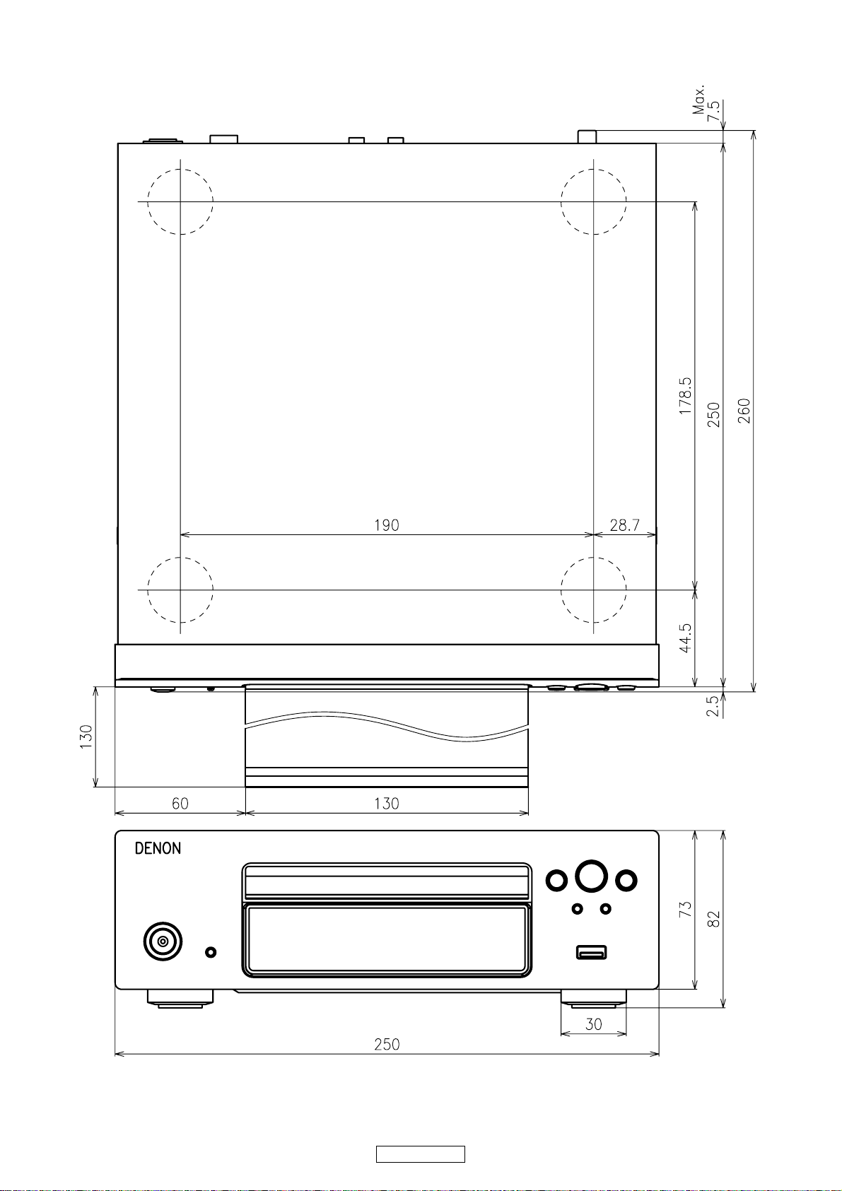
DIMENSION
3
DCD-F107
Page 4
WIRE ARRANGEMENT
If wire bundles are untied or moved to perform adjustment or parts replacement etc.,be sure to rearrange them neatly as
they were originally bundled or placed afterward.
Otherwise, incorrect arrangement can be a cause of noise generation.
Wire arrangement viewed from the top
Front Panel side
Back Panel side
4
DCD-F107
Page 5
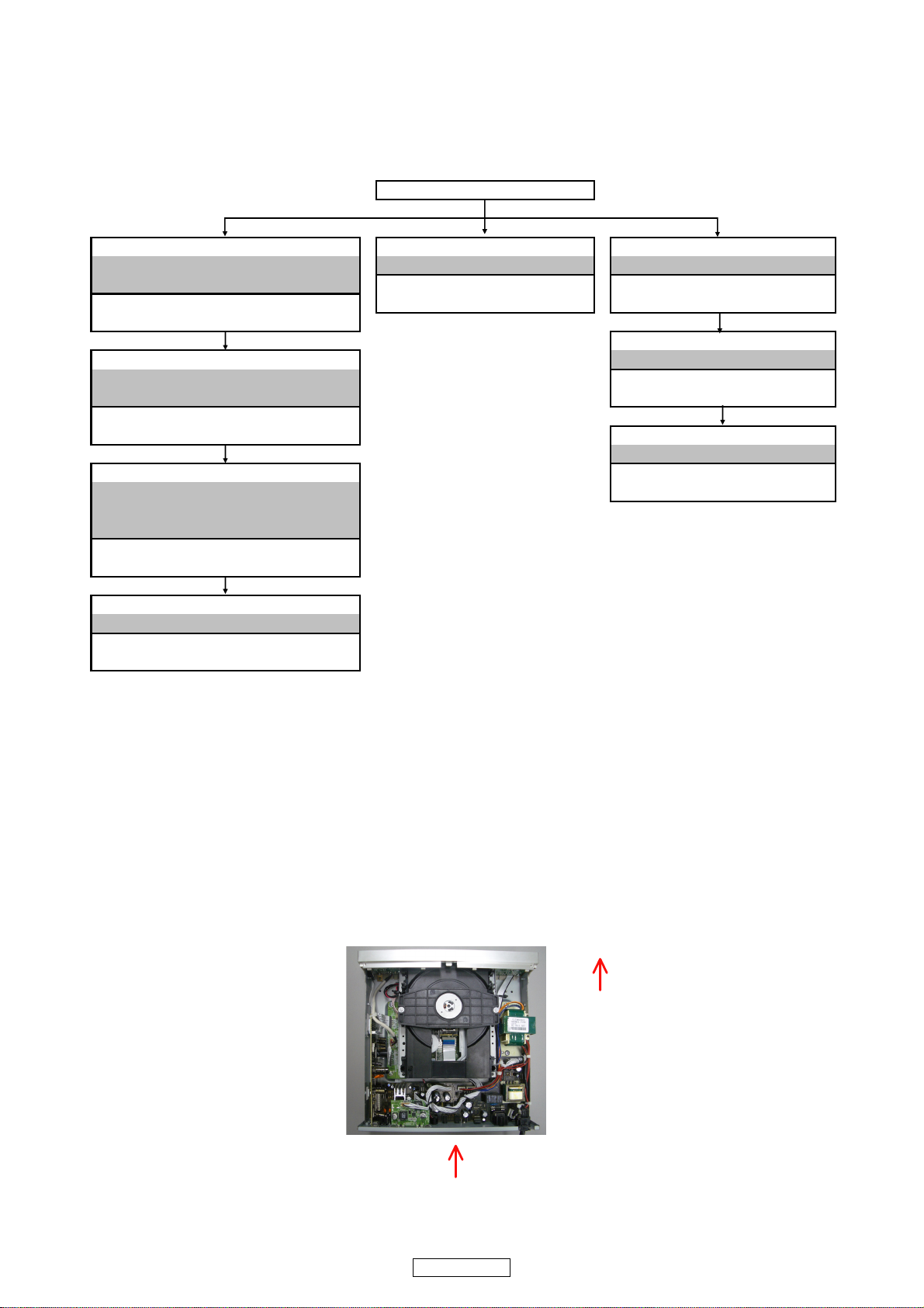
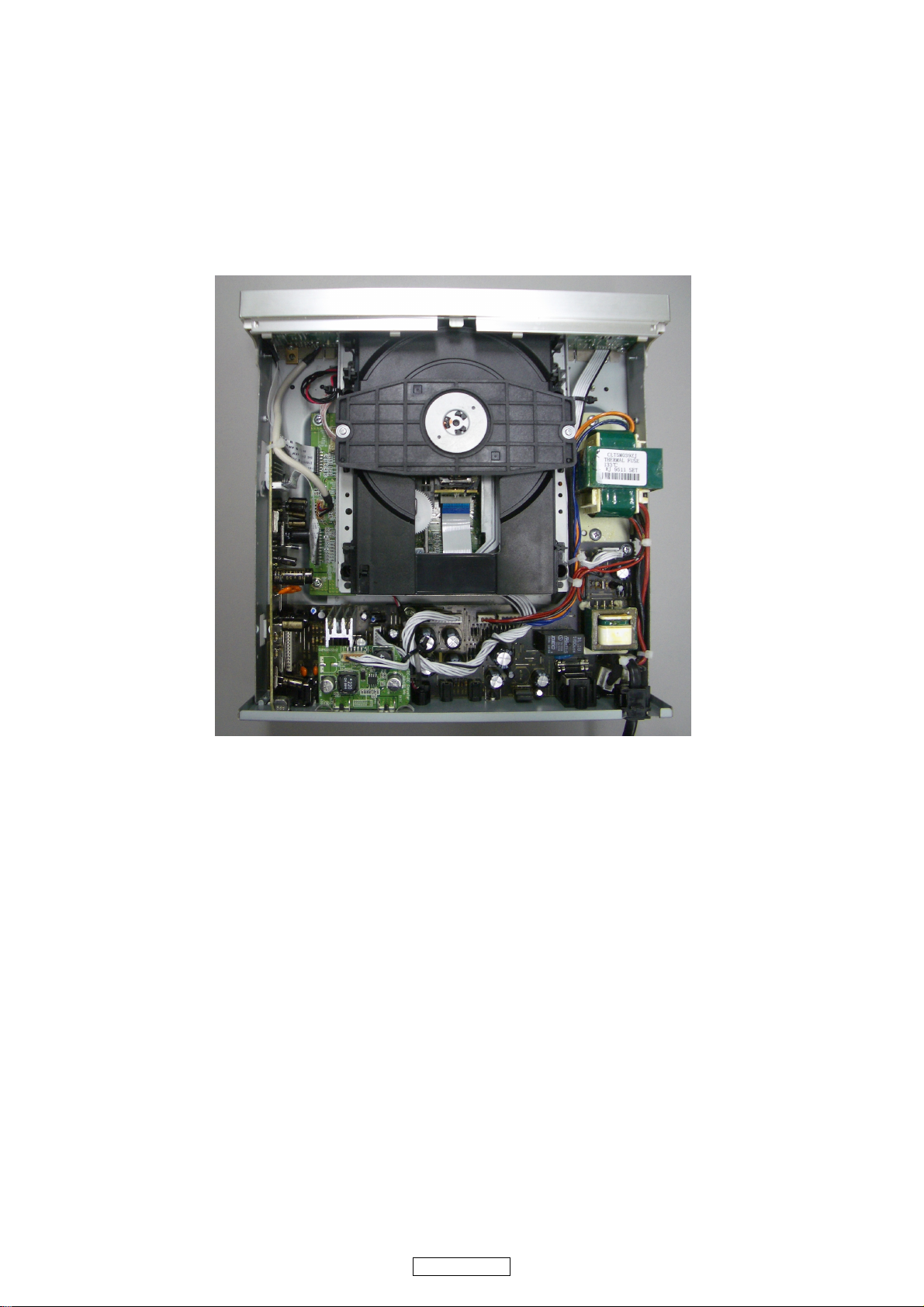
DISASSEMBLY
TOP COVER
LENAPRAERSNARTREWOPROOD
Refer to "DISASSEMBLY 1.DOOR" Refer to "EXPLODED VIEW" Refer to "EXPLODED VIEW"
Refer to "EXPLODED VIEW" LENAPRAERSNARTREWOP
)01M:WEIVDEDOLPXEfo.oN.feR()3C:WEIVDEDOLPXEfo.oN.feR(ROOD
(Ref. No. of EXPLODED VIEW : P1)
AUDIO PCB
FRONT PANEL ASSY
Refer to "EXPLODED VIEW"
Refer to "DISASSEMBLY 2.FRONT PANEL ASSY" INPUT PCB
Refer to "EXPLODED VIEW" (Ref. No. of EXPLODED VIEW : C7)
FRONT PCB
(Ref. No. of EXPLODED VIEW : C1)
POWER PCB
㩷
Refer to "EXPLODED VIEW"
MECHANISM
POWER PCB
Refer to "DISASSEMBLY
㩷
(Ref. No. of EXPLODED VIEW : C6)
3.MECHANISM"
Refer to "EXPLODED VIEW"
CD MECHANISM ASSY
(Ref. No. of EXPLODED VIEW : C5)
CD MAIN PCB
Refer to "EXPLODED VIEW"
CD MAIN PCB
(Ref. No. of EXPLODED VIEW : C4)
The viewpoint of each photograph
(photography direction)
[View from above]
Front side
Direction of photograph: A
• Disassemble in order of the arrow of the figure of following flow.
• In the case of the re-assembling, assemble it in order of the reverse of the following flow.
• In the case of the re-assembling, observe "attention of assembling" it.
About the photos used for descriptions in the “DISASSEMBLY” section.
• The direction from which the photographs used herein were photographed is indicated at "Direction of photograph: ***" at
the left of the respective photographs.
• Refer to the table below for a description of the direction in which the photos were taken.
• Photographs for which no direction is indicated were taken from above the product.
DCD-F107
5
Page 6
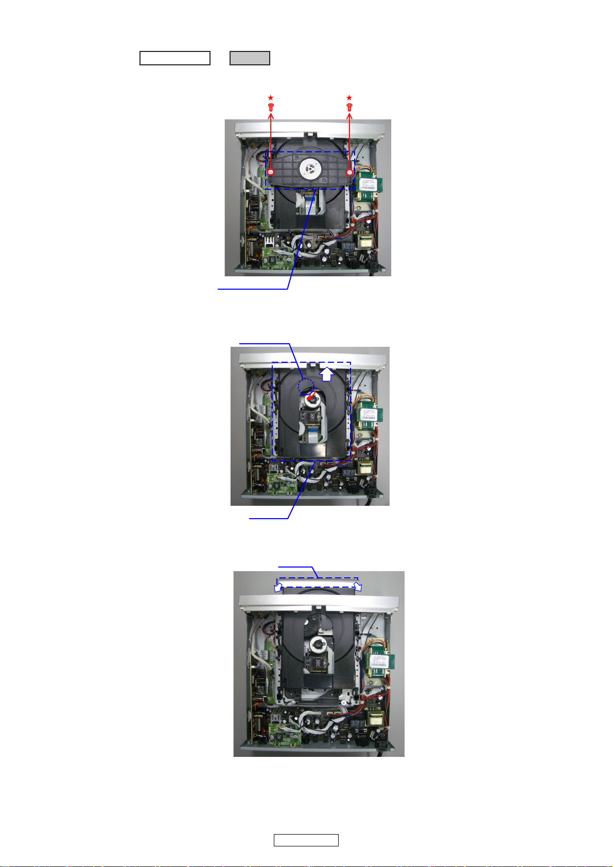
1. DOOR
TOP COVER
DOOR
→
Proceeding :
Chucking plate
Drive gear
CD tray
DOOR
(1) Take off the Chucking plate after removing screws.
(2) Open the CD tray by turning the Drive gear clockwise.
(3) Detach the DOOR.
6
DCD-F107
Page 7
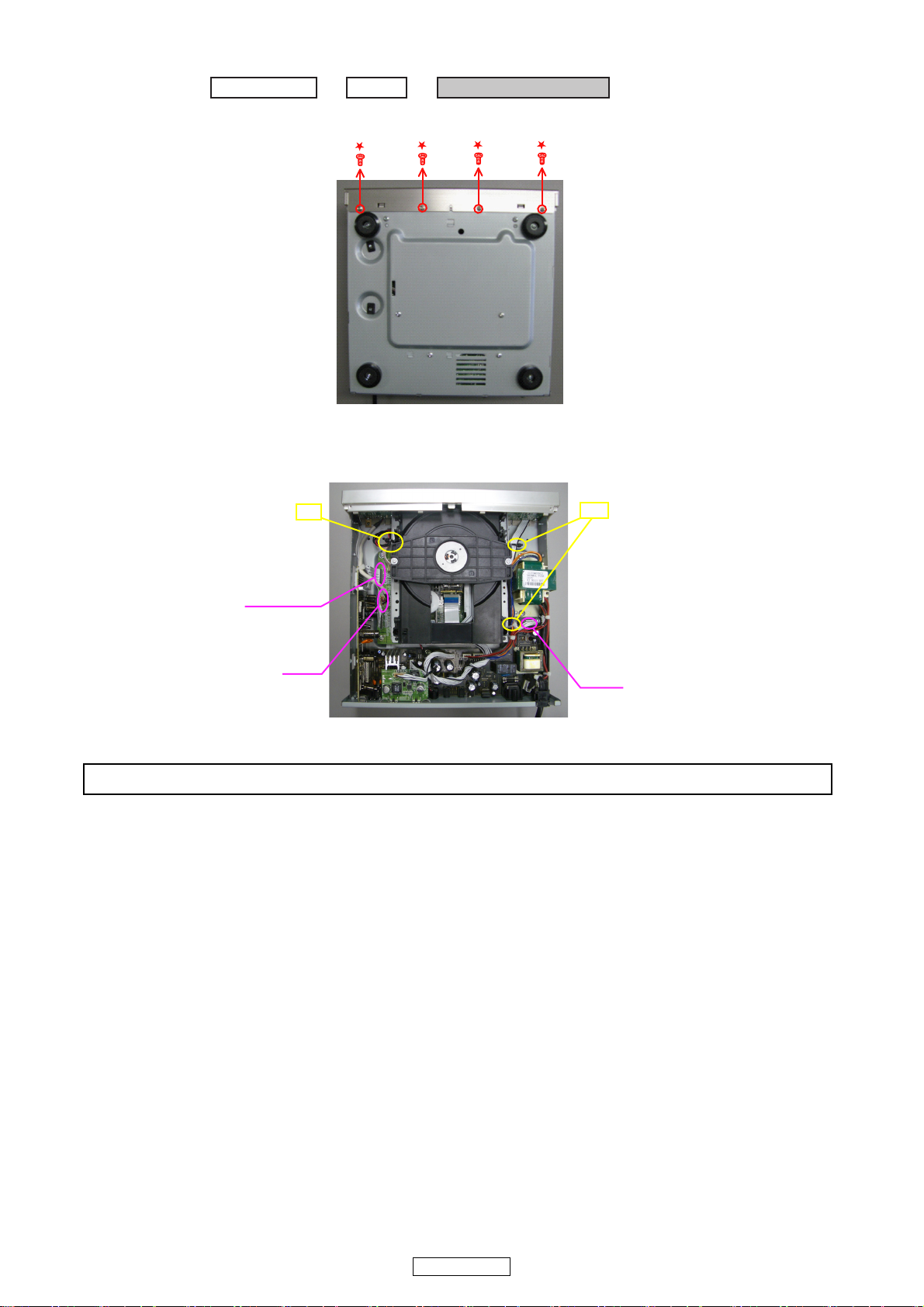
2. FRONT PANEL ASSY
TOP COVER
DOOR
→
FRONT PANEL ASSY
→
Proceeding :
View from bottom
CN97
cut
FFC Cable
CN52
cut
Please refer to "EXPLODED VIEW" for the disassembly method of each PCB included in FRONT PANEL ASSY.
(1) Remove the screws.
(2) Cut the clamp bands, disconnect the connector wires and FFC Cable.
7
DCD-F107
Page 8
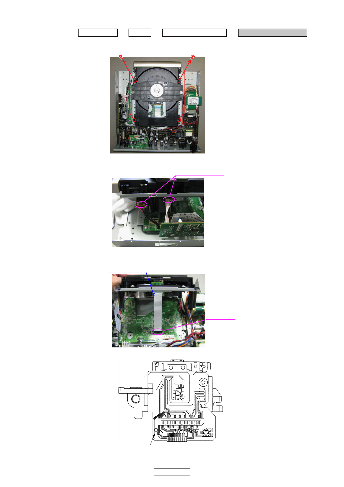
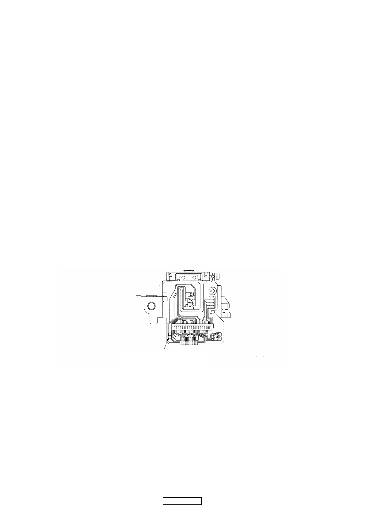
3. CD MECHANISM ASSY
Proceeding : CD MECHANISM ASSY
→
TOP COVER
DOOR
→
FRONT PANEL ASSY
→
ً
ً
Direction of photograph: A
Connector wires
Soldering place
Direction of photograph: A
FFC Cable
Laser short-circuit
(1) Cut the clamp bands, disconnect the connector wires. Remove the screws.
(2) Disconnect the connector wires.
(3) Laser short-circuit in Pick-up of CD MECHANISM, then disconnect the FFC Cable.
8
DCD-F107
Page 9
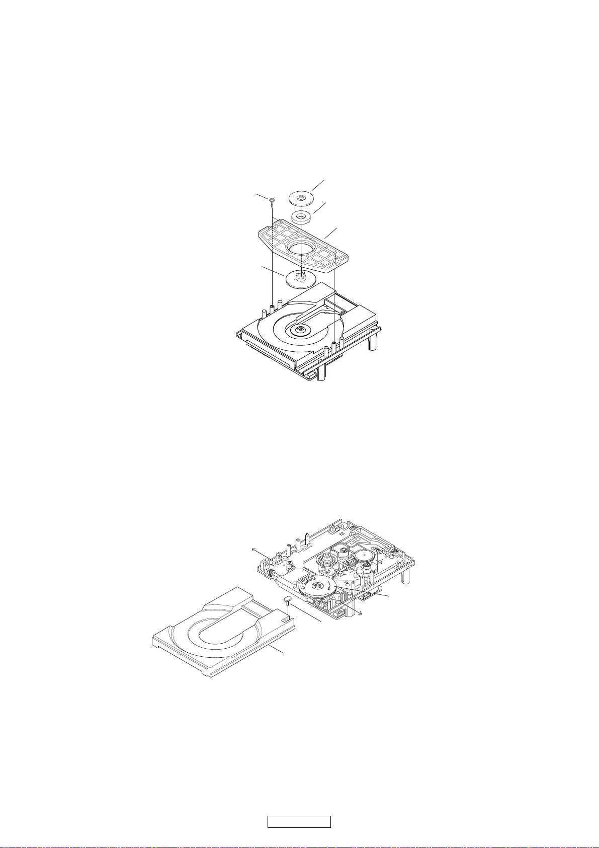
DISASSEMBLY OF MECHANIC
Chucking yoke
Chucking plate
Chucking pulley
Screws
Mugnet
(Follow the procedure below in reverse order when reassembling.)
Caution : The optical pickup can damaged by sassily by static electricity charged on human body. Take necessary anti-static
measures when repairing around the optical pickup.
1. Chucking plate
(1) Remove 2 top screws, then detach the Chucking plate.
(2) Detaching the Chucking pulley and chucking yoke by removing the 3 hooks, when abandoning CD MECHA ass’y.
2. CD tray
When abandoning CD MECHA ass’y, please detach the CD tray.
(1) Detach the Sw pin on the CD tray.
(2) Open the CD tray by turning the Drive gear clockwise.
(3) Open the Stopper as shown in the fig., then detach CD tray.
Stopper
CD tray
Drive gear
Stopper
Sw pin
9
DCD-F107
Page 10
Note Handling and Replacement of the Laser pick-up
1. Protection of the LD
Short a part of the LD circuit by soldering. After connection to a circuit, remove the short solder.
2. Precautions when handling the laser CD mechanism
• Handle the laser pick-up so that it is not exposed to dust.
• Do not leave the laser pick-up bare. Be sure to cover it.
• If dust adheres on lens of the pick-up, blow it off with a blower brush.
• Do not shock the laser pick-up.
• Do not watch the light of the laser pick-up.
3. Cautions on assembling and adjustment
• Be sure that to the bench, jig, head of soldering iron (with ceramic) and measuring instruments are well grounded.
• Workers who handle the laser pick-up must be grounded.
• The finished mechanism (prior to anchoring in the set) should be protected against static electricity and dust. The mechanism must be stored that damaging outside forces are not received.
• When carrying the finished mechanism, hold it by the
chassis body
• For proper operation, storage and operating environment should not contain corrosive gases. For example H
CI2 etc. In addition storage environment should not have materials that emit corrosive gases especially from silicic, cyanic,
formalin and phenol group. I the mechanism or the set, existence of corrosive gases may cause no rotation in motor.
2S, SO2, NO2,
4. Determining whether the laser pick-up is defective
•
Measure the waveform at RFO-VC on "MCU PCB Unit ".
( For measuring points and waveforms, see pages 26, 27.)
• The laser pick-up is OK if the amplitude level of the measured RFO waveform is between 0.4 and 1.1 Vp-p, defective otherwise.
Protective soldering place for laser diode.
10
DCD-F107
Page 11
Diagnostics of optical pickup and replacing traverse unit d
S
/C: XXXmA/YYYmA
L
ASER CURRENT
Disc no read, unsteady playback, etc.
Laser drive current (Iop) check
Present value exceeds the initial value by 1.5 times
Traverse Unit replacing
Laser current (Iop) memorizing after replacement
Make failure diagnostics of the Optical Pickup as follows.
If the laser drive current (Iop) becomes more than 1.5 times of the initial value, the Optical Pickup should be replaced.
The laser drive current initial value is checked by "Iop checked Method" of next page.
In case of replacing the Pickup, change the whole part of the Traverse Unit.
No mechanical adjustment is necessary after the replacement.
Laser drive current initial value:
・13 flashing
XXX : Initial value : Stored data (EEPROM stored value)
YYY : Current value
11
DCD-F107
Page 12
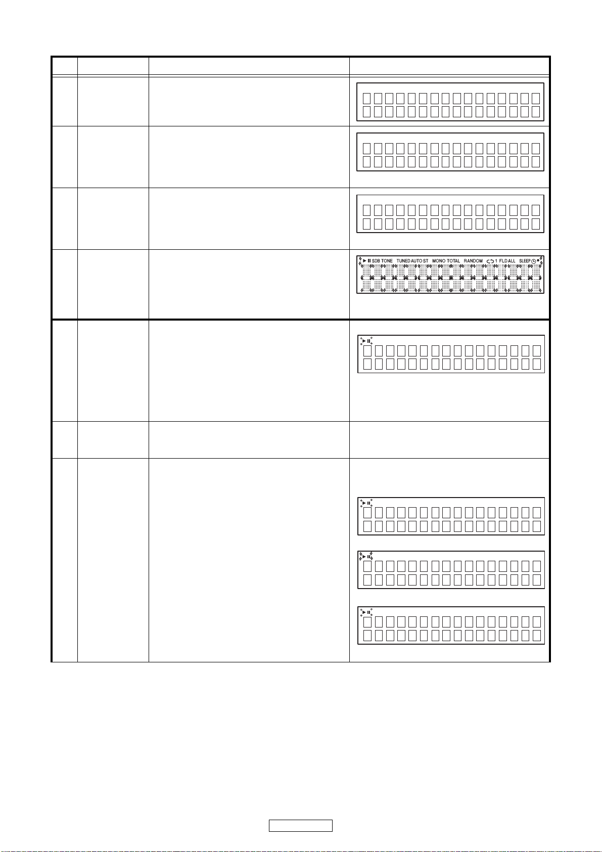
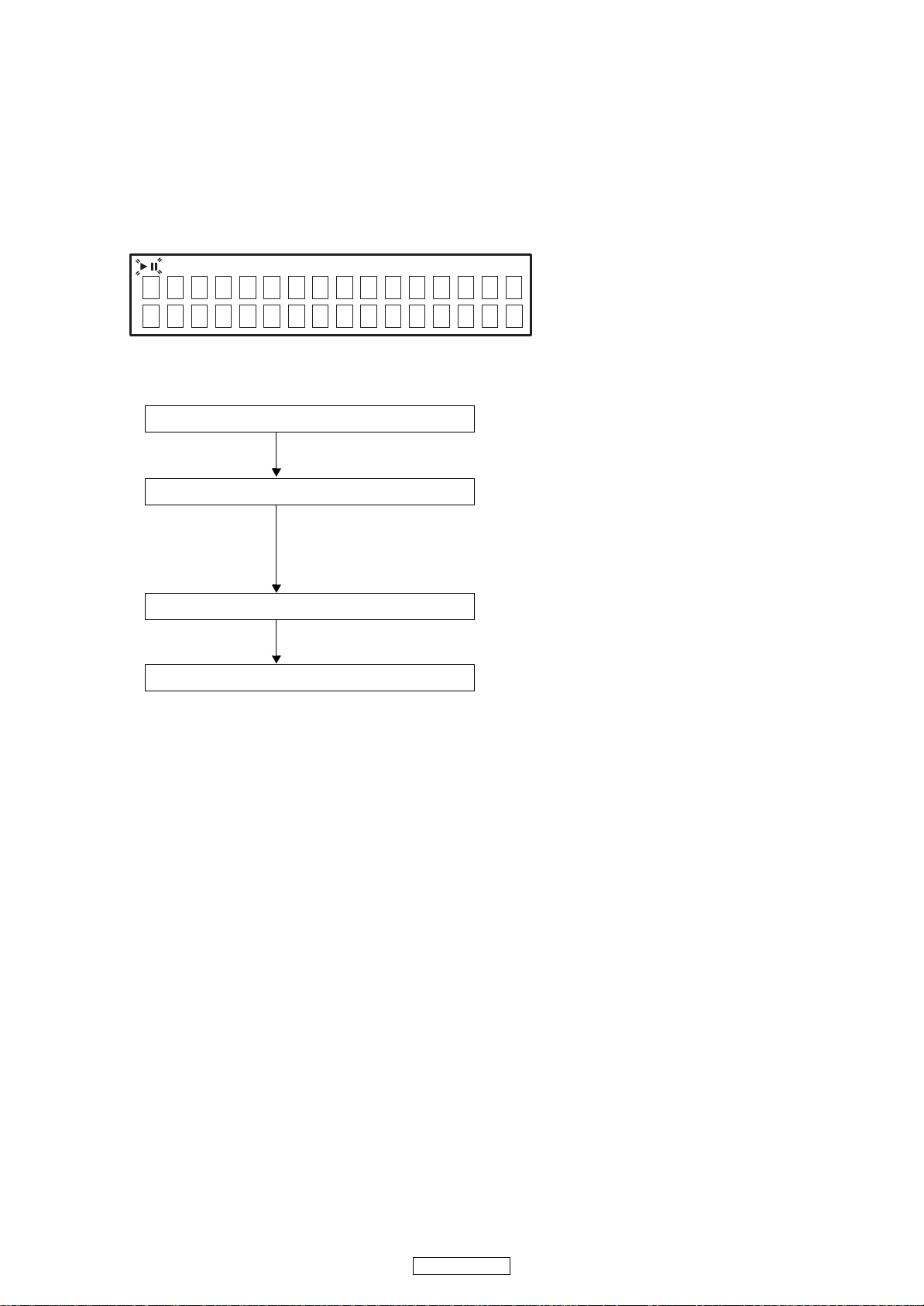
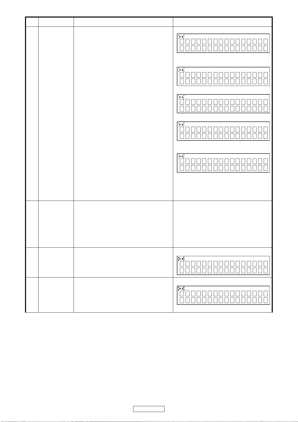
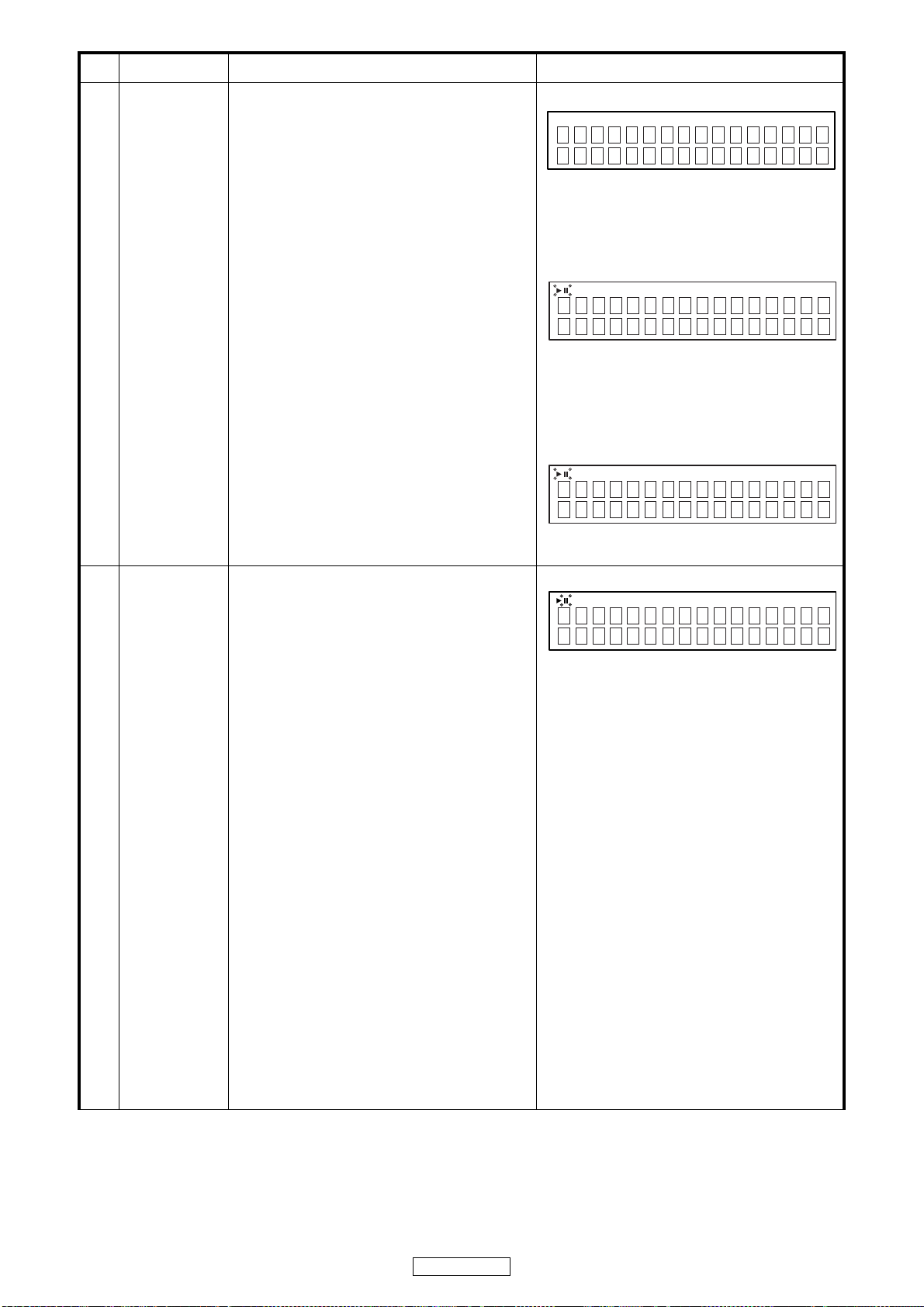
SPECIAL MODE
No Key name Function Display
• AC is turned on while pressing the 5 and 2 button
1
Service mode
same time on DCD-F107.(Model name display)
DCD-F107
Version No. of
1.1
main μ-com
Display mode
Version No. of
1.2
USB μ-com
Display mode
1.3 FLD check mode
2 CD test mode
2.1 Disc loading
• Press the 9 button.
• Press the 9 button while version No. of main
μ-com is displayed.
• When display is version No. of USB μ-com and
the 9 button is pressed, turn on the entire display is flashing with an interval of about 1 second.
• Press the 9 button again in the turn on each
grid of FLD. (Each grid is displayed at interval of 1
second.)
• AC is turned on while pressing the 5 and 2 button
same time on DCD-F107.(Entering the Service
mode)
• Press the 2 and
version display, FLD check mode and heat runmode.(CD TEST MODE display)
• Press the DISC/USB button continuously for over
3 seconds to display the version number of main
μ-com.
• Press the 5 button to open the tray.
• Set a disc on the tray, then press the 5 button
again to close the tray.
• Press the
steps.
q LD ON (with servo still stopped)
13 button. Execute the following
/
13 button same time while
/
Ver xxxx
"****" : Version number of main μ-com
USB_Ver ****
"****" : Version number of USB μ-com
13 flashing
00 CD TEST MODE
・13 flashing
q
2.2 Servo check
w FOCUS ON (disc rotation, tracking off)
If no disc loaded, retry then stop.
e CLV ON
12
DCD-F107
01 LD ON
w
02 Focus ON
e
03 CLV ON
Page 13
No
2.2 Servo check
2.3
Key name
Pickup
movement
Function Display
r TRACKING ON
t SUB CODE readout (playback sound output)
• The BER (Block Error Rate) generated in 1
second's time is displayed on the upper tier of
the display.
• The playback position (IN/MID/OUT) can be
changed by pressing the 8 or 9 button.
• The count of the errors that could not be
corrected with the C1 error correction system is
displayed.
y When display is as in t and the
pressed, conduct BER (Block Error Rate)
display for 2 seconds.
• The BER (Block Error Rate) generated in 10
second's time is displayed of the display.
bPress
second to switch directly to SUB CODE readout
in step
・In the stop mode, pickup moves in REV (inwards)
or FWD (outwards) direction when 8 or 9
button pressed.
・When 8 button pressed, move to stop
operation after detection that inner switch has
turned on.
・Pickup movement stops when button released.
(Pickup moves while button is pressed.)
/
13 button continuously for over 1
t.
/
13 button is
r
04 Tracking ON
t
[IN]
NERR######
I
05 @@
[MID]
ID ERR ######
M
05 @@
[OUT]
UT ERR ######
O
05 @@
###### : B.E.R., @@ : T.No, XX:XX : Time
y
PP ERR ######
P
Tr
Tr
Tr
XX:XX
XX:XX
XX:XX
ERR *** ***
PPP : Playback position (IN/MID/OUT)
###### : 1
Continuous display of previous time
second's B.E.R.
, *****:
10 second's B.E.R.
2.4 Stop
2.5 All servo on
・When 2 button is pressed, play operation and
servo stop.
・After stopping, conduct reading of auto adjust
values.
・When 2 and 5 button is pressed, all servos turn
on, auto adjustment is performed and switch to
playback operation. (Playback sound output)
(NOTE)When the 2 button is pressed for over 1
second while the laser turns on and the laser
current is measured.
・13 flashing
00 CD TEST MODE
・13 flashing
@@
Tr
@@ : T.No, XX:XX : Time
XX:XX
13
DCD-F107
Page 14
No
Key name
Function Display
Laser current is
2.6
display
・When the 2 button is pressed for over 1 second
while the DCD-F107 is in the stop mode, the
laser turns on and the laser current is measured.
・The laser drive current undergoes A/D
conversion for calculation. Decimal values are
discarded.
・The first current value is measured 3 seconds
after the laser turns on.
・The current value is updated every 3 seconds.
・Press the 2 button, CD test mode display (2)
reappears.
・Stored data is not cleared, even when the DCD-
F107 is reset.
q Overwriting the stored data
・When the
seconds while the laser current is displayed, the
current value is stored in the EEPROM
(overwriting the stored data).
・Once rewriting is completed, the display in 2.6
reappears.
・Rewriting is performed upon shipment from the
factory and when the mechanism is replaced.
・Press the 2 button after executing the servo auto
adjustment.
・When 9 button is pressed, the adjustment
values are displayed in the following order.
q FOCUS BALANCE
w FOCUS GAIN
/
13 button is pressed for over 5
・ 13 flashing
/C: XXXmA/YYYmA
S
ASER CURRENT
L
XX : Stored data : EEPROM Stored value
YY : Current value
q
TORED
S
ASER CURRENT
L
・13 flashing
q
X
X
OCUS BALANCE
F
XX : Adjustment value
w
Adjustment value
2.7
display
e TRACKING BALANCE
r TRACKING GAIN
tFOCUS OFFSET
y TRACKING OFFSET
X
X
OCUS GAIN
F
XX : Adjustment value
e
X
X
RACKING BALANCE
T
XX : Adjustment value
r
X
X
RACKING GAIN
T
XX : Adjustment value
t
X
X
OCUS OFFSET
F
XX : Adjustment value
y
X
X
RACKING OFFSET
T
XX : Adjustment value
14
DCD-F107
Page 15
No
Key name
Function Display
Adjustment value
2.7
display
Accumulated
2.8
laser on time
display
u RFRP
i Return to q.
(Note)If auto adjustment is not completed, proper
values are not displayed.
・When the DISC/USB and 5 button is pressed
while the DCD-F107 is in the stop mode, the
accumulated laser on time is displayed.
・The laser drive times are added and the result is
displayed.
・One count corresponds to 10 minutes. (Values
under 10 minutes are discarded.)
・Count values are stored in the EEPROM every 10
minutes.
・The accumulated laser on time is displayed in
hours.
・Laser ON/OFF is monitored and counted.
・Press the 2 button, CD test mode display (2)
reappears.
・The count values are not cleared, even when the
set is reset.
・Minimum display specification
• No. digits stored in EPROM: 4, 0xFFFF
• No. digits displayed: 5
• When the time exceeds 10922 hours, the
stored data is not updated and the value is
fixed to 0xFFFF.
(The display is fixed to 10922 hours.)
u
X
X
FRP
R
XX : Adjustment value
・13 flashing
XXXX hour
X
ASER ON TIME
L
3
CD heat run
mode
q Count value is reset
・When the
seconds while the accumulated laser on time is
displayed, the count value is reset.
・After resetting is completed, the display in 2.6
(00000 hours on the top line) reappears.
・Count value is reset upon shipment from the
factory and when the mechanism is replaced.
・AC is turned on while pressing the 5 and 2 button
same time on DCD-F107.
・Switches to mode according to button input.
・Press the reverse button to switch the mode while
displaying the version of the main μcom.
(Normal heat run mode, Heat run short mode,
Automatic mounting mode.) d
・If an error occurs, display the error and stop
operation at that point.
・Number of operations held.
・While heat run, the operation of each button is not
valid except the ON/STANDBY button and
pressing the 5 and 2 button same time.
/
13 button is pressed for over 5
q
LEAR
C
ASER ON TIME
L
15
DCD-F107
Page 16
No
Key name
Function Display
Normal heat run
3.1
mode
・Press the
displayed or H.R.NORMAL is displayed.
・Count this as the 0th heat run repetition.
q Play from the first to last track on disc.
w After disc playback has finished, move pickup
to innermost position and open tray.
e When loader open status detected, close tray
again, re-read TOC and start playback from the
first track on the disc.
r The heat run repetition no. is incremented
(increased by 1) when the tray is opened.
※ If the 2 and 5 button is pressed while operat-
/
13 button while name of the model is
ing, number of heat run is displayed for 3 seconds.
・Model Name display
・H.R.NORMAL display
.R.NORMAL
H
・Normal heat run mode
Normal display except when 1 light, 3 flashing
q Normal display except when 1 light, 3 flashing
w
CD XXXX
XXXX : No. of heat run repetitions
e Normal display except when 1 light, 3 flashing
r
CD XXXX
XXXX : No. of heat run repetitions
Heat run Short
3.2
mode
t Conduct q to e repeatedly.
/
・Press the
H.R.SHORT is displayed.
・Count this as the 0th heat run repetition.
q Play the last track only on disc.
w After disc playback has finished, move pickup
to innermost position and open tray.
e When loader open status detected, close tray
again, re-read TOC and start playback from the
first track on the disc.
r The heat run repetition no. is incremented
(increased by 1) when the tray is opened.
※ If the 2 and 5 button is pressed while oper-
13 button while name of the
ating, number of heat run is displayed for 3
seconds.
・H.R.SHORT display
.R.SHORT
H
・Heat run Short mode
Normal display except when 1 light, 3 light
q Normal display except when 1 light, 3 light
w
CD XXXX
XXXX : No. of heat run repetitions
e Normal display except when 1 light, 3 light
r
CD XXXX
XXXX : No. of heat run repetitions
t Conduct q to e repeatedly.
16
DCD-F107
Page 17
No
Key name
Function Display
Automatic
3.3
mounting mode
3.4 Error display
・Press the
H.R.CHACKING is displayed.
・Count this as the 0th heat run repetition.
q Play the last track only on disc.
w The heat run repetition no. is incremented
(increased by 1) when the tray is opened.
※ If the 2 and 5 button is pressed while oper-
ating, number of heat run is displayed for 3
seconds.
e Conduct q repeatedly.
E1-00 : Disc cannot be detected
E1-01 : Tracking offset adjustment not possible
E1-02 : Focus offset adjustment not possible
E2-00 : Focus servo dropped during playback.
E2-01 : Focus servo dropped during searching.
E2-03 : Focus servo dropped during TOC reading.
E2-05 : Focus servo dropped during manual
E2-10 : Subcode can no longer be read during
E2-11 : Subcode can no longer be read during
E2-12 : Subcode can no longer be read during
E2-14 : Subcode cannot be read during pause
E2-15 : Subcode cannot be read during manual
E3-00 : TOC could not be read within specified
E3-01 : PVD/SVD analysis could not be
E4-04 : Search time out
E4-05 : Error in communications with CD decoder
E5-00 : Inner switch not on
E6-00 : Inner switch not off
E8-00 : Tray is not opened by the specified time.
E8-01 : Tray is not closed by the specified time.
E9-01 : Other error
/
13 button while name of the
search.
playback
searching
TOC reading
search
time
completed within specified time
・H.R.CHACKING display
.R.CHACKING
H
・Heat run short mode
Normal display except when 1 flashing, 3 flashing
qNumber of heat run is display
CD XXXX
XXXX : No. of heat run repetitions
・READING, CLOSEdisplay
Normal display except when 1 flashing, 3 flashing
wNumber of heat run is display
CD XXXX
XXXX : No. of heat run repetitions
,
・
13 with mode light or flashing
CD EX-XX
X-XX : Error cord
17
DCD-F107
Page 18
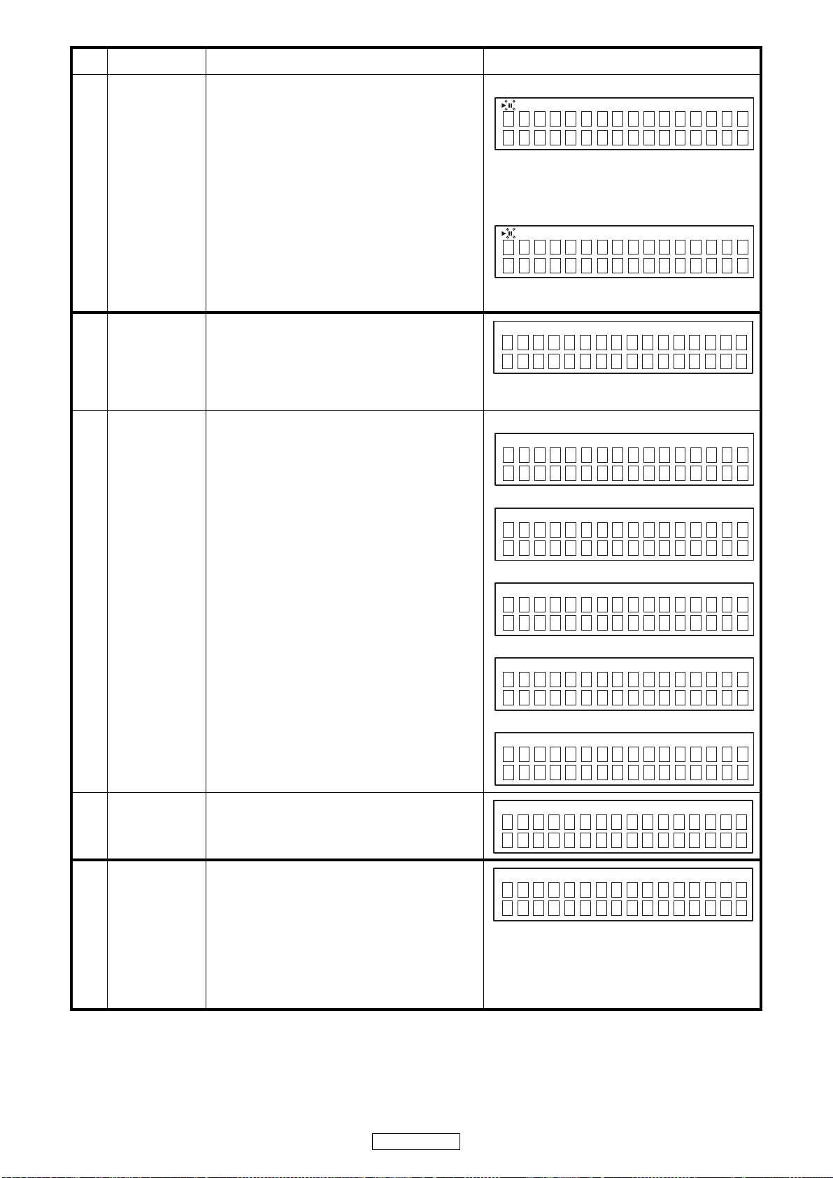
No
Key name
Function Display
3.4 Error display
Main μ-com
4
Version up
mode
q Number of heat run is display
・Press the 9 button while the error is displayed.
・ No. heat runs is displayed for 5 seconds, the error
display reappears.
w The track no. and time when the error occurred is
displayed
・Press the 8 button while the error is displayed.
・ The track no. and time when the error occurred is
displayed for 5 seconds, then error display
reappears.
・AC is turned on while pressing the 5 and 2 button
same time on DCD-F107.(Entering the Service
mode)
・ While displaying model name, when 2 and the
ON/STANDBY button are pressed simultaneously,
the tray opens.
• If an the 5 or
closed, a disc will be loaded and Version up will be
started.
• " FileError" is displayed when not found upgrade
file and the tray is opened.
/
13 button is pushed and a tray is
,
q
13 with mode light or flashing
CD XXXX
XXXX : No. of heat run repetitions
・Error display reappears after 5 seconds. See 3.4.
,
13 with mode light or flashing.
w
CD 01
・Error display reappears after 5 seconds. See 3.4.
YSTEM VUP ALL
S
etDisc -> Close
S
q During a file search
YSTEM VUP ALL
S
ileSearch
F
w During a file check
Tr
01:47
4.1 Start version up
4.2 End version up
Cold start
5
(Initialize)
・After Version UP is completed, a tray is opened
and it stops in
・AC is turned on while pressing the 5 and 9
button same time on DCD-F107.
・The system is reset, and once this is completed
the unit is set to the normal mode.
DIMMER : 100%
DISC/USB : DISC
REMOTE/BROWSE : REMOTE
・The laser current initial value and laser
accumulated on time is not cleared.
YSTEM VUP ALL
S
ileCheck
F
e During deletion
YSTEM VUP ALL
S
rasig
E
r Writing
YSTEM VUP ALL
S
riting
W
t When a file is not found
YSTEM VUP ALL
S
ileError
F
YSTEM VUP ALL
S
omplete
C
INITIALIZE
18
DCD-F107
Page 19
No
6
Key name
USBμ-com
Version up
mode
Function Display
・AC is turned on while pressing the 5 and 2 button
same time on DCD-F107.(Entering the Service
mode)
・ While displaying model name, when 9 and the
ON/STANDBY button are pressed simultaneously,
the tray opens.
• If an the 5 or
closed, a disc will be loaded and Version up will
be started.
• "FileError" is displayed when not found upgrade
file and the tray is opened.
/
13 button is pushed and a tray is
OLERO VUP
B
etDisc -> Close
S
q During a file search
YSTEM VUP ALL
S
ileSearch
F
w During a file check
YSTEM VUP ALL
S
ileCheck
F
e During deletion
6.1 Start version up
6.2 End version up
EEPROM TEST
7
mode
・After Version UP is completed, a tray is opened
and it stops in
・Press POWER SW while simultaneously pressing
ON/STANDBY and DISC/US button.
・POWER LED lights to the orange (TEST start).
・After EEPROM TEST, in the case of OK, LED
lights to the green.
・After EEPROM TEST, in the case of NG, LED
lights to the red.
・Mode is cancelled with POWER OFF.
YSTEM VUP ALL
S
rasig
E
r Writing
YSTEM VUP ALL
S
riting
W
t When a file is not found
YSTEM VUP ALL
S
ileError
F
OLERO VUP
B
omplete
C
19
DCD-F107
Page 20
Special mode transition diagram
Start
Ver UP
5
1/3 or
USB Ver UP mode
“Ver UP USB” display
9 +
ON/STANDBY
Start
Ver UP
5
1/3 or
Main Ver UP mode
“Ver UP Main” display
+
ON/STANDBY
2
8
9
Ver.display
USB μ-com
2+1/3
8
9
2+1/3
FL all light
The entire display is
flashing with an interval
of about 1 second.
9
8
5+2+AC_ONService mode
Model Name display
1/3
8 or 9
“DCD-F107”
Main μ-com
Ver.display
9
8
H.R.NORMAL display
1/3
2+1/3
8
9
2+1/3
9
CD test mode
FL tube
The display for each grid.
(It displays at intervals
of 1 second.)
Main Ver. display reappears.
2+1/3
2+1/3
2+1/3
8
8
H.R.SHORT display
9
1/3
H.R.CHACKING display
1/3
H.R.NORMAL operation
TOC read → playback
title-all of the disc. →
OPEN → CLOSE →
TOC read
It displays repeatedly.
DCD-F107
H.R.SHORT operation
20
TOC read → playback
title-end of the disc. →
OPEN → CLOSE →
TOC read
It displays repeatedly.
H.R.CHACKING operation
TOC read → OPEN →
CLOSE → TOC read
It displays repeatedly.
Page 21
TROUBLE SHOOTING
FLOW CHART NO.1
The power cannot be turned on.
㸣
Is Power LED lit? 㸢No
㸣Yes
Is the +3.3V_NSW line voltage normal? 㸢No
㸣Yes
Is the +5_SYS line voltage normal? 㸢No
㸣Yes
Is the "H" level MCU Reset to Pin(77) of IC11? 㸢No
㸣Yes
Is normal state restored when once unplugged power
cord is plugged again after several seconds?
㸣Yes
Check each voltage regulator circuit and service it if defective.
㸢No
FLOW CHART NO.2
+3.3V_D is not outputted.
㸣
Is +7V_DRV voltage supplied to Pin(1) of IC93? 㸢No
Check if there is any leak or short-circuiting rectifier circuit
of SUB Power transformer, and service it if defective.
(T901,IC94,IC95,Q905-Q909,D930,D931,D934-D936)
Check IC11,IC12and the periphery circuit, and service it if
defective.
Check if there is any leak or short-circuiting rectifier circuit
of Power transformer, and service it if defective.
(Main Trans,IC81,D917-D923)
㸣Yes
Check IC93 and the periphery circuit, and service it if
defective.
FLOW CHART NO.3
The fluorescent display tube does not light up.
㸣
Is +3.3V_D. voltage supplied to Pins(37) of F701? 㸢No Check the +3.3V_D line and service it if defective.
㸣Yes
Is the voltage of approximately +42V supplied to
Pin(38) of F701?
㸣Yes
Is the voltage of approximately +7V supplied to
Pin(1),(43) of F701?
㸣Yes
Check the fluorescent display tube control signal of a
microcomputer. (FL_RST,FL_CS,FL_CLK,FL_MDT)
㸢No
㸢No Check the FL1/FL2 line and service it if defective.
Check D924-927,Q904 and periphery circuit, and service
it if defective.
21
DCD-F107
Page 22
FLOW CHART NO.4
The key operation is not functioning.
㸣
Are the contact point and the installation state of the
key switches (S701-S704,S706-S708) normal?
㸣Yes
When pressing each switches (S701-S704,S706S708), do the voltage of Pin (4),(5),(6),(99),(100) of
IC11 decrease?
㸣Yes
Replace IC11.
㸢No
㸢No
FLOW CHART NO.5
No operation is possible from the remote control unit.
㸣
Are the System Connector (DENON BUS) Cables
nomal?
㸣Yes
Is +5V_SYS voltage supplied to Pin(8) of IC96? 㸢No
㸣Yes
Re-install the switches (S701-S704,S706-S708) correctly
or replace the poor switch.
Check the switches (S701-S704,S706-S708) and their
periphery, and service it if detective.
Check IC94 and the periphery circuit, and service it if
defective.
Check Control Signal Pin(2) DBTXD,Pin(3) DBRXD of
JK93,JK94
㸣Yes
Refer to DRA-F107 TROUBLESHOOTING_Remote Control
㸢No
FLOW CHART NO.6
The disc tray cannot be opened and closed.
㸣
Is the normal control voltage inputted to Pin(6) of
IC11? Refer to "FLOW CHART NO.4" <The key
operation is not functioning.>
㸣Yes
Check the line between CN23 and IC14, and service it if
defective.
㸢No Replace the "OP/CL" button (S706).
Check IC96,IC11 and the periphery circuit, and service it
if defective.
22
DCD-F107
Page 23

FLOW CHART NO.7
Audio is not outputted normally.
㸣
Set the disc on the disc tray, and playback.
㸣
Are the analog audio signals outputted to Pin(1),(7) of
IC41,IC42
IC41Pin(1),(7) : AUDIO (L-),(L+)
IC42Pin(1),(7) : AUDIO (R-),(R+)
㸣Yes 㸣Yes
Is the "H" level MUTE line to Pin(21) of CY11? Is the "H" level Reset Signal for DAC to Pin(14) of IC31?
㸣Yes 㸣Yes
Check A_MUTE line and service it if defective.
IC44 Pin(25) A_MUTE H : mute / L : play 㸣Yes
㸢No
Check AUDIO+V(+6V) and AUDIO-V(-6V) line and
service it if defective.
Check the DAC(IC31) digital audio data signal from a
DSP (IC17). (BCK,LRCK,DATA_S1L,DATA_S1R)
Check the DAC(IC31) control signal from a
microcomputer (IC11). (DAC_CS,DAC_MCK,DAC_MDT)
㸣Yes
Check DAC(IC31)_Vcc(+3.3V_D2) line and service it if
defective.
㸣Yes
Replace IC31.
FLOW CHART NO.8
DIGITAL OUT(OPTICAL) Audio is not outputted normally.
㸣
Is +5VA voltage supplied to Pin(2) of JK91? 㸢No
㸣Yes
Check Data Signal Pin(3) D_OUT of JK91. 㸢No
Check IC71 and the periphery circuit, and service it if
defective.
Check Pin(33) DOUT of IC17 and the periphery circuit,
and service it if defective.
23
DCD-F107
Page 24

FLOW CHART NO.9
USB PLAY don't work normally.
㸣
Is VBUS(+5V) voltage supplied to Pin(1) of JK71? 㸢No
㸣Yes
Check Data Signal from USB UNIT.
JK71 2,3pin䇭䇭+D,-D
㸢No
FLOW CHART NO.10
CD PLAY don't work normally.
㸣
Is +7V_DRV voltage supplied to Pin(21),(22) of IC14? 㸢No
㸣Yes
Is +3.3V_D voltage supplied to Pin(3) of IC20? 㸢No
㸣Yes
Is the "H" level CD Reset to Pin(69) of IC17? 㸢No
㸣Yes
Is the "H" level CD Reset to Pin(1) of IC15? 㸢No
㸣Yes
Check IC71 and the periphery circuit, and service it if
defective.
Check IC15 and the periphery circuit, and service it if
defective.
Check if there is any leak or short-circuiting rectifier circuit
of Power transformer, and service it if defective.
(Main Trans,IC81,D917-D923)
Check IC93,D917,D918 and the periphery circuit, and
service it if defective.
Check IC11,IC15 and the periphery circuit, and service it
if defective.
Pin(57) RST1,Pin(26) USB_RST of IC11OK?
Pin(68) RST2 of IC15 OK?
Check CD Controle wave and service it if defective.
RFEQO,RFO,FSMONIT,FOO,TEI,TRO,FMO,DMO of
IC17
24
DCD-F107
Page 25

MEASURING POINT AND WAVEFORMS
MEASURING POINT
CUP12202 MAIN PCB ASSY (Component side)
o OPSW
Q0 CLSW
u FMO
i DMO
r FOO
w RFOq RFEQO
y TRO
Q2 LOAD-
Q1 LOAD+
CUP12202 MAIN PCB ASSY (Foil side)
e FSMONIT
(IC17 : 21pin)
t TEI
(IC17 : 24pin)
25
DCD-F107
Page 26

WAVEFORMS
y
y
㧕
y
T
①RFEQO
㽲RFEQO
1. DISC PLAY RF WAVEFORM㧔EYE-PATTERN
1.1 CD㧔TCD-784㧕Pla
③FSMONIT
1.2 CD-R㧔TCD-R000RM㧕Pla
③FSMONIT
②RFO
④FOO
⑤TEI
⑥ TRO
⑦FMO
⑧DMO
②RFO
④FOO
⑤TEI
⑥ TRO
⑦FMO
⑧DMO
2. DISC DETECTION
2.1 CD㧔TCD-784㧕DISC DETECTION
1V
200mV
2V
500Mv
2V
1V
2V
2.2 CD-R䋨TCD-R000RM䋩DISC DETEC
1V
200mV
2V
500Mv
2V
1V
2V
㽲RFEQO
1.3 CD-RW䋨TCD-W000RM 䋩Pla
②RFO
③FSMONIT
④FOO
⑤TEI
⑥ TRO
⑦FMO
⑧DMO
2.3 CD-RW䋨TCD-W000RM䋩DISC DETECTION
1V
200mV
2V
500Mv
2V
1V
2V
26
DCD-F107
Page 27

3. TOC READ
3.1 CD㧔TCD-784㧕TOC READ
4. FOCUS ADJUSTMENT
4.1 CD㧔TCD-784㧕FOCUS ADJUSTMENT
②RFO
③FSMONIT
④FOO
⑤TEI
⑥ TRO
⑦FMO
⑧DMO
②RFO
③FSMONIT
④FOO
⑤TEI
⑥ TRO
⑦FMO
⑧DMO
1V
200mV
2V
500Mv
2V
1V
2V
3.2 CD-R䋨TCD-R000RM䋩TOC READ 4.2 CD-R䋨TCD-R000RM䋩FOCUS ADJUSTMENT
¬
1V
200mV
2V
500Mv
2V
1V
2V
3.3 CD-RW㧔TCD-W000RM 㧕TOC READ 4.3 CD-R䋨TCD-R000RM䋩FOCUS ADJUSTMENT
②RFO
③FSMONIT
④FOO
⑤TEI
⑥ TRO
⑦FMO
⑧DMO
⑨OPSW
⑩CLSW
⑪LOAD+
5. LOADER OPEN-CLOSE
OPEN
CLOSE
¬1V
200mV
2V
500Mv
2V
1V
2V
5V
5V
5V
⑫LOAD-
5V
27
DCD-F107
Page 28

SEMICONDUCTORS
Only major semiconductors are shown, general semiconductors etc. are omitted to list.
The semiconductor which described a detailed drawing in a schematic diagram are omitted to list.
1. IC’s
TMP92FD23AFG (IC11)
TMP92FD23AFG Terminal Function
Pin
No
IC Terminal ame Terminal name
1 AVSS/VREFL Power
supply(GND)
2 AVCC/VREFH Power
supply(+3.3V)
3 PC0/TA0IN Non(PU) I Non(PU) Port only for input (Schmitt)
4 PC1/INT1 Non(PU) I POWER KEY (F107 only) Port only for input (Schmitt)
5 PC2/INT2 PLAY KEY I PLAY KEY Port only for input (Schmitt)
6 PC3/INT3 OP/CL KEY I OP/CL KEY Port only for input (Schmitt)
7 PF0/TXD0 FL_MDT O FL tube communication line (data) (Schmitt I input)
8 PF1/RXD0 OPEN O Non (NC) (Schmitt I input)
9 PF2/SCLK0/CTS0/CLK FL_CLK O FL tube communication line (clock) (Schmitt I input)
10 PF3/TXD1/HSSO [TXD] O DENON BUS [Communication lines for
11 PF4/RXD1/HSSI [RXD] I DENON BUS [Communication lines for
I/O
setting
P Power supply (GND)
P Power supply (+3.3V)
writing](F107 only)
writing](F107 only)
Terminal function Remarks
(Schmitt I input)
(Schmitt I input)
28
DCD-F107
Page 29

Pin
No
IC Terminal ame Terminal name
12 PF5/SCLK1/CTS1/
HSCLK
13 PN0/SCK0 CONT1 O Reserved (Schmitt I input), When resetting it, it
14 PN1/SO0/SDA0 CONT2 I Reserved (Schmitt I input and open drain output),
15 PN2/SI0/SCL0 CONT3 O Reserved (Schmitt I input and open drain output),
16 PN4/SO1/SDA1 E2P_DI O Cereal data output for E2PROM (Schmitt I input and open drain output),
17 PN5/SI1/SCL1 E2P_DO I Cereal data input for E2PROM (Schmitt I input and open drain output),
18 PN3/SCK1 E2P_CLK O Serial clock output for E2PROM (Schmitt I input)§When resetting it, it
19 PD0/TB0OUT0/INT4 PU I DENON BUS (F107 only) (Schmitt I input)
20 DVSS Power supply
21 P74/INT0 REMOCON I Remote control input (710only) Port only for input (Schmitt)
22 DVCC Power supply
23 P00/D0 OPEN_F O Tray OPEN control P0x : Setting is possible by 1bit unit
24 P01/D1 CLSE_F O Tray CLOSE control
25 P02/D2 A_Mute O DAC output audio mute L; Mute, H; Mute cancel
26 P03/D3 DRVMUTE O CD drive mute output L; Mute, H; Mute cancel (Cancels
27 P04/D4 INSW I CD drive limit SW input
28 P05/D5 CLSW I CD drive close SW input
29 P06/D6 OPSW I CD drive opening SW input
30 P07/D7 (USB_DET) PU I Reserved
31 P10/D8 FL_RST O FL tube communication line (reset) P1x : Setting is possible by 1bit unit
32 P11/D9 FL_CS O FL tube communication line (chip
33 P12/D10 E2P_CS O Chip selection for E2PROM (Act:H)
34 P13/D11 MODEL SEL I Model select H : 710AE / L : F107
35 P14/D12 14BUS0 (DSP) O *TC94A92FG bus control
36 P15/D13 14BUS1 (DSP) O *TC94A92FG bus control
37 P16/D14 BUS2 (DSP) O *TC94A92FG bus control
38 P17/D15 92BUS3 (DSP) O *TC94A92FG bus control
39 DVSS Power supply
40 NMI
41 DVCC Power supply
42 P40/A0 MODE0 I Select destination P4x : Setting is possible by 1bit unit
43 P41/A1 MODE1 I Select destination 00 : E2, 01 : E3, 10 : JP, 11 : E1C
44 P42/A2 LED_R O STB is red LED H;ON L;OFF
45 P43/A3 LED_G O P.ON is green LED H;ON L;OFF
46 P44/A4 DAC_CS O DAC1796 CS
47 P45/A5 (DAC_MDO) I (DAC1796 MDO) No control
48 P46/A6 DAC_RST O DAC1796 RST 710; PD in 1M
49 P47/A7 MDT_DAC/DXP/
50 P50/A8 MCK_DAC/DXP/
51 P51/A9 DXP_CS O Chip selector for DXP6000
52 P52/A10 DXP_RST O Reset for DXP6000
53 P53/A11 BU_CS O Chip selector for BU2630
54 P54/A12 MCK_SEL O MCLK selector
55 P55/A13 POWER O MainTRANS on / off
56 P56/A14 USBRST(DSP) O Reset for TMP92FD28FG
57 P57/A15 DECRST O Reset for TC94A92FG
58 P60/A16 OPEN O Non P6x : Setting is possible by 1bit unit
100K
Ω
/PD
(GND)
(+3.3V)
(GND)
PULL DOWN (0
(+3.3V)
BU
BU
I/O
setting
I DENON BUS(F107 only) (Schmitt I input)
P Power supply (GND)
P Power supply(+3.3V)
selection)
P Power supply (GND)
INMI
Ω
)
P Power supply(+3.3V)
O DAC1796 MDI
O DAC1796 MCK P5x : Setting is possible by 1bit unit
Terminal function Remarks
becomes output latch 1.
When resetting it, it becomes output
latch 1.
When resetting it, it becomes output
latch 1.
When resetting it, it becomes output
latch 1.
When resetting it, it becomes output
latch 1.
becomes output latch 1.
above 3V)
BaseModel is PULL DOWN(0Ω).
RESET in OR of D305 and D306
RESET in +3.3V_D
→
29
DCD-F107
Page 30

Pin
No
100 PG0/AN0/KI0 KEY0 I KEY input 10 Port only for input(Schmitt )/Key on
IC Terminal ame Terminal name
59 P61/A17 (SRAMSTB) I Reserved
60 P62/A18 PWR_DET I "AC power OFF detection input
61 P63/A19 DOUT_MUTE O Mute output of digital data
62 P64/A20 DOUT_SEL O Digital data output selection
63 P65/A21 92SBSY I OASIS system busy input Connection with Borelo (4) pin.
64 P66/A22 28INT0 O Reserved
65 P67/A23 BOOT_CONT I Reserved
66 P80/CS0/
TA1 O UT[BO O T ]
67 P81/CS1/TA3OUT OPEN O Non Only the output port
68 P82/CS2 5V_REG_SW O Reserved Only the output port
69 P83/CS3/WAIT/
TA5 OUT
70 PD1/TB1IN0/INT5 92DREQ(MP3) I OASIS DREQ input (Schmitt I input) only for input
71 PD2/TB1IN1/INT6/
TXD2
72 AM1
73 X2 Oscillator
74 DVSS Power supply
75 X1 Oscillator
76 DVCC Power supply
77 RESET RESET I
78 AM0
79 P77/XT2
80 P76/XT1 92CCE(DSP) O *TC94A92FG bus control Open drain output R644(OPEN);GND
81 DVCC Power supply
82 P70/RD
83 P71/SRWR
84 P72/SRLLB
85 P73/SRLUB
86 PD3/TB1OUT0/RXD2/
INT7
87 PD4/TB1OUT1/SCLK2/
CTS2
88 DVSS Power
89 PL3/AN11/ADTRG
90 PL2/AN10
91 PL1/AN9
92 PL0/AN8
93 PG7/AN7/KI7
94 PG6/AN6/KI6
95 PG5/AN5/KI5
96 PG4/AN4/KI4
97 PG3/AN3/KI3
98 PG2/AN2/KI2 LD_CHCK I Input for LD check Port only for input(Schmitt )/Key on
99 PG1/AN1/KI1 KEY1 I KEY input 1 Port only for input(Schmitt )/Key on
BOOT O BOOT (for farm writing) Only the output port
92BUCK(DSP) O *TC94A92FG bus control Schmitt input
28TXD O For TMP92FD28FG communication (Schmitt I input)
PULL UP(0
connection pin
(GND)
connection pin
(+3.3V)
PULL UP(0
PULL UP(47k
(+3.3V)
CHECKIN(100K
PD)
CHECK1(100K
PD)
CHECK2(100K
PD)
CHECK3(100K
PD)
28RXD I For TMP92FD28FG communication (Schmitt I input)
OPEN O Non (Schmitt I input)
supply(GND)
100K
100K
100K
100K
100K
100K
100K
100K
100K
Ω
)
Ω
)
Ω
Ω
PD
Ω
/PD
Ω
/PD
Ω
/PD
Ω
/PD
Ω
/PD
Ω
/PD
Ω
/PD
Ω
/PD
I/O
setting
(When it is unplugged AC : L)"
I AM1 Pull UP Fixed H
O Oscillator connection pin
P Power supply (GND)
I Oscillator connection pin
P Power supply (+3.3V)
Reset input of
I AM0 Pull UP Fixed H
O Non Open drain output
)
P Power supply (+3.3V)
I P.W.B. check mode Schmitt input and with PU resistance
Ω
/
Ω
Ω
Ω
I P.W.B. check mode Schmitt input and with PU resistance
/
I P.W.B. check mode Schmitt input and with PU resistance
/
I P.W.B. check mode Schmitt input
/
P Power supply(GND)
I Non Port only for input(Schmitt )
I Non Port only for input(Schmitt )
I Non Port only for input(Schmitt )
I Non Port only for input(Schmitt )
I Non Port only for input(Schmitt )/Key on
I Non Port only for input(Schmitt )/Key on
I Non Port only for input(Schmitt )/Key on
I Non Port only for input(Schmitt )/Key on
I Non Port only for input(Schmitt )/Key on
Terminal function Remarks
μ
-com
W.U P
W.U P
W.U P
W.U P
W.U P
W.U P
W.U P
W.U P
30
DCD-F107
Page 31

TMP92CD28AFG (IC15)
31
DCD-F107
Page 32

TMP92CD28AFG Block Diagram
TMP92CD28AFG Terminal Function
Pin
IC Terminal name
No
1 /RESET RESETTerminal I I I - PU Port only for input
2 PC0/INT0 Reserved I - I - PD Port only for input (with Schmidt input)
3 PC1/INT1 Non (PD) I - I - PD Port only for input (with Schmidt input)
4 PC2/INT2/TB1IN0/
TB0IN0
5 PC3/INT3 STREQ input I - I - Port only for input (with Schmidt input)
6 DVCC3B Power supply (+3.3V) P P P P - Power supply (+3.3V)
7 XT1 Non (NC) I I I - - Input port
8 XT2 Non (NC) O O I - - Output port
DCD-710AE/755SE
Terminal name
SYSTEM BUSY input I - I - Port only for input (with Schmidt input)
I/O RST INIT STB
Pull
U/D
(Schmitt input and PU resistance)
Port function
32
DCD-F107
Page 33

Pin
IC Terminal name
No
9 PWE Non (NC) O - O - - Output port
10 DVSS Power supply (GND) P P P P - Power supply (GND)
11 DVCC1B Power supply (+1.5V) P P P P - Power supply (+1.5V)
12 RVOUT1 Built-in +1.5V Regulator
13 RVIN Built-in +1.5V Regulator
14 RVIN Built-in +1.5V Regulator
15 RVOUT2 Built-in +1.5V Regulator
16 DVCC1A Power supply (+1.5V) P P P P - Power supply(+1.5V)
17 DVSS Power supply (GND) P P P P - Power supply(GND)
18 P00/D0 Non (NC) O - O(L) - - P0x : Setting is possible by 1bit unit
19 P01/D1 Non (NC) O - O(L) - - P0x : Setting is possible by 1bit unit
20 P02/D2 Non (NC) O - O(L) - - P0x : Setting is possible by 1bit unit
21 P03/D3 Non (NC) O - O(L) - - P0x : Setting is possible by 1bit unit
22 P04/D4 Non (NC) O - O(L) - - P0x : Setting is possible by 1bit unit
23 P05/D5 Non (NC) O - O(L) - - P0x : Setting is possible by 1bit unit
24 P06/D6 Non (NC) O - O(L) - - P0x : Setting is possible by 1bit unit
25 P07/D7 Non (NC) O - O(L) - - P0x : Setting is possible by 1bit unit
26 DVSS Power supply (GND) P P P P - Power supply (GND)
27 DVCC3A Power supply (+3.3V) P P P P - Power supply (+3.3V)
28 P10/D8 Non (NC) O - O(L) - PD P1x : Setting is possible by 1bit unit
29 P11/D9 Non (NC) O - O(L) - - P0x : Setting is possible by 1bit unit
30 P12/D10 Non (NC) O - O(L) - - P0x : Setting is possible by 1bit unit
31 P13/D11 MODEL ID L ; F107 H ;7
32 P14/D12 CHECK IN 100k PD O - O(L) - - P0x : Setting is possible by 1bit unit
33 P15/D13 CHECK 1 100k PD O - O(L) - - P0x : Setting is possible by 1bit unit
34 P16/D14 CHECK 2 100k PD O - O(L) - - P0x : Setting is possible by 1bit unit
35 P17/D15 CHECK 3 100k PD O - O(L) - - P0x : Setting is possible by 1bit unit
36 P40/A0 Non (NC) O - O(L) - - P4x : Setting is possible by 1bit unit
37 P41/A1 Non (NC) O - O(L) - - P4x : Setting is possible by 1bit unit
38 P42/A2 Non (NC) O - O(L) - - P4x : Setting is possible by 1bit unit
39 P43/A3 Non (NC) O - O(L) - - P4x : Setting is possible by 1bit unit
40 P44/A4 Non (NC) O - O(L) - - P4x : Setting is possible by 1bit unit
41 P45/A5 Non (NC) O - O(L) - - P4x : Setting is possible by 1bit unit
42 P46/A6 Non (NC) O - O(L) - - P4x : Setting is possible by 1bit unit
43 P47/A7 Non (NC) O - O(L) - - P4x : Setting is possible by 1bit unit
44 DVSS Power supply (GND) P P P P - Power supply (GND)
45 DVCC3A Power supply (+3.3V) P P P P - Power supply (+3.3V)
46 P50/A8 Non (NC) O - O(L) - - P5x : Setting is possible by 1bit unit
47 P51/A9 Non (NC) O - O(L) - - P5x : Setting is possible by 1bit unit
48 P52/A10 Non (NC) O - O(L) - - P5x : Setting is possible by 1bit unit
49 P53/A11 Non (NC) O - O(L) - - P5x : Setting is possible by 1bit unit
50 P54/A12 Non (NC) O - O(L) - - P5x : Setting is possible by 1bit unit
51 P55/A13 Reserved I - I - PU P5x : Setting is possible by 1bit unit
52 P56/A14 Reserved O - O(L) - PU P5x : Setting is possible by 1bit unit
53 P57/A15 Reserved I - I - PU P5x : Setting is possible by 1bit unit
54 P60/A16 Non (NC) O - O(L) - - P6x : Setting is possible by 1bit unit
55 P61/A17 Non (PD) O - O(L) - PD P6x : Setting is possible by 1bit unit
56 P62/A18 CCE O - I - PU P6x : Setting is possible by 1bit unit
57 P63/A19 BUCK O - I - PU P6x : Setting is possible by 1bit unit
58 P64/A20 BUS0 I/O - I - PU P6x : Setting is possible by 1bit unit
59 P65/A21 BUS1 I/O - I - PU P6x : Setting is possible by 1bit unit
60 P66/A22 BUS2 I/O - I - PU P6x : Setting is possible by 1bit unit
61 P67/A23 BUS3 I/O - I - PU P6x : Setting is possible by 1bit unit
62 DVSS Power supply (GND) P P P P - Power supply (GND)
63 DVCC3A Power supply (+3.3V) P P P P - Power supply (+3.3V)
64 P70/RD Non (NC) O - O(L) - - Port only for input
65 P71/SRWR Non (NC) O - O(L) - - Port only for input
66 P72/SRLLB Non (PD) O - O(L) - PD Port only for input
DCD-710AE/755SE
Terminal name
output
input
input
output
10AE
I/O RST INIT STB
O - O - - Voltage output is not in the Flash version
I - I - - Flash version is a terminal Power supply
I - I - - Flash version is a terminal Power supply
O - O - - Voltage output is not in the Flash version
I - O(L) - - P0x : Setting is possible by 1bit unit
Pull
U/D
(Schmitt input and PU resistance)
(Schmitt input and PU resistance)
(Schmitt input and PU resistance)
Port function
33
DCD-F107
Page 34

Pin
IC Terminal name
No
67 P73/SRLUB Non (NC) O - O(L) - - Port only for input
68 P74/TA0IN RESET output for
69 P80/CS0/TA1OUT/
BOOT
70 P82/CS2 Reserved O - O(H)- - Port only for input
DCD-710AE/755SE
Terminal name
TC94A92FG
Flash writing BOOT O I O(H)- PU Port only for input
I/O RST INIT STB
O-O(H)- - I/O port (Schmitt input )
Pull
U/D
(Schmitt input and PU resistance)
Port function
71 P83/CS3/WAIT/
TA5 OUT
72 AM1 Operational mode (PU) I - I - PU Port only for input (Fixed H)
73 X2 Oscillator connection
74 DVSS Power supply (GND) P P P P - Power supply (GND)
75 X1 Oscillator connection
76 DVCC3A Power supply (+3.3V) P P P P - Power supply (+3.3V)
77 P75/USBOC USB OC (overcurrent
78 P76/USBPON Non (NC) O - O(H)- - I/O port (Schmitt input )
79 D+ USB connection terminal I/O - I/O - - I/O port
80 D- USB connection terminal I/O - I/O - - I/O port
81 AM0 Operation mode (PU) I - I - PU Port only for input (Fixed H)
82 P77/X1USB Non (PD) O - O(H)- - I/O port (Schmitt input )
83 DVSS Power supply (GND) P P P P - Power supply (GND)
84 PF0/TXD0 Reserved I - I - PD I/O port (Schmitt input )
85 PF1/RXD0 Reserved I - I - PD I/O port Schmitt input )
86 PF2/SCLK0/CTS0/
CLK/TB0OUT0
87 PF3/TXD1/SPDO
88 PF4/RXD1/SPDI
89 PF5/SCLK1/CTS1/
SPCLK
90 PN1/SDA0/TA3OUT Co-PRO communication line
91 PN2/SCL0/TA2IN Co-PRO communication line
92 PN3/HSCLK/SCK1 TC94A92FG communication
93 PN4/HSSO/SDA1/
SO1
94 PN5/HSSI/SCL1/SI1 TC94A92FG communicatio n
95 DVCC3A Power supply (+3.3V) P P P P - Power supply (+3.3V)
96 PG3/KI3 Non (PD) I - I - PD Port only for input (Schmitt )/Key on W.UP
97 PG2/KI2 Non (PD) I - I - PD Port only for input (Schmitt )/Key on W.UP
98 PG1/KI1 Non (PD) I - I - PD Port only for input (Schmitt )/Key on W.UP
99 PG0/KI0 TC94A92FG DREQ input I - I - PD Port only for input (Schmitt )/Key on W.UP
100 DVSS Power supply (GND) P P P P - Power supply( GND)
TC94A92FG communication
LRCK
terminal (9.000MHz)
terminal (9.000MHz)
detection Act L) input
Non (PD) I - I - PD I/O port (Schmitt input )
SYS μ-com communication
line TXD/Flash writing TXD
SYS μ-com communication
line TXD/Flash writing TXD
Co-PRO RESET O - O - PU I/O port
I2C_SDA
I2C_SCL
BCK
TC94A92FG communication
DATA
GATE
O-O(H)- - I/O port
O - O - - Output port
I - I - - Input port
I - I - - I/O port (Schmitt input )
O - O - PU I/O port (Schmitt input )
I - I - PU I/O port
I/O - I/O - PU I/O port (Schmitt input, open drain)
O - O - PU I/O port (Schmitt input, open drain)
O - O - - I/O port (Schmitt input )
O - O - - I/O port Schmitt input, open drain)
O - O - - I/O port (Schmitt input, open drain)
34
DCD-F107
Page 35

TC94A92FG (IC17)
䎷䎲䎶䎫䎬䎥䎤䎃䎦䏒䏑䏉䏌䏇䏈䏑䏗䏌䏄䏏
㪫㪚㪐㪋㪘㪐㪉㪝㪞
㩿㪫㫆㫇㩷㪭㫀㪼㫎㪀
㩷
㪧㫀㫆㪎
㪧㫀㫆㪍
㪧㫀㫆㪌
㪧㫀㫆㪋
㪧㫀㫆㪊
㪧㫀㫆㪉
㪧㫀㫆㪈
㪧㫀㫆㪇
㩷
㩷
㪭㪪㪪㪄㪉
㪭㪛㪛㪈㪄㪉
㪯㪭㪛㪛㪊㪯㫆㪯㫀
㪯㪭㪪㪪㪊
㪛㪭㪪㪪㪊㪣㪣㫆㪛㪭㪛㪛㪊㪣
㪛㪭㪛㪛㪊㪩㪩㫆
㪛㪭㪪㪪㪊㪩
㪭㪛㪛㪊
㪙㪬㪪㪇
㪙㪬㪪㪈
㪙㪬㪪㪉
㪙㪬㪪㪊
㪙㪬㪚㪢
㪆㪚㪚㪜
㪤㪪
㪆㪩㪪㪫
㪫㪜㪪㪫
㪭㪛㪛㪈㪄㪈
㪭㪪㪪㪄㪈
㪆㪪㪩㪘㪤㪪㪫㪙
㪭㪛㪛㪤㪈
㪧㪛㫆
㪫㪤㪘㪯
㪣㪧㪝㪥
㪣㪧㪝㫆
㪧㪭㪩㪜㪝
㪭㪚㫆㪝
㪍㪇㪌㪐㪌㪏㪌㪎㪌㪍㪌㪌㪌㪋㪌㪊㪌㪉㪌㪈㪌㪇㪋㪐㪋㪏㪋㪎㪋㪍㪋㪌㪋㪋㪋㪊㪋㪉
㪍㪈 㪋㪇
㪍㪉 㪊㪐
㪍㪊 㪊㪏
㪍㪋 㪊㪎
㪍㪌 㪊㪍
㪍㪍 㪊㪌
㪍㪎 㪊㪋
㪍㪏 㪊㪊
㪍㪐 㪊㪉
㪎㪇 㪊㪈
㪎㪈 㪊㪇
㪎㪉 㪉㪐
㪎㪊 㪉㪏
㪎㪋 㪉㪎
㪎㪌 㪉㪍
㪎㪍 㪉㪌
㪎㪎 㪉㪋
㪎㪏 㪉㪊
㪎㪐 㪉㪉
㪏㪇 㪉㪈
㪈㪉㪊㪋㪌㪍㪎㪏㪐
㪈㪇㪈㪈㪈㪉㪈㪊㪈㪋㪈㪌㪈㪍㪈㪎㪈㪏㪈㪐㪉㪇
㪋㪈
㪚㪛㪤㫆㪥㪊
㪧㫀㫆㪈㪋㩷㪆㩷㪚㪛㪤㫆㪥㪉
㪧㫀㫆㪈㪊㩷㪆㩷㪚㪛㪤㫆㪥㪈
㪧㫀㫆㪈㪉㩷㪆㩷㪚㪛㪤㫆㪥㪇㩷㪆㩷㪝㪞㫀㪥
㪧㫀㫆㪈㪈
㪧㫀㫆㪈㪇
㪧㫀㫆㪐
㪧㫀㫆㪏
㪭㪛㪛㪈㪄㪊
㪛㪤㫆
㪝㪤㫆㪪
㪝㪤㫆
㪭㪪㪪㪄㪊
㪫㪩㫆
㪝㫆㫆
㪘㪭㪛㪛㪊
㪫㪜㫀
㪩㪝㪩㪧
㪩㪝㪱㫀
㪝㪪㪤㫆㪥㫀㪫
㪪㪣㪚㫆
㪩㪭㪛㪛㪊
㪩㪝㫀
㪩㪝㪩㪧㫀
㪩㪝㪜㪨㫆
㪛㪚㫆㪝㪚
㪘㪞㪚㫀
㪭㪚㫆㫀
㪩㪝㫆
㪩㪭㪪㪪㪊
㪫㪧㫀
㪝㪧㫀㪉
㪝㪥㫀㪉
㪝㪥㫀㪈
㪫㪥㫀
㪝㪧㫀㪈
㪭㪩㫆
㪤㪛㫀
㪘㪭㪪㪪㪊
㪣㪛㫆
35
DCD-F107
Page 36

TC94A92FG Terminal Function
p
Pin
No.
Symbol I/O Description
VCoi
1
RVDD3 -
2
SLCo
3
RFi
4
RFRPi
5
RFEQo
6
DCoFC
7
AGCi
8
RFo
9
RVSS3 -
10
FNI2
11
FNI1
12
FPI2
13
FPI1
14
TPi
15
TNi
16
VRo
17
AVSS3 -
18
MDi
19
LDo
20
3AI/F
3AI/F
3AI/F
3AI/F
3AI/F
3AI/F
3AI/F
3AI/F
3AI/F
3AI/F
3AI/F
3AI/F
3AI/F
3AI/F
3AI/F
3AI/F
3AI/F
Default Remarks
DSP VCO - EFM and PLCK Phase difference
O
signal output pin.
(DSP VCO control voltage inputr pin.)
CD-DSP-Power supply for 3.3V RF
amplifier core and PLL circuit
O
EFM slice level output pin㩷
I
RF signal input pin㩷
I
㪩㪝㩷㫉㫀㫇㫇㫃㪼㩷㫊㫀㪾㫅㪸㫃㩷㫀㫅㫇㫌㫋㩷㫇㫀㫅 I
O
㪩㪝㩷㪼㫈㫌㪸㫃㫀㫑㪼㫉㩷㪺㫀㫉㪺㫌㫀㫋㩷㫆㫌㫋㫇㫌㫋㩷㫇㫀㫅㪅 O
O
RFEQo offset compensation LPF output O
I
㪩㪝㩷㫊㫀㪾㫅㪸㫃㩷㪘㪞㪚㩷㪸㫄㫇㫃㫀㪽㫀㪼㫉㩷㫀㫅㫇㫌㫋㩷㫇㫀㫅 I
O
㪩㪝㩷㫊㫀㪾㫅㪸㫃㩷㪾㪼㫅㪼㫉㪸㫋㫀㫆㫅㩷㪸㫄㫇㫃㫀㪽㫀㪼㫉㩷㫆㫌㫋㫇㫌㫋㩷㫇㫀㫅 O
㪞㫉㫆㫌㫅㪻㫀㫅㪾㩷㫇㫀㫅㩷 㪽㫆㫉㩷 㪊㪅㪊㩷 㪩㪝㩷㪸㫄㫇㫃㫀㪽㫀㪼㫉㩷 㪺㫆㫉㪼㩷and PLL
circuit
I
㪤㪸㫀㫅㩷㪹㪼㪸㫄㩷㫊㫀㪾㫅㪸㫃㩷㫀㫅㫇㫌㫋㩷㫇㫀㫅㪅㩷
㪫㫆㩷㪹㪼㩷㪺㫆㫅㫅㪼㪺㫋㪼㪻㩷㫋㫆㩷㪧㪠㪥㩷㪻㫀㫆㪻㪼㩷㪚㪅
I
㪤㪸㫀㫅㩷㪹㪼㪸㫄㩷㫊㫀㪾㫅㪸㫃㩷㫀㫅㫇㫌㫋㩷㫇㫀㫅㪅㩷
㪫㫆㩷㪹㪼㩷㪺㫆㫅㫅㪼㪺㫋㪼㪻㩷㫋㫆㩷㪧㪠㪥㩷㪻㫀㫆㪻㪼㩷㪘㪅
I
㪤㪸㫀㫅㩷㪹㪼㪸㫄㩷㫊㫀㪾㫅㪸㫃㩷㫀㫅㫇㫌㫋㩷㫇㫀㫅㪅㩷
㪫㫆㩷㪹㪼㩷㪺㫆㫅㫅㪼㪺㫋㪼㪻㩷㫋㫆㩷㪧㪠㪥㩷㪻㫀㫆㪻㪼㩷㪛㪅㩷
I
㪤㪸㫀㫅㩷㪹㪼㪸㫄㩷㫊㫀㪾㫅㪸㫃㩷㫀㫅㫇㫌㫋㩷㫇㫀㫅㪅㩷
㪫㫆㩷㪹㪼㩷㪺㫆㫅㫅㪼㪺㫋㪼㪻㩷㫋㫆㩷㪧㪠㪥㩷㪻㫀㫆㪻㪼㩷㪙㪅
I
㪪㫌㪹㩷㪹㪼㪸㫄㩷㫊㫀㪾㫅㪸㫃㩷㫀㫅㫇㫌㫋㩷㫇㫀㫅㪅㩷
㪫㫆㩷㪹㪼㩷㪺㫆㫅㫅㪼㪺㫋㪼㪻㩷㫋㫆㩷㪧㪠㪥㩷㪻㫀㫆㪻㪼㩷㪝㪅
I
㪪㫌㪹㩷㪹㪼㪸㫄㩷㫊㫀㪾㫅㪸㫃㩷㫀㫅㫇㫌㫋㩷㫇㫀㫅㪅㩷
㪫㫆㩷㪹㪼㩷㪺㫆㫅㫅㪼㪺㫋㪼㪻㩷㫋㫆㩷㪧㪠㪥㩷㪻㫀㫆㪻㪼㩷㪜㪅
O
㪈㪅㪍㪌㩷㪭㩷㫉㪼㪽㪼㫉㪼㫅㪺㪼㩷㫍㫆㫃㫋㪸㪾㪼㩷㫆㫌㫋㫇㫌㫋㩷㫇㫀㫅㪅 O
Grounding pin for 3.3V CD analog circuits.
I
㪤㫆㫅㫀㫋㫆㫉㩷㫇㪿㫆㫋㫆㪻㫀㫆㪻㪼㩷㪸㫄㫇㫃㫀㪽㫀㪼㫉㩷㫀㫅㫇㫌㫋㩷㫇㫀㫅㪅 I
O
㪣㪸㫊㪼㫉㩷㪻㫀㫆㪻㪼㩷㪸㫄㫇㫃㫀㪽㫀㪼㫉㩷㫆㫌㫋㫇㫌㫋㩷㫇㫀㫅 O
O
3 state output
-
Connect capacitor according with se
O
rvo frequency band.
I
Selectable Zin 20/10 k:
Connect to RFRPi by 0.1uF, to RFi by
4700pF.
Connect to Vro by more than 0.015uF
-
I
I
I
I
I
I
Connected to PVREF,
And connect to GNG by
0.1uF+100uF.
-
Reference Voltage=178mVtyp.
36
DCD-F107
Page 37

Pin
No.
Symbol I/O Description
Default Remarks
FSMoNiT
21
RFZi
22
RFRP
23
TEi
24
AVDD3 -
25
FOo
26
TRo
27
VSS-3 -
28
FMo
29
FMoS
30
DMo
31
VDD1-3
32
Pio8
33
Pio9
34
Pio10
35
Pio11
36
Pio12/
CDMoN0/
37
FGiN
Pio13/
38
CDMoN1
Pio14/
39
CDMoN2
CDMoN3
40
3AI/F
3AI/F
3AI/F
3AI/F
3AI/F
3AI/F
3AI/F
3AI/F
3AI/F
I/O
3I/F
I/O
3I/F
I/O
3I/F
I/O
3I/F
I/O
3I/F
I/O
3I/F
I/O
3I/F
I/O
3I/F
3I/F
O
O
O
O
O
O
O
O
O
Focus Error signal / Sub beam add signal
output pin(monitor pin/GND)
I
㪩㪝㩷㫉㫀㫇㫇㫃㪼㩷㫑㪼㫉㫆㪄㪺㫉㫆㫊㫊㩷㫊㫀㪾㫅㪸㫃㩷㪠㫅㫇㫌㫋㩷㫇㫀㫅 I
㪩㪝㩷㫉㫀㫇㫇㫃㪼㩷㫊㫀㪾㫅㪸㫃㩷㫆㫌㫋㫇㫌㫋㩷㫇㫀㫅㪅 O
㪫㫉㪸㪺㫂㫀㫅㪾㩷㪼㫉㫉㫆㫉㩷㫊㫀㪾㫅㪸㫃㩷㫆㫌㫋㫇㫌㫋㩷㫇㫀㫅㪅 O
Power supply pin for 3.3 V CD analog circuits.
㪝㫆㪺㫌㫊㩷㫊㪼㫉㫍㫆㩷㪼㫈㫌㪸㫃㫀㫑㪼㫉㩷㫆㫌㫋㫇㫌㫋㩷㫇㫀㫅㪅 O
㪫㫉㪸㪺㫂㫀㫅㪾㩷㫊㪼㫉㫍㫆㩷㪼㫈㫌㪸㫃㫀㫑㪼㫉㩷㫆㫌㫋㫇㫌㫋㩷㫇㫀㫅㪅 O
Grounding pin for 1.5V Decoder-DSP
CD circuit
㪝㪼㪼㪻㩷㫊㪼㫉㫍㫆㩷㪼㫈㫌㪸㫃㫀㫑㪼㫉㩷㫆㫌㫋㫇㫌㫋㩷㫇㫀㫅㪅 O
Feed servo 㪼㫈㫌㪸㫃㫀㫑㪼㫉㩷㫆㫌㫋㫇㫌㫋㩷㫇㫀㫅㪅
䋨Stepper motor application䋩
㪛㫀㫊㪺㩷㫊㪼㫉㫍㫆㩷㪼㫈㫌㪸㫃㫀㫑㪼㫉㩷㫆㫌㫋㫇㫌㫋㩷㫇㫀㫅 O
Power supply pin for 1.5V Decoder-DSP
/CD circuit
Port 8䋨General Input/Output Port 䋩 I
Port 9䋨General Input/Output Port 䋩 I
Port 10䋨General Input/Output Port 䋩 I
Port 11䋨General Input/Output Port 䋩 I
Port 12䋨General Input/Output Port 䋩
/ CD Monitor 0 / FG signal input
Port 13䋨General Input/Output Port 䋩
/ CD Monitor1
Port 14䋨General Input/Output Port 䋩
/ CD Monitor 2
CD Monitor3 (Default output : SBSY) O
O
Bulit-in serises R=500:㪅
Connect to VRo by
capacitor.
-
Bulit-in serises R=3.3 k:
Bulit-in output R=3.3 k:
-
Bulit-in output R=3.3 k:
O
Bulit-in output R=3.3 k:
Bulit-in output R=3.3 k:
-
CMOS Port
Schmitt input
Refer to [1.2 Pin Assinment Table]
CMOS Port
Schmitt input
Refer to [1.2 Pin Assinment Table]
CMOS Port
Schmitt input
Refer to [1.2 Pin Assinment Table]
CMOS Port
Schmitt input
Refer to [1.2 Pin Assinment Table]
CMOS Port
Schmitt input
I
Refer to [1.2 Pin Assinment Table]
CMOS Port
Schmitt input
I
Refer to [1.2 Pin Assinment Table]
CMOS Port
Schmitt input
I
Refer to [1.2 Pin Assinment Table]
CMOS Port
Refer to [1.2 Pin Assinment Table]
㩷
37
DCD-F107
Page 38

Pin
No.
41
Symbol I/O Description
DVSS3R - Grounding pin for 3.3V Muiti-Bit DAC circuit -
Default Remarks
Ro
42
DVDD3R - Power supply pin for 3.3V Audio DAC circuit. -
43
DVDD3L - Power supply pin for 3.3V Audio DAC circuit. -
44
Lo
45
DVSS3L - Grounding pin for 3.3V Muiti-Bit DAC Circuit -
46
XVSS3 - Grounding pin for 3.3V clock oscillator circuit -
47
Xi
48
Xo
49
XVDD3 -
50
VDD1-2 - Power Supply pin for 1.5V Digital circuit -
51
VSS-2 - Grounding pin for 1.5V digital circuit -
52
Pio0
53
Pio1
54
Pio2
55
Pio3
56
Pio4
57
Pio5
58
Pio6
59
Pio7
60
O
3AI/F
O
3AI/F
3AI/F
O
3AI/F
I/O
3I/F
I/O
3I/F
I/O
3I/F
I/O
3I/F
I/O
3I/F
I/O
3I/F
I/O
3I/F
I/O
3I/F
R channel audio output pin of Audio DAC. O
L channel audio output pin of Audio DAC O
I
System clock Input pin I
System clock Output pin O
Power Supply pin for 3.3V clock
oscillator circuit
Port 0䋨General Input/Output Port 䋩 I
Port 1䋨General Input/Output Port 䋩 I
Port 2䋨General Input/Output Port 䋩 I
Port 3䋨General Input/Output Port 䋩 I
Port 4䋨General Input/Output Port 䋩 I
Port 5䋨General Input/Output Port 䋩 I
Port 6䋨General Input/Output Port䋩 I
Port 7䋨General Input/Output Port 䋩 I
Xtal oscillation circuit.
Connect feedback resistor 1
between Xo and Xi
M:
-
CMOS Port
Schmitt input
Refer to [1.2 Pin Assinment Table]
CMOS Port
Schmitt input
Refer to [1.2 Pin Assinment Table]
CMOS Port
Schmitt input
Refer to [1.2 Pin Assinment Table]
CMOS Port
Schmitt input
Refer to [1.2 Pin Assinment Table]
CMOS Port
Schmitt input
Refer to [1.2 Pin Assinment Table]
CMOS Port
Schmitt input
Refer to [1.2 Pin Assinment Table]
CMOS Port
Schmitt input
Refer to [1.2 Pin Assinment Table]
CMOS Port
Schmitt input
Refer to [1.2 Pin Assinment Table]
38
DCD-F107
Page 39

Pin
No.
61
62
63
64
65
66
67
68
69
70
71
72
73
74
75
76
77
78
79
80
3A I/F : 3 V analog circuit input/output pin.
1.5 I/F : 1.5Vdigital input/output pin.
3 I/F : 3 V digital input/output pin.
Symbol I/O Description
VDD3 - Power Supply pin for 3.3V Digital circuit -
BUS0
BUS1
BUS2
BUS3
BUCK
/CCE
MS
/RST
Te st
VDD1-1 - Power Supply pin for 1.5V Digital circuit -
VSS-1 - Grounding pin for 1.5V Digital circuit -
/SRAMSTB
VDDM1 - Power Supply for 1.5V 1Mbit SRAM circuit -
PDo
TMAX
LPFN
LPFo
PVREF - 㪧㪣㪣㩷㪺㫀㫉㪺㫌㫀㫋㩷㪈㪅㪍㪌㩷㪭㩷㫉㪼㪽㪼㫉㪼㫅㪺㪼㩷㫍㫆㫃㫋㪸㪾㪼㩷㫇㫀㫅㪅 -
VCoF
I/O
3I/F
I/O
3I/F
I/O
3I/F
I/O
3I/F
I
3I/F
I
3I/F
I
3I/F
I
3I/F
I
3I/F
I
3I/F
O
3AI/F
O
3AI/F
I
3AI/F
O
3AI/F
O
3AI/F
Microprocessor I/F data input/output pin 0 I
Microprocessor I/F data input/output pin 1 I
Microprocessor I/F data input/output pin 2 I
Microprocessor I/F data input/output pin 3 I
Microprocessor I/F BUS clock Input pin I
Microprocessor I/F chip enable input pin I
Microprocessor I/F mode selection pin.
“H”: Parallel I/F, “L”: Serial I/F
Reset Input pin I
Test pin 䋨”L” fixed䋩 I
1Mbit SRAM stand by pin䋨/SRAMSTB="L"䋩 I
㪜㪝㪤㩷㪸㫅㪻㩷㪧㪣㪚㪢㩷㪧㪿㪸㫊㪼㩷㪻㫀㪽㪽㪼㫉㪼㫅㪺㪼㩷㫊㫀㪾㫅㪸㫃㩷㫆㫌㫋㫇㫌㫋㩷㫇㫀㫅㪅 O
㪫㪤㪘㪯㩷㪻㪼㫋㪼㪺㫋㫀㫆㫅㩷㫉㪼㫊㫌㫃㫋㩷㫆㫌㫋㫇㫌㫋㩷㫇㫀㫅 O
㪧㪣㪣㩷㪺㫀㫉㪺㫌㫀㫋㩷㪣㪧㪝㩷㪸㫄㫇㫃㫀㪽㫀㪼㫉㩷㫀㫅㫍㪼㫉㫊㫀㫆㫅㩷㫀㫅㫇㫌㫋㩷㫇㫀㫅 I
㪧㪣㪣㩷㪺㫀㫉㪺㫌㫀㫋㩷㪣㪧㪝㩷㪸㫄㫇㫃㫀㪽㫀㪼㫉㩷㪦㫌㫋㫇㫌㫋㩷㫇㫀㫅 O
㪭㪚㪦㩷㪽㫀㫃㫋㪼㫉㩷㫇㫀㫅 O
Default Remarks
CMOS Port
Schmitt input
Refer to [1.2 Pin Assinment Table]
CMOS Port
Schmitt input
Refer to [1.2 Pin Assinment Table]
CMOS Port
Schmitt input
Refer to [1.2 Pin Assinment Table]
CMOS Port
Schmitt input
Refer to [1.2 Pin Assinment Table]
Schmitt input
Refer to [1.2 Pin Assinment Table]
Schmitt input
Refer to [1.2 Pin Assinment Table]
I
Refer to [1.2 Pin Assinment Table]
Schmitt input
Connect to GND for normal operation
4-state output ( RVDD3,
RVSS3,PVREF, Hiz)
3-state output ( RVDD3, RVSS3, Hiz)
Connected to VRO. Connect to
GND by 0.1uF and 100uF.
Connect to GND by 0.01uF
39
DCD-F107
Page 40

IP4001 (IC14)CR
Pin Discriptions
Block Diagram
NOGGGG SYMBOLGGGG I/O GGGG DESCRIPTIONGGGG
1G DO1-G OG CH1 OUTPUT (-)G
2G DO1+G OG CH1 OUTPUT (+)G
3G IN1G IG CH1 INPUT 1G
4G IN1AG IG CH1 INPUT 2G
5G N / CG -G NO-CONNECTIONG
6G REO50G OG
7G MUTEG IG
8G SGNDG -G
9G FWDG IG CH5 INPUT 1G
10G IN2G IG CH2 INPUTG
11G DO2+G OG CH2 OUTPUT (+)G
12G DO2-G O
13G PGND1G -GGGPOWER GROUND 1G
14G REVG IG CH5 INPUT 2G
5.0V REGULATOR
OUTPUTG
MUTE
INPUTG
SIGNAL
GROUNDG
G CH2 OUTPUT (-)G
NOGGGG SYMBOLGGGG I/OGGGG DESCRIPTIONGGGG
15G DO5+G OG CH5 OUTPUT (+)G
16G DO5-G OG CH5 OUTPUT (-)G
17G DO3-G OG CH3 OUTPUT (-)G
18G DO3+G OG CH3 OUTPUT (+)G
19G IN3G IG CH3 INPUT G
20G CTLG IG
21G VCC1G IG
22G VCC2G IG
23G REFG IG CH BIAS INPUTG
24G IN4AG IG CH4 INPUT 1G
25G IN4G IG CH4 INPUT 2G
26G DO4+G
27G DO4-G OG CH4 OUTPUT (-)G
28G PGND2G -GGGPOWER GROUND 2G
GGCH5 MOTOR SPEED
CONTROLG
SUPPLY VOLTAGE 1
(CH2,CH3,CH5)G
SUPPLY VOLTAGE 2
(CH1,CH4,SIGNAL,REG)G
OG CH4 OUTPUT (+)G
VBG
40
DCD-F107
Page 41

PCM1796DB (IC31)
L
R
PCM1796DB Block Diagram
LRCK
BCK
DATA
RST
MDO
MDI
MC
MS
MSEL
Audio
Data Input
I/F
Function
Control
I/F
ZEROL
ZEROR
MSEL
LRCK
DATA
BCK
SCK
DGND
V
DD
MS
MDI
MC
MDO
RST
8
Oversampling
Digital
Filter
and
Function
Control
1
2
3
4
5
6
7
8
9
10
11
12
13
14
Advanced
Segment
DAC
Modulator
28
27
26
25
24
23
22
21
20
19
18
17
16
15
VCC2L
AGND3L
I
OUT
I
OUT
AGND2
V
V
V
I
REF
AGND1
I
OUT
I
OUT
AGND3R
V
Current
Segment
DAC
Bias
and
Vref
Current
Segment
DAC
CC
COM
COM
CC
L–
L+
1
R–
R+
2R
L
R
I
OUT
I
OUT
V
COM
I
REF
V
COM
I
OUT
I
OUT
L–
L+
R–
R+
V
OUT
L
R
I/V and Filter
V
OUT
ZEROL
ZEROR
Zero
Detect
System
Clock
Manager
SCK
DGND
Power Supply
DD
V
AGND1
AGND2
AGND3L
1
CC
V
AGND3R
2L
V
CC
2R
V
I/V and Filter
CC
41
DCD-F107
Page 42

PCM1796DB Pin Discriptions
I/O
DESCRIPTIONS
TERMINAL
NAME PIN
AGND1 19 – Analog ground (internal bias)
AGND2 24 – Analog ground (internal bias)
AGND3L 27 – Analog ground (L-channel DACFF)
AGND3R 16 – Analog ground (R-channel DACFF)
BCK 6 I Bit clock input
DATA 5 I Serial audio data input
DGND 8 – Digital ground
I
L+ 25 O L-channel analog current output+
OUT
I
L– 26 O L-channel analog current output–
OUT
I
R+ 17 O R-channel analog current output+
OUT
I
R– 18 O R-channel analog current output–
OUT
I
REF
LRCK 4 I Left and right clock (fS) input
MC 12 I Mode control clock input
MDI 11 I Mode control data input
MDO 13 I/O Mode control readback data output
MS 10 I/O Mode control chip-select input
MSEL 3 I I2C/SPI select
RST 14 I Reset
SCK 7 I System clock input
VCC1 23 – Analog power supply, 5 V
VCC2L 28 – Analog power supply (L-channel DACFF), 5 V
VCC2R 15 – Analog power supply (R-channel DACFF), 5 V
V
L 22 – L-channel internal bias decoupling pin
COM
V
R 21 – R-channel internal bias decoupling pin
COM
V
DD
ZEROL 1 I/O Zero flag for L-channel
ZEROR 2 I/O Zero flag for R-channel
(1)
Schmitt-trigger input, 5-V tolerant
(2)
Schmitt-trigger input and output. 5-V tolerant input and CMOS output
(3)
Schmitt-trigger input and output. 5-V tolerant input. In I2C mode, this pin becomes an open-drain 3-state output; otherwise, this pin is a CMOS
output.
20 – Output current reference bias pin
9 – Digital power supply, 3.3 V
(1)
(1)
(1)
(1)
(1)
(3)
(2)
(1)
(1)
(1)
(2)
(2)
42
DCD-F107
Page 43

2. FL DISPLAY
7RRGT .QYGT
VFD (HCA-18MS03T) (F701)
1 43
PIN CONNECTION
GRID ASSIGNMENT
43
DCD-F107
Page 44

ANODE CONNECTION
44
DCD-F107
Page 45

45
DCD-F107
Page 46

LEVEL DIAGRAM
㪚㪛
㪛㪘㪚 㪝㫀㫃㫋㪼㫉 㫄㫌㫋㪼
㪧㪤㪚㪈㪎㪐㪍
㪈㪇㪻㪙
㪌㪅㪍㪻㪙㩿㪈㪅㪐㪭㪀
㪇㪻㪙
㪄㪈㪇㪻㪙
㪌㪅㪈㪻㪙
㩿㪈㪅㪏㪇㪭㪀
㪄㪇㪅㪌㪻㪙
46
DCD-F107
Page 47

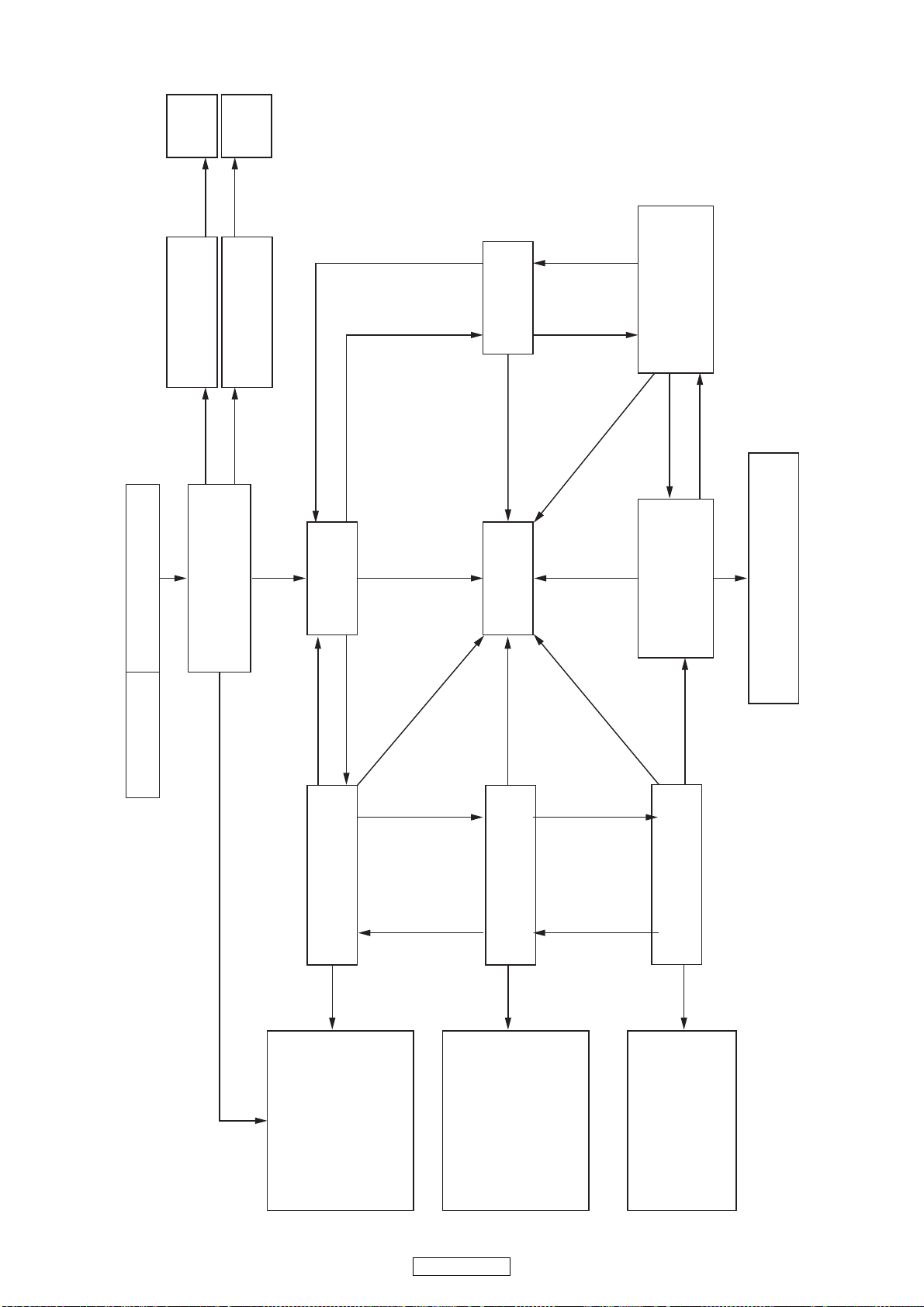
BLOCK DIAGRAM
RESET IC
(SEIKO)
80130ALMC
SPI EEPROM 4K
(ST)
M95040
MAIN MCU
(TOSHIBA)
TMP92FD23FG
9MHz
X'TAL
KEY0
KEY1
FL RST
FL DATA
FL CLK
FL CS
OPEN_SW, CLOSE_SW
CD RST
AMUTE
BUS2
BUS3
BUS CK
BUS CE
CD DSP
(TOSHIBA)
TC94A92FG
BCK
LRCK
GATE
DATA
BLOCK DIAGRAM
LD
16.9344MHz
X'TAL
FC+/TR+/-
FMG
DMG
SYS_CLK
MOTOR
DRIVER
(INTERPION)
IP4001CR
INVERTER
KIC7SH04FU
LOAD+/-
BCK/LRCK/A_OUT
SPIN+/SLED+/-
F+/-,TR+/-
DAC_RST
OPEN/CLOSE
CD MECHA
(SANYO)
(BURBROWN)
AUDIO DAC
PCM1796
CD/MP3/WMA DISC
DIGITAL OUT
OP AMP
NJM2068
DB_TXD
INVERTER
TC7WHU04FU
OP AMP
NJM2068
DB_CLK
DB_RXD
DB_TXD
SYSTEM
IN/OUT
OPTICAL
OUT
AUDIO
OUT
MUTE
KEY
FLT
(SAMSUNG)
HCA-18MS03T
USB RST
DISP DATA(I2C)
USB MCU
(TOSHIBA)
TMP92CD28FG
D+/D-
IPOD
USB DEVICE
9MHz
X'TAL
USB JACK
I2CSCL
I2CSDA
AMUTE
IPOD CP 2.0b
MFI341S2161
LPP
DAC_CS
MCK_DAC
MDT_DAC
47
DCD-F107
Page 48

PRINTED WIRING BOARDS
AUDIO/POWER PCB ASSY (1/2)
48
DCD-F107
COMPONENT SIDE
Page 49

AUDIO/POWER PCB ASSY (2/2)
49
DCD-F107
FOIL SIDE
Page 50

MAIN PCB ASSY
COMPONENT SIDE
FOIL SIDE
50
DCD-F107
Page 51

NOTE FOR PARTS LIST
Parts for which "nsp" is indicated on this table cannot be supplied.
When ordering of part, clearly indicate "1" and "I" (i) to avoid mis-supplying.
Ordering part without stating its part number can not be supplied.
Not including General-purpose Carbon Chip Resistor in the P.W.Board parts list. (Refer to the Schematic Diagram for those parts.)
Parts marked with this symbol z have critical characteristics.
Use ONLY replacement parts recommended by the manufacturer.
Not including General-purpose Carbon Film Resistor in the P.W.Board parts list. (Refer to the Schematic Diagram for those parts.)
Part indicated with the mark "★" is not illustrated in the exploded view.
WARNING:
1.
2.
3.
4.
5.
6.
● Resistors
RD : Carbon
RC : Composition
RS : Metal oxide film
RW: winding
RN : Metal film
RK : Metal mixture
P : Pulse-resistant type
NL : Low noise type
NB : Non-burning type
FR : Fuse-resistor
F : Lead wire forming
2B : 1/8 W
2E : 1/4 W
2H : 1/2 W
3A : 1 W
3D : 2 W
3F : 3 W
3H : 5 W
F:±1%
G:±2%
J:±5%
K:±10%
M:±20%
Ex.: RN
Type
14K
Shape
and performance
2E
Power
182
Resistance
G
Allowable
error
FR
Others
* Resistance
1800ohm=1.8kohm18
2
Indicates number of zeros after effective number.
2-digit effective number.
1.2ohm1R 2
2-digit effective number, decimal point indicated by R.
1-digit effective number.
: Units: ohm
● Capacitors
CE : Aluminum foil
electrolytic
CA : Aluminium solid
electrolytic
CS : Tantalum electrolytic
CQ : Film
CK : Ceramic
CC : Ceramic
CP : Oil
CM: Mica
CF : Metallized
CH : Metallized
HS : High stability type
BP : Non-polar type
HR : Ripple-resistant type
DL : For change and discharge
HF : For assuring high requency
U : UL part
C : CSA part
W : UL-CSA part
F : Lead wire forming
0J : 6.3 V
1A : 10 V
1C : 16 V
1E : 25 V
1V : 35 V
1H : 50 V
2A : 100 V
2B : 125 V
2C : 160 V
2D : 200 V
2E : 250 V
2H : 500 V
2J : 630 V
F:±1%
G:±2%
J:±5%
K:±10%
M:±20%
Z:±80%
: - 20%
P : +100%
C:±0.25pF
D:±0.5pF
= : Others
Ex.: CE
Type
04W
Shape
and performance
1H
Dielectric
strength
3R2
CapacityMAllowable
error
BP
Others
・ Units:μF.
2200μF22
2
Indicates number of zeros after effective number.
2-digit effective number.
・ Units:μF.
2.2μF2R
2
2-digit effective number, decimal point indicated by R
1-digit effective number.
* Capacity (electrolyte only)
・ When the dielectric strength is indicated in AC,"AC" is included after the dieelectric strength value.
* Capacity (except electrolyte)
・ Units:pF
2200pF=0.0022μF22
2
Indicates number of zeros after efective number.
(More than 2)
2-digit effective number.
・ Units:pF
220pF22
1
2-digit effective number.
Indicates number of zeros after effective numver.
(0 or 1)
51
DCD-F107
Page 52

PARTS LIST OF P.W.B. UNIT
* Parts for which "nsp" is indicated on this table cannot be supplied.
* The parts listed below are for maintenance only, might differ from the parts used in the unit in appearances or dimensions.
MAIN PCB ASS'Y
Ref. No. Part No. Part Name Remarks Q'ty New
SEMICONDUCTORS GROUP
IC11 943243006920D I.C , MCU (512K,LQFP-100P)
IC12 943239007300S I.C , RESET 3.0V (50ms,C-MOS,SOT23-5P)
IC13 943249006970S I.C , EEPROM (4K,SO8-8P)
IC14 943239006900S
IC15 943243006930D I.C , USB DECODER FLASH(100PIN, QFP)
IC16 236710022502S
IC17 943245006980S
IC20 90M-HC900160R I.C , REGULATOR(SOT-223)
IC71 943239007340S IC , DCDC Converter (3.5A, SOP8)
IC81 943239006810S I.C , Single Inverter (USV)
Q202 00D9430058908 CHIP T.R
I.C , 5-CH MOTOR DRIVE IC (WITH REG,SSOP-28P)
I.C , CP CHIP (MF134IS2161,20P,FROM MARANTZ)
I.C , CD DSP (SERVO,AMPLIFIER,DSP,LQFP-80P)
NOTE :
When update Firmware,
please confirm a last
version in SDI.
Use the service board after
updating it.
CVIANAM1494C
CVIS80130ALMCJAPT2
CVIM95040-WMN6TP
CVIIP4001CRLTF
CVIANAM1495C
CVI236710022502S_M
CVITC94A92FG
CVIKIA1117S15
CVISI8005QTL
CVIKIC7SH04FU
HVTKTA1504SYRTK
*
*
*
D201,202 00D9430060404 SCHOTTKEY BARRIER DIODE
D206 00D2760717903 DIODE 1SS355T
D701 943204006840S SCHOTTKY DIODE (40V,3A, DO-214AC)
CAPACITORS GROUP
C101,102 nsp CHIP CAP
C103-105 nsp CHIP CAP
C106 nsp CHIP CAP
C107,108 nsp CHIP CAP
C109 nsp CHIP CAP
C110 nsp CHIP CAP (18PF/50V)
C111 nsp CHIP CAP (18PF/50V)
C112 nsp CHIP CAP
C113,114 nsp CHIP CAP
C115-117 nsp CHIP CAP
C118 nsp CHIP CAP
C151 nsp CHIP ELECT CAP
C201 nsp CHIP CAP
C202,203 nsp CHIP CAP
C204 nsp CHIP CAP
C205 nsp CHIP CAP
C206 nsp CHIP CAP
C207 nsp CHIP CAP
C208 nsp CHIP CAP
C210 nsp CHIP CAP
C211 nsp CHIP CAP
C213 nsp CHIP CAP
C214 nsp CHIP CAP
C215 nsp CHIP CERAMIC CAP (1608, 5600p)
C216 nsp CHIP CAP
C217 nsp CHIP CAP
C219 nsp CHIP CAP
C220-222 nsp CHIP CAP
C223 nsp CHIP CAP
C224 nsp CHIP CAP
C225 nsp CHIP CAP
C226 nsp CHIP CAP
HVDRB160L60TE25
HVD1SS355T
CVDSS34SR
CCUS1H104KC
CCUS1H103KC
CCUS1H102KC
CCUS1H104KC
CCUS1H103KC
CCUS1H180JA
CCUS1H180JA
CCUS1H104KC
CCUS1H103KC
CCUS1H104KC
CCUS1A105KC
HCEC0JRV2101T
CCUS1H222KC
CCUS1H104KC
CCUS1H103KC
CCUS1H472KC
CCUS1H104KC
CCUS1H153KC
CCUS1H104KC
CCUS1H104KC
CCUS1H104KC
CCUS1H104KC
CCUS1H333KC
CCUS1H562KC
CCUS1H471JA
CCUS1H473KC
CCUS1H473KC
CCUS1H104KC
CCUS1H103KC
CCUS1H470JA
CCUS1H153KC
CCUS1H103KC
52
DCD-F107
Page 53

Ref. No. Part No. Part Name Remarks Q'ty New
C227 nsp CHIP CAP
C231 nsp CHIP CAP
C232,233 nsp CHIP CAP
C234 nsp CHIP CAP
C235 nsp CHIP CAP
C236 nsp CHIP CAP
C237 nsp CHIP CAP
C238 nsp CHIP CAP
C239 nsp CHIP CAP
C240 nsp CHIP CAP
C243-247 nsp CHIP CAP
C256-260 nsp CHIP CAP
C265 nsp CHIP CAP
C268-271 nsp CHIP CAP
C281,282 nsp CHIP ELECT CAP
C284-290 nsp CHIP ELECT CAP
C292-295 nsp CHIP ELECT CAP
C501-504 nsp CHIP CAP
C510,511 nsp CHIP CAP
C512 nsp CHIP CAP
C513 nsp CHIP CAP (18PF/50V)
C514-520 nsp CHIP CAP
C531-533 nsp CHIP CAP
C534 nsp CHIP CAP
C535 nsp CHIP CAP
C536 nsp CHIP CAP
C537 nsp CHIP CAP
C538 nsp CHIP CAP
C539 nsp CHIP CAP
C540 nsp CHIP CAP
C541 nsp CHIP CAP
C542 nsp CHIP CAP
C551-557 nsp CHIP ELECT CAP
C601 nsp CHIP CAP
C602 nsp CHIP CAP
C603 nsp CHIP CAP
C604 nsp CHIP CAP
C605 nsp CHIP CAP
C606 nsp CHIP CAP
C610 nsp CHIP CAP
C611 nsp CHIP CAP
C612 nsp CHIP CAP
C613 nsp CHIP CAP
C614 nsp CHIP CAP
C615 nsp CHIP CAP
C616 nsp CHIP CAP
C617 nsp CHIP CAP
C618 nsp CHIP CAP
C619 nsp CHIP CAP
C620 nsp CHIP CAP
C621 nsp CHIP CAP
C701 nsp
C702 nsp CHIP CAP
C703 nsp CHIP CAP
C705,706 nsp CHIP CAP
C707 nsp CHIP CAP
SMD ELECT CAP (MANLEX, RV, 25V/220, 8X10) CCEC1ERV221T
CCUS1H471JA
CCUS1H102KC
CCUS1H104KC
CCUS1H102KC
CCUS1H104KC
CCUS1H102KC
CCUS1H104KC
CCUS1H102KC
CCUS1H103KC
CCUS1H104KC
CCUS1H104KC
CCUS1H104KC
CCUS1H104KC
CCUS1H104KC
HCEC0JRV2101T
HCEC0JRV2101T
HCEC0JRV2101T
CCUS1H104KC
CCUS1H104KC
CCUS1H220JA
CCUS1H180JA
CCUS1H104KC
CCUS1H104KC
CCUS1H103KC
CCUS1H104KC
CCUS1H103KC
CCUS1H104KC
CCUS1H103KC
CCUS1H104KC
CCUS1H103KC
CCUS1H104KC
CCUS1H103KC
HCEC0JRV2101T
CCUS1H103KC
CCUS1H104KC
CCUS1H102KC
CCUS1H103KC
CCUS1H104KC
CCUS1H102KC
CCUS1H103KC
CCUS1H104KC
CCUS1H102KC
CCUS1H103KC
CCUS1H104KC
CCUS1H102KC
CCUS1H103KC
CCUS1H104KC
CCUS1H102KC
CCUS1H103KC
CCUS1H104KC
CCUS1H102KC
CCUS1H104KC
CCUS1H221JA
CCUS1H103KC
CCUS1H104KC
53
DCD-F107
Page 54

Ref. No. Part No. Part Name Remarks Q'ty New
C708 nsp
C711 nsp CHIP CAP
C712 nsp CHIP CAP
C713,714 nsp CHIP CAP
C801 nsp CHIP CAP (12PF/50V/COG/1608)
C802 nsp CHIP CAP
C803 nsp CHIP ELECT CAP
C804 nsp CHIP CAP
OTHERS PARTS GROUP
BK51 nsp PCB BRACKET
BK52 nsp PCB BRACKET
SMD ELECT CAP (MANLEX RV, 16V/470, 10X10) CCEC1CRV471T
CCUS1H104KC
CCUS1H103KC
CCUS1H104KC
CCUS1H120JA
CCUS1H220JA
HCEC0JRV2101T
CCUS1H104KC
CMD1A569
CMD1A569
BN81 nsp 3P SHIELD WIRE ASS'Y(100mm, 2.0mm)
CN12 nsp WAFER , SMD (2MM PITCH)
CN21 nsp WAFER , CARD CABLE SMD
CN22 nsp WAFER , SMD (2MM PITCH)
CN23 nsp WAFER , SMD (2MM PITCH)
CN51 nsp WAFER , SMD (2MM PITCH)
CN52 nsp WAFER , SMD (2MM PITCH)
CN53 nsp
CN71 nsp WAFER , SMD (2MM PITCH)
CX11 nsp
CX12 nsp WAFER, CARD CABLE (SMD)
z F101 943661006910S POLY SWITCH (1.6A, 8V)
L101 nsp CHIP FERRITE BEAD(60ohm, 2012)
L201-206 nsp CHIP FERRITE BEAD(60ohm, 2012)
L207 nsp AXAIL COIL
L501,502 nsp CHIP FERRITE BEAD(60ohm, 2012)
L701 943472007310S POWER COIL (47UH/3A)
L702 943472007320S POWER COIL (22UH/3A)
WAFER, 20022WS-NN Series, 2mm, SMD, Vertical, 11p
WAFER, 10022H Series, 1mm, SMD, Vertical, 21p CJP21GA193ZY
CWB1B503100EN001
CJP06GA208ZY
CJP16GA193ZY
CJP06GA208ZY
CJP05GA208ZY
CJP05GA208ZY
CJP06GA208ZY
CJP11GA208ZY
CJP05GA208ZY
CJP15GA193ZY
CBA5H1600PSUYT
CLZ9R001Z
CLZ9R001Z
HLQ02C101JT
CLZ9R001Z
CLQ13E470MRZ
CLQ13E220MRZ
*
*
*
R813 nsp FERRITE BEAD (HCB2012KF-151T20 150ohm)
X101 943141001200S SMD CRYSTAL (9MHZ, HC-49/SMD, 5PF)
X501 943141001200S SMD CRYSTAL (9MHZ, HC-49/SMD, 5PF)
X801 943141001190S
SMD CRYSTAL (16.9344MHZ, HC-49/SMD, 12PF) COX16934E120S
54
DCD-F107
CLZ9R013Z
COX09000E150S
COX09000E150S
*
*
*
Page 55

AUDIO/POWER PCB ASS'Y
Ref. No. Part No. Part Name Remarks Q'ty New
SEMICONDUCTORS GROUP
IC31 00D2623362903 I.C , PCM1796DBR (DAC,FROM DENON)
IC41-43 00D9430007108 I.C , OP AMP
IC71 943239007350S I.C , SURGE ABSORBER(SC-59)
IC72 943239007350S I.C , SURGE ABSORBER(SC-59)
IC81 90M-HC300780R I.C , REGULATOR +8V
IC95 00D2622944946 I,C , REGULATOR(3.3V SMD Type)
IC96 00D2623489909 I.C , INVERTER(CMOS)
IC91 00D2631100018 I.C , REGULATOR +6V
IC92 00MHC3990699F I.C , -6V REGULATOR (TO220IS)
IC93 00D2631243001 I.C , REGULATOR(TO220IS-4)
IC94 00D9430126102 REGULATOR, +5V
CVI00D2623362903_D
HVINJM2068MDTE1
CVINSAD500F
CVINSAD500F
HVIKIA7808API
BVIBA33BC0FP
CVITC7WHU04FU
HVIKIA7806API
CVIKIA7906PI
CVIKIA78D33PI
HVIKIA7805API
*
*
*
Q301 00D2730464901 CHIP T.R
Q302 00D2690184907 CHIP T.R
Q304 00D2690192902 CHIP T.R
Q401-404 00D2730460905 CHIP T.R
Q701 00D2690184907 CHIP T.R
Q703 00D2690192902 CHIP T.R
Q901 00D9430058908 CHIP T.R
Q902 00D2730464901 CHIP T.R
Q903 00D9430058908 CHIP T.R
z Q904 943219006820S T.R
z Q905 00D2730464901 CHIP T.R
Q908,909 00D2730464901 CHIP T.R
D302 00Çc9430209400 RECT DIODE
D701 00D9430106203 2COLOR LED
D903 00D9430087607 ZENER DIODE
D305,306 00D2760717903 CHIP DIODE
D898 00D2760717903 CHIP DIODE
D901,902 00D2760717903 CHIP DIODE
D904 00D9430087607 ZENER DIODE
D905 00D9430086404 DIODE
D906-909 00D9430182502 RECT DIODE
D910,911 00D2760717903 CHIP DIODE
D912-915 00D9430182502 RECT DIODE
D917,918 00D9430182502 RECT DIODE
D920-923 00D9430041902 SCHOTTKY DIODE
D924,925 00D9430182502 RECT DIODE
D926 00D9430106106 ZENER DIODE
D927 943202005890S ZENER DIODE
D928 00D2760760905 ZENER DIODE
D929 00D2760717903 CHIP DIODE
D930,931 00D9430041902 SCHOTTKY DIODE
D933 00D9430041902 SCHOTTKY DIODE
D934,935 00D9430182502 RECT DIODE
D936,937 00D2760717903 CHIP DIODE
D950 00D9430086404 DIODE
HVTKTC3875SYRTK
HVTKRA102S
HVTKRC102S
HVTKTC2875B
HVTKRA102S
HVTKRC102S
HVTKTA1504SYRTK
HVTKTC3875SYRTK
HVTKTA1504SYRTK
CVTKTC1027YT
HVTKTC3875SYRTK
HVTKTC3875SYRTK
CVD1N4003SRT
HVDSPR39MVW3
HVDMTZJ6.2BT
HVD1SS355T
HVD1SS355T
HVD1SS355T
HVDMTZJ6.2BT
HVD1SS133MT
CVD1N4003ST
HVD1SS355T
CVD1N4003ST
CVD1N4003ST
HVD1N5819T
CVD1N4003ST
HVDMTZJ33BT
HVDMTZJ9.1BT
HVDMTZJ3.6BT
HVD1SS355T
HVD1N5819T
HVD1N5819T
CVD1N4003ST
HVD1SS355T
HVD1SS133MT
*
CAPACITORS GROUP
C301,302 nsp CHIP CAP
C303,304 nsp CHIP CAP
C305,306 nsp CHIP CAP
C307 nsp CHIP CAP
CCUS1H104KC
CCUS1H103KC
CCUS1H104KC
CCUS1H101JA
55
DCD-F107
Page 56

Ref. No. Part No. Part Name Remarks Q'ty New
C308 nsp CERAMIC CAP (100PF/50V)
C309 nsp CHIP CAP
C310 nsp CHIP CAP
C311 00D9430185402 ELECT CAP (ELNA RFO 100uF/25V)
C312-314 nsp CHIP CAP
C315 943134005040S ELECT CAP (ELNA RFOII 50V/220uF)
C318 00D2544692901 ELECT CAP (10uF/63V RFO)
C319 nsp CERAMIC CAP
C320 nsp CHIP CAP
C321 00D9430185402 ELECT CAP (ELNA RFO 100uF/25V)
C322,323 nsp CHIP CAP
C324 nsp CHIP CAP
C326 nsp CHIP CAP
C327 nsp CHIP CAP
C328 nsp CHIP CAP
C329 nsp CHIP CAP
C330 nsp CHIP CAP
C331 nsp CHIP CAP
C332 nsp CHIP CAP
C333 nsp CHIP CAP
C334 nsp CHIP CAP
C335 nsp CHIP CAP
C338 00D2544694912 ELECT CAP (220uF/25V, RFO)
C339 nsp CHIP CAP
C340,341 00D2544694912 ELECT CAP (ELNA, RFO, 50V/22UF)
C342,343 nsp CHIP CAP
C405-408 nsp POLYPROPYLNE CAP (100V/1000PF)
C409,410 nsp CHIP CAP
C411,412 943134006940S ELECT CAP (47uF/50V, ROA, 10X16)
C415,416 nsp CHIP CAP
C417-419 nsp CHIP CAP
C422 nsp CHIP CAP
C423,424 00D2544693939 ELEC CAP ELNA RFO SERIES 100uF/50V
C701-703 nsp CHIP CAP
C704 nsp CHIP CAP
C705,706 nsp CHIP CAP
C707 nsp ELECT CAP
C708 nsp CHIP CAP
C709 nsp ELECT CAP
C711 nsp CERAMIC CAP
C712 nsp ELECT CAP
C713 nsp CERAMIC CAP
C714,715 nsp CERAMIC CAP
C717-719 nsp CHIP CAP
C720 nsp CHIP CAP
C721-726 nsp CHIP CAP
C727 nsp ELECT CAP
C728,729 nsp CERAMIC CAP
C875 nsp CHIP CAP
C876 nsp ELECT CAP
C877 nsp ELECT CAP
C878,879 nsp CHIP CAP
C882 nsp CHIP CAP
C883 nsp CHIP CAP
C893,894 nsp CHIP CAP
C895 nsp ELECT CAP
CCBS1H101KBT
CCUS1H101JA
CCUS1H104KC
CCEA1ERFO101T
CCUS1H104KC
CCEA1HRFOII221E
CCEA1JRFO100T
CCBS1H104ZFT
CCUS1H104KC
CCEA1ERFO101T
CCUS1H104KC
CCUS1H103KC
CCUS1H104KC
CCUS1H103KC
CCUS1H104KC
CCUS1H103KC
CCUS1H104KC
CCUS1H103KC
CCUS1H104KC
CCUS1H103KC
CCUS1H104KC
CCUS1H103KC
CCEA1ERFO221T
CCUS1H104KC
CCEA1HRFO220T
CCUS1H104KC
CCMP2A102JN09T
CCUS1H103KC
CCEA1HROA470T
CCUS1H103KC
CCUS1H821JA
CCUS1H821JA
CCEA1HRFO101T
CCUS1H104KC
CCUS1H103KC
CCUS1H104KC
CCEA1CKS470T
CCUS1H104KC
CCEA1CKS470T
CCBS1H104ZFT
CCEA1HKS100T
CCBS1H103ZFT
CCBS1H104ZFT
CCUS1H101JA
CCUS1H103KC
CCUS1H104KC
CCEA0JKS221T
CCBS1H104ZFT
CCUS1H104KC
CCEA1CKS101T
CCEA1AH470T
CCUS1H470JA
CCUS1H104KC
CCUS1H103KC
CCUS1H104KC
CCEA1AH101T
s
s
*
s
s
56
DCD-F107
Page 57

Ref. No. Part No. Part Name Remarks Q'ty New
C896 nsp CHIP CAP
C897 nsp CHIP CAP
C898 nsp CERAMIC CAP
C899 nsp CERAMIC CAP
C900 nsp ELECT CAP
C901 nsp CHIP CAP
C902 nsp CHIP CAP
C903 nsp CHIP CAP
C904 nsp CHIP CAP
C905 nsp CHIP CAP
C906 nsp CHIP CAP
C909 nsp CHIP CAP
C910 nsp CHIP CAP
C912 nsp CERAMIC CAP
C913 nsp ELECT CAP
C914 nsp CHIP CAP
C915 nsp CHIP CAP
C917 nsp POLYPROPYLNE CAP (100V/1500PF)
C920 nsp POLYPROPYLNE CAP (100V/1500PF)
C922 nsp CHIP CAP
C923,924 nsp CHIP CAP
C925 nsp CHIP CAP
C926 nsp CERAMIC CAP (1000PF/50V)
z C927 nsp CHIP CAP (2012 SIZE)
C932,933 nsp ELECT CAP
C934,935 nsp CHIP CAP
C936,937 nsp CHIP CAP
C938,939 nsp ELECT CAP
C940 nsp CHIP CAP
C941 nsp CHIP CAP
C942 nsp CHIP CAP
C943 nsp CHIP CAP
C944 nsp CHIP CAP
C945 nsp CHIP CAP
C946 nsp ELECT CAP
z C951 nsp CHIP CAP (2012 SIZE)
C956 nsp ELECT CAP
C957,958 nsp CHIP CAP
C959 nsp ELECT CAP
C960,961 nsp CHIP CAP
C962 nsp ELECT CAP
C963 nsp CHIP CAP
C964 nsp CHIP CAP
C965 nsp CHIP CAP
C966 nsp CHIP CAP
C967 nsp CHIP CAP
C968 nsp CHIP CAP
C969 nsp CHIP CAP
C970,971 nsp CHIP CAP
C972 nsp CHIP CAP
C973 nsp CHIP CAP
C974 nsp CHIP CAP
C975 nsp CHIP CAP
C976 nsp CHIP CAP
C977 nsp CERAMIC CAP
C978 nsp ELECT CAP
CCUS1H104KC
CCUS1H103KC
CCBS1H104ZFT
CCBS1H103ZFT
CCEA1CH102E
CCUS1H104KC
CCUS1H103KC
CCUS1H104KC
CCUS1H103KC
CCUS1H104KC
CCUS1H103KC
CCUS1H104KC
CCUS1H103KC
CCBS1H104ZFT
CCEA1CH100T
CCUS1H104KC
CCUS1H103KC
CCMP2A152JN09T
CCMP2A152JN09T
CCUS1H103KC
CCUS1H103KC
CCUS1H102KC
CCBS1H102KBT
CCUC2A103KC
CCEA1EH102E
CCUS1H333KC
CCUS1H104KC
CCEA1EH101T
CCUS1H104KC
CCUS1H103KC
CCUS1H104KC
CCUS1H103KC
CCUS1H104KC
CCUS1H103KC
CCEA1EH222E
CCUC2A103KC
CCEA1EH222E
CCUS1H104KC
CCEA1CH101T
CCUS1H104KC
CCEA1CH101T
CCUS1H103KC
CCUS1H104KC
CCUS1H103KC
CCUS1H104KC
CCUS1H103KC
CCUS1H104KC
CCUS1H103KC
CCUS1H104KC
CCUS1H103KC
CCUS1H104KC
CCUS1H103KC
CCUS1H104KC
CCUS1H103KC
CCBS1H103ZFT
CCEA1JH101E
*
*
57
DCD-F107
Page 58

Ref. No. Part No. Part Name Remarks Q'ty New
C979 nsp ELECT CAP
C980 nsp ELECT CAP
C981,982 nsp CHIP CAP
z C985 00D9430024408 CERAMIC CAP (X1/Y2/SC)
C986-989 nsp CHIP CAP
C990 nsp ELECT CAP
C992 nsp ELECT CAP
C993 nsp CHIP CAP
C994 nsp ELECT CAP
C995 nsp CHIP CAP
C996 nsp CHIP CAP
C997 nsp ELECT CAP
C998 nsp CHIP CAP
C999 nsp CHIP CAP
OTHERS PARTS GROUP
S701-704 00D9430004402 TACT SW
S706-708 00D9430004402 TACT SW
CCEA1HH100T
CCEA1JH101E
CCUS1H103KC
KCKDKS472ME
CCUS1H103KC
CCEA1CH222E
CCEA1HH1R0T
CCUS1H102KC
CCEA1HH1R0T
CCUS1H103KC
CCUS1H104KC
CCEA1HH100T
CCUS1H103KC
CCUS1H104KC
CST1A012ZT
CST1A012ZT
BK31 nsp PCB BRACKET
BK71,72 nsp FLT BRACKET
BK91 nsp PCB BRACKET
BN32 nsp WAFER
BN51 nsp 5P SHIELD WIRE ASS'Y(200mm, 2.0mm)
BN97 nsp 7P WIRE ASS'Y(220mm, 2.0mm)
CN12 nsp WAFER , CARD CABLE
CN32 nsp WAFER
CN53 nsp WAFER , STRAIGHT
CN71 nsp WAFER , STRAIGHT
CN81 nsp WAFER , STRAIGHT(3PIN)
CN91 nsp WAFER
CN92 nsp WAFER
CN93 nsp WAFER(YMW025-05R)
CN94 nsp WAFER
CN97 nsp LOCKING TYPE , STRAIGHT WAFER , 2MM
CY11 nsp WAFER
F701 00D3938086009 V.F.D , DCD-510AE (16ST85GINK)
CMD1A569
CMD1A468
CMD1A569
CJP15GB99ZY
CWB1C205200EG001
CWB1C90722047
CJP15GA117ZY
CJP15GA98ZY
CJP11GA19ZY
CJP05GA19ZY
CJP03GA19ZY
CJP02GA89ZY
CJP02KA060ZY
CJP05GA01ZY
CJP03GA01ZY
CJP07GI236ZW
CJP21GA117ZY
CFL16ST85GINK
JK71 943643001320S USB JACK STRAIGHT(BLACK)
JK91 00D9430183103 OPTICAL MODULE (TX)
JK92 00D9430191700 IN/OUT JACK
JK93 90M-YT004860R STEREO JACK
L701 nsp CHIP FERRITE BEAD(60ohm, 2012)
L901 nsp CHIP FERRITE BEAD(60ohm, 2012)
RY91 943101006870D RELAY , DC5V, 0.15W, DLS5D1-0.15W
z T901 943101007370S SUB TRANS 9V (EUR) DCD-F107E2
58
DCD-F107
CJJ9X006Z
HJSTOTX177L
CJJ4N034Z
CJJ2D008Z
CLZ9R001Z
CLZ9R001Z
CSL1C004ZE
CLT5I014ZE
*
*
*
Page 59

WIRING DIAGRAM
LPP
WIRING DIAGRAM
MAIN TRANS
SUB TRANS
POWER PCB
CUP122Z-1
MAIN PCB
CUP12202Z
CX12
15p FFC
15P
CN21
16P
CN22
6P
CN23
5P
CN51
5P
CX11
21P
CN53
11P
AC
CN94
3P
CN93
5P
CN92
2P
CN91
2P
CN53
11P
CN97
7P
CY11
21P
BN97
7P
21P FFC
BN51
5P
DISPLAY PCB
CUP12219Z-3
CD LOADER
AUDIO PCB
CUP12219Z-2
CN12
CN32 15P
CN81
3P
CN71
5P
BN81
3P
CN71
5P
09.05.29
USB 5V PCB
59
DCD-F107
Page 60

EXPLODED VIEW s
z
s
z
Parts marked with this symbol have critical
characteristics.
Use ONLY replacement parts recommended by
the manufacturer.
WARNING:
60
DCD-F107
Page 61

PARTS LIST OF EXPLODED VIEW
sss
4
* Parts for which "nsp" is indicated on this table cannot be supplied.
P.W.B. ASS'Y for which "nsp" is indicated on this table cannot be supplied. When repairing the P.W.B. ASS'Y, check the board parts table and order replacement parts.
*
* Part indicated with the mark " ★ " is not illustrated in the exploded view.
* The parts listed below are for maintenance only, might differ from the parts used in the unit in appearances or dimensions.
Note: The symbols in the column "Remarks" indicate the following destinations.
BK : Black model SP : Premium Silver model
Ref. No. Part No. Part Name Remarks Q'ty New
C4 nsp MAIN PCB ASS'Y
COP12202C
1*
C1A nsp AUDIO/POWER PCB ASS'Y
C1 - FRONT PCB
C6 - POWER PCB
C7 - AUDIO PCB
C8 - MAIN SUB PCB
P1 943415006250D DOOR BK
P1 943415007330D DOOR SP
P2 943416006260D WINDOW
P3 943443006270D INNER PANEL BK
P3 943443006280D INNER PANEL SP
P4 943412006290D 5P KNOB BK
P4 943412006300D 5P KNOB SP
P5 943412006310D 3P KNOB BK
P5 943412006320D 3P KNOB SP
P6 943481000370D LENS
P7 943412006330D USB CONTROL KNOB BK
P7 943412006340D USB CONTROL KNOB SP
P8 00D9430094506 FOOT
P9 00D9430094603 CUSHION
P10 00D9430095505 AC CORD BUSHING
M1 943402006420D FRONT PANEL (AL) BK
M1 943402006430D FRONT PANEL (AL) SP
M2 943412006440D POWER KNOB ASSY BK
M2 943412006450D POWER KNOB ASSY SP
M3 nsp EARTH PLATE
M4 nsp FIP BRACKET
M5 943403006460D TOP CABINET BK
M5 943403006470D TOP CABINET SP
M6 nsp PCB BRACKET
M7 nsp MAIN CHASSIS
M8 nsp MECHA.BRACKET
M9 nsp PCB BRACKET
M10 943406006480D REAR PANEL
M11 00D9430094700 RUBBER
COP12219B
CGR1A490ZB28
CGR1A490RGZG45
CGU1A440Z
CGW1A483B28
CGW1A483RGG45
CBT1A1117MBC57
CBT1A1117MBC22
CBT1A1116MBC57
CBT1A1116MBC22
CGL1A230A14
CBT1A1114MBC57
CBT1A1114MBC22
CKL1A189
CHG1A285
KHR1A028
CKM1A218ZC45
CKM1A218ZC62
CBY1A049ZA
CBY1A049YA
CMC1A371
CMD1A468
CKC2A198B49
CKC2A198G60
CMD1A724
CUA2A300
CMD1A722
CMD1A569
CKF1A407Z
CHG1A113
1*
1*
1*
1*
1*
1*
1*
1*
1*
1*
1*
1*
1*
4
4
1
1*
1*
1*
1*
1*
2*
1*
1*
1*
1*
1*
4
1*
2*
C2 943172007420D FIP
z C3 943101006510D TRANS
C5 943302000090D MECHANISM
C5 943302012231S CD MECHA CJDWSL11TCNJ
z C9 00D9430180407 AC CORD
★ A1
★ A2
★ A3
★ A4
nsp WASHER
nsp WIRE ASS'Y
nsp 5P WIRE ASS'Y
nsp 11P WIRE ASS'Y
CFL16ST85GINK
CLT5M039ZE
CJDWSL11TCNA
CJA2B043ZA
CNW4A028
CWB1B005300GG
CWB1C905080EG
CWB1C911180EG
1
1*
1
1 *
1
1
1
1
1
61
DCD-F107
Page 62

Ref. No. Part No. Part Name Remarks Q'ty New
CWB5A906300GG
CWC4F1A16A100A10
CWC4F4A21A100A08
CWC4F4A15A150A08
CTBD3+8JFZR
CTBD3+8JFN
CTB3+6FFZR
CTB3+8JFZR
CTS3+8JR
CTB3+10JR
CTW3+8JR
CTB4+6FR
CTWD4+6FFZR
CTWD4+6FFN
CTB3+6JR
SCREWS
★ A5
★ A6
★ A7
★ A8
S1 nsp SCREW BK
S1 nsp SCREW SP
S2 nsp SCREW
S3 nsp SCREW
S4 nsp SCREW
S5 nsp SCREW
S6 nsp SCREW
S7 nsp TRANS SCREW
S8 nsp SCREW BK
S8 nsp SCREW SP
S9 nsp SCREW
nsp WIRE ASS'Y
943606007430S CARD CABLE
943606007440S CARD CABLE
943606007450S CARD CABLE
1
1
1
1
9
9
4
8
2
8
13
2
2
2
6
62
DCD-F107
Page 63

EXPLODED VIEW OF CD MECHANISM UNIT
11
13
12-2
14
30
30
30
6
7
8
5
10
4
1
2
3
24
21
22
23
20
19
18
17
6
25
28
26
27
13
14
12-1
30
9
63
DCD-F107
Page 64

PARTS LIST OF CD MECHANISM UNIT
* Parts for which "nsp" is indicated on this table cannot be supplied.\
* The parts listed below are for maintenance only, might differ from the parts used in the unit in appearances or dimensions.
Ref. No. Part No. Part Name Remarks Q'ty New
1 00DS264629001 Tray (C) 1
2 - - This part (No.2)doesn't belong to the tray. Take it
3 00DS262554401 Gear cover(S) 1
4 00DS262553501 Tray gear(S) 1
5 00DS262554601 Chucking plate 1
6 nsp Screw 2.6 x 7 +PTPWH 4
7 nsp Chucking yoke 1
8 nsp Magnet 1
9 00D9640011007 MECHA DA11T3CN 1
10 nsp Chucking pulley 1
11 nsp Sub chassis Ass'y 1
12-1 00DS262723601 Coil spring(front) 2
12-2 00DS262723501 Coil spring(back) 2
13 nsp Screw 2.6 x 10 +P No slit type2 4
14 nsp Washer 2130 4
17 nsp Outsert main chassis(S) 1
18 nsp Screw 2.6 x 16 +PTPWH 1
19 00DS262554701 Drive gear(S) 1
20 00DS262554504 Contorol cam(S) 1
21 00DS169266711 Leaf switch 2
22 nsp 5P connector 1
23 nsp Loading P.W.B 1
24 00DSX26251171 Loading motor Ass'Y 1
25 00DS262553402 Middle gear 1
26 00DS262553602 Loading pulley 1
27 00DS365338700 LM belt 1
28 nsp Screw 2.6 x 2.5 +B 1
30 00DS262723401 Insulator 4
down from old tray and use again when changing the tray.
64
DCD-F107
Page 65

PACKING VIEW
206
208
207
201
205
210
209
210
211
212
212
s
PARTS LIST OF PACKING & ACCESSORIES
* Parts for which "nsp" is indicated on this table cannot be supplied.
* The parts listed below are for maintenance only, might differ from the parts used in the unit in appearances or dimensions.
Note: The symbols in the column "Remarks" indicate the following destinations.
BK : Black model SP : Premium Silver model
Ref. No. Part No. Part Name Remarks Q'ty New
201 nsp POLY BAG
202 943541007520D INST MANUAL(E2)
203 nsp S.S.LIST(EX)
204 00D9430097202 STEREO MINIPLUG CORD
205 00D9430097008 2P PIN CORD
206 943535007470D POLY BAG
207 943533007480D SNOW PAD
208 943533007490D SNOW PAD
209 943531007460D OUT CARTON BOX
210 nsp POS LABEL SP
210 nsp POS LABEL BK
211 00D9430110901 CONTROL LABEL SP
211 00D9430110901 CONTROL LABEL BK
212 nsp COLOR LABEL SP
CPB1061W
CQX1A1462Z
CJS9D003Z
CJS4N019Z
CPB1A184Z
CPS1A852
CPS1A853
CPG1A898Z
CQB1A941Z
CQB1A941X
CQB1A627
CQB1A627
CQB1A882Z
-
1*
1*
1
1
1*
1*
1*
1*
1*
2*
2*
2*
2*
1*
65
DCD-F107
Page 66

NOTE FOR SCHEMATIC DIAGRAM
WARNING:
Parts marked with this symbol z have critical characteristics.
Use ONLY replacement parts recommended by the manufacturer.
CAUTION:
Before returning the unit to the customer, make sure you
make either (1) a leakage current check or (2) a line to chassis
resistance check. If the leakage current exceeds 0.5 milliamps,
or if the resistance from chassis to either side of the
power cord is less than 460 kohms, the unit is defective.
WARNING:
DO NOT return the unit to the customer until the problem is
located and corrected.
NOTICE:
ALL RESISTANCE VALUES IN OHM. k=1,000 OHM
M=1,000,000 OHM
ALL CAPACITANCE VALUES IN MICRO FARAD.
P=MICRO-MICRO FARAD
EACH VOLTAGE AND CURRENT ARE MEASURED AT
NO SIGNAL INPUT CONDITION.
CIRCUIT AND PARTS ARE SUBJECT TO CHANGE
WITHOUT PRIOR NOTICE.
66
DCD-F107
Page 67

87654321
SHEET 04
TO DISPLAY UNIT
FOR ANAM
MCU UPDATE
FOR DENON
MCU UPDATE
SHEET 04
TO MECHANISM
SHEET 04
TO MECHANISM
D_OUT SEL
INA/STLSEL
L
B
H
-LH
L
H
H
-
SPDIF
C804
0.1uF
* Version Option
R701~R715 for DCD710AE
R801~R815 for DCD-F107AE
N.C
R8080R8060R8050R8040R703
+5V_D
C533
0.1uF
C536
0.1uF
0.01uF
C619
C620
C621
GND_D
for DCD710AE
DCD-F107 : N.C
MODE
NORMAL
GND
D-OFF
D-OFF
0
N.C
R602
GND_D
+7V_DRV
+7V_DRV
C534
0.01uF
GND_DRV
+3.3V_D
+3.3V_NSW
POWER_DET
+5V_REG_SW
0.01uF
0.1uF
1000P
FG1
N.C
R701
+5V_D
GND_D
GND_D
GND_D
POWER
21
20
19
18
17
16
15
14
13
12
11
10
9
8
7
6
5
4
3
2
1
CX11
1110987654321
CJP11GA208ZY
CN53
DCD-710AE DCDF107
MDT_DAC/DXP/BU DAC_MDT
21
MCK_DAC/DXP/BU
20
DAC_CS
19
18
DAC_MD0
DXP_CS
17
BU_CS
16
15
DXP_RST
GND_D
14
BCK
13
12
GND_D
DATA
11
10
GND_D
LRCK
9
MCK_SEL
8
DAC_RST
7
GND_D
6
5
SYS_CLK
GND_D
4
SPDIF
3
GND_D
2
A_MUTE
1
DAC_MCK
TO POWER UNIT
DAC_CS
GND_D
GND_D
SCLK_A
GND_D
BCK_A
GND_D
DATA_A
GND_D
LRCK_A
GND_D
GND_D
DAC_RST
GND_D
GND_D
DBCLK
DBTXD
DBRXD
A_MUTE
SHEET 03
A
B
C
D
E
INT0
SBSY
DREQ
28TXD
USB_BOOT/
MCU_BOOT/
+5V_REG_SW+
RESET IC 3V
1uF
R267
HVIS-80130ALMC
5
2
GND_A
91
+3.3V_D
IC12
4
VDD
OUT
3
VSS
DS
NC
1
C117
GND_DGND_D GND_D
DCD710AE : R101 0 ohm
DCD-F107 : R102 0 ohm
N.C(0)
R101
R102
0(N.C)
R103
R104
R105
R106
R107
R108
N.C
R109
R110
R111
R112
R113
+3.3V_NSW.
10K
10K
R178
R179
L205
60
L206
60
C292
C257
0.1uF
100/6.3V
10K
10K
10K
R261
R262
R263
C268
C269
C270
0.1uF
0.1uF
0.1uF
GND_DRV
MCU_RST
N.C
R160
0.1uF
N.C
C152
P.KEY/REM2
P.KEY/REM
PLAY_KEY
0
OP/CL_KEY
0
LED_R
0
LED_G
0
FL_CS
0
MCU_RST
MCU_RST
FL_RST
0
FL_CLK
0
0
0
0
C258
12
10K
R180
0.1uF
MCU_BOOT/
MCU_RST
+3.3V_A
100/6.3V
GND_A
C260
GND_A
11
FL_MDT
KEY1
KEY0
C293
INSW
CLSW
OPSW
LOAD+
LOAD-
CCE
28RXD
LD_CHK
KEY1
KEY0
E
D
A
B
C
F
MO
GND_A
0.1uF
F+
T+
T-
F-
DMO
DRVMUTE
SL+
OPEN
SL-
FOO
F+
F-
CLOSE
MAIN
HOST MCU PARTS
HOST MCU
TMP92FD23AFG
R166
C114
0.01uF
0.1uF
C115
C116
0.1uF
LD-
L207
100uH
D206
1SS355T
C244
Q202
A1504S
C271
N.C
0.1uF
C110
C111
0.1uF
C112
C113
0.01uF
R164
R165
N.C
R140
R139
R138
R137
R167
R168
R169
R170
R171
R172
R173
R174
R175
R176
R177
N.C
C616
0.01uF
C617
C618
GND_A
LD_CHK
100/6.3V
LD- LD+
C294
1K
R270
R271
R272
R273
R274
VREF
N.C
N.C
C242
C241
C108
C109
0.1uF
0.01uF
0
N.C
0
15K
R155
R156
R1570R158
7071727374
X2
X1
AM1
DVSS
DREQ
BOOT
2BTXD
AM0
P77/XT2
CCE
DVCC
CHECKIN
CHECK1
CHECK2
CHECK3
28RXD
DVSS
PL3/AN11/ADTRG
PL2/AN10
PL1/AN9
PL0/AN8
PG7/AN7/KI7
PG6/AN6/KI6
PG5/AN5/KI5
PG4/AN4/KI4
PG3/AN3/KI3
AVSS/VREFL
1 2 3 4 5 6 7 8 9 10 11 12 13 14 15 16 17 18 19 20 21 22 23 24 25
R115
100K
+5V_REG_SW+
TMP92FD23AFG
HOST MCU
AVCC/VREFH
PCO/TA0IN
P.KEY/REM
PLAY_KEY
OP/CL_KEY
FL_MDT
FL_CLK
DBTXD/TX
100K
R114
P.KEY/REM
0
10K
R1170R118
R116
+3.3V_D.
PLAY_KEY
OP/CL_KEY
FL_CLK
FL_MDT
DBTXD
DBRXD
MOTOR DRIVE PARTS
C265
0.1uF
GND_A
R260
N.C
IP4001CR
SP-
SP+
FIN-R
FIN
REB
REO
8
MUTE
4
GND1
OPIN
SPIN
F+
F-
GND2
CLIN
14 13 12 11 10 9 8 7 6 5 4 3 2 1
IC14
CVIIP4001TF
2827262524232221201918171615
22p
0.1uF
1000P
R245
470
18p
0
C101
0.1uF
C103
0.01uF
X101
100K
100K
100K
100K
100K
100K
100K
100K
100K
100K
100K
100K
100K
+3.3V_A
39
39
39
39
R247
RESET
0
47K
LD_CHK
FG4
DVCC
KEY1
KEY0
9MHz
R246
R252
R248
4.7K
C102
0.1uF
C104
0.01uF
0
0
R159
75
76
77
78
79
80
81
82
83
84
85
86
87
88
89
90
91
92
93
94
95
96
97
98
99
100
C295
100/6.3V
R244
N.C
4.7K
0
BOOT_COUNT
DBTRX/RX
GND3
SL+
SL-
TIN-R
TIN
VREF
VCC2
VCC1
LD_CTL
SLIN
T+
T-
CLO
OPO
R826
DBCLK
+3.3V_NSW.+3.3V_NSW.
C118
CX12
GND_D
15
P.KEY/REM
14
PLAY_KEY
13
OP/CL_KEY
12
LED_R
11
LED_G
10
FL_CS
9
FL_RST
8
FL_CLK
7
GND_D
6
CJP15GA193ZY
FL_MDT
5
GND_D
4
KEY1
3
GND_D
2
KEY0
1
GND_D
GND
654321
BOOT
TX
RX
RESET
VCC
CN18
BOOT
GND
RX
TX
VCC
RESET
6 5 4 3 2 1
CJP06GA208ZY
CN12
GND_D
VREF
C259
0.1uF
CN21
Vc
1
VCC
2
E
3
D
4
A
5
B
6
C
7
F
8
GND
9
LD
10
VR
11
MO
12
FO+
13
TR+
14
TR-
15
FO-
16
CN22
SP+
6543215 4 3 2 1
SP-
SLED+
SLED-
LIMITSW+
LIMITSW-
CN23
CL_SW
GND
OP_SW
LOAD+
LOAD-
DOUTSEL
R1520R1530R154
INT0
SBSY
IC11
[34] DCD710AE : H
DBCLK
CONT1
N.C(22)
R1200R1210R122
CONT1
CONT2
SRAMSTB
POWER_DET
DOUT_MUTE
0
R151
616263646566676869
DOUTSEL
POWER_DET
DOUT_MUTE
DCD-F107 : L
CONT2
CONT3
E2P_DI
100K
911R0
CONT3
E2P_DI
E2P_DO
+7V_DRV
0
R258
GND_DRV
BUCK
BUCK
SRAMSTB
E2P_DO
E2P_CLK
E2P_CLK
R250
R249
RST_1
USB_RST
USB_RST
MCK_DAC/DXP/BU
MDT_DAC/DXP/BU
P57/A15
DBRXD
NC(0)
R123
10K(N.C)
R181
DCD710AE
DCD-F107
C291
47K
47K(N.C)
BU_CS
POWER
DXP_CS
MCK_SEL
DXP_RST
MAIN UNIT
0
R150
R149
R148
DXP_CS
MCKSEL
DXP_RST
BU_CS
POWER
DAC_RST
DAC_MD0
DAC_CS
P41/A01
P13/D11
USB_DET
DVSS
P.KEY/REM2
DVCC
R1250R126
100K
R124
P.KEY/REM2
CLOSE
BOLERO VERSION
MODEL
C290
100/16V
100/16V
GND_DRV
R253
N.C
6
LED_G
LED_R
P40/A0
DVCC
NMI
DVSS
BUS3
BUS2
BUS1
BUS0
E2P_CS
FL_CS
FL_RST
OPEN
CLOSE
0
OPEN
C256
GND_DRV
51525354555657585960
N.C
R182
C289
50
49
48
47
46
45
44
43
42
41
R141
40
39
38
37
36
35
34
33
32
31
30
OPSW
29
CLSW
28
INSW
27
DRVMUTE
A_MUTE
26
R134
N.C
N.C
R183
R184
R127
R128
R129
R573 R574
N.C 10K
VREF
0.1uF
R256
470
C243
100/6.3V
C246
0.1uF
R147
R136
R135
0
100K
100K
GND_D
N.C10K
N.C
C249
0.1uF
C245
GND_DRV
0
100K
R130
GND_D
N.C
C248
0.1uF
C604
C605
C606
10K
10K
N.C
N.C
0
GND_D
N.C
N.C
R254
0.01uF
1000P
+3.3V_NSW.
+3.3V_D1
R573
R574
GND_D
C247
R251
0
0.1uF
FG2
7
100/6.3V
LOAD+
LOAD-
R133
10K
N.C
0.1uF
+3.3V_NSW
47K
47K
R199
GND_D
E2P_DO
SL+
SL-
FMO
TRO
T+
T-
GND_DRV
C151
GND_D
SRAMSTB
C613
C614
C615
60
L101
C107
0.1uF
IC13
M95010
1234
VCCCS
NC
DO
47K
R294
NC
SK
DI
GND
USB PARTS
C506
0.1uF
R572
N.C
100K
R507
100K
R508
100K
R509
100K
R510
C507
0.1uF
0.01uF
0.1uF
1000P
FG2
ALL VERSION ' L / L '
CD DSP PARTS
VERSION SEL
43PIN
9
+3.3V_NSW.
5 6 7 8
47K
R506
R511
R512
R513
R575
R576
R577
42PIN
R293
MODE
L
E2
L
H
L
E3
JP
L
H
H
H
+3.3V_NSW.
N.C
R144
R142
10K
R143
R145
GND_D
0
R146
10
C106
C105
0.01uF
47K
GND_D
DVSS
26
DVCC3A
27
P10/D8
28
29
30
31
32
33
34
35
36
37
38
39
40
41
42
43
DVSS
44
DVCC3A
45
46
47
48
49
CONT1
CONT2
CONT3
50
51 52 53 54 55 56 57 58 59 60 61 62 63 64 65 66 67 68 69 70 71 72 73 74 75
N.C
N.C
N.C
N.C
N.C
N.C
0
R5140R5150R516
CONT1
CONT2
CONT3
E1C
N.C
10K
MCK_DAC/CXP/BU
MDT_DAC/DXP/BU
DAC_RST
DAC_MD0
DAC_CS
LED_G
LED_R
BUS3
BUS2
BUS1
BUS0
FL_CS
FL_RST
USB_DET
OPSW
CLSW
INSW
DRVMUTE
A_MUTE
1000P
N.C
R132
R131
47K
R198
GND_D
TMP92FD28AFG
P61/A17
CCE
BUCK
100
100
47K
R517
R518
R519
R5200R5210R5220R523
CCE
BUS0
BUCK
MAIN
C
A
D
B
F
E
MO
LD-
+1.5V_D2
100/6.3V
47K
E2P_CLK
0.1uF
C505
C553
100/6.3V
DVSS
DVCC1A
RVOUT2
IC15
USB DECODER
DCD710AE
DCD-F107
BUS1
BUS2
BUS3
BUS0
0
BUS3
BUS2
BUS1
MP
RST_1
RST_2
SRAMSTB
D202
R243
TEI
N.C
0.047u
0.047u
470P
3.3K
470P
N.C
N.C
10K
R549
C515
+1.5V_D1
47K
330K
R240
R239
TMAX
AVDD3
5600P
FOO
47K
R565
10K
R548
Q501
N.C
47P
C224
PDO
FOO
47K
R564
0.1uF
USB_OC
VDDM1
TRO
0
R202
TRO
+3.3V_D1
R550 10K
D201
R234
10K
N.C
R236
N.C
+1.5V_D2
R238
C223
0
R237
VSS
VDD1-2
/SRAMSTB
IC17
CVITC94A92FG
FMO
VSS
FMOS
GND_D
DMO
FMO
N.C
N.C
N.C
R563
R562
R561
R558
R556
R555
R554
R553
R552
R551
47K
47K
47K
R547
R546
R545
RB160L60
N.C
R235
0.01uF
/RSTMS/CCE
TEST
DMO
VDD1-3
R501
10
+3.3V_D1
0
15K
R544
+3.3V_A
VREF
CD DSP
1
100/6.3V
C213
1000P
+1.5V_D1
100/6.3V
C502
0.1uF
DVSS
R557MODEL
RST_2
100/6.3V
C282
0
P74/TA0IN
+3.3V_A
2
0
0
0
0
BOOT
USB_BOOT/
0.1uF
GND_DGND_A
C288
N.C
R526
R525
C203
0.1uF
C281
100/6.3V
C237
STREQ
DVCC38
P82/CS2
100
R527
10K
LRCK
C209
N.C
GND_A
L203
60
0.1uF
GND_D
SBSY
SBSY
STREQ
P77/X1USB
P76/USBPON
P75/USBOC
AM1
LRCK
10K
R528
TC94A92FG
C226
0.01uF
C201
2200P
C202
R201
220
0.1uF
C204
0.01uF
C205
4700P
C206
0.1uF
C207
0.015u
C208
0.1uF
3
+3.3V_A
C211
GND_A
+1.5V_D
L204
60
C238
1000P
C239
0.01uF
GND_D
INT0
DREQ
10K
R505
0
10K
C501
0.1uF
0
R504
R503
RESET
R570
12345678910111213141516171819202122232425
100
R569
INT0
99
R568
98
PC1/INT1
R567
97
R566
96
95
94
GATE
93
DATA
92
BCK
CLZ9R013Z(150)
91
I2C_SCL
90
I2C_SDA
89
nRESET
88
2BTXD
87
2BRXD
86
MODE0
85
PF1/RxD0
84
PF0/TxD0
83
DVSS
R542
82
R541
81
AM0
R540
80
D-
R539
79
D+
R538
78
R537
77
DVCC3A
76
R530
X2
X1
0
DVSS
C513
X501
9MHz
R529
C512
R531
+3.3V_D1
N.C
15K
R241
0.015u
C225
LPFN
LPFO
VCOF
PVREF
80
1234567891011121314151617181920
VCOI
RVDD3
SLCO
RFI
RFRPI
RFEQO
DCOFC
AGCI
RFO
RVSS3
FNI2
FNI1
FPI2
FPI1
TPI
TNI
VRO
AVSS3
MDI
LDO
21222324252627282930313233343536373839
RFZI
RFRP
C215
FSMONIT
C214
5
0.033u
VREF
0.1uF
R204
C219
C218
C217
C227
R203
C240
0.1uF
C216
+3.3V_D1
47K
47K
47K
C516
47K
0.1uF
R557
47K
10K
27
27
N.C
0
C514
N.C
0.1uF
18p
22p
GND_D
USB_DET
N.C
C509
VREF
C210
0.1uF
R275
R276
R277
R278
C287
C235
C236
0.1uF
GND_D
E2P_DI
C503
C551
0.1uF
0.1uF
C552
100/6.3V
C504
RVIN
RVIN
DVSS
DVCC18
RVOUT1
PG0/KI0
PG1/KI1
PG2/KI2
PG3/KI3
DVCC3A
for EMC
CLZ9R013Z
DVSS
DVCC3A
P72/SRLL8
47K
R524
0.1uF
C508
10K
R233
DOUT
+1.5V_D2
+3.3V_D1
15K
R543
+3.3V_D.
RB160L60
R242
10K
10K
10K
10K
10K
10K
10K
R227
R228
R229
R230
R231
R232
N.C
R222
N.C
R221
VDD3
61626364656667686970717273747576777879
Pio7
Pio6
BUS3
BUS2
BUS1
BUS0
BUCK
AOUT
BCK
R502
47K
R560
100
0
0
N.C
N.C
N.C
D-
LRCK
R208
R207
R206
R205
C220
10K
USB_RST
C517
GND_D
47K
R559
NRESET
28TXD
28RXD
MODE0
I2C_SDA
I2CSCL
D+
Pio12/CDMON0/AiN2
0.1uF
GATE
DATA
BCK
Pio3
Pio2
Pio1
Pio0
VSS
VDD1-2
XVDD3
XO
XI
XVSS3
DVSS3L
Pio13/CDMON1
R212
R211
R210
R209
0.1uF
28RXD
28TXD
USB_BOOT/
POWER_DET
POWER
+5V_REG_SW+
NRESET
D-
D+
I2CSCL
I2C_SDA
MODE0
USB_OC
Pio5
Pio4
Pio14/CDMON2
41 42 43 44 45 46 47 48 49 50 51 52 53 54 55 56 57 58 59 60
40
DVSS3R
CDMON3
100
100
100
100
+3.3V_D.
N.C
N.C
N.C
N.C
GND_D
APPLE CHIP 2.0b
33K
R571
C231
+3.3V_A
100/6.3V
for DCD-F107
100/6.3V
0.1uF
C510
R292
DOUT
+3.3V_D2
C519
GND_D
R532
22K
C222
0.1uF
DVDD3L
DVDD3R
N.C
1000P
C286
C554
GND_D
nRESET
+3.3V_D1
+1.5V_D2
R220
100K
R218
100K
GND_D
+3.3V_D.
C284
C221
100/6.3V
GND_D
LRCK
BCK
AOUT
L201
C232
0.1uF
100/6.3V
GND_D
L202
C234
C233
0.1uF
GND_A
GND_D
L502
L501
C518
0.1uF
0.1uF
VCC
0.1uF
C520
5
6
7
8
9
10
11 12 13 14 15
GND_D
I2C_SCL
I2C_SDA
+5V_D
F101
C511
GND_D
GND_D
R217
R216
R215
0.1uF
+3.3V_D
60
C285
60
1000P
+3.3V_D
60
60
I2C_SCL
0.1uF
R226
R225
R224
R223
R291
R214
16.934Mhz(N.C)
47K
R213
GND_D GND_D
C610
C611
C612
GND_D
47K
R533
R534
N.C
1234
20
19
MODE1
18
17
MODE0
I2C_SDA
16
VBUS
+DATA
-DATA
GND
SHIELD
CN51
0
0
0
C801
GND_D
GND_D
100
100
100
+3.3V_D.
R816
1M(N.C)
X801
12P(N.C)
R536
54321
0
100
0.01uF
0.1uF
1000P
+3.3V_D1
0
SPDIF0
DOUT_MUTE
DOUTSEL
CCE
BUCK
BUS3
BUS2
BUS1
BUS0
SPDIF0
R290
47K
R219
LRCK
BCK
DATA
R827
GATE
STREQ
DREQ
CN81
for DCD-F107
N.C(0)
R817
0(N.C)
R818
SYSCLK
0(N.C)
for DCD-F107
C802
MDT_DAC/DXP/BU
22P(N.C)
MCK_DAC/CXP/BU
DAC_CS
SBSY
DAC_MD0
LRCK0
DXP_CS
BCK0
BU_CS
DATA0
SYSCLK
SPDIF0
DXP_RST
BCK0
DATA0
LRCK0
MCK_SEL
FOR ANAM
DAC_RST
USB UPDATE
SYSCLK
CN19
VCC
DBCLK
RESET
SPDIF
DBTXD
RX
DBRXD
TX
A_MUTE
BOOT
6 5 4 3 2 1
GND
RESET
654321
VCC
TX
RX
GND
BOOT
CN52
FG3
N.C
R535
POWER PARTS
SHEET 04
TO USB UNIT
+3.3V_D.
C296
N.C(100/6.3V)
C272
N.C(0.1uF)
R289
0
R284
N.C
47
R299
USB UPDATE
+1.5V_D
+3.3V_NSW
100/6.3V
N.C(0)
N.C(0)
R281
R282
R283
321
N.C(0)
FOR DENON
100/6.3V
C557
IC18
HVITC7WH157FU N.C
N.C(47)
IC19
GND_D
R819
0(N.C)
R820
0(N.C)
R606
R605
R604
R715
R714
R713
R813
R712
R811
R710
R809
R708
R807
R706
R705
R603
R704
R803
R702
R802
R801
R601
C555
C531
GND_DRV
C541
C542
0.1uF
VCC
ST/
SEL
5 6 7 8
CVIKIC7SH04FU N.C
GND_D
R285
N.C
IC81
0
0
0
N.C
N.C
N.C
CLZ9Z013Z(150)
N.C
0
N.C
0
N.C
0
N.C
N.C
0
N.C
0
N.C
0
0
0
IC20
KIA1117S15
0.1uF
GND_D
C539
0.01uF
GND_D
N.C
A
B
Y/
GNDY
InOut
GND
C540
0.1uF
1234
GND_D
54321
SPDIF
CVIKIC7SH04FU
GND_D
R821
0
0
R814
R815
312
C532
0.1uF
0.01uF
C537
0.1uF
C601
C602
C603
GND_D
R287
+3.3V_D.
C273
R286
GND_D
N.C(0)
for DCD-F107
54321
47
N.C
R711
R8120R709
+3.3V_D
C556
100/6.3V
C538
0.01uF
0.01uF
R288
N.C(0)
N.C(0)
N.C(0.1uF)
+3.3V_D2
100/6.3V
R8100R707
C535
0.1uF
1000P
FG1
C803
GND_D
N.C
Digital out SIGNAL LINE
CD SIGNAL LINE
USB SIGNAL LINE
SCHEMATIC DIAGRAMS (1/5)
MAIN UNIT
F
DCD-F107
Page 68

SUB POWER UNIT
87654321
A
B
CN71
CJP05GA208ZY
5V_REG_SW
12345
V_OUT
V_IN
DC/DC REGUALTOR
DCD-F107 Only
+5VDD
N.C
GND
GND
PW_GND
R751
+15V
L701
47UH/3A
C711
0.1uF
C712
C713
0.1uF
C714
0.01uF
0.01uF
FG98
FG99
68K
22K
R753
R752
PW_GND
+15V
C703
0.1uF
C701
150/25V
R754
C702
IC71
7
8
SS
SI8005Q
CVISI8005QTL
BS
1 2 3 4
220P
C704
0.1uF_NC
62k
C706 0.01uF
0.01uF
C705
56
EN
COMP
VIN
SW
GND FB
L702
22UH/3A
D701
R755
CVDSS34SR
R756
PW_GND
+5VDD
1M
51K
R757
470/16V
150/16V
0.1uF
C707
C708
C709
5.1K
PCB VESRION
DCD-F107E2
DCD-F107SP
R998
R999
C
D
SCHEMATIC DIAGRAMS (2/5)
SUB POWER UNIT
DCD-F107
E
F
Page 69

87654321
A
B
C
D
E
USB SIGNAL LINE
SCHEMATIC DIAGRAMS (3/5)
POWER UNIT
DCD-F107
F
Page 70

87654321
A
B
C
D
E
USB SIGNAL LINE
SCHEMATIC DIAGRAMS (4/5)
DISPLAY UNIT
DCD-F107
F
Page 71

87654321
A
B
C
D
E
CD SIGNAL LINE
SCHEMATIC DIAGRAMS (5/5)
AUDIO UNIT
DCD-F107
s
F
 Loading...