

Page 1

e
SERVICE MANUAL
MODEL JP E3 E2 EK K2A E1C E1K EUT
Ver. 2
Please refer to the
MODIFICATION NOTICE.
DCD-A100
P P P
SUPER AUDIO CD PLAYER
For purposes of improvement, specications and design are subject to change without notice.
•
Please use this service manual with referring to the operating instructions without fail.
•
Some illustrations using in this service manual are slightly different from the actual set.
•
e
D&M Holdings Inc.
S0175-1V02DM/DG1011
Copyright 2010 D&M Holdings Inc. All rights reserved.
WARNING: Violators will be prosecuted to the maximum extent possible.
Page 2

SAFETY PRECAUTIONS
The following check should be performed for the continued protection of the customer and service technician.
LEAKAGE CURRENT CHECK
Before returning the unit to the customer, make sure you make either (1) a leakage current check or (2) a line to chassis
resistance check. if the leakage current exceeds 0.5 milliamps, or if the resistance from chassis to either side of the
power cord is less than 460 kohms, the unit is defective.
Be sure to test for leakage current with the AC plug in both polarities, in addition, in each power ON, OFF and STANDBY
mode, if applicable.
CAUTION
Please heed the points listed below during servicing and inspection.
◎Heed the cautions!
Spots requiring particular attention when servicing, such
as the cabinet, parts, chassis,etc., have cautions indicated
on labels. be sure to heed these causions and the
cautions indicated in the handling instructions.
◎Caution concerning electric shock!
(1) An AC voltage is impressed on this set, so touching
internal metal parts when the set is energized could
cause electric shock. Take care to avoid electric
shock, by for example using an isolating transformer
and gloves when servicing while the set is energized,
unplugging the power cord when replacing parts, etc.
(2) Tere are high voltage parts inside. Handle with extra
care when the set is energized.
◎ Caution concerning disassembly and
assembly!
Through great care is taken when manufacturing parts
from sheet metal, there may in some rare cases be burrs
on the edges of parts which could cause injury if ngers
are moved across them. Use gloves to protect your hands.
◎Only use designated parts!
The set's parts have specific safety properties (fire
resistance, voltage resistance, etc.). For replacement
parts, be su re t o use part s whic h have the same
poroperties. In particular, for the important safety parts
that are marked z on wiring diagrams and parts lists, be
sure to use the designated parts.
◎ Be sure to mount parts and arrange the wires
as they were originally!
For safety seasons, some parts use tape, tubes or other
insulating materials, and some parts are mounted away
from the surface of printed circuit boards. Care is also
taken with the positions of the wores omsode amd clamps
are used to keep wires away from heating and high
voltage parts, so be sure to set everything back as it was
originally.
◎Inspect for safety after servicing!
Check that all screws , parts and wires removed or
disconnected for servicing have been put back in their
original positions, inspect that no parts around the area
that has been serviced have been negatively affected,
conduct an inslat ion ch eck on the exter nal metal
connectors and between the blades of the power plug,
and otherwise check that safety is ensured.
(Insulation check procedure)
Unplug the power cord from the power outlet, disconnect
the antenna, plugs, etc., and turn the power switch on.
Using a 500V insulation resistance tester, check that the
inplug and the externally exposed metal parts (antenna
terminal, headphones terminal, input terminal, etc.) is
1MΩ or greater. If it is less, the set must be inspected and
repaired.
CAUTION
Concerning important safety
parts
Many of the electric and structural parts used in the set
have special safety properties. In most cases these
properties are difficult to distinguish by sight, and using
replacement parts with higher ratings (rated power and
withstand voltage) does not necessarily guarantee that
safety performance will be poreserved. Parts with safety
properties are indicated as shown below on the wiring
diagrams and parts lists is this service manual. Be sure to
replace them with parts with the designated part number.
(1) Schematic diagrams ...... Indicated by the z mark.
(2) Parts lists ...... Indicated by the z mark.
Using parts other than the designated
parts could result in electric shock, res
or other dangerous situations.
2
Page 3
NOTE FOR SCHEMATIC DIAGRAM
NOTE FOR PARTS LIST
WARNING:
Parts marked with this symbol z have critical characteristics. Use ONLY replacement parts recommended by the manufacture
CAUTION:
Before returning the unit to the customer, make sure you make either (1) a leakage current check or (2) a line to chassis resistance check. If the
leakage current exceeds 0.5 milliamps, or if the resistance from chassis to either side of the power cord is less than 460 kohms, the unit is defective.
WARNING:
DO NOT return the unit to the customer until the problem is located and corrected.
NOTICE:
ALL RESISTANCE VALUES IN OHM. k=1,000 OHM / M=1,000,000 OHM
ALL CAPACITANCE VALUES IN MICRO FARAD. P=MICRO-MICRO FARAD EACH VOLTAGE AND CURRENT ARE MEASURED AT NO SIGNAL
INPUT CONDITION. CIRCUIT AND PARTS ARE SUBJECT TO CHANGE WITHOUT PRIOR NOTICE.
r.
NOTE FOR PARTS LIST
1.
Parts for which "nsp" is indicated on this table cannot be supplied.
2.
When ordering of part, clearly indicate "1" and "I" (i) to avoid mis-supplying.
3.
Ordering part without stating its part number can not be supplied.
4.
Part indicated with the mark "★" is not illustrated in the exploded view.
5.
Not including General-purpose Carbon Film Resistor in the P.W.Board parts list. (Refer to the Schematic Diagram for those parts.)
6.
Not including General-purpose Carbon Chip Resistor in the P.W.Board parts list. (Refer to the Schematic Diagram for those parts.)
WARNING:
● Resistors
Ex.: RN
* Resistance
Capacitors
●
Ex.: CE
* Capacity (electrolyte only)
* Capacity (except electrolyte)
・ When the dielectric strength is indicated in AC,"AC" is included after the dieelectric strength value.
Parts marked with this symbol z have critical characteristics. Use ONLY replacement parts recommended by the manufacturer.
Type
RD : Carbon
RC : Composition
RS : Metal oxide film
RW: winding
RN : Metal film
RK : Metal mixture
2
Indicates number of zeros after effective number.
2-digit effective number.
1-digit effective number.
: Units: ohm
Type
CE : Aluminum foil
electrolytic
CA : Aluminium solid
electrolytic
CS : Tantalum electrolytic
CQ: Film
CK : Ceramic
CC : Ceramic
CP : Oil
CM: Mica
CF : Metallized
CH : Metallized
2
Indicates number of zeros after effective number.
・ Units:μF.
・ Units:pF
2-digit effective number.
2
14K
Shape
and performance
2-digit effective number, decimal point indicated by R.
04W
Shape
and performance
Indicates number of zeros after efective number. (More than 2)
2-digit effective number.
2E
Power
2B : 1/8 W
2E : 1/4 W
2H : 1/2 W
3A : 1 W
3D : 2 W
3F : 3 W
3H : 5 W
1800ohm=1.8kohm1 8
1.2ohm1 R 2
1H
Dielectric
strength
0J : 6.3 V
1A : 10 V
1C : 16 V
1E : 25 V
1V : 35 V
1H : 50 V
2A : 100 V
2B : 125 V
2C : 160 V
2D : 200 V
2E : 250 V
2H : 500 V
2J : 630 V
2200μF2 2
2200pF=0.0022μF2 2
182
Resistance
F : ±1%
G : ±2%
J : ±5%
K : ±10%
M : ±20%
3R2
CapacityMAllowable
G
Allowable
error
P : Pulse-resistant type
NL : Low noise type
NB : Non-burning type
FR : Fuse-resistor
F : Lead wire forming
error
F : ±1%
G : ±2%
J : ±5%
K : ±10%
M : ±20%
Z : ±80%
: - 20%
P : +100%
C : ±0.25pF
D : ±0.5pF
= : Others
FR
Others
BP
Others
HS : High stability type
BP : Non-polar type
HR : Ripple-resistant type
DL : For change and discharge
HF : For assuring high requency
U : UL part
C : CSA part
W : UL-CSA part
F : Lead wire forming
2
・ Units:μF.
1
・ Units:pF
2.2μF2 R
1-digit effective number.
2-digit effective number, decimal point indicated by R
220pF2 2
Indicates number of zeros after effective numver. (0 or 1)
2-digit effective number.
3
Page 4
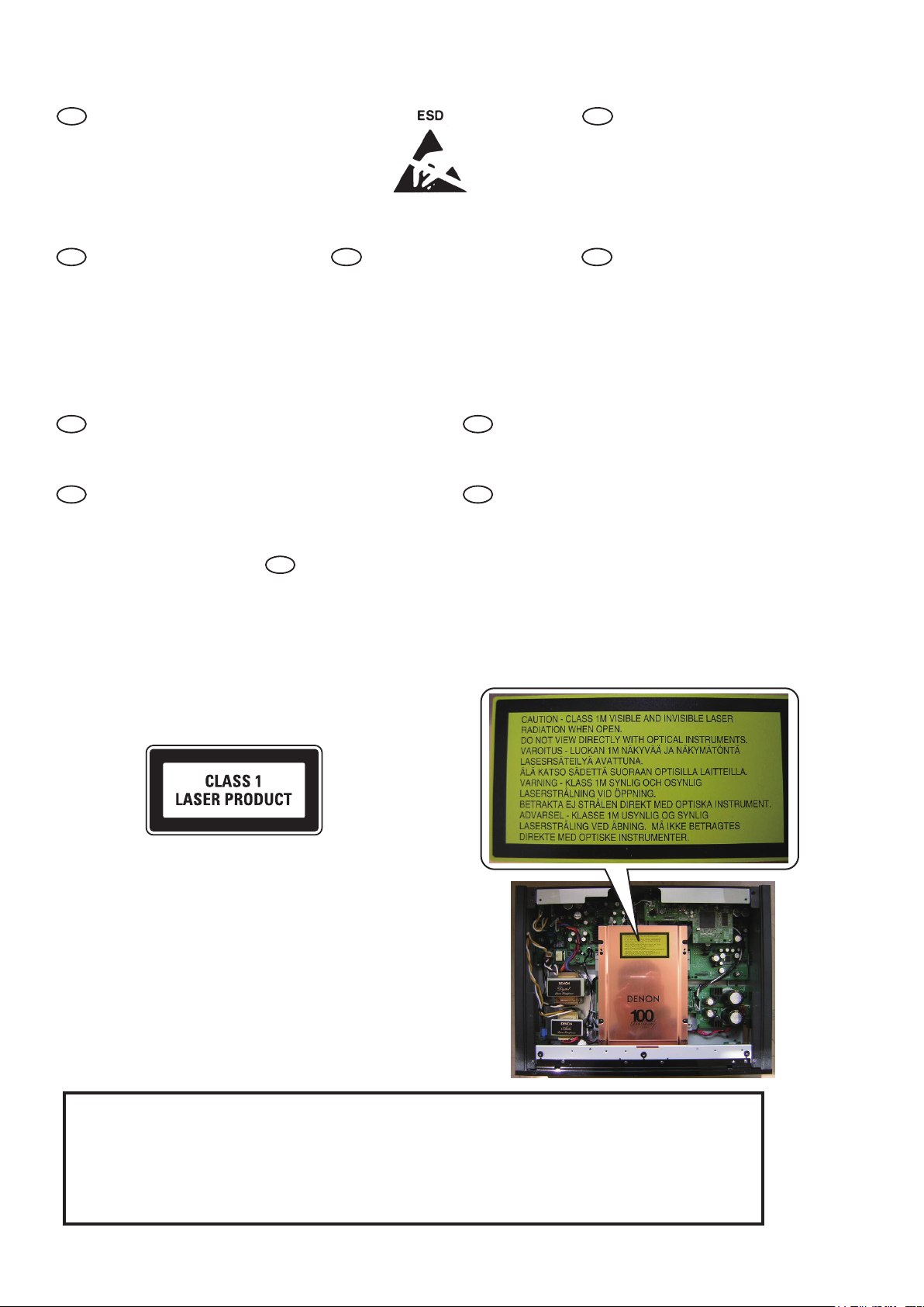
WARNING AND LASER SAFETY INSTRUCTIONS
WARNING
GB
All ICs and many other semi-conductors are
susceptible to electrostatic discharges (ESD).
Careless handling during repair can reduce life
drastically.
When repairing, make sure that you are connected
with the same potential as the mass of the set via a
wrist wrap with resistance.
Keep components and tools also at this potential.
NL
Alle IC’s en vele andere halfgeleiders zijn gevoelig
voor elektrostatische ontladingen (ESD).
Onzorgvuldig behandelen tijdens reparatie kan de
levensduur drastisch doen verminderen.
Zorg ervoor dat u tijdens reparatie via een polsband
met weerstand verbonden bent met apparaat.
Houd componenten en hulpmiddelen ook op
ditzelfde potentiaal.
WAARSCHUWING
F ATTENTION
Tous les IC et beaucoup d’autres semiconducteurs
sont sensibles aux décharges statiques (ESD).
Leur longévité pourrait être considérablement
écourtée par le fait qu’aucune précaution n’est prise
a leur manipulation.
Lors de réparations, s’assurer de bien être relié au
même potentiel que la masse de l’appareil et enfiler
le bracelet serti d’une résistance de sécurité.
Veiller a ce que les composants ainsi que les outils
que l’on utilise soient également a ce potentiel.
D
WARNUNG
Alle IC und viele andere Halbleiter sind
empfindlich gegen elektrostatische
Entladungen (ESD).
Unsorgfältige Behandlung bei der Reparatur
kann die Lebensdauer drastisch vermindern.
Sorgen sie dafür, das Sie im Reparaturfall
dem Massepotential des Gerätes verbunden
sind.
Halten Sie Bauteile und Hilfsmittel ebenfalls
über ein Pulsarmband mit Widerstand mit auf
diesem Potential.
GB
Safety regulations require that the set be restored to its original condition
and that parts which are identical with those specified be used.
NL
Veiligheidsbepalingen vereisen, dat het apparaat in zijn oorspronkelijke
toestand wordt terug gebracht en dat onderdelen, identiek aan de
gespecifieerde worden toegepast.
“Pour votre sécurité, ces document s
doivent être utilisés par des
spécialistes agrées, se uls habilités à
réparer votre appareil en panne.”
F
Les normes de sécurité exigent que l’appareil soit remis a l’état d’origine et
que soient utilisées les pièces de rechange identiques à celles spécifiées.
LASER SAFETY
This unit employs a laser. Only a qualified service person should
remove the cover or attempt to service this device, due to
possible eye injury.
I
AVVERTIMENTO
Tutti IC e parecchi semi-conduttori sono sensibili
alle scariche statiche (ESD).
La loro longevita potrebbe essere fortemente ridatta
in caso di non osservazione della piu grande
cauzione alla loro manipolazione.
Durante le riparazioni occorre quindi essere
collegato allo stesso potenziale che quello della
massa dell’apparecchio tramite un braccialetto a
resistenza.
Assicurarsi che i componenti e anche gli utensili
con quali si lavora siano anche a questo potenziale.
D
Bei jeder Reparatur sind die geltenden Sicherheitsvorschriften zu beachten.
Der Originalzustand des Gerats darf nicht verandert werden.
Fur Reparaturen sind Original-Ersatzteile zu verwenden.
I
Le norme di sicurezza esigono che l’apparecchio venga rimesso nelle
condizioni originali e che siano utilizzati pezzi di ricambiago idetici a quelli
specificati.
USE OF CONTROLS OR ADJUSTMENTS OR PERFORMANCE
OF PROCEDURE OTHER THAN THOSE SPECIFIED HEREIN
MAY RESULT IN HAZARDOUS RADIATION EXPOSURE.
AVOID DIRECT EXPOSURE TO BEAM
WARNING
The use of optical instruments with this product will
increase eye hazard.
Repair handling should take place as much as possible with
a disc loaded inside the player
WARNING LOCATION: INSIDE ON LASER COVERSHIELD
CAUTION -CLASS 1M VISIBLE AND INVISIBLE LASER RADIATION WHEN OPEN.
DO NOT VIEW DIRECTLY WITH OPTICAL INSTRUMENTS.
VAROITUS -LUOKAN 1M NÄKYVÄÄ JA NÄKYMÄTÖNTÄ LASERSÄTEILYÄ. ÄVÄTUNA.
ÄLÄ KATSUO SÄDETTÄ SUORAAN PITISILLA LAITTEILLA.
VARNING -KLASS 1M SYNLIG OCH OSYNLIG LASERSTRÅLNING VID ÖPPNING.
BETRAKTA EJ STRÅLEN DIREKT MED OPTISKA INSTRUMENT.
ADVARSEL -KLASSE 1M USYNLIG OG SYNLIG LASERSTRÅLING VED ÅBNING.
MÅ IKKE BETRAGTES DIREKTE MED OPTISKEINSTRUMENTER.
4
100301DM
Page 5
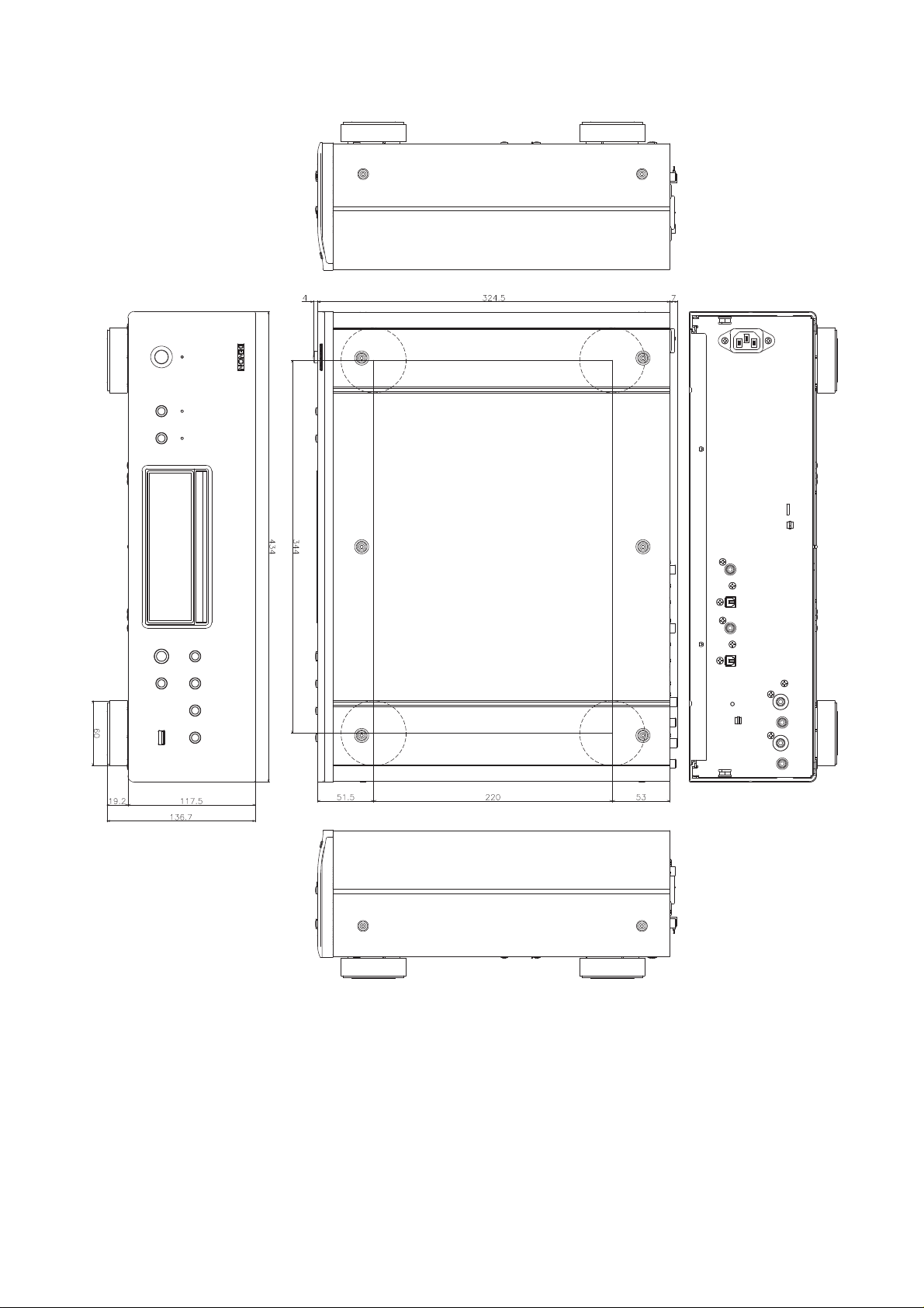
DIMENSION
5
Page 6
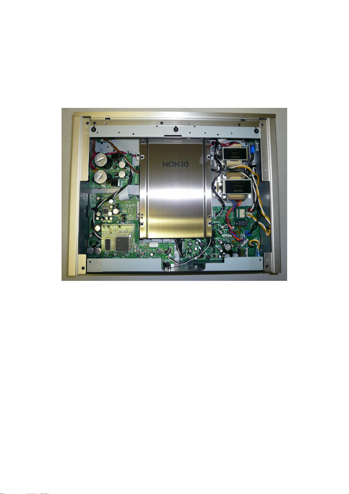
WIRE ARRANGEMENT
Front Panel side
Back Panel side
If wire bundles are untied or moved to perform adjustment or parts replacement etc.,be sure to rearrange them neatly as
they were originally bundled or placed afterward.
Otherwise, incorrect arrangement can be a cause of noise generation.
• The photograph is DCD-2010AE.
Wire arrangement viewed from the top
6
Page 7
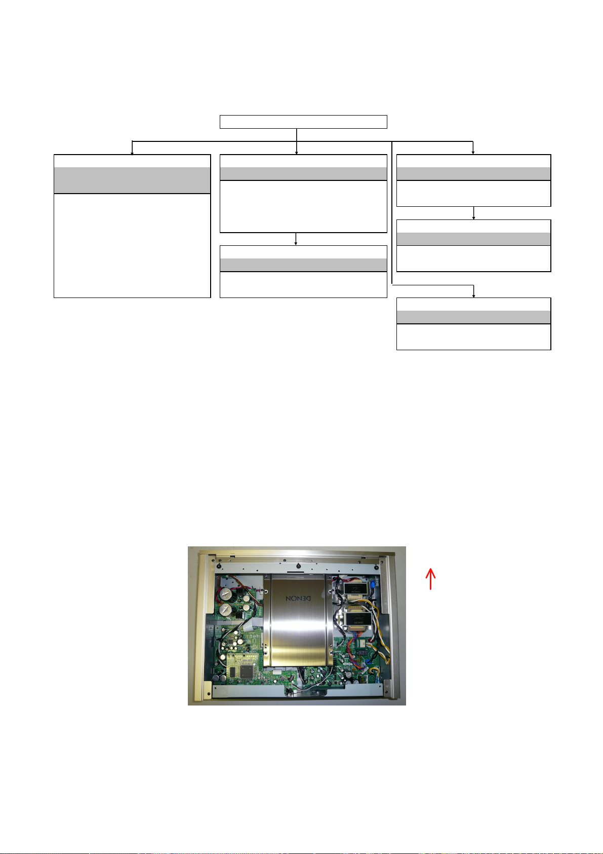
DISASSEMBLY
TOP COVER
FRONT PANEL ASSY SACD/DVD MECHA UNIT ASSY DSP/DIGITAL-IO UNIT
Refer to "DISASSEMBLY 1.FRONT PANEL ASSY" Refer to "EXPLODED VIEW" Refer to "EXPLODED VIEW"
and "EXPLODED VIEW" SACD/DVD MECHA UNIT DSP/DIGITAL-IO UNIT
ANALOG PWR UNIT (Ref. No. of EXPLODED VIEW : 3A) (Ref. No. of EXPLODED VIEW : 1)
(Ref. No. of EXPLODED VIEW : 2-2) SACD/DVD MECHA UNIT
LED UNIT (Ref. No. of EXPLODED VIEW : 3B)
AUDIO UNIT
(Ref. No. of EXPLODED VIEW : 2-4) Refer to "EXPLODED VIEW"
USB UNIT
DISPLAY UNIT
AUDIOUNIT
(Ref. No. of EXPLODED VIEW : 2-5) Refer to "EXPLODED VIEW" (Ref. No. of EXPLODED VIEW : 2-7)
D.PWR UNIT DISPLAY UNIT
(Ref. No. of EXPLODED VIEW : 2-6) (Ref. No. of EXPLODED VIEW : 2-1)
POWER SW UNIT
Refer to "EXPLODED VIEW"
POWER SW UNIT
(Ref. No. of EXPLODED VIEW : 2-3)
The viewpoint of each photograph
(Photografy direction)
[View from above]
Front side
• Disassemble in order of the arrow of the figure of following flow.
• In the case of the re-assembling, assemble it in order of the reverse of the following flow.
• In the case of the re-assembling, observe "attention of assembling" it.
About the photos used for descriptions in the “DISASSEMBLY” section.
• The direction from which the photographs used herein were photographed is indicated at "Direction of photograph: ***" at
the left of the respective photographs.
• Refer to the table below for a description of the direction in which the photos were taken.
• Photographs for which no direction is indicated were taken from above the product.
• The photograph is DCD-2010AE.
7
Page 8
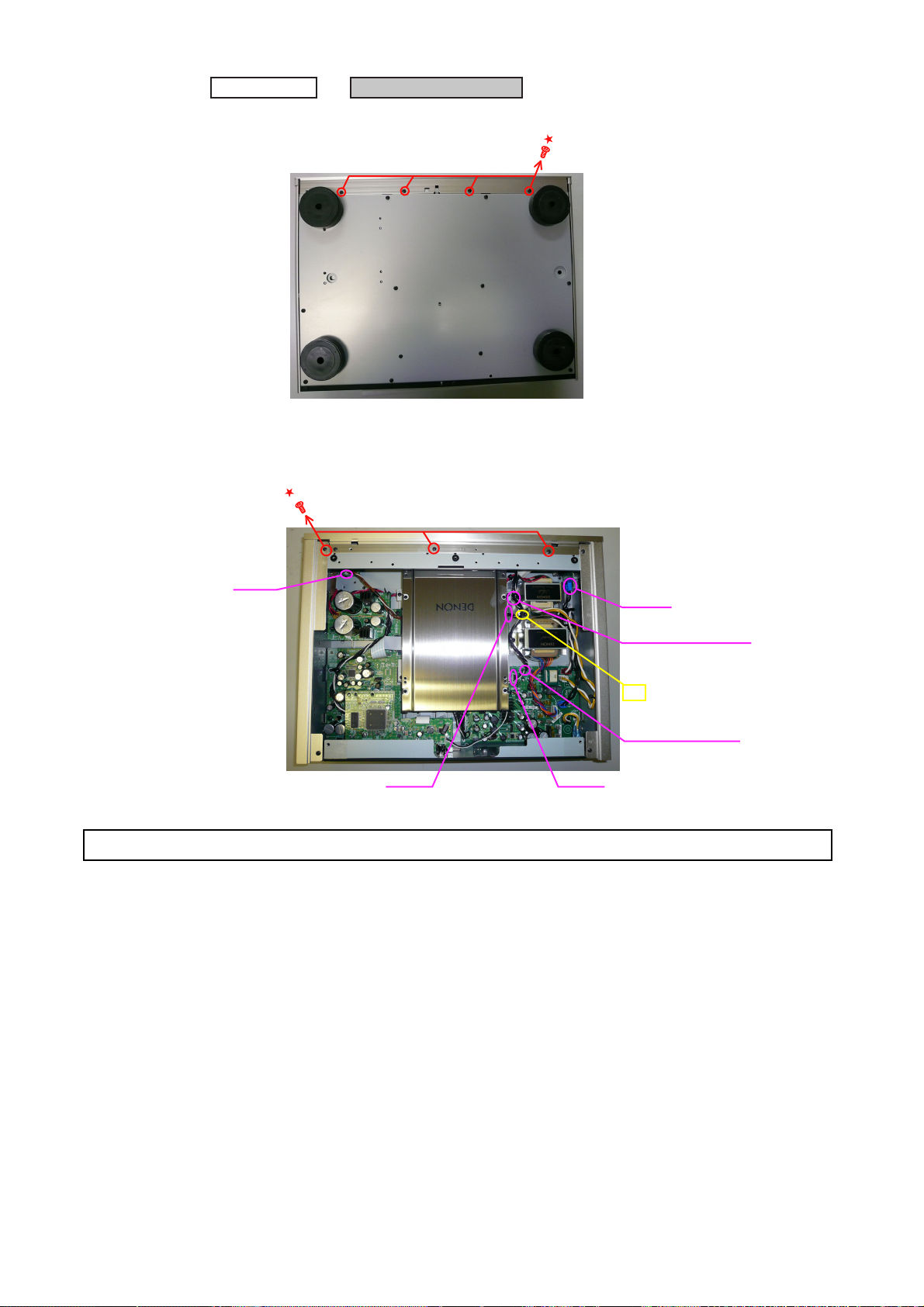
1. FRONT PANEL ASSY
Proceeding : TOP COVER
→
FRONT PANEL ASSY
View from bottom
Cord holder : Loose
CY034
Style pin : Loose
CX101 CX071
CY051
cut
Please refer to "EXPLODED VIEW" for the disassembly method of each P.W.B included in FRONT PANEL ASSY.
(1) Remove the screws.
(2) Cut the wire clamp bands, then loose the cord holder and style pin.
Disconnect the connector wires, then remove the screws.
8
Page 9
DIAGNOSTICS OF OPTICAL PICKUP AND REPLACING TRAVERSE UNIT
Make failure diagnostics of the Optical Pickup as follows.
If the laser drive current (IOP) becomes more than 1.5 times of the initial value, the Optical Pickup should be replaced.
The laser drive current initial value is checked by "IOP checked Method" of next page.
In case of replacing the Pickup, change the whole part of the Traverse Unit.
No mechanical adjustment is necessary after the replacement.
s
DVD :
(SACD)
CD :
DVD :
Laser drive current initial value:
FL Display (The display part of 13 digits)
1 2 3 4 5 6 7 8 9 10 11 12 13
- - - T 2 3 - m m m m - -
FL Display (The display part of 13 digits)
1 2 3 4 5 6 7 8 9 10 11 12 13
- - - T 2 1 - m m m m - -
FL Display (The display part of 13 digits)
1 2 3 4 5 6 7 8 9 10 11 12 13
- - - T 6 D ± m m . m - -
Disc no read, unsteady playback, etc.
Laser drive current (Iop) check
HF wave form check
(Refer to WAVE FORMS)
Present value exceeds
the initial value by 1.5
times
Mecha Unit replacing
Laser current (Iop) memorizing after replacement
Disc no read, unsteady playback, etc.
FE balance value check
DVD: over ±15 %
Mecha Unit replacing
1. IOP checked Method
Select the laser ON/OFF(CD/DVD)mode of the test mode, and check the IOP value of DVD(SACD) laser or CD laser.
1.1 DVD(SACD) laser current check
(1) Press the
(2) Check the current value of IOP (nnnn)
FL Display (The display part of 13 digits)
1 2 3 4 5 6 7 8 9 10 11 12 13
or 9 button to display the laser current value, and then select “T24”.
8
- - - T 2 4 - n n n n - -
(- : Off, DVD(SACD) laser, Initial value: Current value: nn.nn [mA])
1.2 CD laser current check
(1) Press the
(2) Check the current value of IOP (nnnn)
FL Display (The display part of 13 digits)
1 2 3 4 5 6 7 8 9 10 11 12 13
or 9 button to display the laser current value, and then select “T22”.
8
- - - T 2 2 - n n n n - -
(- : Off, CD laser, Initial value: Current value: nn.nn [mA])
9
Page 10
2. Check the FE balance value
Load the DVD (TDV-520C) in the aging mode, and then select the "T3 Servo" mode of the test mode.
Select the mode and check FE balance value.
2.1 FE balance value(DVD) check
(1) Load the DVD (TDV-520C) in the aging mode, and then select the "T3 Servo" mode of the test mode. And press the
button. The FL display shows "T6D".
8
(2) Check the FE balance value (DVD).
FL Display (The display part of 13 digits)
1 2 3 4 5 6 7 8 9 10 11 12 13
- - - T 6 D ± n n . n - -
(- : Off, FE balance value (DVD): nn.n [%])
3. Note for Handling the Laser Pick-Up
The protection for the damage of laser diode.
If you want to change the optical device unit from any other units, you must keep the following.
(1) It should be done at the desk already took measures the static electricity in care of removing the OPU's (Optical
device unit) connector cable.
(2) Workers should be put on the "Earth Band".
(3) It should be done to add the solder to the short land to prevent the broken Laser diode before removing the 24P FFC
cable.
(4) Don't touch OPU's connector parts carelessly.
4. Replacement of the Laser Pick-up (Mecha Unit)
In the following cases, change the mecha unit (FGDCD1650SES) to a new one.
(1) When the present IOP (current) value exceeds +150% of the initial value.
(2) When the FE balance value exceeds ±15% (DVD).
5. Rewriting the default value of the laser current
5.1 Store the current value of the laser current : DVD(SACD)
(1) Current value “T24” is selected.
FL Display (The display part of 13 digits)
1 2 3 4 5 6 7 8 9 10 11 12 13
- - - T 2 4 - n n n n - -
(2) Press the
FL Display (The display part of 13 digits)
1 2 3 4 5 6 7 8 9 10 11 12 13
button for at least 5 seconds, and "SAVE?" is displayed.
1/3
- - - T 2 4 S A V E ? - -
(3) Press the
FL Display (The display part of 13 digits)
1 2 3 4 5 6 7 8 9 10 11 12 13
or 9 button to select “T23”.
8
- - - T 2 3 - m m m m - -
(4) Press the
FL Display (The display part of 13 digits)
1 2 3 4 5 6 7 8 9 10 11 12 13
button and store the current value "T23". After “OK?” is displayed, stored value “T23” is displayed.
1/3
- - - T 2 3 - - O K ! - -
(5) Press the
button to display the current value “T24” without storing the current value “T23”.
2
10
Page 11
5.2 Store the current value of the laser current : CD
(1) Current value “T22” is selected.
FL Display (The display part of 13 digits)
1 2 3 4 5 6 7 8 9 10 11 12 13
- - - T 2 2 - n n n n - -
(2) Press the
FL Display (The display part of 13 digits)
1 2 3 4 5 6 7 8 9 10 11 12 13
button for at least 5 seconds, and "SAVE?" is displayed.
1/3
- - - T 2 2 S A V E ? - -
(3) Press the
FL Display (The display part of 13 digits)
1 2 3 4 5 6 7 8 9 10 11 12 13
or 9 button to select “T21”.
8
- - - T 2 1 - m m m m - -
(4) Press the
FL Display (The display part of 13 digits)
1 2 3 4 5 6 7 8 9 10 11 12 13
button and store the current value "T21". After “OK?” is displayed, stored value “T21” is displayed.
1/3
- - - T 2 1 - - O K ! - -
(5) Press the
button to display the current value “T22” without storing the current value “T21”.
2
6. Resetting the accumulated laser on time
To clear the accumulated laser on time, press the 1/3 button while the accumulated laser on time is displayed until
" * CLR?" appears at the "nnnnn" position, then press the 8 or 9 button to select TB3. If the 1/3 button is
pressed while TB3 is displayed, the accumulated laser on time of CD and DVD(SACD) is cleared.When “TB1” or “TB2”
is selected with the 8 or 9 button, "nnnnn" is displayed as 0 so you can check.
FL Display (The display part of 13 digits)
1 2 3 4 5 6 7 8 9 10 11 12 13
- - - T B Y n n n n n - -
(- : Off, Y:1: CD, 2: DVD(SACD), nnnnn: Hour [h])
11
Page 12
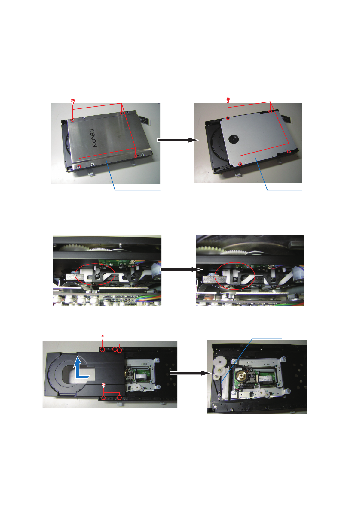
HOW TO REPLACE TRAVERSE UNIT
MECHA TOP PLATE GUIDE-CLAMP
BELT LOAD
Caution: The optical pickup can be damaged easily by static electricity charged on human body. Take necessary
anti-static measures when repairing around the optical pickup.
(Follow the procedure below in reverse order when reassembling.)
• The photograph is DCD-2010AE.
1. MECHA TOP PLATE GUIDE-CLAMP disassembly
(1) Remove 4 screws, then detach MECHA TOP PLATE.
(2) Remove 4 screws, then detach GUIDE-CLAMP.
2. Tray disassembly
(1) Push in the SLIDE CAM side underneath the MECHA front slowly securely. The Tray can now be pulled out.
(2) Pull out the tray, remove 5 screws of the tray rear. Remove the tray to direction of the arrow.
※ Check there is grease on the BELT LOAD. If there is grease on the BELT LOAD, wipe it off with alcohol.
12
Page 13
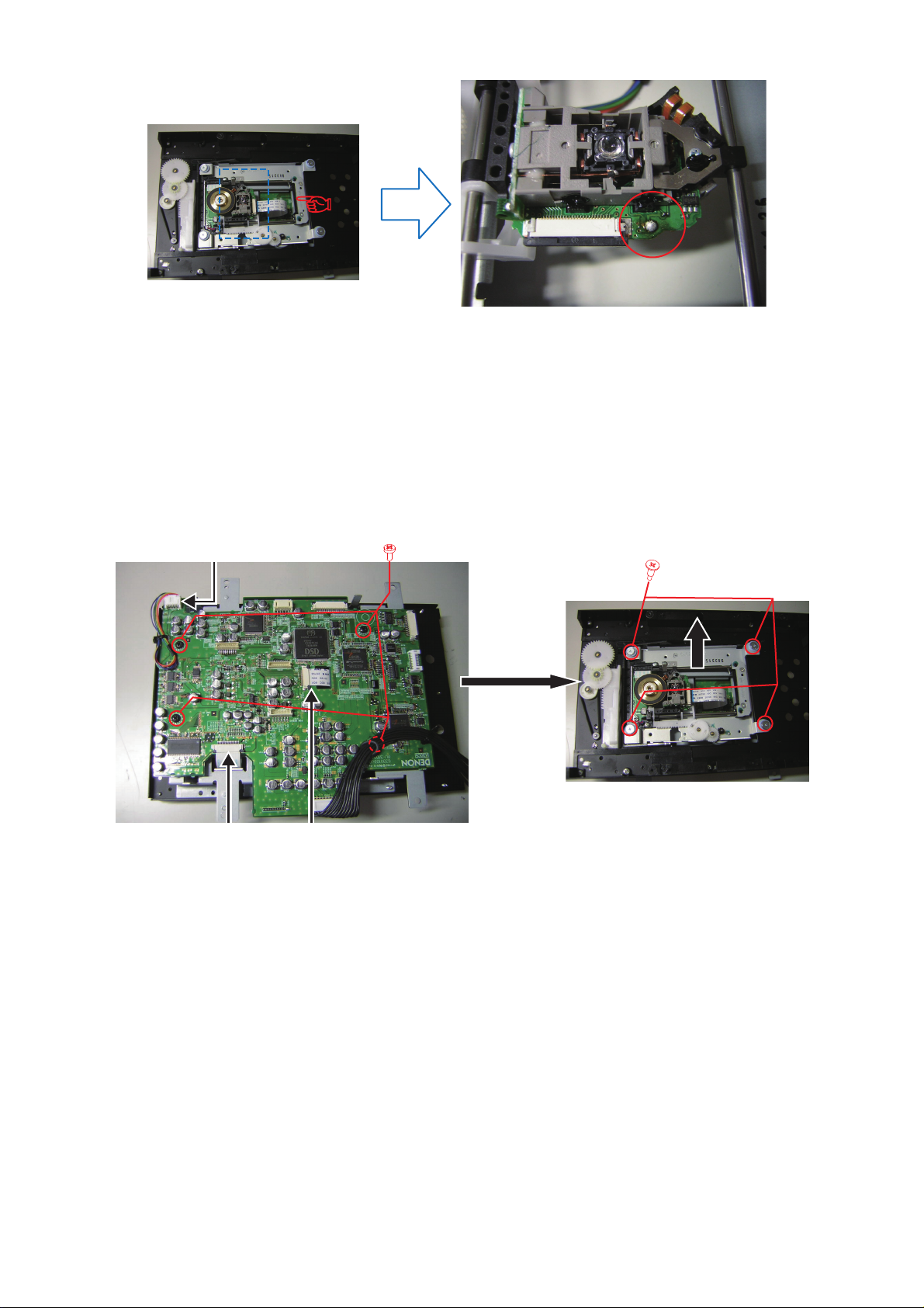
(3) Solder the short-circuit.
5P PH
15P FFC 24P FFC
3. Traverse Unit disassembly
(1) Remove 15P FFC, 24P FFC and 5P PH WIRE connecting with from the MECHA P.W.B. UNIT.
(2) Remove 4 screws then detach MECHA P.W.B. UNIT.
(3) Remove 4 screws fixing DAMPER.
(4) Remove Traverse Unit in the arrow direction.
13
Page 14
SPECIAL MODE TRANSITION DIAGRAM
H.R.NORMAL operation
TOC read → playback
title-all of the disc. →
OPEN → CLOSE →
TOC read
It displays repeatedly.
H.R.SHORT operation
TOC read → playback
title-end of the disc. →
OPEN → CLOSE →
TOC read
It displays repeatedly.
H.R.CHACKING operation
TOC read → OPEN →
CLOSE → TOC read
It displays repeatedly.
1/3
1/3
1/3
H.R.NORMAL MODE
“NORMAL”
89
H.R.SHORT MODE
“SHORT”
89
H.R.CHACKING MODE
“CHACKING”
Heat run Error Code Table
No Error contents FL display
1 Tray Error ERROR 01
2 Bad Disc
3 Search Error
4 Read Error
9
8 or 1/3
ERROR 02
ERROR 03
ERROR 04
2 + 5 + POWER_ON
AGING MODE
“Aging Mode”
※ The tray opens and stops.
If loading an SACD, do not
carry out the next operation
until the title display ends
and “Aging Mode” is
displayed again.
2
TEST MODE
“Test Mode”
9
SERVICE MODE
1. Initial Setting Mode
1.1. procedure
(1)InitializetheCDplayerwhenμcom,peripheralpartsofμcom,orP.W.B.hasbeenreplacedinservicing.
(2)Allusersettingwillbelostanditsfactorysettingwillberestoredwhenthisinitializationismade.Besuretomemorize
yoursettingforrestoringagainaftertheinitialization.
(3)Carryoutthefollowingtorestorefactorysettingmode.
POWERswitchisturnedtoonwhilepressingthe
Display"RESET"ontheFLtube,thenkeeppressingthetwobuttonsuntil"RESET"turnsoff.
and
2
buttonssimultaneouslyonthemainunit.
9
14
Page 15
2. Version display
3. Test mode
3.1. Entering the test mode
To enter the test mode, press the 9 button in the heat run mode.
Basically, the test mode should be set in the stop mode after the disc is loaded in the heat run mode.
(The heat run mode is entered by pressing the 2 and 5 buttons simultaneously to turn on the POWER switch.
When the heat run mode is set, the “PLAY” and “PAUSE” indicators light.)
2.1. procedure
(1)POWERswitchisturnedtoonwhilepressingthe
1/3
and
theFLtube.Next,theversionofthesystemμcomisdisplayedonFLtube.
(2)Now,pressthe9button,followinginformationisdisplayedontheFLtube.
Display Order
<
>
VersionofBootLoader→VersionofB/E→MakedayofB/E→VersionofFPGA→VersionofUSBμ-com→
ChecksumcheckresultofEEPROM(Referetob1)→CommunicationresultwithB/E(Referetob2)→Theentire
FLtubeisashingwithanintervalofabout1second.
1ChecksumcheckresultofEEPROM
b
"EEPOK"
normal
:
"EEPErr1":Tuner/Timer-relatedchecksumerror
"EEPErr2":Amp-relatedchecksumerror
"EEPErr3":LastLine1,2selectchecksumerror
2CommunicationresultwithB/E
b
"BEOK"
normal
:
"BEErr":Communicationerror
buttonssimultaneously."Ver.Disp"isdisplayedon
8
3. Test mode
3.1. Entering the test mode
Toenterthetestmode,pressthe
Basically,thetestmodeshouldbesetinthestopmodeafterthediscisloadedintheheatrunmode.
(Theheatrunmodeisenteredbypressthe2and
Whentheheatrunmodeisset,the"1"and"3"indicatorslight.
buttonintheheatrunmode.
9
buttonssimultaneouslytoturnonthePOWERswitch.
5
Press 2 and 5 buttons simultaneously
POWER SW(h)
9 button
Test mode
8 or /1 3 button
Heat run mode
/
1 3 button
Excuting Heatrun
FLtubedisplaywhentestmodeentered
FLDisplay(Thedisplaypartof13digits)
1 2 3 4 5 6 7 8 9 10 11 12 13
- - - T e s t M o d e - -
ThediscsplayableintheHeartRunModearethediscsshownonthetable.
Playable
discs
DVD-Audio DVD-Video Video CD CD CD-R CD-RW
DVD-R
DVD+R
DVD-RW
DVD+RW
SUPER
AUDIO CD
Mark
(logo)
15
Recordable
Page 16

3.2. Selecting the mode
Thefollowingmodesareavailable.
・
Pressthe8or9buttontoselecteachmodeandpressthe
Pressthe2buttontoreturntothemodeoriginallysetwhenthetestmodewasentered.
(1)FLtubelightingmode : T0
(2)Trayopen/closemode : T1
(3)Laseron/off(CD/DVD)mode : T2
(4)Servoadjustmentvaluedisplaymode : T3
(5)Tracemode(errorratedisplay) : T7
(6)Servopropertiesmeasurementmode : TA
(7)Accumulatedlaserontimedisplaymode : TB
(8)Monitorterminalsettingmode : TD
(9)SACDwatermarksignalqualitycheckingmode: TE
(10)Selftestmode : TF
buttontosetthatmode.
1/3
16
Page 17
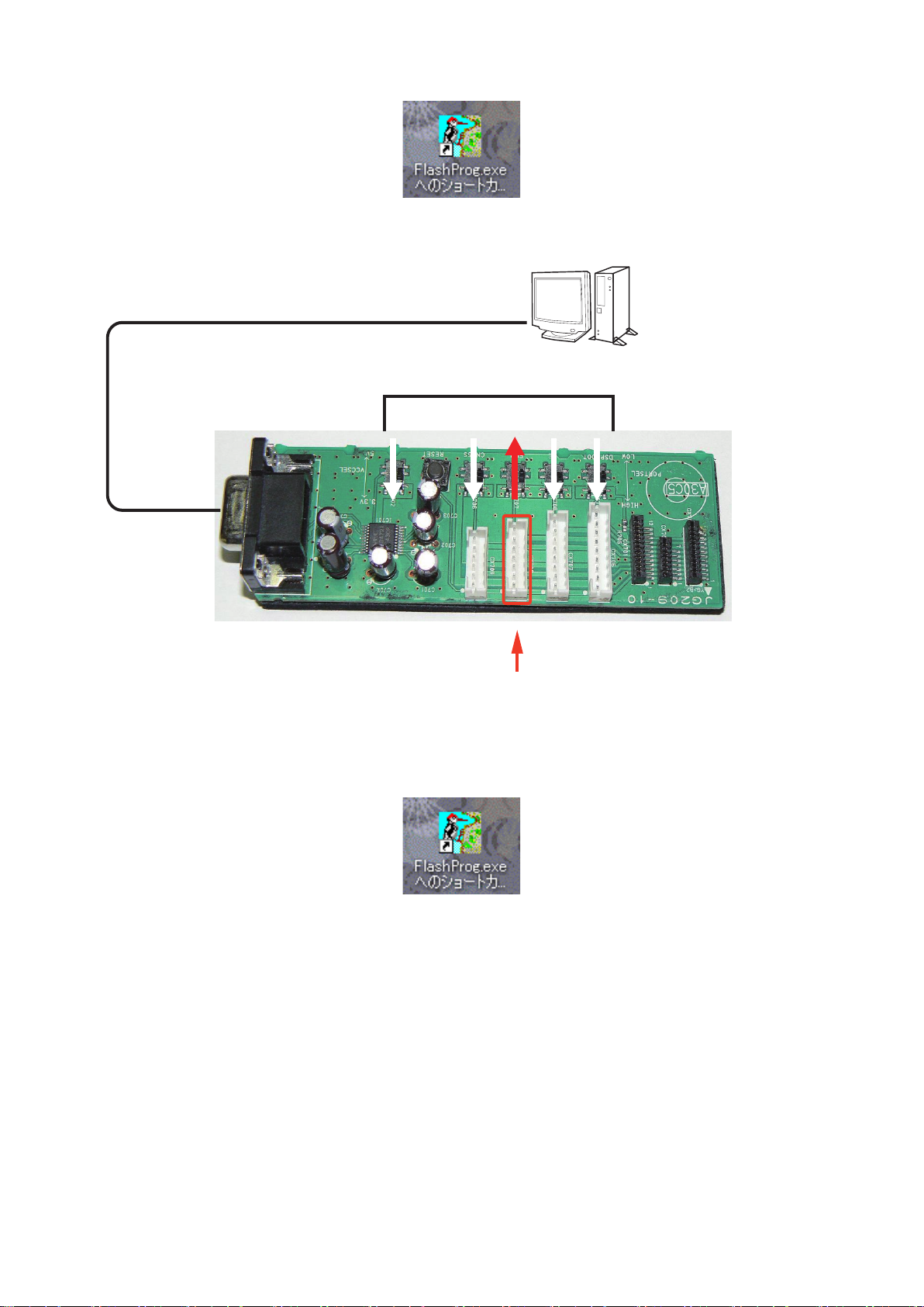
4.VERSION UPGRADE PROCEDURE OF FIRMWARE
PC
①Connect windows PC with RS-232C cable.
②Switch to the direction of the arrow.
③Connect CX072 on the 8U-310040 board
with 7P PH-PH CONN.CORD(00D2042971069)
④Turn on DCD-2010AE.
(Check connection CY141 on 8U-310040.)
⑤Press the RESET button.
CX708
S706
(CNVSS)
4.1. Update for IC502(M3062LFGPGP)
(1) PreparethewindowsPCthatinstalledtheFLASHSTA.EXE.
(2) ConnectSPK-581asfollows.
(3) DoubleclicktheFLASHSTA.EXE.AndlaunchtheM16FlashStart.
17
Page 18
(4) ChecktheInternalashmemoryintheSelectProgram.
ChoosetheCOMPortnumber.
AndclicktheOK.
(5) ClicktheRefer....
(6) ChoosetheDCD-1650SE.mot.AndclicktheOpen.
18
Page 19
(7) TheFilePathandIDareinputtedautomatically,andtheMCUTypeisselectedtoM16C/2062automatically.
ClicktheOK.
(8) ClicktheSetting....
19
Page 20
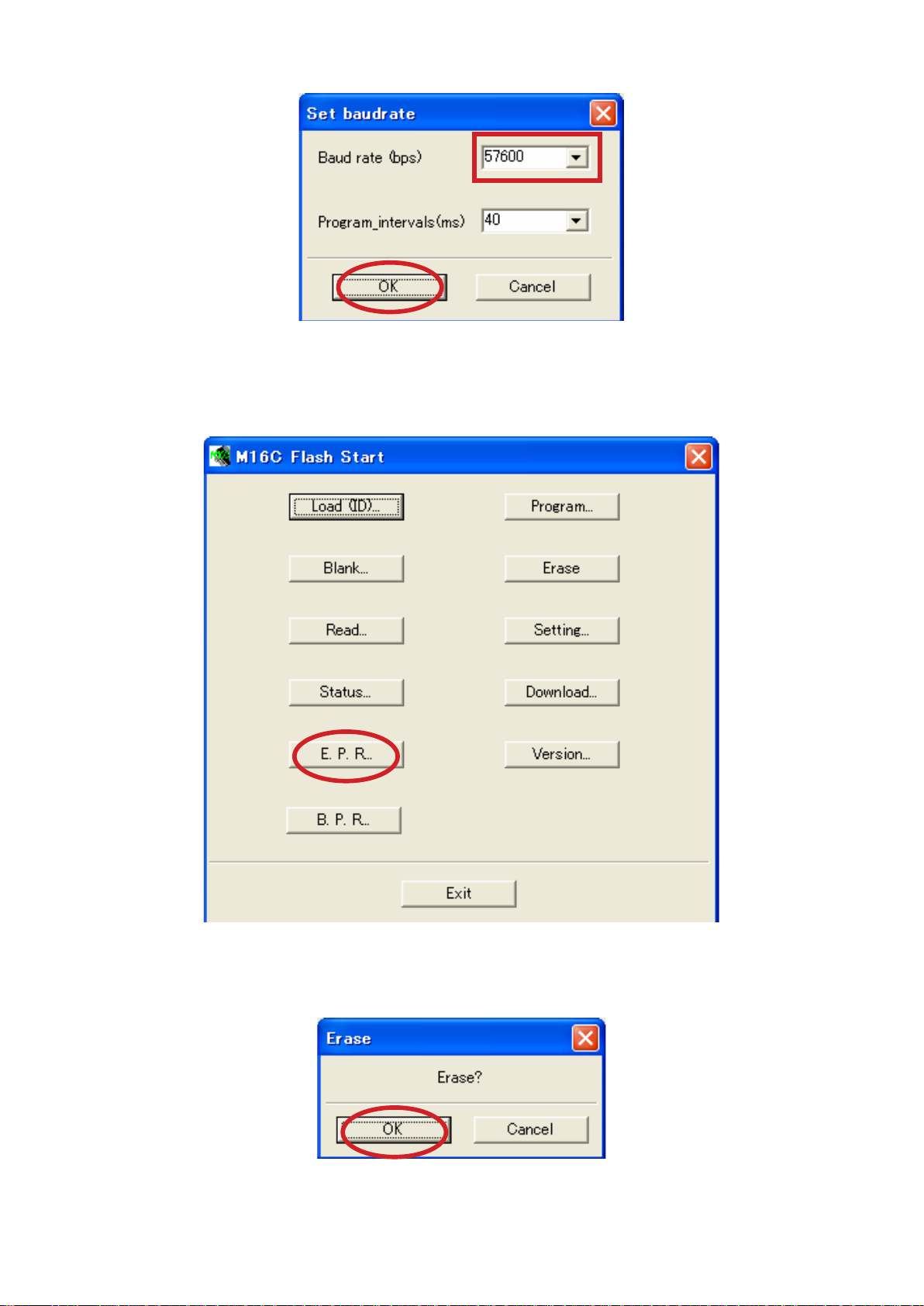
(9) Choosethe57600intheBaudrate.(DONOTchoosetheotherone!!)
ClicktheOK.
Thesettingismemorizedifitdoesonce.
※
Itisnecessarytosetittoconnectedfailureagainwhendoing.
(10)ClicktheE.P.R....
(11)ClicktheOK.
20
Page 21
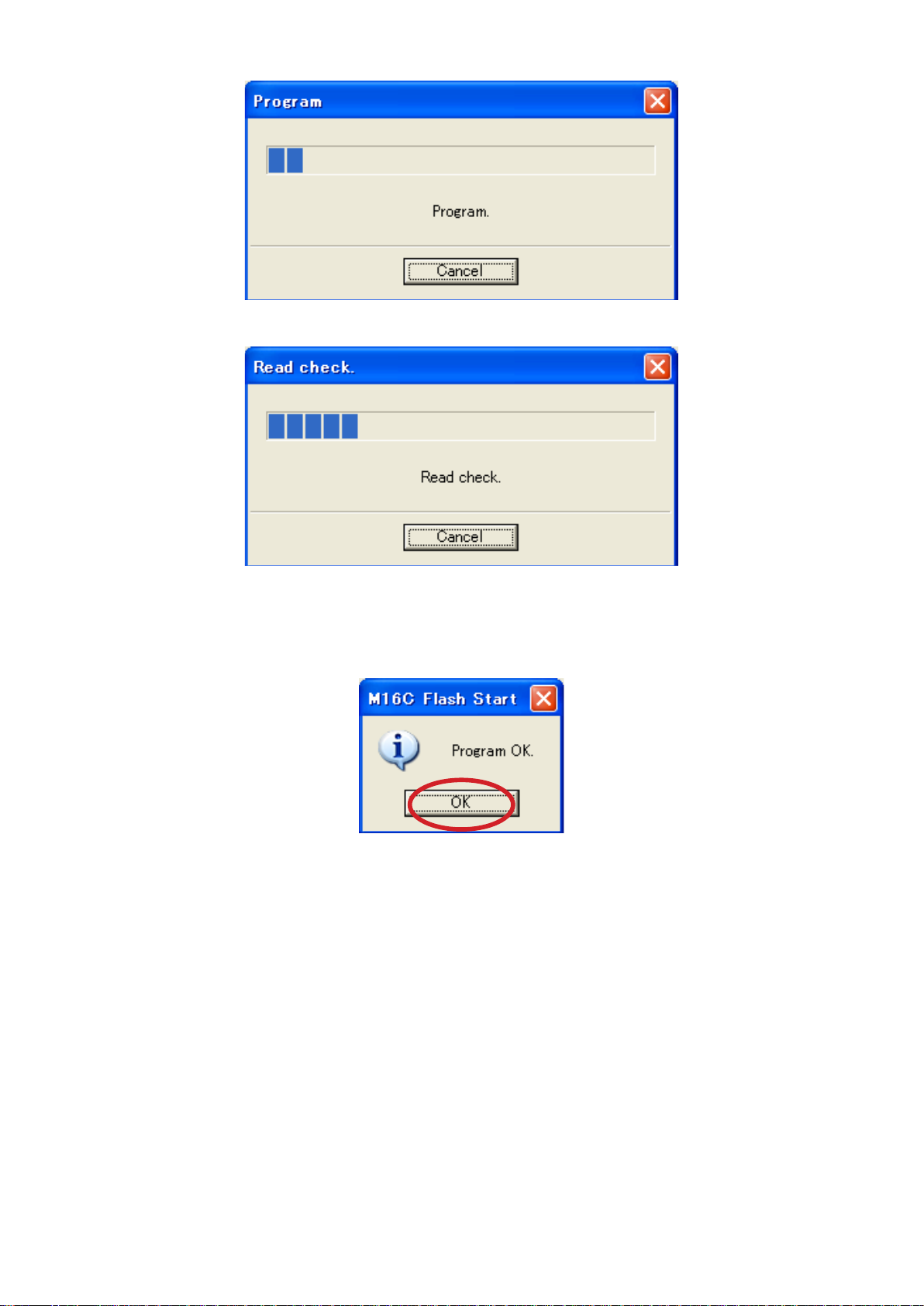
(12)SoftwareiswrittenintotheI-nternalFlash-ROM.
Thewritingofsoftwaretakesabout1minute30seconds.
Thecheckingofsoftwaretakesabout50seconds.
(13)ClicktheOK.
Pleaseretryitfrom(8)whenfailing.
21
Page 22
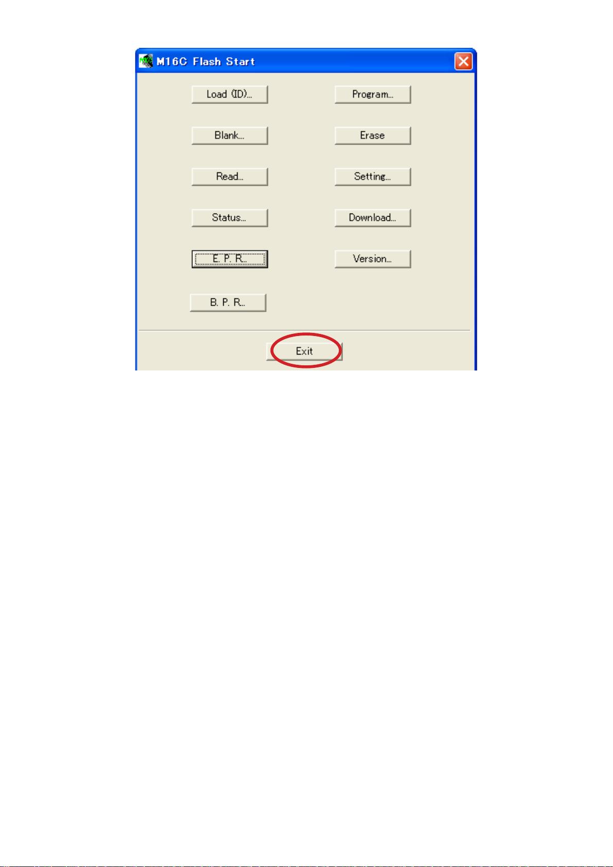
(14)ClicktheExit.
(15)TurnoffDCD-A100.
(16)RemovetheSPK-581formDCD-A100.
22
Page 23
4.2.UpdateforIC803(TMP92FD28AFG)
PC
①Connect windows PC with RS-232C cable.
②Switch to the direction of the arrow.
③Connect CX072 on the 8U-310040 board
with 7P PH-PH CONN.CORD(00D2042971069).
CX708
(1) PreparethewindowsPCthatinstalledtheFlashProg.EXE.
(2) ConnectSPK-581asforrows.
(3) DoubleclickFlashProg.exe,andlaunchtheFlashProgrammer.
23
Page 24
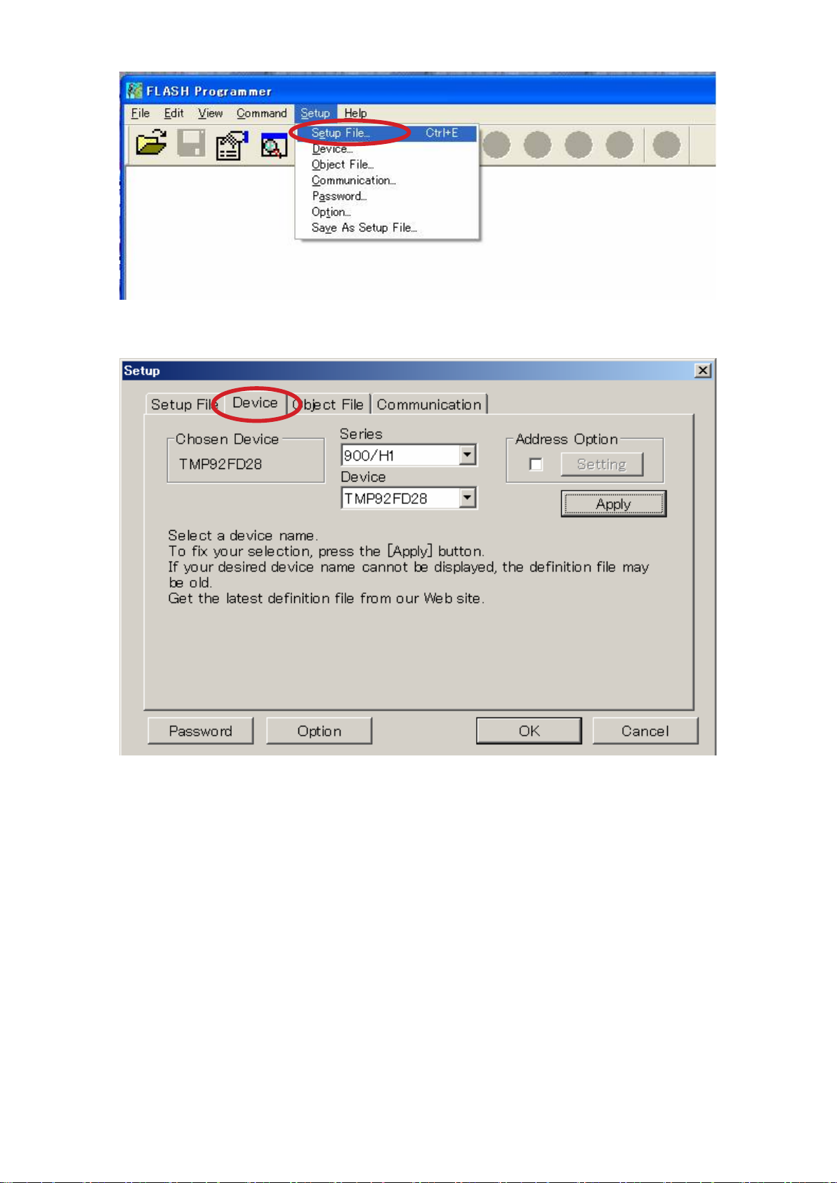
(4) ClicktheSetupinthemenubarandselecttheSetupFile.
(5) ClickDevicetab.
24
Page 25
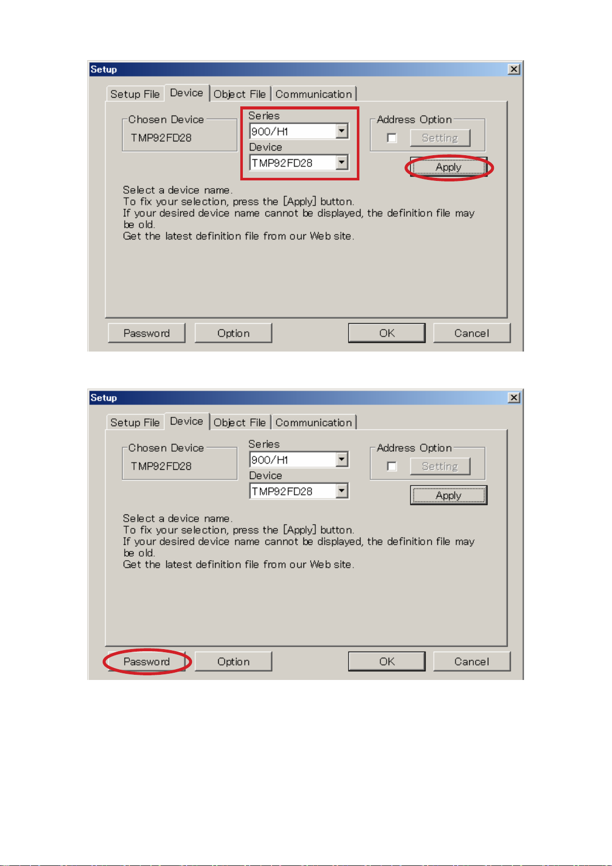
(6) ChoosetheTMP91FD28intheDevice,andchoosethe900/H1intheSeries.
ClickApply,anddisplaythechosenDvice.
(7) ClickPassword.
25
Page 26
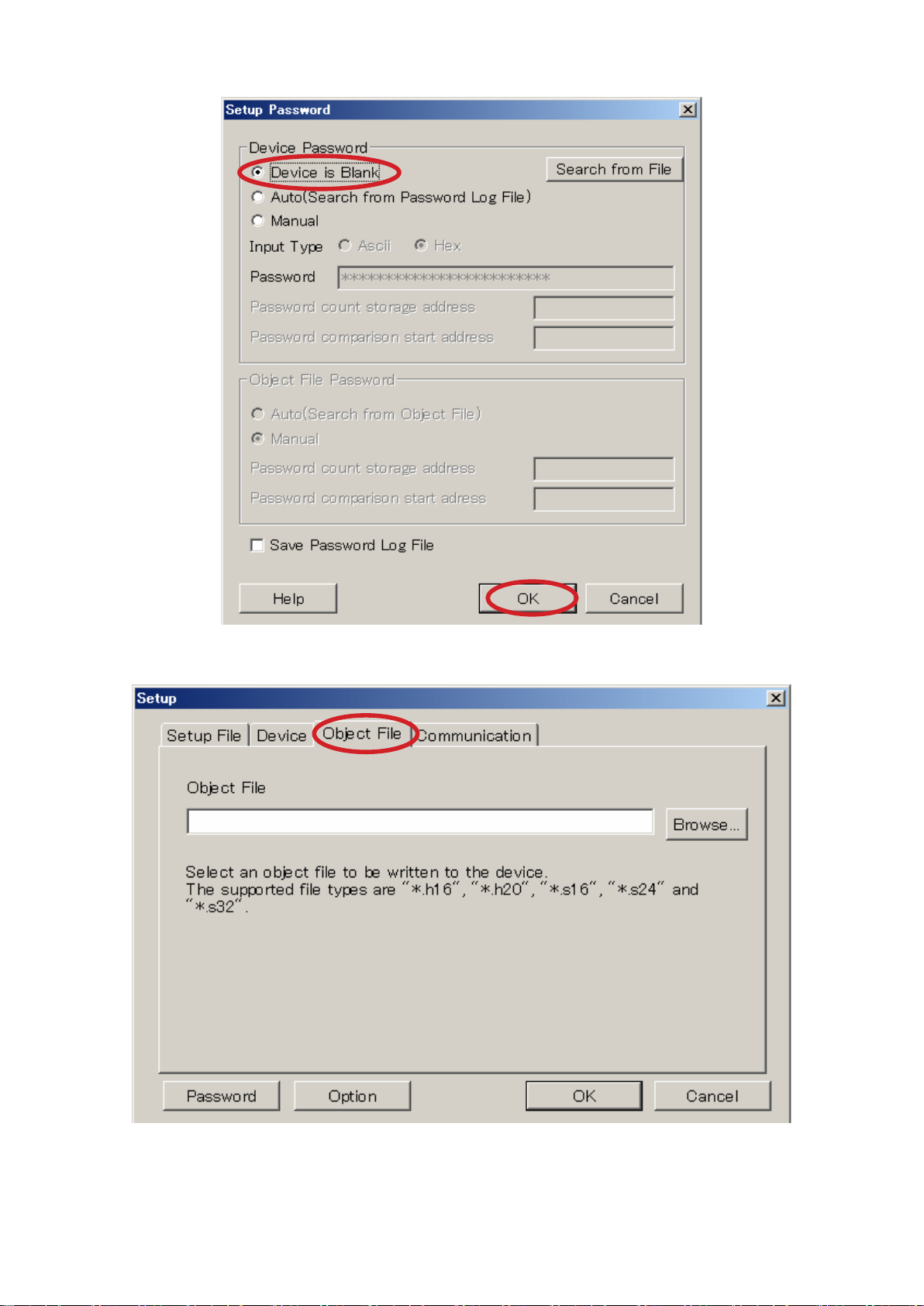
(8) ChoosetheDeviceisBlank.
AndClickOK.
(9) ClickObjectFiletab.
26
Page 27
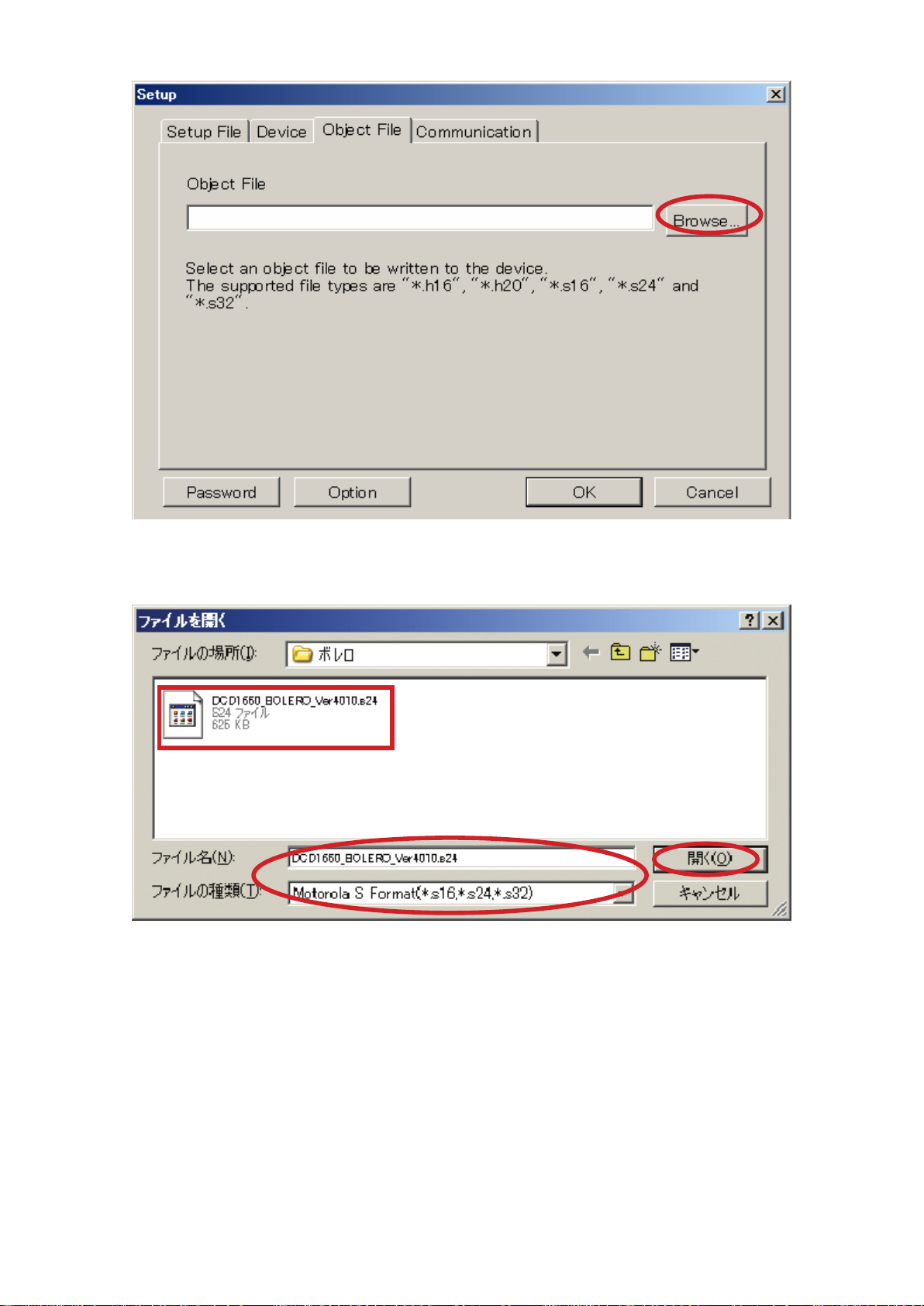
(10)ClickBrowse.
(11)ChoosetheMotorolaSFormat(*.s16,*.s24,*.s32)inFilesoftype.
ChoosetheDCD1650_BOLERO_Ver0_4010.s24,andclickOpen.
27
Page 28
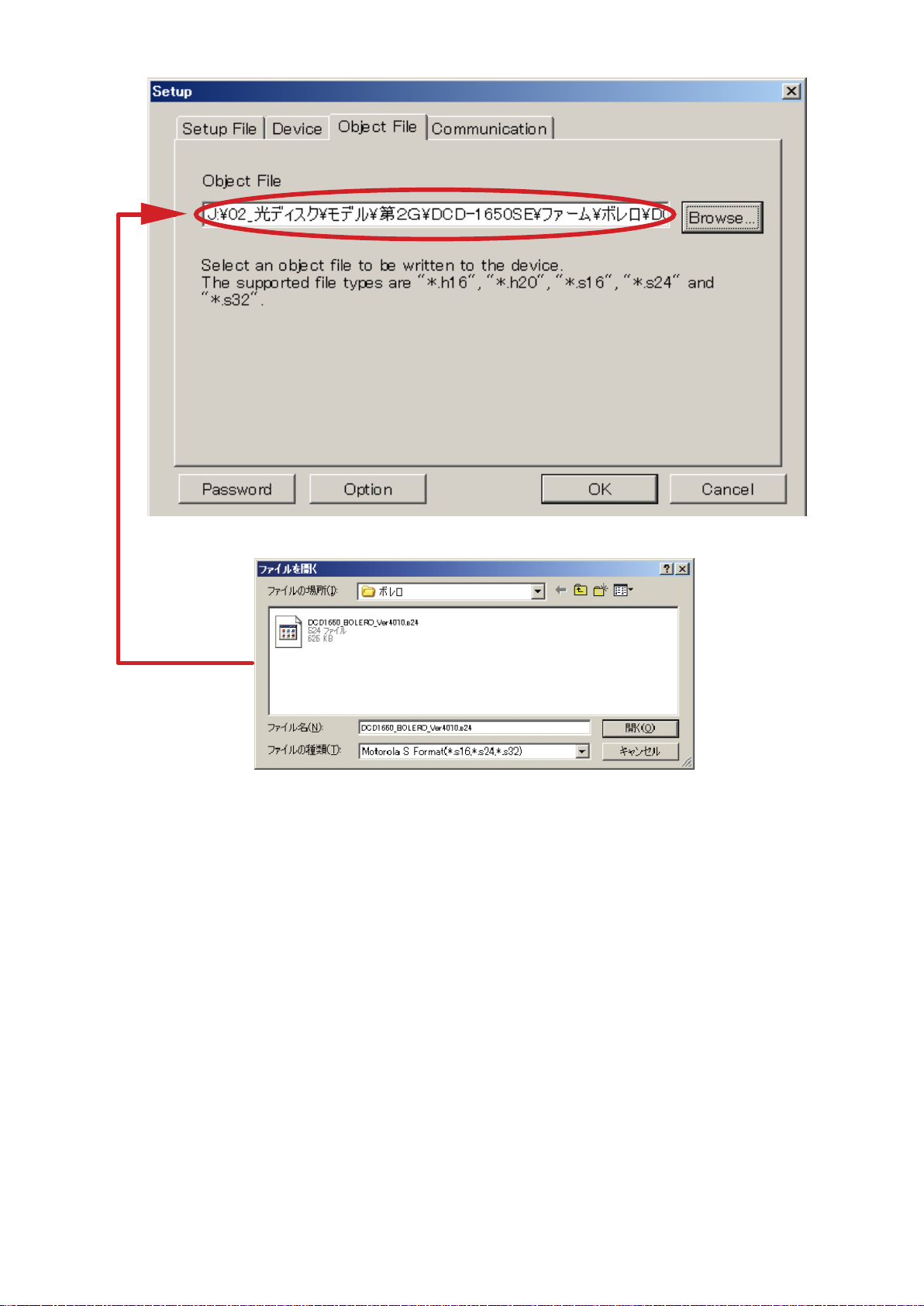
(12)Theplaceoftheleisdisplayed.
28
Page 29
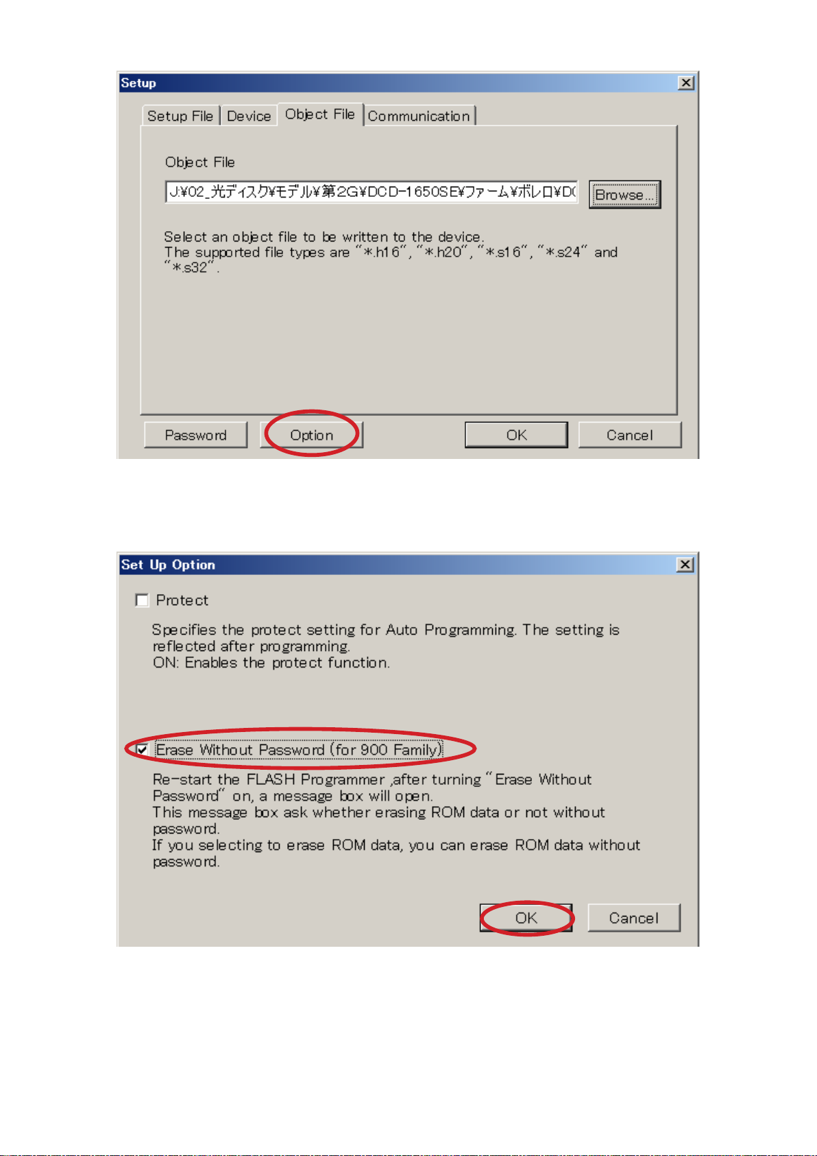
(13)ClickOption.
(14)ChooseEraseWithoutPassword(for900Family).
AndClickOK.
29
Page 30
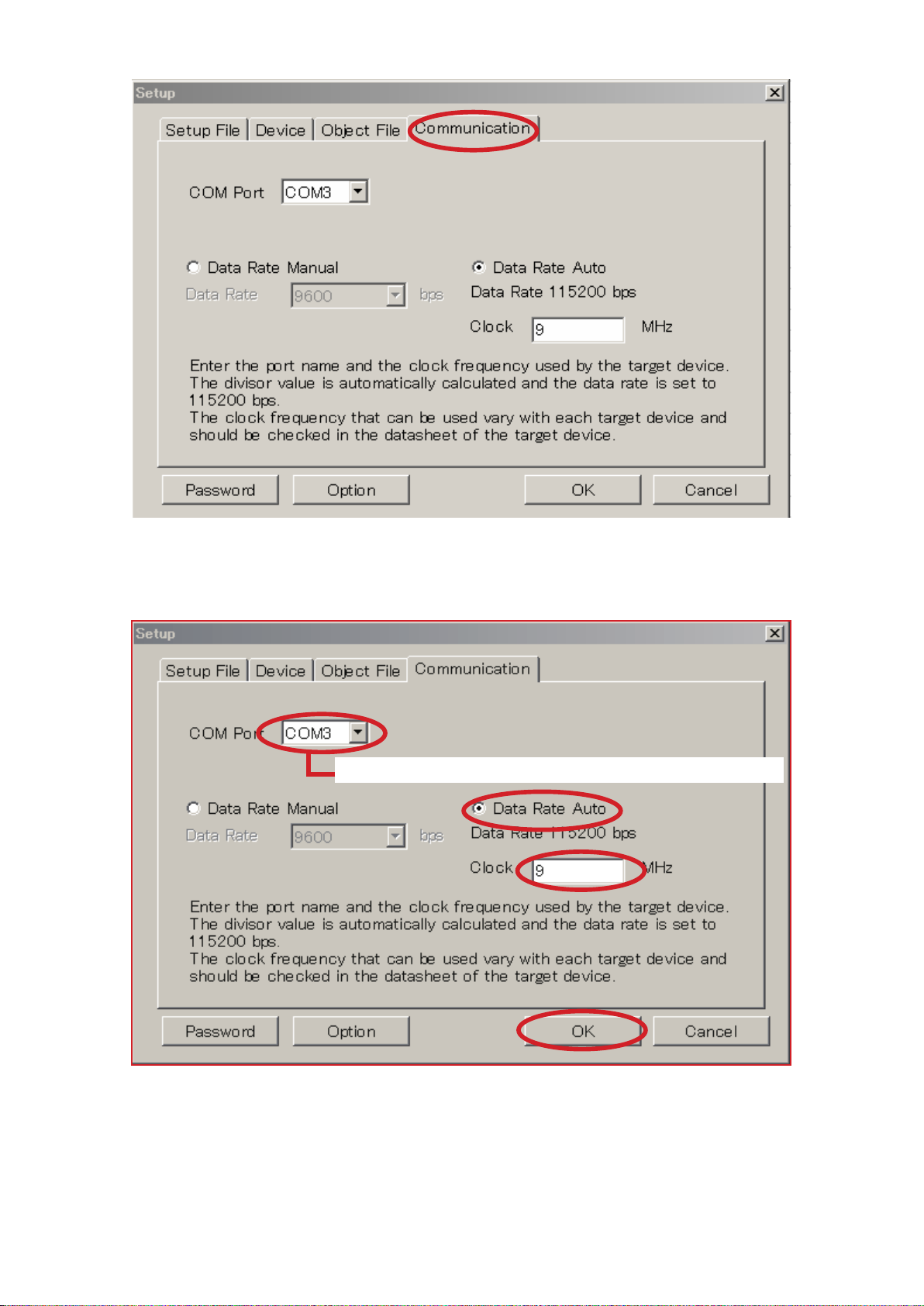
(15)ClickCommunicationtab.
(16)ChoosetheSerialportnumberintheCOMPort.ChecktheDataRateManual,andinput9intheClock.
AndClickOK.
Choose the Serial port that connect with 232C cable.
Thesettingiscompleted.
30
Page 31

(17)TurnonDCD-A100,andpresstheRESETbutton.
PC
①Turn on DCD-2010AE.
(Check connection CY141 on 8U-310040.)
②Press the RESET button.
CX708
(18)IftheconnectionwiththeFlashProgrammerissuccessfullymade,adialogueboxsaying"EraseAlldatainthis
devise?(Y/N)"appearsautomatically.Iftheconnectionfails,errormessagewillappear.(Ex.:E000)
ClickYes.
(19)ClickA(AutoPrograming)tostartwriting.
(20)TurnoffDCD-A100.
(21)RemovetheSPK-581formDCD-A100.
31
Page 32

TROUBLE SHOOTING
8U-210083-1(DIGITAL POWER UNIT)
㪚㪿㪼㪺㫂㩷㫋㪿㪼㩷㪛㪠㪞㪠㪫㪘㪣㩷㫇㫆㫎㪼㫉㩷㫊㫌㫇㫇㫃㫐㩷㪺㫆㫄㫇㫆㫅㪼㫅㫋㩷
㪚㪿㪼㪺㫂㩷㫋㪿㪼㩷㪺㪸㪹㫃㪼㩷㪸㫅㪻㩷㫋㪿㪼㩷㪺㫆㫅㫅㪼㪺㫋㫀㫆㫅㩷㫆㪽㩷㫋㪿㪼㩷㪺㫆㫅㫅㪼㪺㫋㫆㫉㪅
㪚㪿㪼㪺㫂㩷㪪㫆㫃㪻㪼㫉㫀㫅㪾㪅
䇭䊶㪪㪫㪘㪥㪛㪙㪰㩷㪫㪩㪘㪥㪪㪃㪛㪏㪈㪊㪃㪛㪏㪈㪋㪃㪛㪏㪈㪎㪃㪛㪏㪈㪏
䇭䊶㪠㪚㪏㪇㪊㪃㪚㪯㪇㪊㪈㪃㪚㪯㪇㪊㪋
䇭䊶㪚㪰㪇㪊㪋㪃㪪㪏㪇㪈䋺㪏㪬㪄㪉㪈㪇㪇㪏㪊㪄㪋
㪚㪿㪼㪺㫂㩷㪪㫆㫃㪻㪼㫉㫀㫅㪾㪅
䇭䊶㪛㪏㪉㪇㪃㪛㪏㪉㪈㪃㪫㪩㪏㪇㪉㪃㪫㪩㪏㪇㪊
㪚㪿㪼㪺㫂㩷㫋㪿㪼㩷㪺㪸㪹㫃㪼㩷㪸㫅㪻㩷㫋㪿㪼㩷㪺㫆㫅㫅㪼㪺㫋㫀㫆㫅㩷㫆㪽㩷㫋㪿㪼㩷㪺㫆㫅㫅㪼㪺㫋㫆㫉㪅
㪚㪿㪼㪺㫂㩷㪪㫆㫃㪻㪼㫉㫀㫅㪾㪅
䇭䊶㪚㪯㪈㪋㪈
䇭䊶㪚㪰㪈㪋㪈㩷㪑㪏㪬㪄㪊㪈㪇㪇㪋㪇
䇭䊶㪠㪚㪌㪇㪉㪃㪠㪚㪌㪇㪊㪃㪯㪌㪇㪈㪃㪠㪚㪌㪇㪍㩷㪑㪏㪬㪄㪊㪈㪇㪇㪋㪇
㪚㪿㪼㪺㫂㩷㫋㪿㪼㩷㪺㪸㪹㫃㪼㩷㪸㫅㪻㩷㫋㪿㪼㩷㪺㫆㫅㫅㪼㪺㫋㫀㫆㫅㩷㫆㪽㩷㫋㪿㪼㩷㪺㫆㫅㫅㪼㪺㫋㫆㫉㪅
㪚㪿㪼㪺㫂㩷㪪㫆㫃㪻㪼㫉㫀㫅㪾㪅
䇭䊶㪛㪠㪞㪠㪫㪘㪣㩷㪫㪩㪘㪥㪪
䇭䊶㪚㪯㪇㪊㪊㪃㪚㪯㪇㪏㪈㪃㪫㪩㪏㪇㪌㪃㪩㪏㪊㪏㪃㪩㪣㪐㪇㪈
㪚㪿㪼㪺㫂㩷㫋㪿㪼㩷㫊㪼㪺㫆㫅㪻㪸㫉㫐㩷㫉㪼㪺㫋㫀㪽㫀㪺㪸㫋㫀㫆㫅㩷㪺㫀㫉㪺㫌㫀㫋㩷㪸㫅㪻㩷㫋㪿㪼㩷㫊㫆㫃㪻㪼㫉
㫆㪽㩷㫋㪿㪼㩷㫉㪼㪾㫌㫃㪸㫋㫆㫉㪅
䇭䊶㪛㪏㪉㪌㪃㪛㪏㪊㪇㪃㪛㪏㪊㪈
䇭䊶㪠㪚㪏㪇㪈㪃㪏㪇㪉㪃㪠㪚㪏㪇㪌㪃㪠㪚㪏㪇㪍㪃㪠㪚㪏㪇㪎
㪚㪿㪼㪺㫂㩷㫋㪿㪼㩷㪺㪸㪹㫃㪼㩷㪸㫅㪻㩷㫋㪿㪼㩷㪺㫆㫅㫅㪼㪺㫋㫀㫆㫅㩷㫆㪽㩷㫋㪿㪼㩷㪺㫆㫅㫅㪼㪺㫋㫆㫉㪅
㪚㪿㪼㪺㫂㩷㪪㫆㫃㪻㪼㫉㫀㫅㪾㪅
䇭䊶㪚㪯㪈㪋㪈
䇭䊶㪚㪰㪈㪋㪈㩷㪑㪏㪬㪄㪊㪈㪇㪇㪋㪇
䇭䊶㪠㪚㪏㪇㪌㪃㪛㪏㪇㪊㪃㪣㪏㪇㪌
㪚㪿㪼㪺㫂㩷㫋㪿㪼㩷㪺㪸㪹㫃㪼㩷㪸㫅㪻㩷㫋㪿㪼㩷㪺㫆㫅㫅㪼㪺㫋㫀㫆㫅㩷㫆㪽㩷㫋㪿㪼㩷㪺㫆㫅㫅㪼㪺㫋㫆㫉㪅
㪚㪿㪼㪺㫂㩷㪪㫆㫃㪻㪼㫉㫀㫅㪾㪅
䇭䊶㪚㪯㪈㪋㪈
䇭䊶㪚㪰㪈㪋㪈㩷㪑㪏㪬㪄㪊㪈㪇㪇㪋㪇
䇭䊶㪠㪚㪏㪇㪎㪃㪛㪏㪇㪌㪃㪣㪏㪇㪍
㪚㪿㪼㪺㫂㩷㫋㪿㪼㩷㪺㪸㪹㫃㪼㩷㪸㫅㪻㩷㫋㪿㪼㩷㪺㫆㫅㫅㪼㪺㫋㫀㫆㫅㩷㫆㪽㩷㫋㪿㪼㩷㪺㫆㫅㫅㪼㪺㫋㫆㫉㪅
㪚㪿㪼㪺㫂㩷㪪㫆㫃㪻㪼㫉㫀㫅㪾㪅
䇭䊶㪚㪯㪈㪋㪈
䇭䊶㪚㪰㪈㪋㪈㩷㪑㪏㪬㪄㪊㪈㪇㪇㪋㪇
䇭䊶㪠㪚㪏㪇㪍㪃㪛㪏㪇㪋㪃㪣㪏㪇㪋
㪚㪿㪼㪺㫂㩷㫋㪿㪼㩷㪺㪸㪹㫃㪼㩷㪸㫅㪻㩷㫋㪿㪼㩷㪺㫆㫅㫅㪼㪺㫋㫀㫆㫅㩷㫆㪽㩷㫋㪿㪼㩷㪺㫆㫅㫅㪼㪺㫋㫆㫉㪅
㪚㪿㪼㪺㫂㩷㪪㫆㫃㪻㪼㫉㫀㫅㪾㪅
䇭䊶㪚㪯㪈㪋㪈
䇭䊶㪚㪰㪈㪋㪈㩷㪑㪏㪬㪄㪊㪈㪇㪇㪋㪇
䇭䊶㪠㪚㪏㪇㪈㪃㪠㪚㪏㪇㪉㪃㪠㪚㪏㪇㪏
㪚㪿㪼㪺㫂㩷㫋㪿㪼㩷㪺㪸㪹㫃㪼㩷㪸㫅㪻㩷㫋㪿㪼㩷㪺㫆㫅㫅㪼㪺㫋㫀㫆㫅㩷㫆㪽㩷㫋㪿㪼㩷㪺㫆㫅㫅㪼㪺㫋㫆㫉㪅
㪚㪿㪼㪺㫂㩷㪪㫆㫃㪻㪼㫉㫀㫅㪾㪅
䇭䊶㪚㪯㪇㪎㪈
䇭䊶㪚㪰㪇㪎㪈㩷㪑㩷㪏㪬㪄㪉㪈㪇㪇㪏㪊㪄㪉
䇭䊶㪫㪩㪏㪇㪈㪃㪱㪛㪏㪇㪉㪃㪱㪛㪏㪇㪊㪃㪠㪚㪏㪇㪋
㪚㪿㪼㪺㫂㩷㪧㫆㫎㪼㫉㩷㪪㫌㫇㫇㫃㫐㪄㪈
㪏㪬㪄㪉㪈㪇㪇㪏㪊㪄㪈㩿㪛㪠㪞㪠㪫㪘㪣㩷㪧㪦㪮㪜㪩㩷㪬㪥㪠㪫㪀
䇭䊶㪚㪿㪼㪺㫂㩷㫋㪿㪼㩷㫆㫌㫋㫇㫌㫋㩷㫍㫆㫃㫋㪸㪾㪼㩷㫆㪽㩷㪚㪯㪈㪋㪈㩷㩿㪈㪈㪀㫇㫀㫅㩷㩷㩷㩷㩷㪂㪊㪅㪊㪭㪶㪥㪪㪮㩷㪑㩷㪊㪅㪊㪭
㪚㪿㪼㪺㫂㩷㪧㫆㫎㪼㫉㩷㪪㫌㫇㫇㫃㫐㪄㪉
㪏㪬㪄㪉㪈㪇㪇㪏㪊㪄㪈㩿㪛㪠㪞㪠㪫㪘㪣㩷㪧㪦㪮㪜㪩㩷㪬㪥㪠㪫㪀
䇭䊶㪚㪿㪼㪺㫂㩷㫋㪿㪼㩷㫆㫌㫋㫇㫌㫋㩷㫍㫆㫃㫋㪸㪾㪼㩷㫆㪽㩷㪚㪯㪈㪋㪈㩷㩿㪈㪉㪀㫇㫀㫅㩷㩷㩷㩷㩷㪧㪅㪛㪦㪮㪥㩷㪑㩷㪊㪅㪊㪭
㪚㪿㪼㪺㫂㩷㪧㫆㫎㪼㫉㩷㪪㫌㫇㫇㫃㫐㪄㪊
㪏㪬㪄㪉㪈㪇㪇㪏㪊㪄㪈㩿㪛㪠㪞㪠㪫㪘㪣㩷㪧㪦㪮㪜㪩㩷㪬㪥㪠㪫㪀
䇭䊶㪚㪿㪼㪺㫂㩷㫋㪿㪼㩷㫆㫌㫋㫇㫌㫋㩷㫍㫆㫃㫋㪸㪾㪼㩷㫆㪽㩷㪚㪯㪈㪋㪈㩷㩿㪈㪊㪀㫇㫀㫅㩷㩷㩷㩷㩷㪧㪶㪚㪦㪥㪫㩷㪑㩷㪊㪅㪊㪭
㪚㪿㪼㪺㫂㩷㪧㫆㫎㪼㫉㩷㪪㫌㫇㫇㫃㫐㪄㪋
㪏㪬㪄㪉㪈㪇㪇㪏㪊㪄㪈㩿㪛㪠㪞㪠㪫㪘㪣㩷㪧㪦㪮㪜㪩㩷㪬㪥㪠㪫㪀
䇭䊶㪚㪿㪼㪺㫂㩷㫋㪿㪼㩷㫆㫌㫋㫇㫌㫋㩷㫍㫆㫃㫋㪸㪾㪼㩷㫆㪽㩷㪚㪯㪇㪏㪈㩷㩿㪊㪀㫇㫀㫅
㪚㪿㪼㪺㫂㩷㪧㫆㫎㪼㫉㩷㪪㫌㫇㫇㫃㫐㪄㪌
㪏㪬㪄㪉㪈㪇㪇㪏㪊㪄㪈㩿㪛㪠㪞㪠㪫㪘㪣㩷㪧㪦㪮㪜㪩㩷㪬㪥㪠㪫㪀
䇭䊶㪚㪿㪼㪺㫂㩷㫋㪿㪼㩷㪝㪬㪪㪜䇭㩿㪝㪏㪇㪈䇮㪝㪏㪇㪉㪃㪝㪏㪇㪊㪀㩷㩷㩷㩷㩷㪚㪿㪼㪺㫂㩷㪝㪬㪪㪜㩷㪚㫆㫅㪻㫀㫋㫀㫆㫅㪅
㪚㪿㪼㪺㫂㩷㪧㫆㫎㪼㫉㩷㪪㫌㫇㫇㫃㫐㪄㪍
㪏㪬㪄㪉㪈㪇㪇㪏㪊㪄㪈㩿㪛㪠㪞㪠㪫㪘㪣㩷㪧㪦㪮㪜㪩㩷㪬㪥㪠㪫㪀
䇭䊶㪚㪿㪼㪺㫂㩷㫋㪿㪼㩷㫆㫌㫋㫇㫌㫋㩷㫍㫆㫃㫋㪸㪾㪼㩷㫆㪽㩷㪚㪯㪈㪋㪈㩷㩿㪈㪇㪀㫇㫀㫅㩷㩷㩷㩷㩷㪂㪊㪅㪊㪭㪶㪛㪌
㪚㪿㪼㪺㫂㩷㪧㫆㫎㪼㫉㩷㪪㫌㫇㫇㫃㫐㪄㪎
㪏㪬㪄㪉㪈㪇㪇㪏㪊㪄㪈㩿㪛㪠㪞㪠㪫㪘㪣㩷㪧㪦㪮㪜㪩㩷㪬㪥㪠㪫㪀
䇭䊶㪚㪿㪼㪺㫂㩷㫋㪿㪼㩷㫆㫌㫋㫇㫌㫋㩷㫍㫆㫃㫋㪸㪾㪼㩷㫆㪽㩷㪚㪯㪈㪋㪈㩷㩿㪍㪀㩿㪎㪀㫇㫀㫅㩷㩷㩷㩷㩷㪂㪊㪅㪊㪭㪶㪛㪈
㪚㪿㪼㪺㫂㩷㪧㫆㫎㪼㫉㩷㪪㫌㫇㫇㫃㫐㪄㪏
㪏㪬㪄㪉㪈㪇㪇㪏㪊㪄㪈㩿㪛㪠㪞㪠㪫㪘㪣㩷㪧㪦㪮㪜㪩㩷㪬㪥㪠㪫㪀
䇭䊶㪚㪿㪼㪺㫂㩷㫋㪿㪼㩷㫆㫌㫋㫇㫌㫋㩷㫍㫆㫃㫋㪸㪾㪼㩷㫆㪽㩷㪚㪯㪈㪋㪈㩷㩿㪈㪀㫇㫀㫅㩷㩷㩷㩷㩷㪂㪌㪭㪶㪬㪪㪙
㪚㪿㪼㪺㫂㩷㪧㫆㫎㪼㫉㩷㪪㫌㫇㫇㫃㫐㪄㪐
㪏㪬㪄㪉㪈㪇㪇㪏㪊㪄㪈㩿㪛㪠㪞㪠㪫㪘㪣㩷㪧㪦㪮㪜㪩㩷㪬㪥㪠㪫㪀
䇭䊶㪚㪿㪼㪺㫂㩷㫋㪿㪼㩷㫆㫌㫋㫇㫌㫋㩷㫍㫆㫃㫋㪸㪾㪼㩷㫆㪽㩷㪚㪯㪈㪋㪈㩷㩿㪉㪀㩿㪊㪀㫇㫀㫅㩷㩷㩷㩷㩷㪂㪌㪭㪶㪤㪈㩷㩷㪑㩷㪌㪭
㩷㩷㩷㩷㩷㩷㩷㩷㩷㩷㩷㩷㩷㩷㩷㩷㩷㩷㩷㩷㩷㩷㩷㩷㩷㩷㩷㩷㩷㩷㩷㩷㩷㩷㩷㩷㩷㩷㩷㩷㩷㩷㩷㩷㩷㩷㩷㩷㩷㩷㩷㩷㩷㩷㩷㩷㩷㩷㩷㩷㩷㩷㩷㩷㩷㩷㩷㩷㪂㪈㪉㪭㪶㪤㪈㪑㩷㪈㪉㪭
㪚㪿㪼㪺㫂㩷㪧㫆㫎㪼㫉㩷㪪㫌㫇㫇㫃㫐㪄㪈㪇
㪏㪬㪄㪉㪈㪇㪇㪏㪊㪄㪈㩿㪛㪠㪞㪠㪫㪘㪣㩷㪧㪦㪮㪜㪩㩷㪬㪥㪠㪫㪀
䇭䊶㪚㪿㪼㪺㫂㩷㫋㪿㪼㩷㫆㫌㫋㫇㫌㫋㩷㫍㫆㫃㫋㪸㪾㪼㩷㫆㪽㩷㪚㪯㪇㪎㪈㩷㩿㪌㪀㩿㪍㪀㩿㪎㪀㫇㫀㫅㩷㩷㩷㩷㩷㩷㩷㪄㪊㪉㪭㪃㪝㪂㪃㪝㪄
䇭䇭䇭䇭䇭䇭䇭䇭䇭䇭䇭䇭䇭䇭䇭䇭䇭䇭䇭䇭䇭䇭䇭䇭䇭䇭㩿㪧㫆㫎㪼㫉㩷㫊㫌㫇㫇㫃㫐㩷㪽㫆㫉㩷㪝㪣㩷㪛㫀㫊㫇㫃㪸㫐㪀
㪥㪅㪞㪅
㪥㪅㪞㪅
㪥㪅㪞㪅
㪥㪅㪞㪅
㪥㪅㪞㪅
㪥㪅㪞㪅
㪥㪅㪞㪅
㪥㪅㪞㪅
㪥㪅㪞㪅
㪥㪅㪞㪅
㪦㪅㪢㪅
㪦㪅㪢㪅
㪦㪅㪢㪅
㪦㪅㪢㪅
㪦㪅㪢㪅
㪦㪅㪢㪅
㪦㪅㪢㪅
㪦㪅㪢㪅
㪦㪅㪢㪅
㪜㪥㪛
㪦㪅㪢㪅
32
Page 33

8U-310040(SACD MODULE UNIT-FE/BE BLOCK)
㪚㪿㪼㪺㫂㩷㫋㪿㪼㩷㪝㪜㪆㪙㪜㩷㪺㫆㫄㫇㫆㫅㪼㫅㫋
㪈㪅㪈㪚㪿㪼㪺㫂㩷㫋㪿㪼㩷㫇㫆㫎㪼㫉㩷㫊㫌㫇㫇㫃㫐
㪈㪅㪉㪛㫆㪼㫊㩷㫅㫆㫋㩷㪩㪼㪸㪻㩷㪛㫀㫊㪺
䇭㩿㪈㪀㪛㫀㫊㪺㩷㪻㫆㪼㫊㩷㫅㫆㫋㩷㪩㫆㫋㪸㫋㪼㪅
㪚㪿㪼㪺㫂㩷㪧㫆㫎㪼㫉㩷㪪㫌㫇㫇㫃㫐㪄㪈
㪏㪬㪄㪊㪈㪇㪇㪋㪇㩿㪪㪘㪚㪛㩷㪤㪦㪛㪬㪣㪜㩷㪬㪥㪠㪫㪀
䇭䊶㪚㪿㪼㪺㫂㩷㫋㪿㪼㩷㫆㫌㫋㫇㫌㫋㩷㫍㫆㫃㫋㪸㪾㪼㩷㫆㪽㩷㪚㪰㪈㪋㪈㩷㩿㪊㪀㫇㫀㫅㩷㩷㩷㩷㩷㪂㪌㪭㪶㪛㪈㩷㪑㩷㪌㪭
㪚㪿㪼㪺㫂㩷㫋㪿㪼㩷㪺㪸㪹㫃㪼㩷㪸㫅㪻㩷㫋㪿㪼㩷㪺㫆㫅㫅㪼㪺㫋㫀㫆㫅㩷㫆㪽㩷㫋㪿㪼㩷㪺㫆㫅㫅㪼㪺㫋㫆㫉㪅
㪚㪿㪼㪺㫂㩷㪪㫆㫃㪻㪼㫉㫀㫅㪾
䇭䊶㪚㪰㪈㪋㪈
䇭䊶㪠㪚㪏㪇㪈㩷㪑㩷㪏㪬㪄㪉㪈㪇㪇㪏㪊㪄㪈
㪸㫅㪻㩷㪦㫋㪿㪼㫉㩷㪚㫀㫉㪺㫌㫀㫋㫊
㪚㪿㪼㪺㫂㩷㪧㫆㫎㪼㫉㩷㪪㫌㫇㫇㫃㫐㪄㪉
㪏㪬㪄㪊㪈㪇㪇㪋㪇㩿㪪㪘㪚㪛㩷㪤㪦㪛㪬㪣㪜㩷㪬㪥㪠㪫㪀
䇭䊶㪚㪿㪼㪺㫂㩷㫋㪿㪼㩷㫆㫌㫋㫇㫌㫋㩷㫍㫆㫃㫋㪸㪾㪼㩷㫆㪽㩷㪚㪰㪈㪋㪈㩷㩿㪍㪀㩿㪎㪀㫇㫀㫅㩷㩷㩷㩷㩷㪂㪊㪅㪊䌖㪶㪛㪈㩷㪑㩷㪊㪅㪊㪭
㪚㪿㪼㪺㫂㩷㫋㪿㪼㩷㪺㪸㪹㫃㪼㩷㪸㫅㪻㩷㫋㪿㪼㩷㪺㫆㫅㫅㪼㪺㫋㫀㫆㫅㩷㫆㪽㩷㫋㪿㪼㩷㪺㫆㫅㫅㪼㪺㫋㫆㫉㪅
㪚㪿㪼㪺㫂㩷㪪㫆㫃㪻㪼㫉㫀㫅㪾
䇭䊶㪚㪰㪈㪋㪈
䇭䊶㪠㪚㪏㪇㪎㩷㪑㩷㪏㪬㪄㪉㪈㪇㪇㪏㪊㪄㪈
㪸㫅㪻㩷㪦㫋㪿㪼㫉㩷㪚㫀㫉㪺㫌㫀㫋㫊
㪚㪿㪼㪺㫂㩷㪧㫆㫎㪼㫉㩷㪪㫌㫇㫇㫃㫐㪄㪊
㪏㪬㪄㪊㪈㪇㪇㪋㪇㩿㪪㪘㪚㪛㩷㪤㪦㪛㪬㪣㪜㩷㪬㪥㪠㪫㪀
䇭䊶㪚㪿㪼㪺㫂㩷㫋㪿㪼㩷㫆㫌㫋㫇㫌㫋㩷㫍㫆㫃㫋㪸㪾㪼㩷㫆㪽㩷㪠㪚㪌㪇㪈㩷㩷㩷㩷㩷㩷㪂㪉㪅㪌㪶㪛㪈㪆㪶㪘㪈㩷㪑㩷㪉㪅㪌㪭
㪚㪿㪼㪺㫂㩷㫋㪿㪼㩷㪺㪸㪹㫃㪼㩷㪸㫅㪻㩷㫋㪿㪼㩷㪺㫆㫅㫅㪼㪺㫋㫀㫆㫅㩷㫆㪽㩷㫋㪿㪼㩷㪺㫆㫅㫅㪼㪺㫋㫆㫉㪅
㪚㪿㪼㪺㫂㩷㪪㫆㫃㪻㪼㫉㫀㫅㪾
䇭䊶㪚㪰㪈㪋㪈㪃㪠㪚㪌㪇㪈
㪸㫅㪻㩷㪦㫋㪿㪼㫉㩷㪚㫀㫉㪺㫌㫀㫋㫊
㪦㪅㪢㪅
㪦㪅㪢㪅
㪦㪅㪢㪅
㪥㪅㪞㪅
㪚㪿㪼㪺㫂㩷㫋㪿㪼㩷㪜㫄㫀㫊㫊㫀㫆㫅㩷㫆㪽㩷㪧㫀㪺㫂㪄㫌㫇㪅
㪏㪬㪄㪊㪈㪇㪇㪋㪇㩿㪪㪘㪚㪛㩷㪤㪦㪛㪬㪣㪜㩷㪬㪥㪠㪫㪀
䇭䊶㪜㫄㫀㫊㫊㫀㫆㫅㩷㫆㪽㩷㪧㪅㪬㪅㩷㫃㪸㫊㪼㫉㩷㪦㪅㪢㪅㪖
䇭䊶㪫㪿㪼㩷㫋㪼㫊㫋㩷㫄㫆㪻㪼㩷㩹㪫㪉㩹㩷㫀㫊㩷㪼㫏㪼㪺㫌㫋㪼㪻㪅
㩷㩷䇭㪣㪸㫊㪼㫉㩷㪺㫌㫉㫉㪼㫅㫋㩷㪦㪅㪢㪅㪖
㩿㪈㪀䇭㪚㪿㪼㪺㫂㩷㫋㪿㪼㩷㫃㪸㫊㪼㫉㩷㫊㫆㫃㪻㪼㫉㩷㫊㪿㫆㫉㫋㩷㫃㪸㫅㪻㩷㫆㪽㩷㪧㪅㪬㩷㪸㫅㪻
㩷㩷㩷㩷㩷㩷㪏㪬㪄㪊㪈㪇㪇㪋㪇㪅
㩿㪉㪀䇭㪚㪿㪼㪺㫂㩷㫋㪿㪼㩷㪺㫀㫉㪺㫌㫄㪽㪼㫉㪼㫅㪺㪼㩷㫊㫆㫃㪻㪼㫉㫀㫅㪾㩷㫆㪽㩷㪲㪫㪩㪈㪇㪈㪴
㩷㩷㩷㩷㩷㩷㩷㪸㫅㪻㩷㪲㪫㪩㪈㪇㪌㪴㪅
㩿㪊㪀䇭㪚㪿㪼㪺㫂㩷㪺㫆㫅㫅㪼㪺㫋㫆㫉㩷㫀㫅㫊㪼㫉㫋㫀㫆㫅㪅䊶䊶䊶㪧㪅㪬㪅㪄㪚㪯㪉㪋㪈
㩿㪋㪀䇭㪚㪿㪼㪺㫂㩷㫋㪿㪼㩷㫊㫆㫃㪻㪼㫉㫀㫅㪾㩷㪲㪠㪚㪈㪇㪈㪴㩷㪸㫅㪻㩷㪺㫀㫉㪺㫌㫄㪽㪼㫉㪼㫅㪺㪼
㩷㩷㩷㩷㩷㩷㫊㫆㫃㪻㪼㫉㫀㫅㪾㩷㫆㪽㩷㪲㪠㪚㪈㪇㪈㪴
㩿㪌㪀䇭㪚㪿㪼㪺㫂㩷㫋㪿㪼㩷㫊㫆㫃㪻㪼㫉㫀㫅㪾㩷㪲㪠㪚㪈㪇㪎㪴㩷㪸㫅㪻㩷㪺㫀㫉㪺㫌㫄㪽㪼㫉㪼㫅㪺㪼
㩷㩷㩷㩷㩷㩷㫊㫆㫃㪻㪼㫉㫀㫅㪾㩷㫆㪽㩷㪲㪠㪚㪈㪇㪎㪴
㪚㪿㪼㪺㫂㩷㫋㪿㪼㩷㫊㫇㫀㫅㪻㫃㪼㩷㪻㫉㫀㫍㪼㩷㫊㫀㪾㫅㪸㫃㪅
㪏㪬㪄㪊㪈㪇㪇㪋㪇㩿㪪㪘㪚㪛㩷㪤㪦㪛㪬㪣㪜㩷㪬㪥㪠㪫㪀
䇭䊶㪲㪪㪧㪠㪥㪛㪣㪜㪴䋺㩹㪟㩹㫃㪼㫍㪼㫃䋿
㩿㪈㪀䇭㪚㪿㪼㪺㫂㩷㫊㫆㫃㪻㪼㫉㫀㫅㪾㩷㫆㪽㩷㪲㪠㪚㪈㪇㪎㪴㪑㪏㪌㪃㩷㪐㪇㫇㫀㫅
㩿㪉㪀䇭㪚㪿㪼㪺㫂㩷㫋㪿㪼㩷㪺㫀㫉㪺㫌㫄㪽㪼㫉㪼㫅㪺㪼㩷㫊㫆㫃㪻㪼㫉㫀㫅㪾㩷㫆㪽㩷㪲㪪㪧㪠㪥㪛㪣㪜㪴㪃
㩷㩷㩷㩷㩷㩷㪲㪝㪞㪠㪥㪴㩷㫊㫀㪾㫅㪸㫃㪅
㩿㪊㪀䇭㪚㪿㪼㪺㫂㩷㫋㪿㪼㩷㪺㫆㫅㫅㪼㪺㫋㫆㫉㩷㪺㫆㫅㫅㪼㪺㫋㫀㫆㫅㪅䊶䊶䊶㪤㪼㪺㪿㪸㪄㪚㪯㪈㪌㪈
㩿㪋㪀䇭㪚㪿㪼㪺㫂㩷㫋㪿㪼㩷㫊㫆㫃㪻㪼㫉㫀㫅㪾㩷㪲㪠㪚㪈㪇㪈㪴㩷㪸㫅㪻㩷㪺㫀㫉㪺㫌㫄㪽㪼㫉㪼㫅㪺㪼
㩷㩷㩷㩷㩷㩷㫊㫆㫃㪻㪼㫉㫀㫅㪾㩷㫆㪽㩷㪲㪠㪚㪈㪇㪈㪴
㪦㪅㪢㪅
㪦㪅㪢㪅
㪚㪿㪼㪺㫂㩷㪧㫆㫎㪼㫉㩷㪪㫌㫇㫇㫃㫐㪄㪊
㪏㪬㪄㪊㪈㪇㪇㪋㪇㩿㪪㪘㪚㪛㩷㪤㪦㪛㪬㪣㪜㩷㪬㪥㪠㪫㪀
䇭䊶㪚㪿㪼㪺㫂㩷㫋㪿㪼㩷㫆㫌㫋㫇㫌㫋㩷㫍㫆㫃㫋㪸㪾㪼㩷㫆㪽㩷㪠㪚㪈㪇㪋㩷㩷㩷㩷㩷㪂㪈㪅㪉㪶㪛㪭㪊㪅㪉㩷㪑㩷㪈㪅㪉㪭
㪚㪿㪼㪺㫂㩷㫋㪿㪼㩷㪺㪸㪹㫃㪼㩷㪸㫅㪻㩷㫋㪿㪼㩷㪺㫆㫅㫅㪼㪺㫋㫀㫆㫅㩷㫆㪽㩷㫋㪿㪼㩷㪺㫆㫅㫅㪼㪺㫋㫆㫉㪅
㪚㪿㪼㪺㫂㩷㪪㫆㫃㪻㪼㫉㫀㫅㪾
䇭䊶㪚㪰㪈㪋㪈㪃㪠㪚㪈㪇㪋
㪸㫅㪻㩷㪦㫋㪿㪼㫉㩷㪚㫀㫉㪺㫌㫀㫋㫊
㪦㪅㪢㪅
㪥㪅㪞㪅
㪥㪅㪞㪅
㪥㪅㪞㪅
㪥㪅㪞㪅
㪥㪅㪞㪅
㪜㪥㪛
㪜㪥㪛
33
Page 34

䇭㩿㪉㪀㪚㪛㩷㫆㫉㩷㪪㪘㪚㪛㩿㪛㪭㪛㪀㩷㪺㪿㪼㪺㫂㩷㫇㫉㫆㪺㪼㫊㫊
䇭㩿㪊㪀㩷㪪㪘㪚㪛㩷㪺㪿㪼㪺㫂㩷㫇㫉㫆㪺㪼㫊㫊
㪈㪌㪇
㪚㪿㪼㪺㫂㩷㫋㪿㪼㩷㪩㪝㩷㫊㫀㪾㫅㪸㫃㪅
㪏㪬㪄㪊㪈㪇㪇㪋㪇㩿㪪㪘㪚㪛㩷㪤㪦㪛㪬㪣㪜㩷㪬㪥㪠㪫㪀
䇭䊶㪚㪿㪼㪺㫂㩷㫋㪿㪼㩷㫍㫆㫃㫋㪸㪾㪼㩷㫆㪽㩷㪫㪼㫊㫋㪄㪧㫆㫀㫅㫋㩷㩿㪫㪧㪀㪀
䇭䊶㪫㪧㪲㫄㪘㪤㪦㪥㪈㪴㩷㪲㪘㪤㪦㪥㪉㪴㪑㩷㪻㫀㪽㪽㪼㫉㪼㫅㫋㫀㪸㫃㩷㫆㫌㫋㫇㫌㫋㩷㪸㪹㫆㫌㫋㩷㪎㪇㪇㫄㪭㫇㪄㫇
㪚㪿㪼㪺㫂㩷㪪㫆㫃㪻㪼㫉㫀㫅㪾
㪏㪬㪄㪊㪈㪇㪇㪋㪇㩿㪪㪘㪚㪛㩷㪤㪦㪛㪬㪣㪜㩷㪬㪥㪠㪫㪀
䇭䊶㪚㪿㪼㪺㫂㩷㫋㪿㪼㩷㫊㫆㫃㪻㪼㫉㫀㫅㪾㩷㪲㪠㪚㪈㪇㪎㪴㩷㪸㫅㪻㩷㪺㫀㫉㪺㫌㫄㪽㪼㫉㪼㫅㪺㪼
㩷㩷㩷㩷㫊㫆㫃㪻㪼㫉㫀㫅㪾㩷㫆㪽㩷㪲㪠㪚㪈㪇㪎㪴
㪦㪅㪢㪅
㪚㪿㪼㪺㫂㩷㪧㫆㫎㪼㫉㩷㪪㫌㫇㫇㫃㫐
㪏㪬㪄㪊㪈㪇㪇㪋㪇㩿㪪㪘㪚㪛㩷㪤㪦㪛㪬㪣㪜㩷㪬㪥㪠㪫㪀
䇭䊶㪚㪿㪼㪺㫂㩷㫋㪿㪼㩷㪠㪚㪊㪇㪊㩷㫇㫆㫎㪼㫉㩷㫊㫌㫇㫇㫃㫐㩷㫍㫆㫃㫋㪸㪾㪼㪅㩷㩷㩷㩷㩷㪂㪊㪅㪊㪭㪶㪛㪈㩷㩷㪑㩷㪊㪅㪊䌖
䇭䇭䇭䇭䇭䇭䇭䇭䇭䇭䇭䇭䇭䇭䇭䇭䇭䇭䇭䇭䇭䇭䇭䇭䇭㩷㩷㩷䇭㪂㪉㪅㪌㪶㪛㪈㪆㪶㪘㪈㩷㪑㩷㪉㪅㪌㪭
㪚㪿㪼㪺㫂㩷㫋㪿㪼㩷㪺㪸㪹㫃㪼㩷㪸㫅㪻㩷㫋㪿㪼㩷㪺㫆㫅㫅㪼㪺㫋㫀㫆㫅㩷㫆㪽㩷㫋㪿㪼㩷㪺㫆㫅㫅㪼㪺㫋㫆㫉㪅
㪚㪿㪼㪺㫂㩷㪪㫆㫃㪻㪼㫉㫀㫅㪾
䇭䊶㪚㪰㪈㪋㪈㪃㪠㪚㪌㪇㪈
䇭䊶㪚㪯㪈㪋㪈㩷㪑㪏㪬㪄㪉㪈㪇㪇㪏㪊
㪚㪿㪼㪺㫂㩷㪦㫊㪺㫀㫃㫃㪸㫋㫀㫆㫅㩷㫎㪸㫍㪼㪽㫆㫉㫄㪅
㪏㪬㪄㪊㪈㪇㪇㪋㪇㩿㪪㪘㪚㪛㩷㪤㪦㪛㪬㪣㪜㩷㪬㪥㪠㪫㪀
䇭䊶㪠㪚㪊㪇㪊㩷㩿㪈㪈㪀㫇㫀㫅㩷㩷㩷㩷㩷㩷㩷㩷㩷㩷㩷㩷㩷㩷㩷㩷㩷㩷㩷㩷㩷㩷㪤㪚㪢㪈㩷㪑㩷㪊㪊㪅㪏㪎㪤㪟㫑㩷㩿㪊㪅㪊㪭㪀
㪚㪿㪼㪺㫂㩷㫋㪿㪼㩷㪺㪸㪹㫃㪼㩷㪸㫅㪻㩷㫋㪿㪼㩷㪺㫆㫅㫅㪼㪺㫋㫀㫆㫅㩷㫆㪽㩷㫋㪿㪼㩷㪺㫆㫅㫅㪼㪺㫋㫆㫉㪅
㪚㪿㪼㪺㫂㩷㪪㫆㫃㪻㪼㫉㫀㫅㪾
䇭䊶㪠㪚㪊㪇㪊㪃㪩㪊㪉㪇㪃㪩㪍㪇㪊㪃㪠㪚㪌㪈㪇㪃㪚㪯㪉㪈㪈
䇭䊶㪚㪰㪉㪈㪈㪃㪠㪚㪈㪇㪋㩷㪑㩷㪏㪬㪄㪉㪈㪇㪇㪏㪊㪄㪎
㪚㪿㪼㪺㫂㩷㪩㪼㫊㪼㫋㩷㫊㫀㪾㫅㪸㫃㪅
㪏㪬㪄㪊㪈㪇㪇㪋㪇㩿㪪㪘㪚㪛㩷㪤㪦㪛㪬㪣㪜㩷㪬㪥㪠㪫㪀
䇭䊶㪠㪚㪊㪇㪊㩷㩿㪐㪀㫇㫀㫅㩷㩷㩷㩷㩷㩷㩷㩷㩷㩷㩷㩷㩷㩷㩷㩷㩷㩷㩷㩷㩷㩷㪠㪦㪶㪩㪪㪫㩷㪑㩷㩹㪟㩹㩷㫃㪼㫍㪼㫃㩷㩿㪊㪅㪊㪭㪀
㪚㪿㪼㪺㫂㩷㪪㫆㫃㪻㪼㫉㫀㫅㪾
䇭䊶㪩㪊㪈㪏㪃㪩㪉㪊㪌㪃㪠㪚㪈㪇㪎
㪚㪿㪼㪺㫂㩷㪙㫌㫊㩷㪣㫀㫅㪼㪅
㪏㪬㪄㪊㪈㪇㪇㪋㪇㩿㪪㪘㪚㪛㩷㪤㪦㪛㪬㪣㪜㩷㪬㪥㪠㪫㪀
䇭䊶㪚㪿㪼㪺㫂㩷㪘㪻㪻㫉㪼㫊㫊㪃㩷㪛㪸㫋㪸㩷㪙㫌㫊㩷㪹㪼㫋㫎㪼㪼㫅㩷㪠㪚㪊㪇㪊㩷㪸㫅㪻㩷㪠㪚㪊㪇㪈㩿㪪㪛㪩㪘㪤㪀
䇭㩹㪟㩹㹤㩹㪣㩹㩷㫊㫎㫀㫋㪺㪿㫀㫅㪾
㪚㪿㪼㪺㫂㩷㪪㫆㫃㪻㪼㫉㫀㫅㪾
䇭䊶㪘㪻㪻㫉㪼㫊㫊㪃㩷㪛㪸㫋㪸㪃㩷㪚㫆㫅㫋㫉㫆㫃㩷㪪㫀㪾㫅㪸㫃㪅
䇭䊶㪲㪛㪨㪇㪄㪎㪴㪃㪲㪛㪶㪤㪘㪇㪄㪈㪈㪴㪃㪲㪛㪚㪣㪢㪴㪃㪲㪛㪚㪢㪜㪴㪃㪲㪛㪮㪜㪴㪃
㩷㩷㩷㩷㪲㪥㪚㪘㪪㪴㪃㪲㪥㪩㪘㪪㪴
㪦㪅㪢㪅
㪦㪅㪢㪅
㪦㪅㪢㪅
㪥㪅㪞㪅
㪚㪿㪼㪺㫂㩷㪛㪸㫋㪸㩷㪣㫀㫅㪼㪅
㪏㪬㪄㪊㪈㪇㪇㪋㪇㩿㪪㪘㪚㪛㩷㪤㪦㪛㪬㪣㪜㩷㪬㪥㪠㪫㪀
䇭䊶㪲㪪㪛㪇㪄㪎㪴㪃㪲㪯㪪㪘㪢㪴㪃㪲㪯㪪㪟㪛㪴㪃㪲㪪㪛㪚㪢㪴㪃㪲㪪㪛㪜㪝㪴㪃㪲㪯㪪㪩㪨㪴
䇭㩹㪟㩹㹤㩹㪣㩹㩷㫊㫎㫀㫋㪺㪿㫀㫅㪾
㪚㪿㪼㪺㫂㩷㪪㫆㫃㪻㪼㫉㫀㫅㪾
䇭䊶㪠㪚㪈㪇㪎㩷㪑㩷㩿㪈㪐㪈㪀㪄㩿㪈㪐㪌㪀㫇㫀㫅
䇭䊶㪠㪚㪊㪇㪊㩷㪑㩷㩿㪈㪍㪋㪀㪄㩿㪈㪎㪍㪀㫇㫀㫅
㪚㪿㪼㪺㫂㩷㫊㫀㪾㫅㪸㫃㩷㪽㫆㫉㩷㪮㪸㫋㪼㫉㩷㪤㪸㫉㫂㪅
㪏㪬㪄㪊㪈㪇㪇㪋㪇㩿㪪㪘㪚㪛㩷㪤㪦㪛㪬㪣㪜㩷㪬㪥㪠㪫㪀
䇭䊶㪲㪧㪪㪧㪶㪮㪘㪛㪈㪄㪎㪴㪃㪲㪧㪪㪧㪶㪤㪚㪢㪴
䇭㩹㪟㩹㹤㩹㪣㩹㩷㫊㫎㫀㫋㪺㪿㫀㫅㪾
䇭䊶㪫㪿㪼㩷㫋㪼㫊㫋㩷㫄㫆㪻㪼㩷㩹㪫㪜㩹㩷㫀㫊㩷㪼㫏㪼㪺㫌㫋㪼㪻㪅㩷㪈㪐㪇㩷㫆㫍㪼㫉㪖
㪚㪿㪼㪺㫂㩷㪪㫆㫃㪻㪼㫉㫀㫅㪾
䇭䊶㪠㪚㪈㪇㪎㩷㪑㩷㩿㪐㪋㪀㪄㩿㪈㪇㪈㪀㫇㫀㫅
䇭䊶㪠㪚㪊㪇㪊㩷㪑㩷㩿㪈㪉㪊㪀㪃㩿㪈㪈㪎㪀㪄㩿㪈㪉㪇㪀㪃㩿㪈㪈㪉㪀㪄㩿㪈㪈㪋㪀㫇㫀㫅
㪦㪅㪢㪅
㪥㪅㪞㪅
㪥㪅㪞㪅
㪥㪅㪞㪅
㪥㪅㪞㪅
㪦㪅㪢㪅
㪥㪅㪞㪅
㪥㪅㪞㪅
㪜㪥㪛
㪜㪥㪛
㪦㪅㪢㪅
34
Page 35

8U-310040(SACD MODULE UNIT-DIGITAL BLOCK)
㪚㪿㪼㪺㫂㩷㫋㪿㪼㩷㪛㪠㪞㪠㪫㪘㪣㩷㫊㫀㪾㫅㪸㫃㩷㫇㫉㫆㪺㪼㫊㫊㫀㫅㪾㩷㫌㫅㫀㫋㪅
㪚㪿㪼㪺㫂㩷㪧㫆㫎㪼㫉㩷㪪㫌㫇㫇㫃㫐
㪏㪬㪄㪊㪈㪇㪇㪋㪇㩿㪪㪘㪚㪛㩷㪤㪦㪛㪬㪣㪜㩷㪬㪥㪠㪫㪀
䇭䊶㪚㪿㪼㪺㫂㩷㫋㪿㪼㩷㫆㫌㫋㫇㫌㫋㩷㫍㫆㫃㫋㪸㪾㪼㩷㫆㪽㩷㪠㪚㪌㪈㪇㩷㩷㩷㩷㩷㩷㩷㪊㪊㪶㪭㪚㪚㪠㪦㩷㪑㩷㪊㪅㪊㪭
䇭䊶㪠㪚㪌㪇㪋㪃㪠㪚㪌㪇㪌㪃㪚㪰㪈㪋㪈㩿㪈㪇㪀㫇㫀㫅㩷㩷㩷㩷㩷㩷㩷㩷㩷㩷㩷㩷㩷㩷㩷㩷㩷㩷㩷㪉㪌㪶㪭㪚㪚䇭㩷㩷㪑㩷㪉㪅㪌㪭
䇭䇭䇭䇭䇭䇭䇭䇭䇭䇭䇭䇭䇭䇭䇭䇭䇭䇭䇭䇭䇭䇭䇭䇭䇭䇭㪈㪉㪶㪭㪚㪚㩷㩷㩷㩷㩷㪑㩷㪈㪅㪉㪭
㪚㪿㪼㪺㫂㩷㫋㪿㪼㩷㪺㪸㪹㫃㪼㩷㪸㫅㪻㩷㫋㪿㪼㩷㪺㫆㫅㫅㪼㪺㫋㫀㫆㫅㩷㫆㪽㩷㫋㪿㪼㩷㪺㫆㫅㫅㪼㪺㫋㫆㫉㪅
㪚㪿㪼㪺㫂㩷㪪㫆㫃㪻㪼㫉㫀㫅㪾
䇭䊶㪚㪿㪼㪺㫂㩷㪪㪟㪦㪩㪫㪆㪦㪧㪜㪥㩷㫊㫌㪺㪿㩷㪸㫊㩷㫇㫆㫎㪼㫉㩷㫊㫌㫇㫇㫃㫀㪼㫊㩷㪸㫅㪻㩷㪞㪥㪛
㩷㩷㩷㩷㫎㫀㫋㪿㩷㫋㪿㪼㩷㫋㪼㫊㫋㪼㫉㩷㪼㫋㪺㪅
䇭䊶㪚㪿㪼㪺㫂㩷㫎㪿㪼㫋㪿㪼㫉㩷㫋㪿㪼㩷㫉㪼㪾㫌㫃㪸㫋㫆㫉㩷㫋㪿㪼㩷㫅㫆㫉㫄㪸㫃㫀㫋㫐㪅
䇭䊶㪚㪿㪼㪺㫂㩷㫎㪿㪼㫋㪿㪼㫉㩷㫋㪿㪼㩷㪼㫃㪼㫄㪼㫅㫋㩷㫆㪽㩷㫋㪿㪼㩷㫇㫆㫎㪼㫉㩷㫊㫌㫇㫇㫃㫐
㪚㪧㪬㩷㫊㫋㪸㫉㫋㫀㫅㪾㸢㪚㪿㪼㪺㫂㩷㫋㪿㪼㩷㪤㪼㪺㪿㪸㩷㫊㫋㪸㫉㫋㫀㫅㪾㩷㫆㫇㪼㫉㪸㫋㫀㫆㫅㪄㪈
㪏㪬㪄㪊㪈㪇㪇㪋㪇㩿㪪㪘㪚㪛㩷㪤㪦㪛㪬㪣㪜㩷㪬㪥㪠㪫㪀
䇭䊶㪠㪚㪌㪇㪉㩷㩿㪈㪇㪀㪃㩷㩿㪈㪏㪀㪃㩷㩿㪐㪊㪀㩷㫇㫀㫅㩷㫀㫊㩷㩹㪟㩹㪖
䇭䊶㪠㪚㪌㪇㪉㩷㩿㪈㪈㪀㩷㫇㫀㫅㩷㫀㫊㩷㫋㪿㪼㩷㫆㫊㪺㫀㫃㫃㪸㫋㫆㫉㪖䇭䇭䇭䇭㪈㪍䌍䌈㫑
㪚㪿㪼㪺㫂㩷㫋㪿㪼㩷㪺㪸㪹㫃㪼㩷㪸㫅㪻㩷㫋㪿㪼㩷㪺㫆㫅㫅㪼㪺㫋㫀㫆㫅㩷㫆㪽㩷㫋㪿㪼㩷㪺㫆㫅㫅㪼㪺㫋㫆㫉㪅
㪚㪿㪼㪺㫂㩷㪪㫆㫃㪻㪼㫉㫀㫅㪾
䇭䊶㪚㪿㪼㪺㫂㩷㪠㪚㪌㪇㪉㪃㩷㫇㫆㫎㪼㫉㩷㫊㫌㫇㫇㫃㫐㩷㫆㪽㩷㪝㪜㪆㪙㪜㩷㫊㫀㪻㪼㪃
㩷㩷㩷㩷㪩㪜㪪㪜㪫㩷㩿㪠㪚㪌㪇㪊㪀㪅
䇭䊶㪚㪿㪼㪺㫂㩷㪸㫅㩷㫆㫊㪺㫀㫃㫃㪸㫋㫀㫆㫅㩷㫆㪽㩷㪠㪚㪌㪇㪉䇭䇭䇭㪯㪌㪇㪈
㪚㪧㪬㩷㫊㫋㪸㫉㫋㫀㫅㪾㸢㪚㪿㪼㪺㫂㩷㫋㪿㪼㩷㪤㪼㪺㪿㪸㩷㫊㫋㪸㫉㫋㫀㫅㪾㩷㫆㫇㪼㫉㪸㫋㫀㫆㫅㪄㪉
㪏㪬㪄㪊㪈㪇㪇㪋㪇㩿㪪㪘㪚㪛㩷㪤㪦㪛㪬㪣㪜㩷㪬㪥㪠㪫㪀
䇭䊶㪠㪚㪌㪇㪉㩷㩿㪌㪏㪀㩷㫇㫀㫅㩷㫀㫊㩷㩹㪟㩹㪖㩷䋨㪮㪿㪼㫅㩷㫆㫇㪼㫉㪸㫋㫀㫆㫅㩷㫆㪽㩷㪝㪜㪆㪙㪜㩷㫊㫀㪻㪼㩷㫀㫊㩷㪦㪢䋺㩹㪟㩹䋩
䇭䊶㪮㪿㪼㫅㩷㫊㫋㪸㫉㫋㫀㫅㪾㩷㫇㫆㫎㪼㫉㩷㫊㫆㫌㫉㪺㪼㪃㩷㪠㪚㪌㪇㪉㩷㪸㫅㪻㩷㪠㪚㪌㪇㪏㩷㩿㪜㪜㪧㪩㪦㪤㪀㩷㪺㪿㪼㪺㫂㩷㫋㪿㪼
㩷㩷㩷㩷㪺㫆㫄㫄㫌㫅㫀㪺㪸㫋㫀㫆㫅㩷㫊㫋㪸㫋㪼㪅
㪚㪿㪼㪺㫂㩷㪪㫆㫃㪻㪼㫉㫀㫅㪾
䇭䊶㪝㪜㪆㪙㪜㩷㫊㫀㪻㪼㩷㫋㫉㪸㫅㫊㫀㫋㪼㪻㩷㫀㫅㩷㫆㫇㪼㫉㪸㫋㫀㫆㫅㪸㫃㩷㫇㫆㫊㫊㫀㪹㫃㪼㩷㫊㫋㪸㫋㪼
䇭䇭㩿㪛㪭㪶㪪㪫㪙㪑㩷㩹㩷㪟㩹㩷㪀㩷㪛㪭㪶㪪㪫㪙㩹㩷㪣㩹㩷䋺㪪㪘㪚㪛㩷㪤㪦㪛㪬㪣㪜
䇭䇭㪬㪥㪠㪫㪄㪝㪜㪆㪙㪜㩷㪙㪣㪦㪚㪢㩷㪺㪿㪼㪺㫂㪅
䇭䊶㪠㪚㪌㪇㪏
㪚㪿㪼㪺㫂㩷㫊㫋㪸㫉㫋㫀㫅㪾㩷㫋㪿㪼㩷㫆㫊㪺㫀㫃㫃㪸㫋㫆㫉㪅
㪏㪬㪄㪊㪈㪇㪇㪋㪇㩿㪪㪘㪚㪛㩷㪤㪦㪛㪬㪣㪜㩷㪬㪥㪠㪫㪀
䇭䊶㪚㪯㪉㪈㪈㩷㩿㪈㪏㪀㩷㪿㪸㫊㩷㫋㪿㪼㩷㫆㫊㪺㫀㫃㫃㪸㫋㫀㫆㫅㩷㫉㫀㫇㫇㫃㪼㩷㫄㪸㫉㫂㩷㪸㫇㫇㪼㪸㫉㪼㪻㩷㫀㫅㩷㫇㫀㫅㪖
㩷㩷㩷㩷㩷㩷㩷㩷㩷㩷㩷㩷㩷㩷㩷㩷㩷㩷㩷㩷㩷㩷㩷㩷㩷㩷㩷㩷㩷㩷㩷㩷㩷㩷㩷㩷㩷㩷㩷㩷㩷㩷㩷㩷㩷㩷㩷㩷㩷㩷㩷㩷㩷㩷㩷㩷㩷㩷㩷㩷㩷㩷㩷㩷㩷㩷㩷㩷㩷㩷㩷㩷㩷㩷㩷㩷㩷㪉㪉㪅㪌㪎㪐㪉㪤㪟㫑
㪚㪿㪼㪺㫂㩷㫋㪿㪼㩷㪺㪸㪹㫃㪼㩷㪸㫅㪻㩷㫋㪿㪼㩷㪺㫆㫅㫅㪼㪺㫋㫀㫆㫅㩷㫆㪽㩷㫋㪿㪼㩷㪺㫆㫅㫅㪼㪺㫋㫆㫉㪅
㪚㪿㪼㪺㫂㩷㪪㫆㫃㪻㪼㫉㫀㫅㪾
䇭䊶㪚㪯㪉㪈㪈
䇭䊶㪚㪰㪉㪈㪈㪃㪠㪚㪈㪇㪋䋺㪏㪬㪄㪉㪈㪇㪇㪏㪊㪄㪎
㪚㪿㪼㪺㫂㩷㫊㫋㪸㫉㫋㫀㫅㪾㩷㫋㪿㪼㩷㪝㪧㪞㪘䋨㪠㪚㪌㪈㪇䋩㪅
㪏㪬㪄㪊㪈㪇㪇㪋㪇㩿㪪㪘㪚㪛㩷㪤㪦㪛㪬㪣㪜㩷㪬㪥㪠㪫㪀
䇭䊶㪦㫊㪺㫀㫃㫃㪸㫋㫀㫆㫅㩷㫉㫀㫇㫇㫃㪼㩷㫄㪸㫉㫂㩷㪸㫇㫇㪼㪸㫉㪼㪻㩷㫀㫅㩷㪩㪌㪏㪌㪖㩷㩷㩷㩷㩷㩷㩷㩷㩷㩷㩷㩷㩷㩷㪈㪍㪅㪐㪊㪋㪋㪤㪟㫑
䇭䊶㪦㫊㪺㫀㫃㫃㪸㫋㫀㫆㫅㩷㫉㫀㫇㫇㫃㪼㩷㫄㪸㫉㫂㩷㪸㫇㫇㪼㪸㫉㪼㪻㩷㫀㫅㩷㪩㪍㪇㪊䇮㪩㪍㪉㪉㪖䇭䇭㪊㪊㪅㪏㪍㪏㪏㪤㪟㫑
䇭䊶㪮㪿㪼㫅㩷㫊㫋㪸㫉㫋㫀㫅㪾㩷㫇㫆㫎㪼㫉㩷㫊㫆㫌㫉㪺㪼㪃㩷㪠㪚㪌㪈㪇㩷㪸㫅㪻㩷㪠㪚㪌㪇㪐㩷㩿㪜㪜㪧㪩㪦㪤㪀㩷㪺㪿㪼㪺㫂㩷㫋㪿㪼
㩷㩷㩷㩷㪺㫆㫄㫄㫌㫅㫀㪺㪸㫋㫀㫆㫅㩷㫊㫋㪸㫋㪼㪅
㪚㪿㪼㪺㫂㩷㫋㪿㪼㩷㪺㪸㪹㫃㪼㩷㪸㫅㪻㩷㫋㪿㪼㩷㪺㫆㫅㫅㪼㪺㫋㫀㫆㫅㩷㫆㪽㩷㫋㪿㪼㩷㪺㫆㫅㫅㪼㪺㫋㫆㫉㪅
㪚㪿㪼㪺㫂㩷㪪㫆㫃㪻㪼㫉㫀㫅㪾
䇭䊶㪚㪿㪼㪺㫂㩷㫇㫆㫎㪼㫉㩷㫊㫌㫇㫇㫃㫐㩷㫆㪽㩷㪠㪚㪌㪈㪇㪅䋨㪊㪅㪊㪭㪃㪉㪅㪌㪭㪃㪈㪅㪉㪭䋩
䇭䊶㪠㪚㪌㪇㪐㪃㪚㪯㪉㪈㪈㪃㪩㪍㪋㪇
䇭䊶㪚㪰㪉㪈㪈㪃㪠㪚㪈㪇㪋䋺㪏㪬㪄㪉㪈㪇㪇㪏㪊㪄㪎
㪚㪿㪼㪺㫂㩷㫋㪿㪼㩷㪘㪬㪛㪠㪦㩷㫊㫀㪾㫅㪸㫃㩷㫀㫅㫇㫌㫋㩷㪽㫉㫆㫄㩷㪝㪜㪆㪙㪜㪄㪈䇭䇭䇭䋨㪚㪸㫊㪼㩷㫆㪽㩷㪚㪛䋩
㪏㪬㪄㪊㪈㪇㪇㪋㪇㩿㪪㪘㪚㪛㩷㪤㪦㪛㪬㪣㪜㩷㪬㪥㪠㪫㪀
䇭䊶㪩㪍㪇㪇䋺㪧㪚㪤㪶㪣㪩㪚㪢䇭䇭䇭䇭䇭䇭䇭䇭䇭䇭䇭䇭㪋㪋㪅㪈㪢㪟㫑
䇭䊶㪩㪍㪇㪈䋺㪧㪚㪤㪶㪙㪚㪢㩷㩷䇭䇭䇭䇭䇭䇭䇭䇭䇭䇭䇭䇭㪉㪅㪏㪉㪉㪋㪤㪟㫑
䇭䊶㪩㪌㪐㪐䋺㪧㪚㪤㪶㪛㪘㪫㪘䇭䇭䇭䇭䇭䇭䇭䇭䇭䇭䇭䇭㪈㪍㪹㫀㫋㩷㪠㪉㪪㩷㪽㫆㫉㫄㪸㫋
䇭䊶㪩㪍㪇㪉䋺㪪㪧㪛㪠㪝㩿㪛㪄㪦㪬㪫㪀
㪚㪿㪼㪺㫂㩷㪪㫆㫃㪻㪼㫉㫀㫅㪾
䇭䊶㪠㪚㪈㪇㪎㪃㪠㪚㪈㪇㪍㪃㪩㪉㪇㪌䌾㪩㪉㪈㪍㪃㪠㪚㪈㪈㪊
㪚㪿㪼㪺㫂㩷㫋㪿㪼㩷㪘㪬㪛㪠㪦㩷㫊㫀㪾㫅㪸㫃㩷㫀㫅㫇㫌㫋㩷㪽㫉㫆㫄㩷㪝㪜㪆㪙㪜㪄㪉䇭䇭䇭䋨㪚㪸㫊㪼㩷㫆㪽㩷㪪㪘㪚㪛䋩
㪏㪬㪄㪊㪈㪇㪇㪋㪇㩿㪪㪘㪚㪛㩷㪤㪦㪛㪬㪣㪜㩷㪬㪥㪠㪫㪀
䇭䊶㪩㪍㪎㪋䋺㪛㪪㪛㪶㪙㪚㪢䇭䇭䇭䇭䇭䇭䇭䇭䇭䇭䇭䇭䇭㪉㪅㪏㪉㪉㪋㪤㪟㫑
䇭䊶㪩㪌㪐㪎䋺㪛㪪㪛㪶㪤㪠㪯㪶㪣㩷㩷䇭䇭䇭䇭䇭䇭䇭䇭䇭䇭䇭㩿㪠㫋㩷㪺㪿㪸㫅㪾㪼㫊㩷㫀㫅㩷㫋㪿㪼㩷㪽㪸㫃㫃㩷㫆㪽㩷㪙㪚㪢㩷䋩
䇭䊶㪩㪌㪐㪏䋺㪛㪪㪛㪶㪤㪠㪯㪶㪩㩷㩷䇭䇭䇭䇭䇭䇭䇭䇭䇭䇭䇭㩿㪠㫋㩷㪺㪿㪸㫅㪾㪼㫊㩷㫀㫅㩷㫋㪿㪼㩷㪽㪸㫃㫃㩷㫆㪽㩷㪙㪚㪢㩷䋩
㪚㪿㪼㪺㫂㩷㪪㫆㫃㪻㪼㫉㫀㫅㪾
䇭䊶㪠㪚㪈㪇㪎㩿㪐㪋䌾㪈㪇㪈㫇㫀㫅㪀㪃㪠㪚㪈㪇㪍㪃㪩㪉㪇㪌䌾㪩㪉㪈㪍㪃㪠㪚㪈㪈㪊
䇭䊶㪠㪚㪊㪇㪈㪃㪠㪚㪊㪇㪉㪃㪠㪚㪊㪇㪊㪃㪩㪊㪉㪎㪃㪩㪊㪊㪌㪃㪩㪊㪊㪍
㪚㪿㪼㪺㫂㩷㫋㪿㪼㩷㪘㪬㪛㪠㪦㩷㫊㫀㪾㫅㪸㫃㩷㫆㫌㫋㫇㫌㫋㪄㪈䇭䇭䇭䇭䇭䇭䇭䇭䇭䇭䇭䋨㪚㪸㫊㪼㩷㫆㪽㩷㪚㪛䋩
㪏㪬㪄㪊㪈㪇㪇㪋㪇㩿㪪㪘㪚㪛㩷㪤㪦㪛㪬㪣㪜㩷㪬㪥㪠㪫㪀䇭䇭䇭㪚㪿㪼㪺㫂㩷㪘㪬㪛㪠㪦㩷㪛㪘㪫㪘㪆㪚㪣㪢
䇭䊶㪚㪿㪼㪺㫂㩷㫋㪿㪼㩷㪚㪯㪉㪈㪈㩷㫆㫌㫋㫇㫌㫋㩷㫊㫀㪾㫅㪸㫃䇭䇭䇭㪮㪚㪢㪃㪙㪚㪢㪃㪧㪚㪤㪶㪛㪘㪫㪘㪶㪣㪆㪶㪩
䇭䊶㪠㪚㪌㪇㪉㩿㪏㪍㪀㫇㫀㫅㩷㪑㩹㪣㩹㩷㪖䇭㩿㪜㪯㪫㪶㪠㪥㪆㪬㪪㪙䋺㩹㪟㩹㪀
䇭䊶㪩㪍㪈㪏䋺㩹㪣㩹㩷㫃㪼㫍㪼㫃㩷㪦㪢㪖䇭䇭䇭䇭䇭䇭㩿㪪㪘㪚㪛䋺㩹㪟㩹㪀
㪚㪿㪼㪺㫂㩷㪪㫆㫃㪻㪼㫉㫀㫅㪾
䇭䊶㪠㪚㪈㪈㪉㪃㪠㪚㪌㪇㪉㪃㪠㪚㪌㪈㪇
㪚㪿㪼㪺㫂㩷㫋㪿㪼㩷㪘㪬㪛㪠㪦㩷㫊㫀㪾㫅㪸㫃㩷㫆㫌㫋㫇㫌㫋㪄㪉䇭䇭䇭䇭䇭䇭䇭䇭䇭䇭䇭䋨㪚㪸㫊㪼㩷㫆㪽㩷㪪㪘㪚㪛䋩
㪏㪬㪄㪊㪈㪇㪇㪋㪇㩿㪪㪘㪚㪛㩷㪤㪦㪛㪬㪣㪜㩷㪬㪥㪠㪫㪀䇭䇭䇭㪚㪿㪼㪺㫂㩷㪘㪬㪛㪠㪦㩷㪛㪘㪫㪘㪆㪚㪣㪢
䇭䊶㪚㪿㪼㪺㫂㩷㫋㪿㪼㩷㪚㪯㪉㪈㪈㩷㫆㫌㫋㫇㫌㫋㩷㫊㫀㪾㫅㪸㫃䇭㩷㩷㩷㩷㪛㪪㪛㪶㪙㪚㪢㪃㪛㪪㪛㪶㪛㪘㪫㪘㪶㪣㪆㪶㪩
䇭䊶㪠㪚㪌㪇㪉㩿㪏㪍㪀㫇㫀㫅䋺㩹㪣㩹㪖䇭㩿㪜㪯㪫㪶㪠㪥㪆㪬㪪㪙䋺㩹㪟㩹㪀
䇭䊶㪩㪍㪈㪏䋺㩹㪟㩹㩷㫃㪼㫍㪼㫃㩷㪦㪢㪖䇭䇭䇭䇭䇭䇭㩿㪪㪘㪚㪛䋺㩹㪣㩹㪀
㪚㪿㪼㪺㫂㩷㪪㫆㫃㪻㪼㫉㫀㫅㪾
䇭䊶㪠㪚㪈㪈㪉㪃㪠㪚㪌㪇㪉㪃㪠㪚㪌㪈㪇
㪦㪅㪢㪅
㪦㪅㪢㪅
㪦㪅㪢㪅
㪦㪅㪢㪅
㪦㪅㪢㪅
㪦㪅㪢㪅
㪦㪅㪢㪅
㪦㪅㪢㪅
㪥㪅㪞㪅
㪥㪅㪞㪅
㪥㪅㪞㪅
㪥㪅㪞㪅
㪥㪅㪞㪅
㪥㪅㪞㪅
㪥㪅㪞㪅
㪥㪅㪞㪅
㪦㪅㪢㪅
㪥㪅㪞㪅
35
Page 36

㪚㪿㪼㪺㫂㩷㫋㪿㪼㩷㪛㪠㪞㪠㪫㪘㪣㩿㪚㪦㪘㪯㪆㪦㪧㪫㪀㩷㫊㫀㪾㫅㪸㫃㩷㫆㫌㫋㫇㫌㫋㪄㪈
㪏㪬㪄㪊㪈㪇㪇㪋㪇㩿㪪㪘㪚㪛㩷㪤㪦㪛㪬㪣㪜㩷㪬㪥㪠㪫㪀
䇭䊶㪚㪿㪼㪺㫂㩷㫋㪿㪼㩷㪠㪚㪋㪇㪈㩷㫇㫆㫎㪼㫉㩷㫊㫌㫇㫇㫃㫐㩷㩷㩷㩷㩷㩷㩷㩷㪊㪊㪶㪭㪚㪚㪶㪛㪠㪩䋺㪊㪅㪊䌖
䇭䊶㪚㪿㪼㪺㫂㩷㫋㪿㪼㩷㪠㪚㪋㪇㪈㩿㪋㪈㪀㫇㫀㫅㩷㪩㪜㪪㪜㪫䇭㩷䇭䇭䇭䇭㩷䇭㪯㪤㪦㪛㪜䇭䇭䋺㩹㪟㩹
䇭䊶㪚㪿㪼㪺㫂㩷㫋㪿㪼㩷㫆㫊㪺㫀㫃㫃㪸㫋㫀㫆㫅㩷㫆㪽㩷㪠㪚㪋㪇㪈䇭䇭䇭䇭䇭䇭㩷䇭㪉㪋㪅㪌㪎㪐㪉㪤㪟㫑
䇭䊶㪚㪿㪼㪺㫂㩷㫋㪿㪼㩷㪺㫆㫄㫄㫌㫅㫀㪺㪸㫋㫀㫆㫅㩷㫆㪽㩷㪠㪚㪋㪇㪈㩷㪸㫅㪻㩷㪠㪚㪌㪇㪉䇭䇭䇭㩷㪛㪜㪃㪛㪣㪃㪛㪠㪃㪛㪦
㪚㪿㪼㪺㫂㩷㫋㪿㪼㩷㪺㪸㪹㫃㪼㩷㪸㫅㪻㩷㫋㪿㪼㩷㪺㫆㫅㫅㪼㪺㫋㫀㫆㫅㩷㫆㪽㩷㫋㪿㪼㩷㪺㫆㫅㫅㪼㪺㫋㫆㫉㪅
㪚㪿㪼㪺㫂㩷㪪㫆㫃㪻㪼㫉㫀㫅㪾
䇭䊶㪚㪰㪈㪋㪈㪃㪝㪙㪌㪇㪍㪃㪯㪋㪇㪈㪃㪠㪚㪌㪇㪉
䇭䊶㪚㪯㪈㪋㪈䋺㪏㪬㪄㪉㪈㪇㪇㪏㪊㪄㪈
㪥㪅㪞㪅
㪚㪿㪼㪺㫂㩷㫋㪿㪼㩷㪛㪠㪞㪠㪫㪘㪣㩿㪚㪦㪘㪯㪆㪦㪧㪫㪀㩷㫊㫀㪾㫅㪸㫃㩷㫆㫌㫋㫇㫌㫋㪄㪉䇭䇭䇭䇭㩷䋨㪚㪸㫊㪼㩷㫆㪽㩷㪚㪛䋩
㪏㪬㪄㪊㪈㪇㪇㪋㪇㩿㪪㪘㪚㪛㩷㪤㪦㪛㪬㪣㪜㩷㪬㪥㪠㪫㪀
䇭䊶㪠㫊㩷㫋㪿㪼㩷㪪㪧㪛㪠㪝㩷㫊㫀㪾㫅㪸㫃㩷㫀㫅㫇㫌㫋㩷㫀㫅㫋㫆㩷㪠㪚㪋㪇㪈㩿㪈㪇㪀㫇㫀㫅㪖
䇭䊶㪠㫊㩷㫋㪿㪼㩷㪪㪧㪛㪠㪝㩷㫊㫀㪾㫅㪸㫃㩷㫀㫅㫇㫌㫋㩷㫀㫅㫋㫆㩷㪠㪚㪋㪇㪈㩿㪈㪀㫇㫀㫅㪖
㪚㪿㪼㪺㫂㩷㫋㪿㪼㩷㪺㪸㪹㫃㪼㩷㪸㫅㪻㩷㫋㪿㪼㩷㪺㫆㫅㫅㪼㪺㫋㫀㫆㫅㩷㫆㪽㩷㫋㪿㪼㩷㪺㫆㫅㫅㪼㪺㫋㫆㫉㪅
㪚㪿㪼㪺㫂㩷㪪㫆㫃㪻㪼㫉㫀㫅㪾
䇭䊶㪠㪚㪌㪈㪇㪃㪠㪚㪌㪈㪈㪃㪚㪯㪈㪏㪈
䇭䊶㪚㪰㪈㪏㪈㪃㪚㪰㪇㪊㪌㪃㪠㪚㪈㪈㪉㪃㪫㪈㪇㪈㪃㪠㪚㪈㪈㪎㩷㪑㩷㪏㪬㪄㪉㪈㪇㪇㪏㪋
㪦㪅㪢㪅
㪥㪅㪞㪅
㪦㪅㪢㪅
㪜㪥㪛
36
Page 37

8U-21003-7(AUDIO UNIT)
㪚㪿㪼㪺㫂㩷㪘㪬㪛㪠㪦㩷㪬㪥㪠㪫㪅㩷
㪚㪿㪼㪺㫂㩷㫋㪿㪼㩷㪺㪸㪹㫃㪼㩷㪸㫅㪻㩷㫋㪿㪼㩷㪺㫆㫅㫅㪼㪺㫋㫀㫆㫅㩷㫆㪽㩷㫋㪿㪼㩷㪺㫆㫅㫅㪼㪺㫋㫆㫉㪅
㪚㪿㪼㪺㫂㩷㪪㫆㫃㪻㪼㫉㫀㫅㪾㪅
䇭䊶㪚㪰㪇㪌㪉
䇭䊶㪚㪯㪇㪌㪉㩷㪑㩷㪏㪬㪄㪉㪈㪇㪇㪏㪊㪄㪊
䇭䊶㪠㪚㪐㪇㪈㪃㪠㪚㪐㪇㪉㪃䋺㪏㪬㪄㪉㪈㪇㪇㪏㪊㪄㪊
㪚㪿㪼㪺㫂㩷㫋㪿㪼㩷㪺㪸㪹㫃㪼㩷㪸㫅㪻㩷㫋㪿㪼㩷㪺㫆㫅㫅㪼㪺㫋㫀㫆㫅㩷㫆㪽㩷㫋㪿㪼㩷㪺㫆㫅㫅㪼㪺㫋㫆㫉㪅
㪚㪿㪼㪺㫂㩷㪪㫆㫃㪻㪼㫉㫀㫅㪾
䇭䊶㪚㪿㪼㪺㫂㩷㪪㪟㪦㪩㪫㪆㪦㪧㪜㪥㩷㫊㫌㪺㪿㩷㪸㫊㩷㫇㫆㫎㪼㫉㩷㫊㫌㫇㫇㫃㫀㪼㫊㩷㪸㫅㪻
㪞㪥㪛
㩷㩷㩷㩷㫎㫀㫋㪿㩷㫋㪿㪼㩷㫋㪼㫊㫋㪼㫉㩷㪼㫋㪺㪅
䇭䊶㪚㪿㪼㪺㫂㩷㫎㪿㪼㫋㪿㪼㫉㩷㫋㪿㪼㩷㫉㪼㪾㫌㫃㪸㫋㫆㫉㩷㫋㪿㪼㩷㫅㫆㫉㫄㪸㫃㫀㫋㫐㪅
㪚㪿㪼㪺㫂㩷㫋㪿㪼㩷㪺㪸㪹㫃㪼㩷㪸㫅㪻㩷㫋㪿㪼㩷㪺㫆㫅㫅㪼㪺㫋㫀㫆㫅㩷㫆㪽㩷㫋㪿㪼㩷㪺㫆㫅㫅㪼㪺㫋㫆㫉㪅
㪚㪿㪼㪺㫂㩷㪪㫆㫃㪻㪼㫉㫀㫅㪾㪅
䇭䊶㪚㪰㪉㪈㪈㪃㪩㪈㪇㪌㪃㪠㪚㪈㪇㪋
䇭䊶㪚㪯㪉㪈㪈㩷㪑㩷㪏㪬㪄㪊㪈㪇㪇㪋㪇
㪚㪿㪼㪺㫂㩷㫋㪿㪼㩷㪺㪸㪹㫃㪼㩷㪸㫅㪻㩷㫋㪿㪼㩷㪺㫆㫅㫅㪼㪺㫋㫀㫆㫅㩷㫆㪽㩷㫋㪿㪼㩷㪺㫆㫅㫅㪼㪺㫋㫆㫉㪅
㪚㪿㪼㪺㫂㩷㪪㫆㫃㪻㪼㫉㫀㫅㪾㪅
䇭䊶㪚㪰㪉㪈㪈
䇭䊶㪚㪯㪉㪈㪈㩷㪑㩷㪏㪬㪄㪊㪈㪇㪇㪋㪇
㪚㪿㪼㪺㫂㩷㫋㪿㪼㩷㪺㪸㪹㫃㪼㩷㪸㫅㪻㩷㫋㪿㪼㩷㪺㫆㫅㫅㪼㪺㫋㫀㫆㫅㩷㫆㪽㩷㫋㪿㪼㩷㪺㫆㫅㫅㪼㪺㫋㫆㫉㪅
㪚㪿㪼㪺㫂㩷㪪㫆㫃㪻㪼㫉㫀㫅㪾㪅
䇭䊶㪚㪰㪉㪈㪈
䇭䊶㪚㪯㪉㪈㪈㩷㪑㩷㪏㪬㪄㪊㪈㪇㪇㪋㪇
㪚㪿㪼㪺㫂㩷㪪㫆㫃㪻㪼㫉㫀㫅㪾㪅
䇭䊶㪠㪚㪈㪇㪍㩷㪸㫉㫆㫌㫅㪻㩷㫎㫀㫋㪿㩷㪚㪃㩷㪩
㪚㪿㪼㪺㫂㩷㪪㫆㫃㪻㪼㫉㫀㫅㪾㪅
䇭䊶㪠㪚㪈㪇㪏㪃㪠㪚㪈㪇㪐㪃㪠㪚㪈㪈㪇㩷㪸㫅㪻㩷㪠㪚㪈㪈㪊㩷㪸㫉㫆㫌㫅㪻㩷㫎㫀㫋㪿㩷㪚䇮㪩
㪚㪿㪼㪺㫂㩷㫋㪿㪼㩷㪺㪸㪹㫃㪼㩷㪸㫅㪻㩷㫋㪿㪼㩷㪺㫆㫅㫅㪼㪺㫋㫀㫆㫅㩷㫆㪽㩷㫋㪿㪼㩷㪺㫆㫅㫅㪼㪺㫋㫆㫉㪅
㪚㪿㪼㪺㫂㩷㪪㫆㫃㪻㪼㫉㫀㫅㪾㪅
䇭䊶㪚㪰㪇㪌㪉㪃㪫㪩㪈㪇㪏㪃㪩㪣㪈㪇㪉
䇭䊶㪚㪯㪇㪌㪉㩷㪑㩷㪏㪬㪄㪉㪈㪇㪇㪏㪊㪄㪊
㪚㪿㪼㪺㫂㩷㫋㪿㪼㩷㪺㪸㪹㫃㪼㩷㪸㫅㪻㩷㫋㪿㪼㩷㪺㫆㫅㫅㪼㪺㫋㫀㫆㫅㪅
㪚㪿㪼㪺㫂㩷㪪㫆㫃㪻㪼㫉㫀㫅㪾㪅
䇭䊶㪡㪢㪈㪇㪋㪃㪡㪢㪈㪇㪌
㪥㪅㪞㪅
㪥㪅㪞㪅
㪥㪅㪞㪅
㪥㪅㪞㪅
㪥㪅㪞㪅
㪥㪅㪞㪅
㪥㪅㪞㪅
㪥㪅㪞㪅
㪥㪅㪞㪅
㪚㪿㪼㪺㫂㩷㪧㫆㫎㪼㫉㩷㪪㫌㫇㫇㫃㫐㪄㪈
㪏㪬㪄㪉㪈㪇㪇㪊㪄㪎㩿㪘㪬㪛㪠㪦㩷㪬㪥㪠㪫㪀
䇭䊶㪚㪿㪼㪺㫂㩷㫋㪿㪼㩷㫆㫌㫋㫇㫌㫋㩷㫍㫆㫃㫋㪸㪾㪼㩷㫆㪽㩷㪚㪯㪇㪌㪉㩷㩿㪈㪀㩿㪊㪀㫇㫀㫅㩷㩷㩷㩷㩷㪂㪈㪉㪭㪶㪘㩷㪑㩷㪈㪉㪭
㩷㩷㩷㩷㩷㩷㩷㩷㩷㩷㩷㩷㩷㩷㩷㩷㩷㩷㩷㩷㩷㩷㩷㩷㩷㩷㩷㩷㩷㩷㩷㩷㩷㩷㩷㩷㩷㩷㩷㩷㩷㩷㩷㩷㩷㩷㩷㩷㩷㩷㩷㩷㩷㩷㩷㩷㩷㩷㩷㩷㩷㩷㩷㩷㩷㩷㩷㩷㩷㪄㪈㪉㪭㪶㪘㩷㪑㩷㪈㪉㪭
㪚㪿㪼㪺㫂㩷㪧㫆㫎㪼㫉㩷㪪㫌㫇㫇㫃㫐㪄㪉
㪏㪬㪄㪉㪈㪇㪇㪊㪄㪎㩿㪘㪬㪛㪠㪦㩷㪬㪥㪠㪫㪀
䇭䊶㪚㪿㪼㪺㫂㩷㫋㪿㪼㩷㫆㫌㫋㫇㫌㫋㩷㫍㫆㫃㫋㪸㪾㪼㩷㫆㪽㩷㪠㪚㪈㪇㪈䇭䇭䇭䇭䇭䇭䇭㩷㩷㪂㪌㪭
㪚㪿㪼㪺㫂㩷㫋㪿㪼㩷㪺㫆㫅㫅㪼㪺㫋㫀㫆㫅㩷㫎㫀㫋㪿㩷㫋㪿㪼㩷㪪㪘㪚㪛㩷㪤㪦㪛㪬㪣㪜㩷㫌㫅㫀㫋㪄㪈
㪏㪬㪄㪉㪈㪇㪇㪊㪄㪎㩿㪘㪬㪛㪠㪦㩷㪬㪥㪠㪫㪀
䇭䊶㪠㪚㪈㪇㪋㩷㩿㪊㪀㫇㫀㫅
䇭䊶㪚㪿㪼㪺㫂㩷㪚㪰㪉㪈㪈㩷㩿㪈㪏㪀㫇㫀㫅㩷㪤㪚㪣㪢㪅䇭䇭䇭䇭䇭䇭㪉㪉㪅㪌㪎㪐㪉㪤㪟㫑
㪚㪿㪼㪺㫂㩷㫋㪿㪼㩷㪺㫆㫅㫅㪼㪺㫋㫀㫆㫅㩷㫎㫀㫋㪿㩷㫋㪿㪼㩷㪪㪘㪚㪛㩷㪤㪦㪛㪬㪣㪜㩷㫌㫅㫀㫋㪄㪉
㪏㪬㪄㪉㪈㪇㪇㪊㪄㪎㩿㪘㪬㪛㪠㪦㩷㪬㪥㪠㪫㪀䇭䇭䇭䇭䇭䇭䇭㪚㪿㪼㪺㫂㩷㪘㪬㪛㪠㪦㩷㪛㪘㪫㪘㪆㪚㪣㪢㪅
䇭䊶㪚㪿㪼㪺㫂㩷㪸㩷㪚㪰㪉㪈㪈㩷㫊㫀㪾㫅㪸㫃㪅䇭䇭䇭㪚㪸㫊㪼㩷㫆㪽㩷㪧㪚㪤㩷䋺㪮㪚㪢䇮㪙㪚㪢䇮㪪㪛㪘㪫㪘㪶㪣㪆㪶㪩
䇭䇭䇭䇭䇭䇭䇭䇭䇭䇭䇭䇭䇭䇭䇭䇭㩷㩷㩷䇭㪚㪸㫊㪼㩷㫆㪽㩷㪪㪘㪚㪛䋺㪛㪪㪛㪙㪚㪢䇮㪛㪪㪛㪶㪣㪆㪶㪩
㪚㪿㪼㪺㫂㩷㫋㪿㪼㩷㪺㫆㫅㫅㪼㪺㫋㫀㫆㫅㩷㫎㫀㫋㪿㩷㫋㪿㪼㩷㪪㪘㪚㪛㩷㪤㪦㪛㪬㪣㪜㩷㫌㫅㫀㫋㪄㪊
㪏㪬㪄㪉㪈㪇㪇㪊㪄㪎㩿㪘㪬㪛㪠㪦㩷㪬㪥㪠㪫㪀䇭䇭䇭䇭䇭䇭䇭㪚㪿㪼㪺㫂㩷㫋㪿㪼㩷㪛㪘㪚㩷㪺㫆㫅㫋㫉㫆㫃㩷㫊㫀㪾㫅㪸㫃㪅
䇭䊶㪚㪿㪼㪺㫂㩷㫋㪿㪼㩷㪚㪰㪉㪈㪈㩷㫆㫌㫋㫇㫌㫋㩷㫊㫀㪾㫅㪸㫃㪅䇭䇭䇭䇭䇭䇭㩷㩷㪩㪪㪫䇮㪤㪪䇮㪤㪚䇮㪤㪛㪠
㪚㪿㪼㪺㫂㩷㫋㪿㪼㩷㪸㫅㪸㫃㫆㪾㩷㫊㫀㪾㫅㪸㫃㩷㫆㫇㪼㫉㪸㫋㫀㫆㫅㩷㪸㪽㫋㪼㫉㩷㪛㪘㪚㪅㪄㪈
㪏㪬㪄㪉㪈㪇㪇㪊㪄㪎㩿㪘㪬㪛㪠㪦㩷㪬㪥㪠㪫㪀
䇭䊶㪠㪚㪈㪇㪍㩷㩿㪉㪉㪀㩿㪉㪊㪀㩿㪊㪊㪀㩿㪊㪋㪀㫇㫀㫅䇭䇭䋺䇭㪚㪿㪼㪺㫂㩷㫋㪿㪼㩷㪛㪘㪚㩷㪸㫅㪸㫃㫆㪾㩷㫆㫌㫋㫇㫌㫋㩷㫊㫀㪾㫅㪸㫃㪅
㪚㪿㪼㪺㫂㩷㫋㪿㪼㩷㪸㫅㪸㫃㫆㪾㩷㫊㫀㪾㫅㪸㫃㩷㫆㫇㪼㫉㪸㫋㫀㫆㫅㩷㪸㪽㫋㪼㫉㩷㪛㪘㪚㪅㪄㪉
㪏㪬㪄㪉㪈㪇㪇㪊㪄㪎㩿㪘㪬㪛㪠㪦㩷㪬㪥㪠㪫㪀
䇭䊶㪚㪿㪼㪺㫂㩷㫋㪿㪼㩷㪦㪧㩷㪘㫄㫇㩷㫆㫌㫋㫇㫌㫋㩷㫊㫀㪾㫅㪸㫃㪅
㪚㪿㪼㪺㫂㩷㫋㪿㪼㩷㪤㪬㪫㪜㩷㫆㫇㪼㫉㪸㫋㫀㫆㫅㪅
㪏㪬㪄㪉㪈㪇㪇㪊㪄㪎㩿㪘㪬㪛㪠㪦㩷㪬㪥㪠㪫㪀䇭䇭䇭䇭䇭䇭䇭㪚㪿㪼㪺㫂㩷㫋㪿㪼㩷㪤㪬㪫㪜㩷㪺㫆㫅㫋㫉㫆㫃㩷㫊㫀㪾㫅㪸㫃
䇭䊶㪚㪿㪼㪺㫂㩷㫋㪿㪼㩷㪚㪰㪇㪌㪉㩷㫆㫌㫋㫇㫌㫋㩷㫊㫀㪾㫅㪸㫃㩷㩷㩷㩷㩷㪤㪬㪫㪜䇮㪄㪈㪌㪭㪶㪩㪣䇮㪞㪥㪛㪶㪩㪣
䇭䇭䇭䇭䇭䇭䇭䇭䇭䇭䇭䇭䇭䇭䇭䇭䇭䇭䇭䇭䇭㩷㩷㩷㩷㪚㪿㪼㪺㫂㩷㫋㪿㪼㩷㪤㪬㪫㪜㩷㫉㪼㫃㪸㫐㩷㫆㫇㪼㫉㪸㫋㫀㫆㫅
㪦㪅㪢㪅
㪦㪅㪢㪅
㪦㪅㪢㪅
㪦㪅㪢㪅
㪦㪅㪢㪅
㪦㪅㪢㪅
㪦㪅㪢㪅
㪚㪿㪼㪺㫂㩷㫋㪿㪼㩷㫆㫌㫋㫇㫌㫋㩷㫋㪼㫉㫄㫀㫅㪸㫃㪅
㪏㪬㪄㪉㪈㪇㪇㪊㪄㪎㩿㪘㪬㪛㪠㪦㩷㪬㪥㪠㪫㪀
䇭䊶㪚㪿㪼㪺㫂㩷㪩㪚㪘㩷㪧㪠㪥㩷㪡㪘㪚㪢㪅
㪦㪅㪢㪅
㪦㪅㪢㪅
㪜㪥㪛
37
Page 38

8U-310040(SACD MODULE UNIT-USB BLOCK)
㪚㪿㪼㪺㫂㩷㫋㪿㪼㩷㪬㪪㪙㩷㪺㫆㫄㫇㫆㫅㪼㫅㫋㪅
㪚㪿㪼㪺㫂㩷㪧㫆㫎㪼㫉㩷㪪㫌㫇㫇㫃㫐
㪏㪬㪄㪊㪈㪇㪇㪋㪇㩿㪪㪘㪚㪛㩷㪤㪦㪛㪬㪣㪜㩷㪬㪥㪠㪫㪀
䇭䊶㪚㪿㪼㪺㫂㩷㫋㪿㪼㩷㫆㫌㫋㫇㫌㫋㩷㫍㫆㫃㫋㪸㪾㪼㩷㫆㪽㩷㪠㪚㪏㪇㪉㪃㪠㪚㪏㪇㪊㪃㪚㪯㪇㪌㪈
䇭䇭䇭㪊㪊㪶㪭㪚㪚㪶㪬㪪㪙㪆㪂㪊㪅㪊㪭㪶㪘㪆㪂㪊㪅㪊㪭㪶㪛㪅㪆㪂㪊㪅㪊㪭㪶㪛㪊㩷㪑㩷㪊㪅㪊㪭
䇭䇭䇭㪂㪈㪅㪌㪭㪶㪛㪅㪆㪂㪈㪅㪌㪭㪶㪛㪅㪅䇭㪑㩷㪉㪅㪌㪭䇭䇭䇭䇭䇭㩷䇭㪂㪌㪭㪶㪬㪪㪙䋺㪌䌖
㪚㪿㪼㪺㫂㩷㫋㪿㪼㩷㪺㪸㪹㫃㪼㩷㪸㫅㪻㩷㫋㪿㪼㩷㪺㫆㫅㫅㪼㪺㫋㫀㫆㫅㩷㫆㪽㩷㫋㪿㪼㩷㪺㫆㫅㫅㪼㪺㫋㫆㫉㪅
㪚㪿㪼㪺㫂㩷㪪㫆㫃㪻㪼㫉㫀㫅㪾㪅
䇭䊶㪠㪚㪏㪇㪈㪃㪚㪰㪈㪋㪈㪃㪚㪯㪇㪌㪈
䇭䊶㪚㪯㪈㪋㪈㪃㪠㪚㪏㪇㪍㪃㪛㪏㪇㪋㪃㪣㪏㪇㪋䋺㪏㪬㪄㪉㪈㪇㪇㪏㪊㪄㪈
䇭䊶㪚㪰㪇㪌㪈㪃㪱㪛㪍㪇㪎㪃㪱㪛㪍㪇㪊㪃㪡㪢㪍㪇㪈䋺㪏㪬㪄㪉㪈㪇㪇㪏㪊㪄㪍
㪚㪿㪼㪺㫂㩷㫋㪿㪼㩷㫆㫇㪼㫉㪸㫋㫀㫆㫅㩷㫆㪽㩷㪠㪚㪏㪇㪊㪅
㪏㪬㪄㪊㪈㪇㪇㪋㪇㩿㪪㪘㪚㪛㩷㪤㪦㪛㪬㪣㪜㩷㪬㪥㪠㪫㪀
䇭䊶㪠㪚㪏㪇㪊㩷㩿㪈㪀㫇㫀㫅䋺㪩㪜㪪㪜㪫䇮㪃㩿㪍㪐㪀㫇㫀㫅䋺㪙㪦㪦㪫㩷㫀㫊㩷㩹㪟㩹䋿
䇭䊶㪠㪚㪏㪇㪊㩷㩿㪎㪊㪀㫇㫀㫅㩷㫀㫊㩷㫋㪿㪼㩷㫆㫊㪺㫀㫃㫃㪸㫋㫆㫉㪖䇭䇭䇭䇭䇭㪐䌍䌈㫑
䇭䊶㪚㪿㪼㪺㫂㩷㫋㪿㪼㩷㪺㫆㫄㫄㫌㫅㫀㪺㪸㫋㫀㫆㫅㩷㫆㪽㩷㪠㪚㪏㪇㪊㩷㪸㫅㪻㩷㪠㪚㪌㪇㪉㪅㩷㩷㩷㩷㪉㪏㪫㪯㪛㪃㪉㪏㪩㪯㪛
㪚㪿㪼㪺㫂㩷㪪㫆㫃㪻㪼㫉㫀㫅㪾㪅
䇭䊶㪠㪚㪌㪇㪉㪃㪠㪚㪌㪇㪍㪃㪠㪚㪌㪇㪎㪃㪯㪏㪇㪈
㪚㪿㪼㪺㫂㩷㫋㪿㪼㩷㫆㫇㪼㫉㪸㫋㫀㫆㫅㩷㫆㪽㩷㪠㪚㪏㪇㪉
㪏㪬㪄㪊㪈㪇㪇㪋㪇㩿㪪㪘㪚㪛㩷㪤㪦㪛㪬㪣㪜㩷㪬㪥㪠㪫㪀
䇭䊶㪠㪚㪏㪇㪉㩷㩿㪍㪐㪀㫇㫀㫅䋺㪩㪜㪪㪜㪫㩷㫀㫊㩷㩹㪟㩹䋿
䇭䊶㪠㪚㪏㪇㪉㩷㩿㪋㪏㪀㩷㫇㫀㫅㩷㪤㪚㪢㩷㫀㫅㫇㫌㫋㩷㪦㪢㪖䇭䇭䇭䇭㪬㪪㪙㪶㪤㪚㪢䋺㪈㪍㪅㪐㪊㪋㪋㪤䌈㫑
䇭䊶㪚㪿㪼㪺㫂㩷㫋㪿㪼㩷㪺㫆㫄㫄㫌㫅㫀㪺㪸㫋㫀㫆㫅㩷㫆㪽㩷㪠㪚㪏㪇㪉㩷㪸㫅㪻㩷㪠㪚㪏㪇㪊
㪚㪿㪼㪺㫂㩷㪪㫆㫃㪻㪼㫉㫀㫅㪾㪅
䇭䊶㪠㪚㪌㪈㪇㪃㪠㪚㪏㪇㪊
㪚㪿㪼㪺㫂㩷㫋㪿㪼㩷㪺㫆㫄㫄㫌㫅㫀㪺㪸㫋㫀㫆㫅㩷㫎㫀㫋㪿㩷㫋㪿㪼㩷㪬㪪㪙㩷㫄㪼㫄㫆㫉㫐㪅
䋨㪬㪪㪙㩷㫄㪼㫄㫆㫉㫐㩷㪺㫆㫅㫅㪼㪺㫋㫀㫆㫅䋩
㪏㪬㪄㪊㪈㪇㪇㪋㪇㩿㪪㪘㪚㪛㩷㪤㪦㪛㪬㪣㪜㩷㪬㪥㪠㪫㪀
䇭䊶㪠㪚㪏㪇㪊㩷㩿㪎㪐㪀㩿㪏㪇㪀㫇㫀㫅䋺㩷㪚㫆㫄㫄㫌㫅㫀㪺㪸㫋㫀㫆㫅㩷㫎㪸㫍㪼㪽㫆㫉㫄㩷㫀㫊㩷㪦㪢㪖䇭䇭䇭㪛㪂㩷㪃㩷㪛㪄
㪚㪿㪼㪺㫂㩷㫋㪿㪼㩷㪺㪸㪹㫃㪼㩷㪸㫅㪻㩷㫋㪿㪼㩷㪺㫆㫅㫅㪼㪺㫋㫀㫆㫅㩷㫆㪽㩷㫋㪿㪼㩷㪺㫆㫅㫅㪼㪺㫋㫆㫉㪅
㪚㪿㪼㪺㫂㩷㪪㫆㫃㪻㪼㫉㫀㫅㪾㪅
䇭䊶㪚㪯㪇㪌㪈
䇭䊶㪚㪰㪇㪌㪈㪃㪱㪛㪍㪇㪋㪃㪱㪛㪍㪇㪌㪃㪡㪢㪍㪇㪈䋺㪏㪬㪄㪉㪈㪇㪇㪏㪊㪄㪍
㪚㪿㪼㪺㫂㩷㫋㪿㪼㩷㪬㪪㪙㩷㪘㪬㪛㪠㪦㩷㫊㫀㪾㫅㪸㫃㪅㪄㪈㩷㩷㩷㩷㩷㩷㩷㩷㩷㩷㩷㩷䋨㪬㪪㪙㩷㫄㪼㫄㫆㫉㫐㩷㪺㫆㫅㫅㪼㪺㫋㫀㫆㫅䋩
㪏㪬㪄㪊㪈㪇㪇㪋㪇㩿㪪㪘㪚㪛㩷㪤㪦㪛㪬㪣㪜㩷㪬㪥㪠㪫㪀
䇭䊶㪠㪚㪏㪇㪊㩷㩿㪎㪈㪀䇭㪣㪩㪚㪢㫆㫌㫋㫇㫌㫋
䇭䊶㪠㪚㪏㪇㪊㩷㩿㪐㪉㪀䇭㪙㪚㪢㫆㫌㫋㫇㫌㫋
䇭䊶㪠㪚㪏㪇㪊㩷㩿㪐㪊㪀䇭㪛㪘㪫㪘㫆㫌㫋㫇㫌㫋
㪚㪿㪼㪺㫂㩷㪪㫆㫃㪻㪼㫉㫀㫅㪾㪅
䇭䊶㪩㪏㪌㪐㪃㪩㪐㪇㪊㪃㪩㪐㪇㪋
㪚㪿㪼㪺㫂㩷㫋㪿㪼㩷㪬㪪㪙㩷㪘㪬㪛㪠㪦㩷㫊㫀㪾㫅㪸㫃㪅㪄㪉㩷㩷㩷㩷㩷㩷㩷㩷㩷㩷㩷㩷䋨㪬㪪㪙㩷㫄㪼㫄㫆㫉㫐㩷㪺㫆㫅㫅㪼㪺㫋㫀㫆㫅䋩
㪏㪬㪄㪊㪈㪇㪇㪋㪇㩿㪪㪘㪚㪛㩷㪤㪦㪛㪬㪣㪜㩷㪬㪥㪠㪫㪀
䇭䊶㪠㪚㪏㪇㪉㩷㩿㪊㪍㪀䇭㪣㪩㪚㪢㩷㫆㫌㫋㫇㫌㫋㩷㩷㩷㩷㩷㩷㩷㩷㩷㩷㩷㩷㩷㩷㩷㩷㩷㩷㩷㩷㩷㩷㩷㩷㩷㩷㩷㩷㪋㪋㪅㪈㪢㪟㫑
䇭䊶㪠㪚㪏㪇㪉㩷㩿㪊㪌㪀䇭㪙㪚㪢㩷㫆㫌㫋㫇㫌㫋㩷㩷㩷㩷㩷㩷㩷㩷㩷㩷㩷㩷㩷㩷㩷㩷㩷㩷㩷㩷㩷㩷㩷㩷㩷㩷㩷㩷㩷㩷㪉㪅㪏㪉㪉㪋㪤㪟㫑
䇭䊶㪠㪚㪏㪇㪉㩷㩿㪊㪋㪀䇭㪛㪘㪫㪘㩷㫆㫌㫋㫇㫌㫋㩷㩷㩷㩷㩷㩷㩷㩷㩷㩷㩷㩷㩷㩷㩷㩷㩷㩷㩷㩷㩷㩷㩷㩷㩷㩷㩷㪈㪍㪹㫀㫋㩷㪸㪽㫋㪼㫉
䇭䊶㪠㪚㪏㪇㪉㩷㩿㪊㪊㪀䇭㪛㪄㪦㪬㪫㩷㫆㫌㫋㫇㫌㫋䇭䇭䇭䇭䇭䇭䇭䇭䇭䇭㩷㩷㩷㩷㪪㪧㪛㪠㪝
㪚㪿㪼㪺㫂㩷㪪㫆㫃㪻㪼㫉㫀㫅㪾㪅
䇭䊶䌒㪏㪋㪍㪄㪏㪋㪐
㪦㪅㪢㪅
㪦㪅㪢㪅
㪦㪅㪢㪅
㪦㪅㪢㪅
㪦㪅㪢㪅
㪦㪅㪢㪅
㪚㪿㪼㪺㫂㩷㫋㪿㪼㩷㪬㪪㪙㩷㪘㪬㪛㪠㪦㩷㫊㫀㪾㫅㪸㫃㪅㪄㪊㩷㩷㩷㩷㩷㩷㩷㩷㩷㩷㩷㩷䋨㪬㪪㪙㩷㫄㪼㫄㫆㫉㫐㩷㪺㫆㫅㫅㪼㪺㫋㫀㫆㫅䋩
㪏㪬㪄㪊㪈㪇㪇㪋㪇㩿㪪㪘㪚㪛㩷㪤㪦㪛㪬㪣㪜㩷㪬㪥㪠㪫㪀䇭䇭㩷㪠㪚㪌㪈㪇㩷㩿㪝㪧㪞㪘㪀㩷㪺㪿㪼㪺㫂㩷㫋㪿㪼㩷㫀㫅㫇㫌㫋㪅
䇭䊶㪩㪌㪏㪍䇭㪣㪩㪚㪢㩷㫀㫅㫇㫌㫋䇭㩷㩷㩷㩷㩷㩷㩷㩷㩷㩷㩷㩷㩷㩷㩷㩷㩷㩷㩷㩷㩷㩷㩷㩷㩷㩷㩷㩷㩷㩷㩷㩷㩷㪋㪋㪅㪈㪢㪟㫑
䇭䊶㪩㪌㪏㪎䇭㪙㪚㪢㩷㫀㫅㫇㫌㫋㩷㩷㩷㩷㩷㩷㩷㩷㩷㩷㩷㩷㩷㩷㩷㩷㩷㩷㩷㩷㩷㩷㩷㩷㩷㩷㩷㩷㩷㩷㩷㩷㩷㩷㩷㩷㪉㪅㪏㪉㪉㪋㪤㪟㫑
䇭䊶㪩㪌㪏㪏䇭㪛㪘㪫㪘㩷㫀㫅㫇㫌㫋㩷㩷㩷㩷㩷㩷㩷㩷㩷㩷㩷㩷㩷㩷㩷㩷㩷㩷㩷㩷㩷㩷㩷㩷㩷㩷㩷㩷㩷㩷㩷㩷㩷㪈㪍㪹㫀㫋㩷㪸㪽㫋㪼㫉
䇭䊶㪩㪌㪏㪐䇭㪛㪄㪦㪬㪫㩷㫀㫅㫇㫌㫋䇭䇭䇭䇭䇭䇭䇭㩷㩷㩷㩷㩷䇭䇭䇭䇭㩷㩷㩷㪪㪧㪛㪠㪝
㪚㪿㪼㪺㫂㩷㪪㫆㫃㪻㪼㫉㫀㫅㪾㪅
䇭䊶䌒㪌㪏㪍㪄㪌㪏㪐㪅䌒㪏㪋㪍㪄㪏㪋㪐
㪦㪅㪢㪅
㪚㪿㪼㪺㫂㩷㫋㪿㪼㩷㪬㪪㪙㩷㪘㪬㪛㪠㪦㩷㫊㫀㪾㫅㪸㫃㪅㪄㪋㩷㩷㩷㩷㩷㩷㩷㩷㩷㩷㩷㩷䋨㪬㪪㪙㩷㫄㪼㫄㫆㫉㫐㩷㪺㫆㫅㫅㪼㪺㫋㫀㫆㫅䋩
㪏㪬㪄㪊㪈㪇㪇㪋㪇㩿㪪㪘㪚㪛㩷㪤㪦㪛㪬㪣㪜㩷㪬㪥㪠㪫㪀
䇭䊶㪠㪚㪌㪇㪉㩿㪏㪍㪀㫇㫀㫅䋺㩹㪟㩹㪖䇭㩷㩷㩷㩷㩷㩷㩷㩿㪜㪯㪫㪶㪠㪥㪆㪬㪪㪙䋺㩹㪟㩹㪀
䇭䊶㪩㪍㪍㪋㩿㪝㪧㪞㪘㪶㪚㪋㪀䋺㩹㪟㩹㩷㪖䇭䇭㩿㪜㪯㪫㪶㪠㪥䋺㩹㪣㩹㪀
㪚㪿㪼㪺㫂㩷㪪㫆㫃㪻㪼㫉㫀㫅㪾㪅
䇭䊶㪠㪚㪌㪇㪉
㪦㪅㪢㪅
㪥㪅㪞㪅
㪥㪅㪞㪅
㪥㪅㪞㪅
㪥㪅㪞㪅
㪥㪅㪞㪅
㪥㪅㪞㪅
㪥㪅㪞㪅
㪥㪅㪞㪅
㪙㪼㫃㫆㫎㩷㫀㫊㩷㫋㪿㪼㩷㫊㪸㫄㪼㩷㪸㫊䇭㪛㪠㪫㪘㪣㪶㪙㪣㪦㪚㪢䋺㪚㪿㪼㪺㫂㩷㫋㪿㪼㩷㪘㪬㪛㪠㪦㩷㫊㫀㪾㫅㪸㫃
㫆㫌㫋㫇㫌㫋㪄㪈
38
Page 39

㪚㪿㪼㪺㫂㩷㫀㪧㫆㪻㪅
㪏㪬㪄㪊㪈㪇㪇㪋㪇㩿㪪㪘㪚㪛㩷㪤㪦㪛㪬㪣㪜㩷㪬㪥㪠㪫㪀
㪚㪿㪼㪺㫂㩷㫋㪿㪼㩷㪬㪪㪙㩷㫄㪼㫄㫆㫉㫐㩷㪺㫆㫅㫅㪼㪺㫋㫀㫆㫅㪅
㪘㫊㩷㪽㫆㫉㩷㪬㪪㪙㩷㫄㪼㫄㫆㫉㫐㩷㫆㫇㪼㫉㪸㫋㫀㫆㫅㩷㫆㫅㫃㫐㩷㪦㪢㩷㪸㫅㪻㩷㫀㪧㫆㪻㩷㪥㪞
㪚㪿㪼㪺㫂㩷㫀㪧㫆㪻㪅䇭䇭䇭䇭䇭䇭䇭䇭䇭䇭䇭䇭䇭䇭䇭䇭䇭䇭䇭䇭䇭䋨㫀㪧㫆㪻㩷㪺㫆㫅㫅㪼㪺㫋㫀㫆㫅䋩
㪏㪬㪄㪊㪈㪇㪇㪋㪇㩿㪪㪘㪚㪛㩷㪤㪦㪛㪬㪣㪜㩷㪬㪥㪠㪫㪀
䇭䊶㪠㪚㪌㪇㪊㩷㪸㫅㪻㩷㪠㪚㪏㪇㪋㩷㩿㫀㪧㫆㪻㩷㪺㪼㫉㫋㫀㪽㫀㪺㪸㫋㫀㫆㫅㩷㪺㪿㫀㫇㪀㩷㪺㪿㪼㪺㫂㩷㫋㪿㪼
㩷㩷㩷㩷㪺㫆㫅㫅㪼㪺㫋㫀㫆㫅㩷㪹㪼㫋㫎㪼㪼㫅㪅
㪰㪼㫊
㪥㪅㪞㪅
㪚㪿㪼㪺㫂㩷㪪㫆㫃㪻㪼㫉㫀㫅㪾㪅
䇭䊶㪠㪚㪏㪇㪋㩷㪸㫅㪻㩷㪸㫉㫆㫌㫅㪻㩷㪚㪃㩷㪩
㪦㪅㪢㪅
㪜㪥㪛
39
Page 40

8U-210084(DSP DIGITAL I-O UNIT)
㪫㪿㪸㫋㩷㪩㪜㪪㪫㪦㪩㪜㪩㩷㫀㫊㩷㫋㫌㫉㫅㪼㪻㩷㫋㫆㩷㪦㪥㩷㩿㪤㪦㪛㪜㪈㪄㪊㪀㪃㩷㫎㪿㪼㫅㩷㫊㫆㫌㫅㪻㩷㪻㫆㪼㫊㩷㫅㫆㫋㩷㪺㫆㫄㪼㩷㫆㫌
㫋
㪚㪿㪼㪺㫂㩷㫋㪿㪼㩷㪝㪧㪞㪘㩷㪺㫆㫅㫋㫉㫆㫃㪅
㪏㪬㪄㪊㪈㪇㪇㪋㪇㩿㪪㪘㪚㪛㩷㪤㪦㪛㪬㪣㪜㩷㪬㪥㪠㪫㪀
䇭䊶㪩㪍㪍㪊䋺㪝㪧㪞㪘㪶㪚㪊䋺㩹㪟㩹㪖䇭䋨㪩㪜㪪㪫㪦㪩㪜㪩㩷㪦㪝㪝䋺㩹㪣㩹䋩
㪚㪿㪼㪺㫂㩷㪪㫆㫃㪻㪼㫉㫀㫅㪾㪅
䇭䊶㪠㪚㪌㪇㪉㪃㪩㪍㪍㪊
㪚㪿㪼㪺㫂㩷㫋㪿㪼㩷㪝㪧㪞㪘㩷㪘㪬㪛㪠㪦㩷㫊㫀㪾㫅㪸㫃㩷㫆㫌㫋㫇㫌㫋㪅
䋨㪤㪧㪊㩷㫆㫉㩷㪮㪤㪘㩷㫆㫉㩷㫀㪧㫆㪻㩷㫇㫃㪸㫐㪹㪸㪺㫂㩷䋩
㪏㪬㪄㪊㪈㪇㪇㪋㪇㩿㪪㪘㪚㪛㩷㪤㪦㪛㪬㪣㪜㩷㪬㪥㪠㪫㪀
䇭䊶㪚㪯㪈㪏㪈㩿㪈㪊㪀䇭㪣㪩㪚㪢㩷㫆㫌㫋㫇㫌㫋㩷㩷㩷㩷㩷㩷㩷㩷㩷㩷㩷㩷㩷㩷㩷㩷㩷㩷㩷㩷㩷㩷㩷㩷㩷㩷㩷㩷㩷㪋㪋㪅㪈㪢㪟㫑
䇭䊶㪚㪯㪈㪏㪈㩿㪈㪉㪀䇭㪙㪚㪢㩷㫆㫌㫋㫇㫌㫋㩷㩷㩷㩷㩷㩷㩷㩷㩷㩷㩷㩷㩷㩷㩷㩷㩷㩷㩷㩷㩷㩷㩷㩷㩷㩷㩷㩷㩷㩷㪉㪅㪏㪉㪉㪋㪤㪟㫑
䇭䊶㪚㪯㪈㪏㪈㩿㪈㪋㪀䇭㪛㪘㪫㪘㩷㫆㫌㫋㫇㫌㫋㩷㩷㩷㩷㩷㩷㩷㩷㩷㩷㩷㩷㩷㩷㩷㩷㩷㩷㩷㩷㩷㩷㩷㩷㩷㩷㩷㩷㩷㪠㪉㪪㩷㪽㫆㫉㫄㪸㫋
㪚㪿㪼㪺㫂㩷㫋㪿㪼㩷㪺㪸㪹㫃㪼㩷㪸㫅㪻㩷㫋㪿㪼㩷㪺㫆㫅㫅㪼㪺㫋㫀㫆㫅㩷㫆㪽㩷㫋㪿㪼㩷㪺㫆㫅㫅㪼㪺㫋㫆㫉㪅
㪚㪿㪼㪺㫂㩷㪪㫆㫃㪻㪼㫉㫀㫅㪾㪅
䇭䊶㪩㪌㪍㪋㪃㪩㪌㪍㪌㪃㪩㪌㪍㪎㪃㪚㪯㪈㪏㪈
䇭䊶㪚㪰㪈㪏㪈䋺㪏㪬㪄㪉㪈㪇㪇㪏㪋
㪚㪿㪼㪺㫂㩷㫋㪿㪼㩷㫇㫆㫎㪼㫉㩷㫊㫌㫇㫇㫃㫐㩷㫆㪽㩷㪛㪪㪧
㪏㪬㪄㪉㪈㪇㪇㪏㪋㩿㪛㪪㪧㩷㪛㪠㪞㪠㪫㪘㪣㩷㪠㪄㪦㩷㪬㪥㪠㪫㪀
䇭䊶㪚㪿㪼㪺㫂㩷㫋㪿㪼㩷㫇㫆㫎㪼㫉㩷㫊㫆㫌㫉㪺㪼㩷㫆㪽㩷㪠㪚㪉㪇㪊㪃㪠㪚㪉㪇㪋㪃㪠㪚㪉㪇㪌㩷㩷㩷㩷㩷㩷㩷㪂㪊㪅㪊㪭㪶㪛䋺㪊㪅㪊䌖
䇭䇭䇭䇭䇭䇭䇭䇭䇭䇭䇭䇭䇭䇭䇭䇭䇭䇭䇭䇭䇭䇭䇭䇭䇭䇭䇭䇭㩷㩷㩷㩷㩷㩷㩷㩷㩷㩷㩷㪂㪈㪅㪉䌖㩷䇭䋺㪈㪅㪉㪭
㪚㪿㪼㪺㫂㩷㫋㪿㪼㩷㪺㪸㪹㫃㪼㩷㪸㫅㪻㩷㫋㪿㪼㩷㪺㫆㫅㫅㪼㪺㫋㫀㫆㫅㩷㫆㪽㩷㫋㪿㪼㩷㪺㫆㫅㫅㪼㪺㫋㫆㫉㪅
㪚㪿㪼㪺㫂㩷㪪㫆㫃㪻㪼㫉㫀㫅㪾㪅
䇭䊶㪚㪰㪇㪊㪌㪃㪠㪚㪏㪇㪌㪃㪛㪏㪇㪌㪃㪣㪏㪇㪐㪃㪠㪚㪉㪇㪉
䇭䊶㪚㪯㪇㪊㪌䋺㪏㪬㪄㪉㪈㪇㪇㪏㪊㪄㪈
㪚㪿㪼㪺㫂㩷㫋㪿㪼㩷㫊㫋㪸㫉㫋㫀㫅㪾㩷㪛㪪㪧㩷㪄㪈䇭䇭䇭䇭䇭䇭䇭䇭䇭䇭䇭䇭䇭䇭䋨㪩㪜㪪㪫㪦㪩㪜㪩㩷㪦㪥䋩
㪏㪬㪄㪉㪈㪇㪇㪏㪋㩿㪛㪪㪧㩷㪛㪠㪞㪠㪫㪘㪣㩷㪠㪄㪦㩷㪬㪥㪠㪫㪀
䇭䊶㪚㪰㪈㪏㪈㩿㪉㪀㩿㪊㪀䋺㩷㪩㪜㪪㪜㪫㩷㫀㫊㩷㩹㪟㩹㪖
䇭䊶㪠㪚㪉㪇㪋㩿㪏㪊㪀㫇㫀㫅䋺㪚㪿㪼㪺㫂㩷㫋㪿㪼㩷㪚㪣㪢㪠㪥㩷㫆㫊㪺㫀㫃㫃㪸㫋㫀㫆㫅㩷㩷㩷㩷㩷㩷㩷㩷㩷㪉㪇㪅㪏㪈㪌㪤㪟㫑䋨㪈㪅㪉㪭䋩
㪚㪿㪼㪺㫂㩷㫋㪿㪼㩷㪺㪸㪹㫃㪼㩷㪸㫅㪻㩷㫋㪿㪼㩷㪺㫆㫅㫅㪼㪺㫋㫀㫆㫅㩷㫆㪽㩷㫋㪿㪼㩷㪺㫆㫅㫅㪼㪺㫋㫆㫉㪅
㪚㪿㪼㪺㫂㩷㪪㫆㫃㪻㪼㫉㫀㫅㪾㪅
䇭䊶㪯㪉㪇㪈䇮㪫㪩㪉㪇㪊㪄㪉㪇㪍㪃㪚㪰㪈㪏㪈
䇭䊶㪚㪯㪈㪏㪈䋺㪏㪬㪄㪊㪈㪇㪇㪋㪇
㪚㪿㪼㪺㫂㩷㫋㪿㪼㩷㫊㫋㪸㫉㫋㫀㫅㪾㩷㪛㪪㪧㩷㪄㪉䇭䇭䇭䇭䇭䇭䇭䇭䇭䇭䇭䇭䇭䇭䋨㪩㪜㪪㪫㪦㪩㪜㪩㩷㪦㪥䋩
㪏㪬㪄㪉㪈㪇㪇㪏㪋㩿㪛㪪㪧㩷㪛㪠㪞㪠㪫㪘㪣㩷㪠㪄㪦㩷㪬㪥㪠㪫㪀
䇭䊶㪚㪿㪼㪺㫂㩷㫋㪿㪼㩷㪺㫆㫄㫄㫌㫅㫀㪺㪸㫋㫀㫆㫅㩷㪹㪼㫋㫎㪼㪼㫅㩷㪠㪚㪉㪇㪋㩷㪸㫅㪻㩷㪠㪚㪉㪇㪌
㩷㩷㩷䋨㪘㪽㫋㪼㫉㩷㫋㪿㪼㩷㪩㪜㪪㪜㪫㩷㪺㪸㫅㪺㪼㫃㫃㫀㫅㪾䋩
䇭㩹㪟㩹㹤㩹㪣㩹㩷㫊㫎㫀㫋㪺㪿㫀㫅㪾
㪚㪿㪼㪺㫂㩷㪪㫆㫃㪻㪼㫉㫀㫅㪾㪅
䇭䊶㪠㪚㪉㪇㪌㩷㪸㫅㪻㩷㫇㪼㫉㫀㫇㪿㪼㫉㪸㫃㩷㫇㪸㫉㫋
㪚㪿㪼㪺㫂㩷㫋㪿㪼㩷㫊㫋㪸㫉㫋㫀㫅㪾㩷㪛㪪㪧㩷㪄㪊䇭䇭䇭䇭䇭䇭䇭䇭䇭䇭䇭䇭䇭䇭䋨㪩㪜㪪㪫㪦㪩㪜㪩㩷㪦㪥㪀
㪏㪬㪄㪉㪈㪇㪇㪏㪋㩿㪛㪪㪧㩷㪛㪠㪞㪠㪫㪘㪣㩷㪠㪄㪦㩷㪬㪥㪠㪫㪀
䇭䊶㪚㪿㪼㪺㫂㩷㫋㪿㪼㩷㪺㫆㫄㫄㫌㫅㫀㪺㪸㫋㫀㫆㫅㩷㪹㪼㫋㫎㪼㪼㫅㩷㪠㪚㪉㪇㪋㩷㪸㫅㪻㩷㪠㪚㪉㪇㪊䇭䇭䇭䋨㪧㫃㪸㫐㪹㪸㪺㫂䋩
䇭䊶㪜㪛㪇㪄㪊㪈㪃㪜㪘㪈㪄㪈㪇㪃㪜㪘㪈㪎㪃㪜㪘㪈㪏㪃㪚㪣㪢㪃㪮㪜㪃㪚㪘㪪㪃㪩㪘㪪
䇭㩹㪟㩹㹤㩹㪣㩹㩷㫊㫎㫀㫋㪺㪿㫀㫅㪾
㪚㪿㪼㪺㫂㩷㪪㫆㫃㪻㪼㫉㫀㫅㪾㪅
䇭䊶㪠㪚㪉㪇㪊㩷㪸㫅㪻㩷㫇㪼㫉㫀㫇㪿㪼㫉㪸㫃㩷㫇㪸㫉㫋
㪦㪅㪢㪅
㪦㪅㪢㪅
㪦㪅㪢㪅
㪦㪅㪢㪅
㪦㪅㪢㪅
㪚㪿㪼㪺㫂㩷㫋㪿㪼㩷㪺㫆㫅㫋㫉㫆㫃㩷㫊㫀㪾㫅㪸㫃㩷㫆㪽㩷㪛㪪㪧
㪏㪬㪄㪉㪈㪇㪇㪏㪋㩿㪛㪪㪧㩷㪛㪠㪞㪠㪫㪘㪣㩷㪠㪄㪦㩷㪬㪥㪠㪫㪀
䇭䊶㪚㪰㪈㪏㪈㩿㪋㪀㪄㩿㪏㪀䋺㪚㪿㪼㪺㫂㩷㫋㪿㪼㩷㪺㫆㫄㫄㫌㫅㫀㪺㪸㫋㫀㫆㫅㩷㫉㫀㫇㫇㫃㪼㩷㫄㪸㫉㫂㪅
䇭㩹㪟㩹㹤㩹㪣㩹㩷㫊㫎㫀㫋㪺㪿㫀㫅㪾
㪚㪿㪼㪺㫂㩷㫋㪿㪼㩷㪺㪸㪹㫃㪼㩷㪸㫅㪻㩷㫋㪿㪼㩷㪺㫆㫅㫅㪼㪺㫋㫀㫆㫅㩷㫆㪽㩷㫋㪿㪼㩷㪺㫆㫅㫅㪼㪺㫋㫆㫉㪅
㪚㪿㪼㪺㫂㩷㪪㫆㫃㪻㪼㫉㫀㫅㪾㪅
䇭䊶㪩㪉㪊㪋㪄㪉㪊㪎㪃㪚㪰㪈㪏㪈
䇭䊶㪚㪯㪈㪏㪈䋺㪏㪬㪄㪊㪈㪇㪇㪋㪇
㪚㪿㪼㪺㫂㩷㫋㪿㪼㩷㪘㪬㪛㪠㪦㩷㫀㫅㫇㫌㫋㩷㫊㫀㪾㫅㪸㫃㩷㫆㪽㩷㪛㪪㪧
䋨㪤㪧㪊㩷㫆㫉㩷㪮㪤㪘㩷㫆㫉㩷㫀㪧㫆㪻㩷㫇㫃㪸㫐㪹㪸㪺㫂䋩
㪏㪬㪄㪉㪈㪇㪇㪏㪋㩿㪛㪪㪧㩷㪛㪠㪞㪠㪫㪘㪣㩷㪠㪄㪦㩷㪬㪥㪠㪫㪀
䇭䊶㪠㪚㪉㪇㪋㩿㪈㪋㪊㪀㩿㪈㪋㪋㪀䋺㪣㪩㪚㪢㩷㩷㩷㩷㩷㩷㩷㩷㩷㩷㩷㩷㩷㩷㩷㩷㩷㩷㩷㩷㩷㩷㩷㩷㩷㩷㩷㩷㪋㪋㪅㪈㪢㪟㫑
䇭䊶㪠㪚㪉㪇㪋㩿㪈㪊㪎㪀㩿㪈㪋㪍㪀䋺㪙㪚㪢㩷㩷㩷㩷㩷㩷㩷㩷㩷㩷㩷㩷㩷㩷㩷㩷㩷㩷㩷㩷㩷㩷㩷㩷㩷㩷㩷㩷㩷㩷㪉㪅㪏㪉㪉㪋㪤㪟㫑
䇭䊶㪠㪚㪉㪇㪋㩿㪈㪉㪌䇭䇭䇭㩷㩷䋺㪛㪘㪫㪘㪄㪠㪥㩷㩷㩷㩷㩷㩷㩷㩷㩷㩷㩷㩷㩷㩷㩷㩷㩷㩷㩷㩷㩷㩷㩷㪠㪉㪪㩷㪽㫆㫉㫄㪸㫋
㪚㪿㪼㪺㫂㩷㪪㫆㫃㪻㪼㫉㫀㫅㪾㪅
䇭䊶㪩㪊㪇㪇㪄㪊㪇㪊㪃㪚㪰㪈㪏㪈㪃㪩㪉㪍㪇㪃㪩㪉㪍㪊㪃㪩㪉㪍㪌㪃㪩㪉㪎㪈㪃㪩㪉㪏㪌
㪦㪅㪢㪅
㪚㪿㪼㪺㫂㩷㫋㪿㪼㩷㪘㪬㪛㪠㪦㩷㫀㫅㫇㫌㫋㩷㫊㫀㪾㫅㪸㫃㩷㫆㪽㩷㪛㪪㪧
䋨㪤㪧㪊㩷㫆㫉㩷㪮㪤㪘㩷㫆㫉㩷㫀㪧㫆㪻㩷㫇㫃㪸㫐㪹㪸㪺㫂䋩
㪏㪬㪄㪉㪈㪇㪇㪏㪋㩿㪛㪪㪧㩷㪛㪠㪞㪠㪫㪘㪣㩷㪠㪄㪦㩷㪬㪥㪠㪫㪀
䇭䊶㪠㪚㪉㪇㪋㩿㪈㪊㪊㪀䇭䇭䇭㩷㩷䋺㪛㪘㪫㪘㪄㪦㪬㪫㩷㩷㩷㩷㩷㩷㩷㩷㩷㩷㩷㩷㩷㩷㩷㩷㩷㩷㩷㩷㩷㩷㩷㪠㪉㪪㩷㪽㫆㫉㫄㪸㫋
㪦㪅㪢㪅
㪚㪿㪼㪺㫂㩷㫋㪿㪼㩷㪺㪸㪹㫃㪼㩷㪸㫅㪻㩷㫋㪿㪼㩷㪺㫆㫅㫅㪼㪺㫋㫀㫆㫅㩷㫆㪽㩷㫋㪿㪼㩷㪺㫆㫅㫅㪼㪺㫋㫆㫉㪅
㪚㪿㪼㪺㫂㩷㪪㫆㫃㪻㪼㫉㫀㫅㪾㪅
䇭䊶㪩㪉㪎㪍㪃㪚㪰㪈㪏㪈
䇭䊶㪚㪯㪈㪏㪈䋺㪏㪬㪄㪊㪈㪇㪇㪋㪇
㪥㪅㪞㪅
㪥㪅㪞㪅
㪥㪅㪞㪅
㪥㪅㪞㪅
㪥㪅㪞㪅
㪥㪅㪞㪅
㪥㪅㪞㪅
㪥㪅㪞㪅
㪥㪅㪞㪅
40
Page 41

㪚㪿㪼㪺㫂㩷㫋㪿㪼㩷㪛㪠㪞㪠㪫㪘㪣㩷㫀㫅㫇㫌㫋㪅㩷
㪚㪿㪼㪺㫂㩷㫋㪿㪼㩷㪝㪧㪞㪘㩷㪘㪬㪛㪠㪦㩷㫊㫀㪾㫅㪸㫃㩷㫀㫅㫇㫌㫋
䋨㪤㪧㪊㩷㫆㫉㩷㪮㪤㪘㩷㫆㫉㩷㫀㪧㫆㪻㩷㫇㫃㪸㫐㪹㪸㪺㫂䋩
㪏㪬㪄㪊㪈㪇㪇㪋㪇㩿㪪㪘㪚㪛㩷㪤㪦㪛㪬㪣㪜㩷㪬㪥㪠㪫㪀
䇭䊶㪩㪌㪍㪍䇭䇭䇭䇭䇭䇭䇭䇭䋺㪛㪘㪫㪘㩷䇭㩷㩷㩷㩷㩷㩷㩷㩷㩷㩷㩷㩷㩷㩷㩷㩷㩷㩷㩷㩷㩷㩷㩷㩷㩷㩷㩷㪠㪉㪪㩷㪽㫆㫉㫄㪸㫋
㪙㪼㫃㫆㫎㩷㫀㫊㩷㫋㪿㪼㩷㫊㪸㫄㪼㩷㪸㫊䇭㪛㪠㪫㪘㪣㪶㪙㪣㪦㪚㪢䋺㪚㪿㪼㪺㫂㩷㫋㪿㪼㩷㪘㪬㪛㪠㪦㩷㫊㫀㪾㫅㪸㫃㩷㫆㫌㫋㫇㫌㫋㪄㪈
㪦㪅㪢㪅
㪦㪅㪢㪅
㪚㪿㪼㪺㫂㩷㫋㪿㪼㩷㪺㪸㪹㫃㪼㩷㪸㫅㪻㩷㫋㪿㪼㩷㪺㫆㫅㫅㪼㪺㫋㫀㫆㫅㩷㫆㪽㩷㫋㪿㪼㩷㪺㫆㫅㫅㪼㪺㫋㫆㫉㪅
㪚㪿㪼㪺㫂㩷㪪㫆㫃㪻㪼㫉㫀㫅㪾㪅
䇭䊶㪩㪌㪍㪍㪃㪚㪯㪈㪏㪈
䇭䊶㪚㪰㪈㪏㪈䋺㪏㪬㪄㪉㪈㪇㪇㪏㪋
㪚㪿㪼㪺㫂㩷㫋㪿㪼㩷㫇㫆㫎㪼㫉㩷㫊㫌㫇㫇㫃㫐㩷㫆㪽㩷㪛㪠㪞㪠㪫㪘㪣㩷㪠㪥㪧㪬㪫㩷㪙㪣㪦㪚㪢㪅
㪏㪬㪄㪉㪈㪇㪇㪏㪋㩿㪛㪪㪧㩷㪛㪠㪞㪠㪫㪘㪣㩷㪠㪄㪦㩷㪬㪥㪠㪫㪀
䇭䊶㪚㪿㪼㪺㫂㩷㫋㪿㪼㩷㫇㫆㫎㪼㫉㩷㫊㫌㫇㫇㫃㫐㩷㫆㪽㩷㪠㪚㪈㪈㪏㩷㪸㫅㪻㩷㪠㪚㪈㪈㪉㩷㩷㩷㩷㩷㩷㩷㪂㪊㪅㪊㪭㪶㪛䋺㪊㪅㪊䌖
㪚㪿㪼㪺㫂㩷㫋㪿㪼㩷㪺㪸㪹㫃㪼㩷㪸㫅㪻㩷㫋㪿㪼㩷㪺㫆㫅㫅㪼㪺㫋㫀㫆㫅㩷㫆㪽㩷㫋㪿㪼㩷㪺㫆㫅㫅㪼㪺㫋㫆㫉㪅
㪚㪿㪼㪺㫂㩷㪪㫆㫃㪻㪼㫉㫀㫅㪾㪅
䇭䊶㪚㪰㪇㪊㪌㪃㪠㪚㪏㪇㪌㪃㪛㪏㪇㪌㪃㪣㪏㪇㪐㪃㪠㪚㪉㪇㪉
䇭䊶㪚㪯㪇㪊㪌䋺㪏㪬㪄㪉㪈㪇㪇㪏㪊㪄㪈
㪚㪿㪼㪺㫂㩷㫋㪿㪼㩷㪛㪠㪞㪠㪫㪘㪣㩷㫀㫅㫇㫌㫋㩷㫊㫀㪾㫅㪸㫃㪅㩷㪄㪈
㪏㪬㪄㪉㪈㪇㪇㪏㪋㩿㪛㪪㪧㩷㪛㪠㪞㪠㪫㪘㪣㩷㪠㪄㪦㩷㪬㪥㪠㪫㪀
䇭䊶㪚㪰㪈㪏㪈㩿㪈㪍㪀䋺㪚㪦㪘㪯㪠㪘㪣㩷㪠㪥
䇭䊶㪚㪰㪈㪏㪈㩿㪈㪎㪀䋺㪦㪧㪫㪠㪚㪘㪣㩷㪠㪥
㪚㪿㪼㪺㫂㩷㫋㪿㪼㩷㪺㪸㪹㫃㪼㩷㪸㫅㪻㩷㫋㪿㪼㩷㪺㫆㫅㫅㪼㪺㫋㫀㫆㫅㩷㫆㪽㩷㫋㪿㪼㩷㪺㫆㫅㫅㪼㪺㫋㫆㫉㪅
㪚㪿㪼㪺㫂㩷㪪㫆㫃㪻㪼㫉㫀㫅㪾㪅
䇭䊶㪠㪚㪈㪈㪉㪃㪠㪚㪈㪈㪏㪃㪡㪢㪈㪇㪈㪃㪚㪰㪈㪏㪈
䇭䊶㪚㪯㪈㪏㪈䋺㪏㪬㪄㪊㪈㪇㪇㪋㪇
㪦㪅㪢㪅
㪦㪅㪢㪅
㪥㪅㪞㪅
㪥㪅㪞㪅
㪥㪅㪞㪅
㪚㪿㪼㪺㫂㩷㫋㪿㪼㩷㪛㪠㪞㪠㪫㪘㪣㩷㫀㫅㫇㫌㫋㩷㫊㫀㪾㫅㪸㩷㩿㪛㪠㪩㪀㪄㪉
㪏㪬㪄㪊㪈㪇㪇㪋㪇㩿㪪㪘㪚㪛㩷㪤㪦㪛㪬㪣㪜㩷㪬㪥㪠㪫㪀
䇭䊶㪚㪿㪼㪺㫂㩷㫋㪿㪼㩷㪠㪚㪋㪇㪈㩷㫇㫆㫎㪼㫉㩷㫊㫌㫇㫇㫃㫐㩷㩷㩷㩷㩷㩷㩷㩷㩷㩷㩷㩷㩷㩷㩷㩷㩷㩷㩷㩷㩷㩷㩷㩷㩷㪊㪊㪶㪭㪚㪚㪶㪛㪠㪩䋺㪊㪅㪊䌖
䇭䊶㪠㪚㪋㪇㪈㩷㩿㪋㪈㪀㩷㪺㪿㪼㪺㫂㩷㫇㫀㫅㩷㪩㪜㪪㪜㪫㩷㩷㩷㩷㩷㩷㩷㩷㩷㩷㩷㩷㩷㩷㩷㩷㩷㩷㩷㩷㩷㩷㩷㩷㩷㩷㩷㩷㪯㪤㪦㪛㪜䇭䇭䋺㩹㪟㩹
䇭䊶㪠㪚㪋㪇㪈㩷㩿㪉㪏㪀㩷㪺㪿㪼㪺㫂㩷㫋㪿㪼㩷㫇㫀㫅㩷㫆㫊㪺㫀㫃㫃㪸㫋㫀㫆㫅㪅䇭䇭䇭䇭䇭䇭䇭㩷䇭㪉㪋㪅㪌㪎㪐㪉㪤㪟㫑
䇭䊶㪚㪿㪼㪺㫂㩷㫋㪿㪼㩷㪺㫆㫄㫄㫌㫅㫀㪺㪸㫋㫀㫆㫅㩷㫆㪽㩷㪠㪚㪋㪇㪈㩷㪸㫅㪻㩷㪠㪚㪌㪇㪉㪅㩷㩷㩷㩷㩷㪛㪜㪃㪛㪣㪃㪛㪠㪃㪛㪦
㪚㪿㪼㪺㫂㩷㫋㪿㪼㩷㪺㪸㪹㫃㪼㩷㪸㫅㪻㩷㫋㪿㪼㩷㪺㫆㫅㫅㪼㪺㫋㫀㫆㫅㩷㫆㪽㩷㫋㪿㪼㩷㪺㫆㫅㫅㪼㪺㫋㫆㫉㪅
㪚㪿㪼㪺㫂㩷㪪㫆㫃㪻㪼㫉㫀㫅㪾㪅
䇭䊶㪚㪰㪈㪋㪈㪃㪝㪙㪌㪇㪍㪃㪯㪋㪇㪈㪃㪠㪚㪌㪇㪉
䇭䊶㪚㪯㪈㪋㪈䋺㪏㪬㪄㪉㪈㪇㪇㪏㪊㪄㪈
㪥㪅㪞㪅
㪚㪿㪼㪺㫂㩷㫋㪿㪼㩷㪛㪠㪞㪠㪫㪘㪣㩷㫀㫅㫇㫌㫋㩷㫊㫀㪾㫅㪸㩷㩿㪛㪠㪩㪀㪄㪋
㪏㪬㪄㪊㪈㪇㪇㪋㪇㩿㪪㪘㪚㪛㩷㪤㪦㪛㪬㪣㪜㩷㪬㪥㪠㪫㪀
䇭䊶㪠㪚㪋㪇㪈㩿㪊㪊㪀䋺㪛㪠㪩㪈㪶㪘㪬㪛㪠㪦㩷㫀㫊㩷㩹㪟㩹㪖䇭䇭㩷㪥㪦㪫㩷㪘㪬㪛㪠㪦䋺㩹㪟㩹
䇭䊶㪠㪚㪋㪇㪈㩿㪊㪍㪀䋺㪛㪠㪩㪈㪶㪜㪩㪩㪦㪩㩷㫀㫊㩷㩹㪣㩹㪖䇭㩷㩷㪬㪥㪣㪦㪚㪢䇭䇭䋺㩹㪟㩹
㪚㪿㪼㪺㫂㩷㫋㪿㪼㩷㫀㫅㫇㫌㫋㩷㫊㫀㪾㫅㪸㫃㩷㪽㫆㫉㫄㪸㫋㪅
㪚㪿㪼㪺㫂㩷㫋㪿㪼㩷㫀㫅㫇㫌㫋㩷㫊㫀㪾㫅㪸㫃㩷㪺㫆㫉㫉㫌㪾㪸㫋㪼㪻㩷㫈㫌㪸㫃㫀㫋㫐㪅
㪦㪅㪢㪅
㪥㪅㪞㪅
㪚㪿㪼㪺㫂㩷㫋㪿㪼㩷㪘㪬㪛㪠㪦㩷㫊㫀㪾㫅㪸㫃㩷㫆㫌㫋㫇㫌㫋㩷㫆㪽㩷㪛㪠㪩㪅
㪏㪬㪄㪊㪈㪇㪇㪋㪇㩿㪪㪘㪚㪛㩷㪤㪦㪛㪬㪣㪜㩷㪬㪥㪠㪫㪀
䇭䊶㪠㪚㪋㪇㪈㩿㪈㪍㪀䋺㪛㪠㪩㪈㪶㪤㪚㪢䇭䇭䇭䇭䇭䇭䇭䇭䇭䇭䇭䇭㩷㩷㪉㪋㪅㪌㪎㪍㪤㪟㫑
䇭䊶㪠㪚㪋㪇㪈㩿㪉㪇㪀䋺㪛㪠㪩㪈㪶㪣㪩㪚㪢䇭䇭䇭䇭䇭䇭䇭䇭䇭䇭䇭䇭㪋㪋㪅㪈㪢㪟㫑
䇭䊶㪠㪚㪋㪇㪈㩿㪈㪎㪀䋺㪛㪠㪩㪈㪶㪙㪚㪢㩷㩷䇭䇭䇭䇭䇭䇭䇭䇭䇭䇭䇭䇭㪉㪅㪏㪉㪉㪋㪤㪟㫑
䇭䊶㪠㪚㪋㪇㪈㩿㪉㪈㪀䋺㪛㪠㪩㪈㪶㪛㪘㪫㪘䇭䇭䇭䇭䇭䇭䇭䇭䇭䇭䇭䇭㪈㪍㪹㫀㫋㩷㪠㪉㪪㩷㪽㫆㫉㫄㪸㫋
㪚㪿㪼㪺㫂㩷㪪㫆㫃㪻㪼㫉㫀㫅㪾㪅
䇭䊶㪩㪋㪇㪈㪄㪋㪇㪋
㪦㪅㪢㪅
㪥㪅㪞㪅
㪦㪅㪢㪅
㪚㪿㪼㪺㫂㩷㫋㪿㪼㩷㪛㪠㪞㪠㪫㪘㪣㩷㫀㫅㫇㫌㫋㩷㫊㫀㪾㫅㪸㩷㩿㪛㪠㪩㪀㪄㪊
㪏㪬㪄㪊㪈㪇㪇㪋㪇㩿㪪㪘㪚㪛㩷㪤㪦㪛㪬㪣㪜㩷㪬㪥㪠㪫㪀
䇭䊶㪠㪚㪋㪇㪈㩷㩿㪏㪀㩷㩿㪋㪀㫇㫀㫅㩷㫀㫊㩷㫋㪿㪼㩷㪪㪧㪛㪠㪝㩷㫊㫀㪾㫅㪸㫃㩷㫀㫅㫇㫌㫋㪖
㪚㪿㪼㪺㫂㩷㫋㪿㪼㩷㪺㪸㪹㫃㪼㩷㪸㫅㪻㩷㫋㪿㪼㩷㪺㫆㫅㫅㪼㪺㫋㫀㫆㫅㩷㫆㪽㩷㫋㪿㪼㩷㪺㫆㫅㫅㪼㪺㫋㫆㫉㪅
㪚㪿㪼㪺㫂㩷㪪㫆㫃㪻㪼㫉㫀㫅㪾㪅
䇭䊶㪚㪯㪈㪏㪈
䇭䊶㪚㪰㪈㪏㪈㪃㪚㪰㪇㪊㪌㪃㪠㪚㪈㪈㪉㪃㪫㪈㪇㪈㪃㪠㪚㪈㪈㪎㩷㪑㩷㪏㪬㪄㪉㪈㪇㪇㪏㪋
㪥㪅㪞㪅
㪦㪅㪢㪅
㪜㪥㪛
41
Page 42

㪚㪿㪼㪺㫂㩷㫋㪿㪼㩷㪘㪬㪛㪠㪦㩷㫊㫀㪾㫅㪸㫃㩷㫀㫅㫇㫌㫋㪅
㪏㪬㪄㪊㪈㪇㪇㪋㪇㩿㪪㪘㪚㪛㩷㪤㪦㪛㪬㪣㪜㩷㪬㪥㪠㪫㪀
䇭䊶䌒㪍㪇㪏䋺㪛㪠㪩㪈㪶㪤㪚㪢䇭䇭䇭䇭䇭䇭䇭䇭䇭䇭䇭䇭䇭䇭㩷㩷㪉㪋㪅㪌㪎㪍㪤㪟㫑
䇭䊶䌒㪍㪈㪇䋺㪛㪠㪩㪈㪶㪣㪩㪚㪢䇭䇭䇭䇭䇭䇭䇭䇭䇭䇭䇭䇭䇭䇭㪋㪋㪅㪈㪢㪟㫑
䇭䊶䌒㪍㪇㪐䋺㪛㪠㪩㪈㪶㪙㪚㪢㩷㩷䇭䇭䇭䇭䇭䇭䇭䇭䇭䇭䇭䇭䇭䇭㪉㪅㪏㪉㪉㪋㪤㪟㫑
䇭䊶䌒㪍㪈㪈䋺㪛㪠㪩㪈㪶㪛㪘㪫㪘䇭䇭䇭䇭䇭䇭䇭䇭䇭䇭䇭䇭䇭䇭㪈㪍㪹㫀㫋㩷㪠㪉㪪㩷㪽㫆㫉㫄㪸㫋
㪚㪿㪼㪺㫂㩷㪪㫆㫃㪻㪼㫉㫀㫅㪾㪅
䇭䊶㪩㪍㪇㪏㪄㪍㪈㪈
㪥㪅㪞㪅
㪚㪿㪼㪺㫂㩷㫋㪿㪼㩷㪘㪬㪛㪠㪦㩷㫊㫀㪾㫅㪸㫃㩷㫀㫅㫇㫌㫋㪅
㪏㪬㪄㪊㪈㪇㪇㪋㪇㩿㪪㪘㪚㪛㩷㪤㪦㪛㪬㪣㪜㩷㪬㪥㪠㪫㪀
䇭䊶㪠㪚㪌㪇㪉㩿㪏㪍㪀㫇㫀㫅䋺㩹㪟㩹䋿䇭㩿㪜㪯㪫㪶㪠㪥㪆㪬㪪㪙䋺㩹㪟㩹㪀
䇭䊶㪩㪍㪍㪋㩿㪝㪧㪞㪘㪶㪚㪋㪀䋺㩹㪟㩹䋿䇭䇭㩿㪜㪯㪫㪶㪠㪥䋺㩹㪣㩹㪀
㪚㪿㪼㪺㫂㩷㪪㫆㫃㪻㪼㫉㫀㫅㪾㪅
䇭䊶㪩㪍㪇㪏㪄㪍㪈㪈㪃㪠㪚㪌㪇㪉
㪦㪅㪢㪅
㪥㪅㪞㪅
㪦㪅㪢㪅
㪚㪿㪼㪺㫂㩷㫋㪿㪼㩷㪘㪬㪛㪠㪦㩷㫊㫀㪾㫅㪸㫃㩷㫀㫅㫇㫌㫋㪅
㪏㪬㪄㪊㪈㪇㪇㪋㪇㩿㪪㪘㪚㪛㩷㪤㪦㪛㪬㪣㪜㩷㪬㪥㪠㪫㪀
䇭䊶䌒㪍㪋㪈䋺㪤㪚㪢㪉㪶㪦㪬㪫㪶㪛㪘㪚䇭䇭䇭䇭䇭䇭䇭䇭䇭䇭㩷㩷㪉㪉㪅㪌㪎㪐㪉㪤㪟㫑
䇭䊶䌒㪍㪋㪋䋺㪮㪚㪢㪶㪦㪬㪫䇭䇭䇭䇭䇭䇭䇭䇭䇭䇭䇭䇭䇭䇭䇭㪎㪇㪌㪅㪍㪢㪟㫑
䇭䊶䌒㪍㪋㪉䋺㪧㪚㪤㪶㪙㪚㪢㩷㩷䇭䇭䇭䇭䇭䇭䇭䇭䇭䇭䇭䇭䇭䇭㪉㪉㪅㪌㪎㪐㪉㪤㪟㫑
䇭䊶䌒㪍㪋㪌㪃㪍㪋㪎䋺㪧㪚㪤㪶㪛㪘㪫㪘㪶㪣㪆㪶㪩㩷䇭䇭䇭䇭䇭䇭䇭㪊㪉㪹㫀㫋㩷㪠㪉㪪㩷㪽㫆㫉㫄㪸㫋
㪚㪿㪼㪺㫂㩷㪪㫆㫃㪻㪼㫉㫀㫅㪾㪅
䇭䊶㪩㪍㪇㪏㪄㪍㪈㪈㪃㪠㪚㪌㪇㪉
㪥㪅㪞㪅
㪦㪅㪢㪅
㪚㪿㪼㪺㫂㩷㫋㪿㪼㩷㪺㫆㫅㫅㪼㪺㫋㫀㫆㫅㩷㫎㫀㫋㪿㩷㫋㪿㪼㩷㪪㪘㪚㪛㩷㪤㪦㪛㪬㪣㪜㩷㪧㪅㪮㪅㪙㪅㫌㫅㫀㫋㪅
㪏㪬㪄㪉㪈㪇㪇㪊㪄㪎㩿㪘㪬㪛㪠㪦㩷㪬㪥㪠㪫㪀䇭䇭䇭䇭䇭䇭䇭㪚㪿㪼㪺㫂㩷㪘㪬㪛㪠㪦㩷㪛㪘㪫㪘㪆㪚㪣㪢
䇭䊶㪚㪿㪼㪺㫂㩷㫋㪿㪼㩷㪚㪰㪉㪈㪈㩷㫊㫀㪾㫅㪸㫃㪅䇭䇭䇭㪚㪸㫊㪼㩷㫆㪽㩷㪧㪚㪤䋺㪮㪚㪢䇮㪙㪚㪢䇮㪪㪛㪘㪫㪘㪶㪣㪆㪶㪩
䇭䊶㪠㪚㪈㪇㪍㩷㩿㪋㪉㪀㩷㪺㪿㪼㪺㫂㩷㫋㪿㪼㩷㫆㫊㪺㫀㫃㫃㪸㫋㫀㫆㫅㩷㫀㫅㫇㫌㫋㪅䇭䇭䇭䇭䇭䇭䇭䋺㩷㪉㪉㪅㪌㪎㪐㪉㪤㪟㫑
㪚㪿㪼㪺㫂㩷㫋㪿㪼㩷㪺㪸㪹㫃㪼㩷㪸㫅㪻㩷㫋㪿㪼㩷㪺㫆㫅㫅㪼㪺㫋㫀㫆㫅㩷㫆㪽㩷㫋㪿㪼㩷㪺㫆㫅㫅㪼㪺㫋㫆㫉㪅
㪚㪿㪼㪺㫂㩷㪪㫆㫃㪻㪼㫉㫀㫅㪾㪅
䇭䊶㪚㪰㪉㪈㪈
䇭䊶㪚㪯㪉㪈㪈㩷㪑㩷㪏㪬㪄㪊㪈㪇㪇㪋㪇
䇭䊶㪚㪯㪉㪈㪈㩿㪊㪀䋺㪤㪚㪢㪶㪚㪦㪥㪫䋺㩹㪟㩹䋿
㪥㪅㪞㪅
㪙㪼㫃㫆㫎㩷㫀㫊㩷㫋㪿㪼㩷㫊㪸㫄㪼㩷㪸㫊䇭㪛㪠㪫㪘㪣㪶㪙㪣㪦㪚㪢䋺㪚㪿㪼㪺㫂㩷㫋㪿㪼㩷㪘㪬㪛㪠㪦㩷㫊㫀㪾㫅㪸㫃㩷㫆㫌㫋㫇㫌㫋㪄㪈
㪦㪅㪢㪅
42
Page 43

BLOCK DIAGRAM
䌄㫀㪾㪅㪠㪥 䌄㫀㪾㪅㪦㪬㪫
㪚㪰㪇㪊㪌
㪚㪰㪈㪏㪈
㪚㪯㪇㪎㪉
㪚㪯㪈㪏㪈
㪩㪪㪫㪆㪛㪠㪩㪶㪛㪠㪆㪚㪪㪆㪚㪝㪣㪬㪞
㪚㪰㪈㪋㪈 㪛㪠㪩㪶㪛㪦㪆㪚㪣㪢
㪤㪚㪢㩿㪈㪍㪅㪐㪊㪋㪋㪤
㪀
㪛㪤㪠㪯㪣
㪱㪛㪝㪣 㪛㪤㪠㪯㪩
㪛㪦㪬㪫 㪙㪚㪢㪃㪣㪩㪚㪢
㪱㪛㪝㪩 㪥㪩㪪㪫
㩿
㪪㪧㪛㪠㪝
㪀
㪘 㪦㪬㪫
㪦㪢 㪱㪛㪝㪚 㪛㪪㪘㪣㪪
㪚㪮㪇㪊㪌 㪱㪛㪝㪣㪝㪜 㪛㪪㪮
㪦㪢 㪱㪛㪝㪣㪪 㪛㪪㪘㪩㪪
㪱㪛㪝㪩㪪
㪚㪯㪇㪊㪈
㪛㪪㪧㪧㪮㪩
㪊㪧㪄㪭㪟 㩷 㪙㪚㪢㪘㪦
㪬㪪㪙㪩㪪㪫 㪛㪪㪧㪩㪪㪫
㪛㪪㪘㪚
㪚㪛㩷㩷㪛㪪㪧 㪛㪪㪧㪩㪦㪤㪩㪪㪫
㪛㪪㪘㪩
㪠㪆㪦 㪫㪚㪐㪋㪘㪐㪉㪝㪞㪄㪊㪇㪈 㪛㪪㪧㪚㪣㪢
㪚㪰㪇㪎㪉 㪛㪪㪘㪣
㪛㪠㪪㪧㩷㪻㪸㫋㪸㩿㪠㪉㪚
㪀
㪛㪪㪧㪤㪦㪪㪠
㪬㪪㪙 㪛㪜㪫 㪤㪧㪊
㪆㪮㪤㪘
㪛㪪㪧㪪㪠㪤㪦
㪚㪯㪇㪎㪊 㪚㪯㪈㪌㪈
㪛㪪㪧㪚㪪
㪬㪧㪛㪘㪫㪜
㪛㪪㪧㪝㪣㪘㪞㪇
㪧㪚㪤㪶㪛㪘㪫㪘㪇
㪛㪪㪧㪝㪣㪘㪞㪈
㪚㪯㪉㪋㪈 㪧㪚㪤㪶㪣㪩㪚㪢
㪧㪚㪤㪶㪙㪚㪢
㪛㪩㪭㪶㪤㪬㪫㪜㪈㪆㪉 㪪㪧㪛㪠㪝
㪙㪬㪪㪉㪙㪚㪢㪃㪣㪩㪚㪢
㪪㪤㪬㪫㪜 㪤㪦㪛㪜㪉
㪙㪬㪪㪊㪞㪘㪫㪜㪃㪛㪘㪫
㪘
㪚㪯㪇㪌㪊 㪤㪦㪛㪜㪊
㪙㪬㪪㪚㪢
㪦㪧㪜㪥㪶㪪㪮 㪤㪚㪢㪉 㪤㪚㪢㪉
㪙㪬㪪㪚㪜
㪚㪣㪦㪪㪜㪶㪪㪮
㪣㪛㪂 㪎㪪㪟㪬㪇㪋
㪛㪩㪠㪭㪜㩷㪤㪜㪚㪟㪘㩷㪬㪥㪠㪫 㪣㪛㪄 㪎㪪㪟㪬㪇㪋
㪤㪚㪢
㪚㪯㪈㪋㪈
㪬㪪㪙㪆㪤㪧㪬
㪤㪚㪣㪢
㪫㪤㪧㪐㪉㪚㪛㪉㪏㪘㪝㪞
㪫㪩㪚㪚㪣㪢
㪩㪦㪤㪆㪩㪘㪤㪑㪌㪈㪉㪢㪆㪉㪇
㪢
㪛㪘㪚㪚㪢
㪎㪮㪟㪬㪇㪋
㪬㪪㪙㪑㪉㪌㪍㪢
㪛㪝㪩㪪㪫
㩷 㪚㪛㪑㪉㪇㪢 㪠㪉㪚 㪚㪧
㪛㪂
㪤㪝㪠㪊㪋㪈㪪㪉㪈㪍㪈
㪬㪪㪙 㪛㪄
㪣㪘㪈
㪣㪘㪉
㪐㪤㪟㫑
㪣㪘㪊
㪣㪮㪩
㪣㪛㪇㪄㪈㪌 㪚㪪㪈
㪣㪦㪜
㪛㪘㪚㩷㪺㫆㫅㫋㫉㫆㫃
㩿㪛㪘㪃㪚㪢㪃㪚㪪㪀
㪤㪬㪫㪜
㪚㪯㪇㪌㪈
㪚㪯㪇㪊㪋 㪚㪯㪈㪇㪈 㪚㪯㪉㪈㪈 㪤㪪
㪚㪯㪇㪎㪈 㪤㪚
㪊㪧㩷㪭㪟 㪤㪛㪠 㪚㪰㪇㪌㪈 㪬㪪㪙┵ሶ
㪩㪜㪪㪜㪫
㪚㪰㪉㪈㪈 㪤㪦㪛㪜㪊
㪚㪯㪇㪏㪈
㪚㪯㪇㪊㪊 㪚㪯㪇㪊㪉 㪛㫀㪾㫀㩷㪦㪬㪫
㪚㪰㪈㪇㪈 㪤㪬㪫㪜
㪤㪚㪢㪉
㪚㪰㪇㪎㪈 㪤㪦㪛㪜㪊
㪤㪚㪢
㪧㪚㪤㪆㪛㪪㪛㪶㪤㪚㪢
㪣㪜㪛㪊㪒㩷㪦㪥
㪣㪜㪛㪋㪒㩷㪪㪫㪘㪥㪛㪙㪰 㪣㪺㪿
㪚㪮㪇㪊㪎 㪚㪯㪇㪊㪎 㪛㪪㪛㪶㪙㪚㪢
㪧㪚㪤㪄㪣㪺㪿
㩿㪩㪼㫄㫆㪺㫆㫅㪀
㪛㪪㪛㪄㪣㪺㪿
㪣㪜㪛㪈㪒㩷㪘㪛㩷㪘㪣㪊㪉 㪮㪚㪢㪆㪛㪪㪛㪄㪣㩾㪺㪿 㪩㪺㪿
㪣㪜㪛㪉㪒㩷㪪㪘㪚㪛 㪚㪯㪇㪌㪉 㪚㪰㪇㪌㪉 㪧㪚㪤㪄㪙㪚㪢
㪤㪪
㪤㪛㪠
㪚㪰㪇㪊㪋 㪚㪯㪇㪊㪏 㪚㪛㪫㪠
㪊㪧㩷㪭㪟 㪧㪛㪥㩷㩿㪩㪪㪫㪀
㪧㪦㪮㪜㪩㩷㪪㪮㩷㪬㪥㪠㪫
㪧㪦㪮㪜㪩㩷㪬㪥㪠㪫
㪤㪸㫊㫋㪼㫉
㪚㫃㫆㪺㫂
㪉㪉㪅㪌㪎㪐㪉㪤㩿㪌㪈㪉㪝㪪㪀
㪓㪝㪣㩷㪛㫀㫊㫇㫃㪸㫐㪕
㪤㪦㪛㪜㪈
㪧㪦㪮㪜㪩㩷㪣㪜㪛㩷㪬㪥㪠㪫
㪏㪬㪄㪉㪈㪇㪇㪏㪊㪄㪌
㪏㪬㪄㪉㪈㪇㪇㪏㪊㪄㪈
㪫㪚㪎㪪㪱㪈㪉㪌㪝
㪙㪩㪉㪋㪣㪊㪉
㪜㪜㪧㪩㪦㪤
㪉㪎㪤㪟㫑
㪚㪧㪬
㩿㪙㪆㪜㪀
㪜㪤㪍㪊㪏㪈㪍㪌
㪍㪋㪤
㪪㪛㪩㪘㪤
㪤㪯㪉㪐㪣㪭㪊㪉㪇
㪈㪍㪤
㪝㪣㪘㪪㪟㩷㪩㪦㪤
㪠㪥㪫㪅㪧㪣㪣
㪩㪝㩷㪘㫄㫇
㪚㪧㪬
㩿㪝㪆㪜㪀
㪊㪉㪙㪠㪫㩷㪛㪘㪚
㪘㪢㪋㪊㪐㪐
㪝㪣㩷㪛㫉㫀㫍㪼㫉㩷㪒㩷㪧㪫㪍㪊㪇㪉
㪛㪠㪪㪧㪣㪘㪰㩷㪬㪥㪠㪫
㪘㪬㪛㪠㪦㩷㪬㪥㪠㪫
㪏㪬㪄㪉㪈㪇㪇㪏㪊㪄㪎
㪘㪥㪘㪣㪦㪞㩷㪧㪦㪮㪜㪩㩷㪬㪥㪠㪫
㪏㪬㪄㪉㪈㪇㪇㪏㪊㪄㪊
㪏㪬㪄㪉㪈㪇㪇㪏㪊㪄㪉
㪝㫉㫆㫅㫋
㪜㫅㪻
㪈㪍㪤
㪛㪩㪘㪤
㪙㪩㪉㪋㪣㪊㪉
㪜㪜㪧㪩㪦㪤
㫖
㪝㪧㪞㪘
㪜㪧㪊㪚㪈㪍
㪚㪯㪛㪉㪎㪌㪊
㪛㪪㪛
㪛㪜㪚㪦㪛㪜㪩
㪤㪦㪛㪜㪊 㪧㪚㪤㪆㪛㪪㪛 㪤㪧㪊
㪛㪭㪛㩷㪧㪩㪦㪚㪜㪪㪪㪦㪩
㪤㪥㪉㪛㪪㪇㪇㪇㪐
㪙㪛㪎㪐㪌㪍
㪘㪚㪫㪆㪪㪧
㪣㫆㪸㪻㫀㫅㪾
㪛㪩㪠㪭㪜㪩
㪚㪣㪢㩷㫀㫊㩷㫊㫎㫀㫋㪺㪿㪼㪻
㪩㪜㪪㪜㪫
㪠㪚
㫊㫐㫊㫋㪼㫄㩷㫌㪄㪺㫆㫄
㪤㪊㪇㪍㪉㪋㪣㪝㪞㪧
㪘㪬㪛㪠㪦
㩿㪧㪚㪤㪀
㪛㪭㪊㪅㪉
㪛㪯㪧㪍㪇㪇㪈㪤㪦㪛㪜㪉 㪋㪋㪅㪈㪆㪋㪏 㪊㪉
㪧㪚㪤 㪛㪪㪛㪆㪤㪧㪊㪤㪦㪛㪜㪈
㪤㪦㪛㪜 㪧㪚㪤 㪛㪪㪛 㪩㫆㫌㫋㪼㩷㫀㫊㩷㫊㫎㫀㫋㪺㪿㪼㪻
㪬㫊㪼㩷㫇㪸㫉㫋
㪬㪪㪙㩷㪬㪥㪠㪫
㪏㪬㪄㪉㪈㪇㪇㪏㪊㪄㪍
㪛㪪㪧㩷㪛㪠㪞㪠㪫㪘㪣㩷㪠㪦㩷㪬㪥㪠㪫
㪏㪬㪄㪉㪈㪇㪇㪏㪋
㪘㪛㪪㪧㪉㪈㪊㪍㪎
㪛㪪㪧
㩿㪽㫆㫉
㪩㪜㪪㪫㪦㪩㪜㪩㪀
㪪㪛㪩㪘㪤
㪝㪣㪘㪪㪟
㪩㪦㪤
㪣㪚㪏㪐㪇㪌㪏
㪛㪠㪩
㩿㪽㫆㫉㩷㪜㪯㪫㩷㪪㪼㫃㪀
㪪㪘㪚㪛㩷㪤㪦㪛㪬㪣㪜㩷㪬㪥㪠㪫
㪏㪬㪄㪊㪈㪇㪇㪋㪇
㪣㪟
STAND BY
TRANS
ANALOG
TRANS
DIGITAL
TRANS
43
Page 44

---MEMO---
44
Page 45

SEMICONDUCTORS
Only major semiconductors are shown, general semiconductors etc. are omitted to list.
The semiconductor which described a detailed drawing in a schematic diagram are omitted to list.
1. IC’s
MN2DS0009VP (310040 : IC107)
Terminal Function
Pin No. Pin Name Type Symbol Function
1 MDQ18 I/O SDRAM DATA18 SDRAM data 18
2 VSS - GND GND
3 VDD33 - 3.3V I/O supply
4 MDQ28 I/O SDRAM DATA28 SDRAM data 28
5 MDQ19 I/O SDRAM DATA19 SDRAM data 19
6 MDQ27 I/O SDRAM DATA27 SDRAM data 27
7 MDQ20 I/O SDRAM DATA20 SDRAM data 20
8 VDD33 - 3.3V I/O supply
9 VSS - GND GND
10 MDQ26 I/O SDRAM DATA26 SDRAM data 26
11 MDQ21 I/O SDRAM DATA21 SDRAM data 21
12 MDQ25 I/O SDRAM DATA25 SDRAM data 25
13 MDQ22 I/O SDRAM DATA22 SDRAM data 22
14 MDQ24 I/O SDRAM DATA24 SDRAM data 24
15 MDQ23 I/O SDRAM DATA23 SDRAM data 23
16 VSS - GND GND
17 VDD33 - 3.3V I/O supply
18 EXADTO I/O EXT ADRC External memory address 0 / data 0
19 NEXCE O EXT CE External memory chip select
20 NEXOE O EXT OE External memory output enable
21 VSS - GND GND
22 VDD12 - 1.2V Logic supply
23 EXDTO I/O EXT MEMORY DATA0 External memory data 0
24 EXDT8 I/O EXT MEMORY DATA8 External memory data 8
25 EXDT1 I/O EXT MEMORY DATA1 External memory data 1
26 EXDT9 I/O EXT MEMORY DATA9 External memory data 9
27 EXDT2 I/O EXT MEMORY DATA2 External memory data 2
28 EXDT10 I/O EXT MEMORY DATA10 External memory data 10
29 EXDT3 I/O EXT MEMORY DATA3 External memory data 3
30 EXDT11 I/O EXT MEMORY DATA11 External memory data 11
31 EXDT4 I/O EXT MEMORY DATA4 External memory data 4
32 EXDT12 I/O EXT MEMORY DATA12 External memory data 12
33 EXDT5 I/O EXT MEMORY DATA5 External memory data 5
34 VSS - GND GND
35 VDD33 - 3.3V I/O supply
36 EXDT13 I/O EXT MEMORY DATA13 External memory data 13
37 EXDT6 I/O EXT MEMORY DATA6 External memory data 6
38 EXDT14 I/O EXT MEMORY DATA14 External memory data 14
39 EXDT7 I/O EXT MEMORY DATA7 External memory data 7
40 EXDT15 I/O EXT MEMORY DATA15 External memory data 15
41 EXADR161 I/O EXT ADR16 External memory address 16
42 EXADT152 I/O EXT ADT15 External memory address 15 / data 8
43 EXADT142 I/O EXT ADT14 External memory address 14 / data 1
44 VSS - GND GND
45 VDD12 - 1.2V Logic supply
46 EXADT13 I/O EXT ADR13 External memory address 13 / data 9
47 EXADT12 I/O EXT ADR12 External memory address 12 / data 2
48 EXADT11 I/O EXT ADR11 External memory address 11 / data 10
49 EXADT10 I/O EXT ADR10 External memory address 10 / data 3
50 EXADT9 I/O EXT ADR9 External memory address 9 / data 11
51 EXADT8 I/O EXT ADR8 External memory address 8 / data 4
52 VSS - GND GND
53 VDD33 - 3.3V I/O supply
54 EXADR19 I/O EXT ADR19 External memory address 19
55 NEXWE O EXT WE External memory write enable
56 EXADR183 I/O EXT ADR18 External memory address 18
57 EXADR174 I/O EXT ADR17 External memory address 17
45
Page 46

Pin No. Pin Name Type Symbol Function
58 EXADT7 I/O EXT ADR7 External memory address 7 / data 12
59 EXADT6 I/O EXT ADR6 External memory address 6 / data 5
60 EXADT5 I/O EXT ADR5 External memory address 5 / data 13
61 EXADT4 I/O EXT ADR4 External memory address 4 / data 6
62 EXADT3 I/O EXT ADR3 External memory address 3 / data 14
63 EXADT2 I/O EXT ADR2 External memory address 2 / data 7
64 EXADT1 I/O EXT ADR1 External memory address 1 / data 15
65 P0 I/O EXT ADR20 External memory address 20
66 P1 I/O SDA Serial 0 output data
67 P2 I/O SCL Serial 0 clock
68 VSS - GND GND
69 VDD33 - 3.3V I/O supply
70 P3 I/O SYSRXD Serial 1 input data
71 P4 I/O SYSTXD Serial 1 output data
72 P5 I/O REMO/INTST External interrupt 2
73 P6 I/O V-CS Serial 2 input data
74 P7 I/O V-DATA Serial 2 output data
75 P8 I/O V-CLK Serial 2 clock
76 P9 I/O MSDATAI Serial 3 input data
77 P10 I/O MSDATAO Serial 3 output data
78 P11 I/O MSCLK Serial 3 clock
79 P12 I/O CS1 Extension chip select
80 P13 I/O SACD-READY Serial 3 data receipt flag
81 P14 I/O MSLAT Serial 3 data transmit flag
82 VSS - GND GND
83 VDD12 - 1.2V Logic supply
84 NRST I RESET Master reset
85 FG I/O FG-IN System ucom port 21
86 DRV5 I/O CD/DVD System ucom port 15
87 DRV4 I/O IN_SW System ucom port 16
88 DRV3 I/O HFM_ON/OFF System ucom port 17
89 DRV2 I/O TRY_DRV System ucom port 18
90 DRV1 I/O SP_DRV System ucom port 19
91 DRVO I/O SL_DRV System ucom port 20
92 VSS - GND GND
93 VDD33 - 3.3V I/O supply
94 MONl7 I/O PSP-MCK/MONI7 System ucom port 22
95 MONl6 I/O PSP-WAD7/MONI6 System ucom port 23
96 MONl5 I/O PSP-WAD6/MONI5 System ucom port 24
97 MONl4 I/O PSP-WAD5/MONI4 System ucom port 25
98 MONl3 I/O PSP-WAD4/MONI3 System ucom port 26
99 MONl2 I/O PSP-WAD3/MONI2 System ucom port 27
100 MONl1 I/O PSP-WAD2/MONI1 System ucom port 28
101 MONlO I/O PSP-WAD1/MONI0 System ucom port 29
102 AVDDD - 3.3V Analog supply
103 PLF1L1 O PLFIL1 External filter for DRC-VCO
104 AVSSD - GND Analog GND
105 VREFH7 O V-REF-H7 ADC reference voltage for DRC (TOP)
106 VREFL7 O V-REF-L7 ADC reference voltage for DRC (BTM)
107 CCAPA O CCAPA Inline filter for CAPA block
108 AVSSC - GND Analog GND
109 CDATA O CDATA Inline filter for DATA block
110 AVDDG - 3.3V Analog supply
111 ANAMONl1 O TP_ANAMONI1 Internal analog monitor 1
112 ANAMONI2 O TP_ANAMONI2 Internal analog monitor 2
113 RFINN I RFINN External RF input (-)
114 RFINP I RFINP External RF input (+)
115 VINIRF I VIN1RF RF input 1
116 VIN2RF I VIN2RF RF input 2
117 VIN4RF I VIN4RF RF input 4
118 VIN3RF I VIN3RF RF input 3
119 AVDDB - 3.3V Analog supply
120 VREFH5 I V-REF-H5 5 bit AD reference Voltage "H"
121 VREFL5 I V-REF-L5 5 bit AD reference Voltage "L"
122 AVSSB - GND Analog GND
123 LPC1 I LPC1 DVD LPC input
124 LPCO1 O LPCO1 DVD LPC output
46
Page 47

Pin No. Pin Name Type Symbol Function
125 LPC2 I LPC2 CD LPC input
126 LPCO2 O LPCO2 CD LPC output
127 VREFH O V-REFH Reference Voltage 2.20V output
128 VHALF O V-HALF Reference Voltage 1.65V output
129 VIN10 I VIN10 CD head input
130 VIN9 I VIN9 CD head input
131 VIN5 I VIN5 CD head input
132 VIN6 I VIN6 CD head input
133 VIN7 I VIN7 DVD head input
134 VIN8 I VIN8 DVD head input
135 VIN3 I VIN3 DVD head input
136 VIN4 I VIN4 DVD head input
137 VIN2 I VIN2 DVD head input
138 VIN1 I VIN1 DVD head input
139 ADO I KEY0 Servo AD input 0
140 AD1 I KEY1 Servo AD input 1
141 AD2 I IOP_CHECK(CD/DVD) Servo AD input 2
142 AD4 I REG Servo AD input 4
143 AVSSH - GND Analog GND
144 PWM1 O TR_DRV Tracking drive output
145 PWMO O FO_DRV Focus drive output
146 AVDDH - 3.3V Analog supply
147 DAC3OUT O OPEN Cr/R analog video output
148 DAC2OUT O OPEN Cb/B analog video output
149 DAC1OUT O OPEN Y/G analog video output
150 AVDDF - 3.3V Analog supply for VDAC
151 COMP1 I COMP1 Compensation pin for DAC1
152 VREF I VREF Reference Voltage for DAC
153 IREF1 I IREF1 Bias current adjust pin for DAC
154 COMP2 I COMP2 Compensation pin for DAC2
155 AVSSF - GND Analog GND for VDAC
156 DAC4OUT O OPEN Y/Comp analog video output
157 DAC5OUT O OPEN C analog video output
158 AVDDE - 3.3V Analog supply for PLL
159 AVSSE - GND Analog GND for PLL
160 AVDDG - 3.3V Analog supply for PLL
161 AVSSG - GND Analog GND for PLL
162 OSCl I OSC-IN Oscillator input (27MHz)
163 OSCO O OSC-OUT Oscillator output (27MHz)
164 VSS - GND GND
165 VDD12 - 1.2V Logic supply
166 DACCK I/O MCK/SD7 Stream data output 7
167 LRCK O LRCK/SD6 Stream data output 6
168 SRCK O BCK/SD5 Stream data output 5
169 ADOUT3 O MIXLR/SD4 Stream data output 4
170 ADOUT2 I/O DATA2/SD3 Stream data output 3
171 ADOUT1 I/O DATA1/SD2 Stream data output 2
172 ADOUTO I/O DATA0/SD1 Stream data output 1
173 IECOUT O SPDIF/SD0 Stream data output 0
174 VSS - GND GND
175 VDD33 - 3.3V I/O supply
176 VDIO7 I/O DXP_CS CS for DXP6001
177 VDIO6 I/O DXP_RST RST for DXP6001
178 VDIO5 I/O DXP/DSD_DI DATA for DXP6001 and DSD1796
179 VDIO4 I/O DXP/DSD_CL CLOCK for DXP6001 and DSD1796
180 VDI03 I/O DSD_CS CS for DSD1796
181 VDIO2 I/O DSD_RST RST for DSD1796
182 VDI01 I/O SMUTE SMUTE for CXD2753
183 VDIOO I/O IO_RST RST for CXD2753
184 VDD33 - 3.3V I/O supply
185 VSS - GND GND
186 EXTRG1 I/O OPEN Video clock output
187 SCLOCK I SCLOCK Input clock for debug
188 SDATA I/O SDATA Input/output data for debug
189 EXTRGO I/O PDETECT/EXTRGO System ucom port 41
190 TRCCLK I/O CLK33M Master clock for External AVDEC
191 TRCDATAO I/O SDEF System ucom port 44
47
Page 48

Pin No. Pin Name Type Symbol Function
192 TRCDATA1 I/O XSAK System ucom port 45
193 TRCDATA2 I/O SDCK System ucom port 46
194 TRCDATA3 I/O XSHD System ucom port 47
195 TRCST I/O XSRQ System ucom port 48
196 VSS - GND GND
197 VDD33 - 3.3V I/O supply
198 MDQ15 I/O SDRAM DATA15 SDRAM data 15
199 MDQO I/O SDRAM DATA0 SDRAM data 0
200 MDQ14 I/O SDRAM DATA14 SDRAM data 14
201 MDQ1 I/O SDRAM DATA1 SDRAM data 1
202 MDQ13 I/O SDRAM DATA13 SDRAM data 13
203 MDQ2 I/O SDRAM DATA2 SDRAM data 2
204 VDD33 - 3.3V I/O supply
205 VSS - GND GND
206 MDQ12 I/O SDRAM DATA12 SDRAM data 12
207 MDQ3 I/O SDRAM DATA3 SDRAM data 3
208 MDQ11 I/O SDRAM DATA11 SDRAM data 11
209 MDQ4 I/O SDRAM DATA4 SDRAM data 4
210 MDQ10 I/O SDRAM DATA10 SDRAM data 10
211 MDQ5 I/O SDRAM DATA5 SDRAM data 5
212 MDQ9 I/O SDRAM DATA9 SDRAM data 9
213 MDQ6 I/O SDRAM DATA6 SDRAM data 6
214 VDD33 - 3.3V I/O supply
215 VSS - GND GND
216 MDQ8 I/O SDRAM DATA8 SDRAM data 8
217 MDQ7 I/O SDRAM DATA7 SDRAM data 7
218 VDD12 - 1.2V Logic supply
219 DQMO O SDRAM DATA MASK0 SDRAM data mask 0
220 DQM1 O SDRAM DATA MASK1 SDRAM data mask 1
221 NWE O SDRAM WE Write enable for SDRAM
222 VSS - GND GND
223 MCK O SDRAM MCK Output clock for SDRAM
224 VDD33 - 3.3V I/O supply
225 MCKl I SDRAM MCK_RTN Input clock from SDRAM
226 VSS - GND GND
227 NCAS O SDRAM CAS Column address strobe for SDRAM
228 NRAS O SDRAM RAS Row address strobe for SDRAM
229 NCSM O SDRAM CS Chip select for SDRAM
230 MA11 I/O SDRAM ADDRESS11 SDRAM address 11
231 BAO O SDRAM BA0 SDRAM bank address 0
232 MA9 O SDRAM ADDRESS9 SDRAM address 9
233 VSS - GND GND
234 VDD12 - 1.2V Logic supply
235 BA1 O SDRAM BA1 SDRAM bank address 1
236 MA8 O SDRAM ADDRESS8 SDRAM address 8
237 MA10 O SDRAM ADDRESS10 SDRAM address 10
238 VSS - GND GND
239 VDD33 - 3.3V I/O supply
240 MA7 O SDRAM ADDRESS7 SDRAM address 7
241 MAO O SDRAM ADDRESS0 SDRAM address 0
242 MA6 O SDRAM ADDRESS6 SDRAM address 6
243 MA1 O SDRAM ADDRESS1 SDRAM address 1
244 MA5 O SDRAM ADDRESS5 SDRAM address 5
245 MA2 O SDRAM ADDRESS2 SDRAM address 2
246 MA4 O SDRAM ADDRESS4 SDRAM address 4
247 MA3 O SDRAM ADDRESS3 SDRAM address 3
248 VSS - GND GND
249 VDD33 - 3.3V I/O supply
250 DQM2 I/O SDRAM DATA MASK2 SDRAM data mask 2
251 DQM3 I/O SDRAM DATA MASK3 SDRAM data mask 3
252 MDQ31 I/O SDRAM DATA31 SDRAM data 31
253 MDQ16 I/O SDRAM DATA16 SDRAM data 16
254 MDQ30 I/O SDRAM DATA30 SDRAM data 30
255 MDQ17 I/O SDRAM DATA17 SDRAM data 17
256 MDQ29 I/O SDRAM DATA29 SDRAM data 29
48
Page 49

EP3C16F256C8N (310040 : IC510)
Terminal Function
PINNo. Location Dir. Pin Name
1 A1 POWER 3.3V
2 A2 bidir EMPHASIS
3 A3 bidir S_TEST_4
4 A4 INPUT /INT_EXT
5 A5 INPUT DAC_DATA_IN
6 A6 INPUT DAC_CS_IN
7 A7 INPUT DAC_CK_IN
8 A8 INPUT TEST1
9 A9 INPUT OCXO_IN
10 A10 OUTPUT TEST6
11 A11 OUTPUT DFRST
12 A12 OUTPUT MDT
13 A13 INPUT DSD_MUTE_O
14 A14 OUTPUT DAC_CS_OUT
15 A15 INPUT SPDIF_IN
16 A16 POWER 3.3V
17 B1 INPUT FPGA_C4
18 B2 GND GND
19 B3 bidir S_TEST_5
20 B4 OPEN GND*
21 B5 OPEN GND*
22 B6 OPEN GND*
23 B7 OPEN GND*
24 B8 INPUT TEST2
25 B9 INPUT DIR_MCK_IN
26 B10 OUTPUT TEST7
27 B11 OUTPUT MCLK
28 B12 INPUT DAC_CONT_SEL
29 B13 INPUT DAC_RST_IN
30 B14 OPEN GND*
31 B15 GND GND
32 B16 OPEN GND*
33 C1 CONFIG ~ALTERA_ASDO_DATA1~
34 C2 INPUT FPGA_C3
35 C3 bidir S_TEST_3
36 C4 POWER 3.3V
37 C5 GND GND
49
Page 50

PINNo. Location Dir. Pin Name
38 C6 OPEN GND*
39 C7 POWER 3.3V
40 C8 OPEN GND*
41 C9 OPEN GND*
42 C10 POWER 3.3V
43 C11 OPEN GND*
44 C12 GND GND
45 C13 POWER 3.3V
46 C14 OPEN GND*
47 C15 INPUT PDATA0
48 C16 INPUT PLRCK
49 D1 INPUT FPGA_C1
50 D2 CONFIG ~ALTERA_FLASH_nCE_nCSO~
51 D3 OPEN GND*
52 D4 POWER 1.2V
53 D5 OPEN GND*
54 D6 OPEN GND*
55 D7 GND GND
56 D8 OPEN GND*
57 D9 OPEN GND*
58 D10 GND GND
59 D11 OPEN GND*
60 D12 OUTPUT SLAVE_MCK
61 D13 POWER 1.2V
62 D14 OPEN GND*
63 D15 INPUT /IO_RST
64 D16 OPEN GND*
65 E1 INPUT FS1
66 E2 INPUT FS0
67 E3 POWER 3.3V
68 E4 GND GND
69 E5 GND GND
70 E6 OPEN GND*
71 E7 OPEN GND*
72 E8 OPEN GND*
73 E9 OPEN GND*
74 E10 OPEN GND*
75 E11 OPEN GND*
76 E12 GND GND
77 E13 GND GND
78 E14 POWER 3.3V
79 E15 GND GND+
80 E16 GND GND+
81 F1 OPEN GND*
82 F2 OPEN GND*
83 F3 OPEN GND*
84 F4 CONFIG nSTATUS
85 F5 POWER 2.5V
86 F6 GND GND
87 F7 POWER 1.2V
88 F8 OPEN GND*
89 F9 OPEN GND*
90 F10 GND GND
91 F11 POWER 1.2V
92 F12 POWER 2.5V
93 F13 OPEN GND*
50
Page 51

PINNo. Location Dir. Pin Name
94 F14 OUTPUT DSD_CONT
95 F15 OUTPUT DSD_BCK_O
96 F16 OUTPUT ~ALTERA_nCEO~
97 G1 INPUT FPGA_C2
98 G2 OPEN GND*
99 G3 POWER 3.3V
100 G4 GND GND
101 G5 OPEN GND*
102 G6 POWER 1.2V
103 G7 POWER 1.2V
104 G8 POWER 1.2V
105 G9 POWER 1.2V
106 G10 POWER 1.2V
107 G11 OPEN GND*
108 G12 CONFIG MSEL2
109 G13 GND GND
110 G14 PO WER 3 .3V
111 G15 INPUT DSD_SW
112 G16 INPUT DSD_SL
113 H1 OUTPUT ~ALTERA_DCLK~
114 H2 CONFIG ~ALTERA_DATA0~
115 H3 JTAG TCK
116 H4 JTAG TDI
117 H5 CONFIG nCONFIG
118 H6 POWER 1.2V
119 H7 GND GN D
120 H8 GND GND
121 H9 GND GND
122 H10 GND GND
123 H11 POWER 1.2V
124 H12 CONFIG MSEL1
125 H13 CONFIG MSEL0
126 H14 CONFIG CONF_DONE
127 H15 INPUT DSD_FR
128 H16 INPUT DSD_C
129 J1 INPUT AUDIO
130 J2 INPUT ERROR
131 J3 CONFIG nCE
132 J4 JTAG TDO
133 J5 JTAG TMS
134 J6 POWER 1.2V
135 J7 GND GND
136 J8 GND GND
137 J9 GND GND
138 J10 GND GND
139 J11 GND GND
140 J12 OPEN GND*
141 J13 OPEN GND*
142 J14 OPEN GND*
143 J15 INPUT DMIX_R
144 J16 INPUT DSD_FL
145 K1 INPUT DIR_DATA_IN
146 K2 INPUT DIR_LRCK_IN
147 K3 POWER 3.3V
148 K4 GND GND
149 K5 OPEN GND*
51
Page 52

PINNo. Location Dir. Pin Name
150 K6 OPEN GND*
151 K7 POWER 1.2V
152 K8 GND GND
153 K9 OPEN GND*
154 K10 OPEN GND*
155 K11 POWER 1.2V
156 K12 OPEN GND*
157 K13 GND GND
158 K14 POWER 3.3V
159 K15 OPEN GND*
160 K16 INPUT DMIX_L
161 L1 INPUT DIR_BCK_IN
162 L2 OUTPUT SPDIF_OUT1
163 L3 OPEN GND*
164 L4 OPEN GND*
165 L5 POWER 2.5V
166 L6 OPEN GND*
167 L7 OPEN GND*
168 L8 OPEN GND*
169 L9 OPEN GND*
170 L10 OPEN GND*
171 L11 OPEN GND*
172 L12 POWER 2.5V
173 L13 INPUT DSDMUTE
174 L14 OPEN GND*
175 L15 OPEN GND*
176 L16 INPUT USB_CONT4
177 M1 INPUT DBCK
178 M2 INPUT PMCK
179 M3 POWER 3.3V
180 M4 GND GND
181 M5 GND GND
182 M6 OPEN GND*
183 M7 OPEN GND*
184 M8 OPEN GND*
185 M9 OPEN GND*
186 M10 OPEN GND*
187 M11 OPEN GND*
188 M12 GND GND
189 M13 GND GND
190 M14 POWER 3.3V
191 M15 GND GND+
192 M16 GND GND+
193 N1 INPUT USB_CONT2
194 N2 OPEN GND*
195 N3 OPEN GND*
196 N4 POWER 1.2V
197 N5 OPEN GND*
198 N6 OPEN GND*
199 N7 GND GND
200 N8 OPEN GND*
201 N9 OPEN GND*
202 N10 GND GND
203 N11 OPEN GND*
204 N12 OPEN GND*
205 N13 POWER 1.2V
52
Page 53

PINNo. Location Dir. Pin Name
206 N14 OPEN GND*
207 N15 INPUT USB_DATA
208 N16 INPUT USB_DOUT
209 P1 OUTPUT Rfs/FS_DSP
210 P2 OUTPUT PD0/DFL_DSP
211 P3 OUTPUT R64fs/BCK_DSP
212 P4 POWER 3.3V
213 P5 GND GND
214 P6 OPEN GND*
215 P7 POWER 3.3V
216 P8 OPEN GND*
217 P9 OPEN GND*
218 P10 POWER 3.3V
219 P11 OPEN GND*
220 P12 GND GND
221 P13 POWER 3.3V
222 P14 OUTPUT MCK2_OUT_DAC
223 P15 OPEN GND*
224 P16 INPUT USB_BCK
225 R1 INPUT PD0/DFL_O_DSP
226 R2 GND GND
227 R3 OUTPUT DAC_CK_OUT
228 R4 OUTPUT MCK2753
229 R5 OUTPUT DAC_PCM_DATA_R
230 R6 OUTPUT DAC_PCM_DATA_L
231 R7 OUTPUT DAC_DSD_DATA_L
232 R8 GND GND+
233 R9 INPUT DSD/PCM
234 R10 INPUT MODE2
235 R11 INPUT DFRST_IN
236 R12 INPUT SRDATAO
237 R13 OUTPUT MCK_CONT_O
238 R14 OUTPUT PLL_OUT_CLK
239 R15 GND GND
240 R16 INPUT USB_LRCK
241 T1 POWER 3.3V
242 T2 OUTPUT DAC_DATA_OUT
243 T3 OUTPUT DAC_RST_OUT
244 T4 INPUT PBCK
245 T5 OUTPUT DAC_DSD_BCK
246 T6 OUTPUT DAC_WCK_OUT/DSD_R
247 T7 OUTPUT DAC_PCM_BCK
248 T8 INPUT RSV1
249 T9 INPUT PLL_INPUT_CLK
250 T10 INPUT MODE3
251 T11 INPUT /CS_A1
252 T12 INPUT SRCLK
253 T13 INPUT AMUTE
254 T14 INPUT BE_DAC_CS
255 T15 OUTPUT USB_MCK
256 T16 POWER 3.3V
53
Page 54

CXD2753R (310040 : IC303)
Pin Assignment
Block Diagram
54
Page 55

CXD2753R Terminal Function
Pin Name I/O Functions
1 VSC - It fixed to ground.( for Core)
2 XMSLAT I Latch input for μCOM serial communication.
3 MSCK I Shift clock input for μCOM serial communication.
4 MSDATI I Data input for μCOM serial communication.
5 VDC - +2.5V Power for Core.
6 MSDATO O Data output for μCOM serial communication. “Hi-Z” potential except the output mode.
7 MSREADY O Completion flag of output preparation for μCOM serial communication. “L” is outputted at the time of
completion.
8 XMSDOE O Output enable pin for μCOM serial communication. “L” is outputted at the time of MSDATO mode.
9 XRST I Reset pin. The whole IC is reset by at the time of “L” potential.
10 SMUTE Ipd Soft Mute. Soft mute of the audio output is carried out at the time of “H” potential.
It releases at the time of “L” potential.
11 MCKI I Master Clock input.
12 VSIO - It fixed to Ground. Ground for I/O.
13 EXCKO1 O External output Clock 1.
14 EXCKO2 O External output Clock 2.
15 LRCK O 44.1kHz, 1Fs Clock output.
16 FRAME O Frame signal output.
17 VDIO - +3.3V Power for I/O.
18 MNT0 O Monitor output.
19 MNT1 O Monitor output.
20 MNT2 O Monitor output.
21 MNT3 O Monitor output.
22 TESTO O Output terminal for a Test. (open)
23 TESTO O Output terminal for a Test.(open)
24 TESTO O Output terminal for a Test.(open)
25 TESTO O Output terminal for a Test.(open)
26 TCK I Clock input for a Test. It fixed to “L” potential.
27 TDI Ipu Input pin(pull-up) for a Test.(open)
28 VSC - It fixed to Ground. Ground for CORE.
29 TDO O Output for a Test.(open).
30 TMS Ipu Input pin(pull-up) for a Test.(open)
31 TRST Ipu Reset pin(pull-up) for a Test. Input the Power-on reset signal or fixed to “L” potential.
32 TEST1 I Test input pin. It fixed to “L” potential.
33 TEST2 I Test input pin. It fixed to “L” potential.
34 TEST3 I Test input pin. It fixed to “L” potential.
35 VDC - +2.5V Power for CORE.
36 TESTO O Out put for TEST. It fixed to open.
37 XBIT O DST monitor.
38 SUPDT0 O Supplementary data output. (LSB)
39 SUPDT1 O Supplementary data output.
40 SUPDT2 O Supplementary data output.
41 SUPDT3 O Supplementary data output.
42 VSIO - Ground for I/O.
43 SUPDT4 O Supplementary data output.
44 SUPDT5 O Supplementary data output.
45 VDIO - +3.3V Power for I/O.
46 SUPDT6 O Supplementary data output.
47 SUPDT7 O Supplementary data output. (MSB)
48 XSUPAK O Supplementary data Acknowledge output terminal.
49 VSC - Ground for CORE.
55
Page 56

50 TESTO O Output for TEST. (open)
51 TESTI I Input for TEST. It fixed to “L” potential.
52 TESTI I Input for TEST. It fixed to “L” potential.
53 TESTO O Output for TEST. (open)
54 VDC - +2.5V Power for CORE.
55 DSADML O DSD Data output terminal for Lch Down Mix.
56 DSADMR O DSD Data output terminal for Rch Down Mix.
57 BCKASL I I/O selection terminal of the Bit clock for DSD data output. L=input (Slave), H=output (Master)
58 VSDSD - Ground terminal for DSD data output.
59 BCKAI I Bit clock input terminal for DSD data output.
Input a Bit clock into this terminal at the time of BCKASL=”L” potential.
60 BCKAO O Bit clock output terminal for DSD data output.
Bit clock output from this terminal at the time of BCKASL=”H” potential.
61 PHREFI I Reference phase signal input terminal for DSD output phase modulation.
62 PHREFO O Reference phase signal output terminal for DSD output phase modulation.
63 ZDFL O Lch zero-data detection flag (at the time of μcom setup).
It will be set to “H” if non-sound data continues 300 msecs.
64 DSAL O DSD data output terminal for Lch speaker.
65 ZDFR O Rch zero-data detection flag (at the time of μcom setup).
It will be set to “H” if non-sound data continues 300 msecs.
66 DSAR O DSD data output terminal for Rch speaker.
67 V
DDSD - +3.3V Power for DSD data output.
68 ZDFC O Cch zero-data detection flag (at the time of μcom setup).
It will be set to “H” if non-sound data continues 300 msecs.
69 DSAC O DSD data output terminal for Cch speaker.
70 ZDFLFE O LFEch zero-data detection flag (at the time of μcom setup).
It will be set to “H” if non-sound data continues 300 msecs.
71 DSASW O DSD data output terminal for SWch speaker.
72 VSDSD - Ground for DSD data output.
73 ZDFLS O LSch zero-data detection flag (at the time of μcom setup).
It will be set to “H” if non-sound data continues 300 msecs.
74 DSALS O DSD data output terminal for LSch speaker.
75 ZDFRS O RSch zero-data detection flag (at the time of μcom setup).
It will be set to “H” if non-sound data continues 300 msecs.
76 DSARS O DSD data output terminal for RSch speaker.
77 V
DDSD O +3.3V Power for DSD data output.
78 IOUT0 O Data output terminal 0 for IEEE1394 link chip I/F.
79 IOUT1 O Data output terminal 1 for IEEE1394 link chip I/F.
80 VSC - Ground for CORE.
81 IOUT2 O Data output terminal 2 for IEEE1394 link chip I/F.
82 IOUT3 O Data output terminal 3 for IEEE1394 link chip I/F.
83 VDC - +2.5V Power for CORE.
84 IOUT4 O Data output terminal 4 for IEEE1394 link chip I/F.
85 IOUT5 O Data output terminal 5 for IEEE1394 link chip I/F.
86 VSIO - Ground for I/O.
87 IANCO O Transmission information data output terminal for IEEE1394 link chip I/F.
88 IFULL I Data transmission hold request signal input terminal for IEEE1394 link chip I/F.
89 IEMPTY I High speed transmission request signal input terminal for IEEE1394 link chip I/F.
90 VDIO - +3.3V Power for I/O.
91 IFRM O Frame reference signal output terminal for IEEE1394 link chip I/F.
92 IOUTE O Enable signal output terminal for IEEE1394 link chip I/F.
93 IBCK O Data transmission clock output terminal for IEEE1394 link chip I/F.
94 VSC - Ground for CORE.
95 TESTI I TEST input terminal. It fixed to “H” potential.
Pin Name I/O Functions
56
Page 57

96 TESTI I TEST input terminal. It fixed to “L” potential.
97 TESTI Ipu TEST input terminal. It fixed to “H” potential.
98 TESTO O TEST output terminal. (open)
99 VDC - +2.5V Power for CORE.
100 TESTI I TEST input terminal. It fixed to “L” potential.
101 TESTI I TEST input terminal. It fixed to “L” potential.
102 TESTI I TEST input terminal. It fixed to “L” potential.
103 TESTI I TEST input terminal. It fixed to “L” potential.
104 TESTI I TEST input terminal. It fixed to “L” potential.
105 TESTI I TEST input terminal. It fixed to “L” potential.
106 VSIO - Ground for I/O.
107 TESTI I TEST input terminal. It fixed to “L” potential.
108 TESTI I TEST input terminal. It fixed to “L” potential.
109 TESTI I TEST input terminal. It fixed to “L” potential.
110 VDIO - +3.3V Power for I/O.
111 WAD0 I External A/D data input terminal(LSB) for PSP physical disc mark detection.
112 WAD1 I External A/D data input terminal for PSP physical disc mark detection.
113 WAD2 I External A/D data input terminal for PSP physical disc mark detection.
114 WAD3 I External A/D data input terminal for PSP physical disc mark detection.
115 VSIO - Ground for I/O.
116 VSC - Ground for CORE.
117 WAD4 I External A/D data input terminal for PSP physical disc mark detection.
118 WAD5 I External A/D data input terminal for PSP physical disc mark detection.
119 WAD6 I External A/D data input terminal for PSP physical disc mark detection.
120 WAD7 I External A/D data input terminal(MSB) for PSP physical disc mark detection.
121 VDC - +2.5V Powe for CORE.
122 TESTI I TEST input terminal. It fixed to “L” potential.
123 WCK I Operation clock for PSP physical disc mark detection.
124 WAV
DD - +2.5V Power. A/D Power supply for PSP physical disc mark detection.
125 WAV
DD
- +2.5V Power. A/D Power supply for PSP physical disc mark detection.
126 WARFI Ai Analog RF signal input terminal for PSP physical disc mark detection.
127 WAVRB Ai A/D bottom reference terminal for PSP physical disc mark detection.
128 WAV
SS
- A/D Ground terminal for PSP physical disc mark detection.
129 WAV
SS
- A/D Ground terminal for PSP physical disc mark detection.
130 VSIO - Ground for I/O.
131 DQ7 I/O SDRAM data input/output terminal. (MSB)
132 DQ6 I/O SDRAM data input/output terminal.
133 DQ5 I/O SDRAM data input/output terminal.
134 DQ4 I/O SDRAM data input/output terminal.
135 VDIO - +3.3V Power for I/O.
136 DQ3 I/O SDRAM data input/output terminal.
137 DQ2 I/O SDRAM data input/output terminal.
138 DQ1 I/O SDRAM data input/output terminal.
139 DQ0 I/O SDRAM data input/output terminal. (LSB)
140 VSIO - Ground for I/O.
141 DCLK O Clock output terminal for SDRAM.
142 DCKE O Clock enable output terminal for SDRAM.
143 XWE O Write enable output terminal for SDRAM.
144 XCAS O Colomn address strobe output terminal for SDRAM.
145 XRAS O Row address strobe output terminal for SDRAM.
146 VDIO - +3.3V Power for I/O.
147 TESTO O Output terminal for TEST. (open)
Pin Name I/O Functions
57
Page 58

Ipu: Pull-up input Ipd: Pull-down input Ai: Analog input
148 A11 O Address output terminal for SDRAM. (MSB)
149 A10 O Address output terminal for SDRAM.
150 VSC - Ground for CORE.
151 A9 O Address output terminal for SDRAM.
152 A8 O Address output terminal for SDRAM.
153 VDC - +2.5V Power for CORE.
154 A7 O Address output terminal for SDRAM.
155 A6 O Address output terminal for SDRAM.
156 A5 O Address output terminal for SDRAM.
157 A4 O Address output terminal for SDRAM.
158 VSIO - Ground for I/O.
159 A3 O Address output terminal for SDRAM.
160 A2 O Address output terminal for SDRAM.
161 A1 O Address output terminal for SDRAM.
162 A0 O Address output terminal for SDRAM. (LSB)
163 VDIO - +3.3V Power for I/O.
164 XSRQ O Output terminal of the Data Request signal inputted a front-end processor.
165 XSHD I Input terminal of the header Flag outputted from a front-end processor.
166 SDCK I Input terminal of the data conveyance Clock outputted from a front-end processor.
167 XASK I Input terminal of the data valid Flag outputted from a front-end processor.
168 SDEF I Input terminal of the error Flag outputted from a front-end processor.
169 SD0 I Input terminal of the stream Data outputted from a front-end processor.
170 SD1 I Input terminal of the stream Data outputted from a front-end processor.
171 SD2 I Input terminal of the stream Data outputted from a front-end processor.
172 SD3 I Input terminal of the stream Data outputted from a front-end processor.
173 SD4 I Input terminal of the stream Data outputted from a front-end processor.
174 SD5 I Input terminal of the stream Data outputted from a front-end processor.
175 SD6 I Input terminal of the stream Data outputted from a front-end processor.
176 SD7 I Input terminal of the stream Data outputted from a front-end processor.
Pin Name I/O Functions
58
Page 59

M3062LFGPGP (310040: IC502)
1 2 3 4 5 6 7 8 9 10111213141516171819202122232425
26
27
28
29
30
31
32
33
34
35
36
37
38
39
40
41
42
43
44
45
46
47
48
49
50
515253545556
57585960616263646566676869707172737475
76
77
78
79
80
81
82
83
84
85
86
87
88
89
90
91
92
93
94
95
96
97
98
99
1
00
P00/AN00/D
0
P01/AN01/D
1
P02/AN02/D
2
P03/AN03/D
3
P04/AN04/D
4
P05/AN05/D
5
P06/AN06/D
6
P07/AN07/D
7
P10/D
8
P11/D
9
P12/D
10
P1
3
/D
11
P
1
4
/D
1
2
V
REF
AV
SS
V
CC1
X
IN
X
OUT
V
SS
RESET
CNVss
P8
7
/X
CIN
P8
6
/X
COUT
BYTE
P2
0
/AN
20
/A
0
(/D
0
/-)
P
2
1
/AN
2
1
/A
1
(/D
1
/D
0
)
P2
2
/AN
22
/A
2
(/D
2
/D
1
)
P2
3
/AN
23
/A
3
(/D
3
/D
2
)
P
2
4
/AN
2
4
/A
4
(/D
4
/D
3
)
P2
5
/AN
25
/A
5
(/D
5
/D
4
)
P
2
6
/AN
26
/A
6
(/D
6
/D
5
)
P2
7
/AN
2
7
/A
7
(/D
7
/D
6
)
P
3
0
/A
8
(/-/D
7
)
P3
1
/A
9
P3
2
/A
10
P3
3
/A
1
1
P3
4
/A
1
2
P3
5
/A
1
3
P3
6
/A
1
4
P3
7
/A
1
5
P4
0
/A
16
P4
1
/A
17
P42/A
18
P43/A
19
P7
4
/TA2
OUT
/W
P
7
6
/TA3
OUT
P56/ALE
P7
7
/TA3
IN
P55/HOLD
P54/HLDA
P53/BCLK
P5
2
/RD
V
CC2
V
SS
P57/RDY/CLK
OUT
P45/CS1
P46/CS2
P47/CS3
AVcc
P63/TXD0/SDA
0
P65/CLK
1
P66/RxD1/SCL
1
P67/TXD1/SDA
1
P61/CLK
0
P62/RxD0/SCL
0
P100/AN
0
P101/AN
1
P102/AN
2
P103/AN
3
P
9
3
/DA
0
/TB3
IN
P9
4
/DA
1
/TB4
IN
P95/ANEX0/CLK4
P9
6
/ANEX1/S
OUT
4
P9
1
/TB1
IN
/S
IN
3
P9
2
/TB2
IN
/S
OUT
3
P8
0
/TA4
OUT
/U
P60/CTS0/RTS
0
P64/CTS1/RTS1/CTS0/CLKS
1
P
8
2
/INT
0
P8
3
/INT
1
P8
5
/NMI
P97/AD
TRG/SIN
4
P44/CS0
P50/WRL/WR
P51/WRH/BHE
P9
0
/TB0
IN
/CLK3
P8
4
/INT
2
P72/CLK2/TA1
OUT
/V
P7
1
/RxD2/SCL2/TA0IN/TB5IN(Note)
P7
0/TXD2
/SDA2/TA0
OUT
(Note)
P7
5
/TA2
IN
/W
P7
3
/CTS
2
/RTS
2
/TA1
IN
/V
P1
5
/D
13
/IN
T
3
P
1
6
/D
14
/IN
T
4
P1
7
/D
15
/IN
T
5
P107/AN7/KI
3
P106/AN6/KI
2
P105/AN5/KI
1
P104/AN4/KI
0
P8
1
/TA
4
IN
/U
M16C/62P Group
Timer (16-bit)
Output (timer A): 5
Input (timer B): 6
Internal peripheral functions
Watchdog timer
(15 bits)
DMAC
(2 channels)
D-A converter
(8bitsX2channels)
A-D converter
(10 bitsX8 channels
Expandable up to 26 channels)
UART or
clock synchronous serial I/O
(8 bitsX3 channels)
System clock generator
X
IN-XOUT
X
CIN-XCOUT
PLL frequency synthesizer
Ring oscillator
M16C/60 series16-bit CPU core
Port P08Port P18Port P28Port P38Port P48Port P58Port P6
8
CRC arithmetic circuit (CCITT )
(Polynomial : X
16+X12+X5
+1)
Memory
8
7
8
8
Port P10
Port P9
Port P8
Port P7
Port P8
5
ROM
(Note 1)
RAM
(Note 2)
Note 1: ROM size depends on microcomputer type.
Note 2: RAM size depends on microcomputer type.
Note 3: Ports P11 to P14 exist only in 128-pin version.
Clock synchronous serial I/O
(8 bitsX2 channels)
R0LR0H
R1H R1L
R2
R3
SB
FLG
USP
ISP
INTB
PC
Multiplier
Port P118Port P14
2
Port P128Port P13
8
Three-phase motor
control circuit
A0
A1
FB
<V
CC2
ports>
(Note 3) (Note 3)
(Note 3)
(Note 3)
<V
CC1
ports>
<V
CC1
ports>
<V
CC1
ports> <V
CC2
ports>
Block Diagram
59
Page 60

M3062LFGPGP Terminal Function
Pin No. Pin Name Signal Name I/O Initial Function
1 P9_4/DA1/TB4IN BE_KEY0 I H B/E Button Signal 1 D/A Enable PU, PD is impossible
2 P9_3/DA0/TB3IN BE_KEY1 I H B/E Button Signal 2 D/A Enable PU, PD is impossible
3 P9_2/TB2IN/SOUT3 DAC_DATA_IN O L DAC CONTROL DATA INPUT PORT
4 P9_1/TB1IN/SIN3 DAC_CS_IN O H DAC CHIP SELECT PORT
5 P9_0/TB0IN/CLK3 DAC_CK_IN O L DAC CONTROL CLOCK PORT
6 BYTE BYTE I GND
7 CNVSS CNVSS I UP DATE Control terminal
8 P8_7/XCIN CONT1 I L [Reserve]
9 P8_6/XCOUT CONT2 I L [Reserve]
10 *RESET RESET I Reset input
11 XOUT XOUT O Main clock output
12 VSS GND
13 XIN XIN I Main clock output
14 VCC1 +3.3V_D
15 P8_5/*NMI NMI I [non] PU to 3.3V_D (R527 : 10k)
16 P8_4/*INT2/ZP BE_DAC_CS (MLEN1) I B/E DAC data reception start (end) confirmation port
17 P8_3/*INT1 DIR1_CFLUG I DIR data change detection port
18 P8_2/*INT0 P_DOWN I H It is power failure detection and Mute effective.
19 P8_1/TA4IN/*U BE_FL_CS I B/E FL data reception end confirmation port [outside
interruption]
20 P8_0/TA4OUT/U CONT3 I L [Reserve]
21 P7_7/TA3IN LED-ON O Power indicator "ON" control
22 P7_6/TA3OUT LED-STBY O Power indicator "OFF" control
23 P7_5/TA2IN/*W DF_RST(BE_DAC_RESET) I B/E DAC RESET port
24 P7_4/TA2OUT/W MODE2 I [Reserve] LED AL32 or MP3 44.1k/48k "L" 32k"H"
25 P7_3/*CTS2/*RTS2/TA1IN/*V VOLTAGE-PROTECT I H High VOLTAGE-Detect (JP only)
26 P7_2/CLK2/TA1OUT/V BE_FL_CK I B/E FL Data Serial Data Clock
27 P7_1/RXD2/SCL2/TA0IN/TB5IN BE_FL_DT I B/E FL Data Serial Data Input
28 P7_0/TXD2/SDA2/TA0OUT USB-SENS I L [Reserve]
29 P6_7/TXD1/SDA1 BE_UART_MOSI O For B/E UART Rx Data
30 P6_6/RXD1/SCL1 BE_UART_MISO I For B/E UART Rx Data
31 P6_5/CLK1 FS0 O L FS0/FS1 in combination, EXT IN FS type of signal output.
32 P6_4/*CTS1/*RTS1/*CTS0/CLKS1 FS1 O L
33 P6_3/TXD0/SDA0 28 TXD O L For USB UART DATA
34 P6_2/RXD0/SCL0 28 RXD I For USB UART DATA
35 P6_1/CLK0 BE_DAC_CK I B/E DAC Data Serial Data Clock
36 P6_0/*CTS0/*RTS0 INT 0 O L [Reserve]
37 P5_7/*RDY/CLKOUT BE_DAC_DT I L B/E DAC Data Serial Data Input
38 P5_6/ALE DIR1_AUDIO I AUDIO/non-AUDIO distinction
39 P5_5/*HOLD EPM O L UP DATE Control terminal
40 P5_4/*HLDA E2P_CLK O L EEPROM CLK / UP DATE Control terminal
41 P5_3/BCLK E2P_DO I EEPROM reading data / UP DATE Control terminal
42 P5_2/*RD E2P_DI O L EEPROM writing data / UP DATE Control terminal
43 P5_1/*WRH/*BHE E2P_CS O L EEPROM CE / UP DATE Control terminal
44 P5_0/*WRL/*WR CE O L UP DATE Control terminal
45 P4_7/*CS3 USB_RST O L USB RESET contlrol
46 P4_6/*CS2 LED_AL32 O L AL32 LED control
47 P4_5/*CS1 PWB CHECK I PWB board check mode switch 3 , PU R550 : 10k
48 P4_4/*CS0 PWB CHECK I PWB board check mode switch 2 , PU R549 : 10k
49 P4_3/A19 PWB CHECK I PWB board check mode switch 1 , PU R548 : 10k
50 P4_2/A18 PWB CHECK I PWB board check mode switch 0 , PU R547 : 10k
51 P4_1/A17 DIR1_ERROR I DIR1 ERROR distinction
52 P4_0/A16 DAC_CONT_SEL O L Whether SYSCON controls DAC or DV3.2 controls is
53 P3_7/A15 DAC_RST_IN O L DAC RESET
54 P3_6/A14 FL_RST O L FL Driver Reset
55 P3_5/A13 REMOCON_OUT O L B/E Remocon Code output
56 P3_4/A12 BE_RST O L B/E Reset Signal
57 P3_3/A11 MODEL_ID2 I [Reserve]
58 P3_2/A10 DV_STB I B/E start-up confirmation port
59 P3_1/A9 DIR1_RST O L DIR1 RESET
It uses it for the de-emphasis characteristic selection of
FPGA.
switched
60
Page 61

Pin No. Pin Name Signal Name I/O Initial Function
60 VCC2 +3.3V_D
61 P3_0/A8(/-/D7) FL_CS O H FL Driver Chip Select
62 VSS GND
63 P2_7/AN2_7/A7(/D7/D6) DIR1_CIDO I DIR DATA OUT
64 P2_6/AN2_6/A6(/D6/D5) DIR1_CLK O L DIR CLOCK
65 P2_5/AN2_5/A5(/D5/D4) DIR1_CE O L DIR CHIP ENABLE
66 P2_4/AN2_4/A4(/D4/D3) DIR1_CODI O L DIR DATA IN
67 P2_3/AN2_3/A3(/D3/D2) BE_UART_OK I B/E UART communication beginning notification port
68 P2_2/AN2_2/A2(/D2/D1) FPGA Ver.CONT O H When Ver is acquired from FPGA, it makes it to "L".
69 P2_1/AN2_1/A1(/D1/D0) DSDMUTE I AMUTE signal from B/E
70 P2_0/AN2_0/A0(/D0/-) SACD_LED_IN I SACD_LED control signal judged from BE side
71 P1_7/D15/*INT5 P_CONT O L POWER ON/STANDBY control
72 P1_6/D14/*INT4 AMUTE_IN I AMUTE signal judged from BE side (H;Mute release)
73 P1_5/D13/*INT3 REMOTE I RC input signal INT3 specification.
74 P1_4/D12 1.2V CONT O H 1.2V regulator ON/OFF control for DV3.2 / MODE3_IN
75 P1_3/D11 FPGA_CI O L FPGA control
76 P1_2/D10 FPGA_C2 I L FPGA control
77 P1_1/D9 MUTE O H Mute signal for RELAY control (L:Mute release)
78 P1_0/D8 FPGA_C3 O L FPGA control
79 P0_7/AN0_7/D7 MUTE (RSV_2) I Compulsion MUTE from DV3.2
80 P0_6/AN0_6/D6 FPGA_C4 I FPGA control
81 P0_5/AN0_5/D5 AL32_EMPH O/(I) L FPGA emphasis selection port.
When DIR reception signal is EMPHASIS, "H"
82 P0_4/AN0_4/D4 OPEN O H DENON LINK ON/OFF control (L;ON H;OFF)
83 P0_3/AN0_3/D3 AL32_TEST5 O/(I) L FPGA FS selection port
84 P0_2/AN0_2/D2 AL32_TEST4 O/(I) H FPGA FS selection port
85 P0_1/AN0_1/D1 AL32_TEST3 O/(I) L FPGA FS selection port
86 P0_0/AN0_0/D0 AL32_SIGN_SEL O L FPGA output signal INT/EXT selection port
87 P10_7/AN7/*KI3 OPEN O L
88 P10_6/AN6/*KI2 OPEN I
89 P10_5/AN5/*KI1 KEY1 I BUTTON A/D input 1
90 P10_4/AN4/*KI0 KEY0 I BUTTON A/D input 0
91 P10_3/AN3 OPEN I [non]
92 P10_2/AN2 OPEN I [non]
93 P10_1/AN1 BE_PWR_MONI I DV3.2(BE) Power supply watch of +3.3V.
94 AVSS GND
95 P10_0/AN0 MODEL_ID1 I MODEL ID setting(1) Sets it by resistance PULL UP/DN.
[non] R672 100k
[non] R673 100k
+3.0V or more is assumed to be "H"
(Distinguish by L
(DCD-1650SE,DCD-2010AE ; L ,
DCD-1500SE,DCD-1510AE ; H)
Ω
PU
Ω
PU
→
H, H→L, and 3.0V standard).
96 VREF +3.3V_D
97 AVCC +3.3V_D
98 P9_7/*ADTRG/SIN4 OPEN O L [non]
99 P9_6/ANEX1/SOUT4 FL_DA O L FL Sirial Data Out
100 P9_5/ANEX0/CLK4 FL_CLK O L FL Sirial Clock Out
( ※ 1)
UNLOCK
FS00101
FS10011
32kHz
64kHz
128kHz
44.1kHz
48kHz
96kHz
192kHz
( ※ 2)
When (68)pin is "L", version of FPGA side is acquired entering FPGA VER display mode.
pin91838485
bit0123
61
Page 62

TMP92FD28AFG (310040 : IC803)
62
Page 63

TMP92FD28AFG
Block Diagram
TMP92FD28AFG Terminal Function
Pin
IC Terminal name Terminal name I/O RST INIT STB
No
1 /RESET RESETTerminal I I I - PU Port only for input
2 PC0/INT0 Reserved I - I - PD Port only for input (with Schmidt input)
3 PC1/INT1 Non (PD) I - I - PD Port only for input (with Schmidt input)
4 PC2/INT2/TB1IN0/
TB0IN0
5 PC3/INT3 STREQ input I - I - Port only for input (with Schmidt input)
6 DVCC3B Power supply (+3.3V) P P P P - Power supply (+3.3V)
7 XT1 Non (NC) I I I - - Input port
8 XT2 Non (NC) O O I - - Output port
Non (PD) I - I - Port only for input (with Schmidt input)
Pull
U/D
(Schmitt input and PU resistance)
Port function
63
Page 64

Pin
IC Terminal name Terminal name I/O RST INIT STB
No
9 PWE Non (NC) O - O - - Output port
10 DVSS Power supply (GND) P P P P - Power supply (GND)
11 DVCC1B Power supply (+1.5V) P P P P - Power supply (+1.5V)
12 RVOUT1 Built-in +1.5V Regulator
output
13 RVIN Built-in +1.5V Regulator
input
14 RVIN Built-in +1.5V Regulator
input
15 RVOUT2 Built-in +1.5V Regulator
output
16 DVCC1A Power supply (+1.5V) P P P P - Power supply(+1.5V)
17 DVSS Power supply (GND) P P P P - Power supply(GND)
18 P00/D0 Non (NC) O - O(L) - - P0x : Setting is possible by 1bit unit
19 P01/D1 Non (NC) O - O(L) - - P0x : Setting is possible by 1bit unit
20 P02/D2 DSP FLAG1 I - O(L) - - P0x : Setting is possible by 1bit unit
21 P03/D3 DSP FLAG2 I - O(L) - - P0x : Setting is possible by 1bit unit
22 P04/D4 DSP ICS O - O(L) - - P0x : Setting is possible by 1bit unit
23 P05/D5 DSP ROM RST O - O(L) - - P0x : Setting is possible by 1bit unit
24 P06/D6 DSP RST O - O(L) - - P0x : Setting is possible by 1bit unit
25 P07/D7 DSP PWR O - O(L) - - P0x : Setting is possible by 1bit unit
26 DVSS Power supply (GND) P P P P - Power supply (GND)
27 DVCC3A Power supply (+3.3V) P P P P - Power supply (+3.3V)
28 P10/D8 Non (PD) O - O(L) - PD P1x : Setting is possible by 1bit unit
29 P11/D9 Non (NC) O - O(L) - - P0x : Setting is possible by 1bit unit
30 P12/D10 Non (NC) O - O(L) - - P0x : Setting is possible by 1bit unit
31 P13/D11 Non (PD) I - O(L) - - P0x : Setting is possible by 1bit unit
32 P14/D12 CHECK IN 100k PD O - O(L) - - P0x : Setting is possible by 1bit unit
33 P15/D13 CHECK 1 100k PD O - O(L) - - P0x : Setting is possible by 1bit unit
34 P16/D14 CHECK 2 100k PD O - O(L) - - P0x : Setting is possible by 1bit unit
35 P17/D15 CHECK 3 100k PD O - O(L) - - P0x : Setting is possible by 1bit unit
36 P40/A0 Non (NC) O - O(L) - - P4x : Setting is possible by 1bit unit
37 P41/A1 Non (NC) O - O(L) - - P4x : Setting is possible by 1bit unit
38 P42/A2 Non (NC) O - O(L) - - P4x : Setting is possible by 1bit unit
39 P43/A3 Non (NC) O - O(L) - - P4x : Setting is possible by 1bit unit
40 P44/A4 Non (NC) O - O(L) - - P4x : Setting is possible by 1bit unit
41 P45/A5 Non (NC) O - O(L) - - P4x : Setting is possible by 1bit unit
42 P46/A6 Non (NC) O - O(L) - - P4x : Setting is possible by 1bit unit
43 P47/A7 Non (NC) O - O(L) - - P4x : Setting is possible by 1bit unit
44 DVSS Power supply (GND) P P P P - Power supply (GND)
45 DVCC3A Power supply (+3.3V) P P P P - Power supply (+3.3V)
46 P50/A8 Non (NC) O - O(L) - - P5x : Setting is possible by 1bit unit
47 P51/A9 Non (NC) O - O(L) - - P5x : Setting is possible by 1bit unit
48 P52/A10 Non (NC) O - O(L) - - P5x : Setting is possible by 1bit unit
49 P53/A11 Non (NC) O - O(L) - - P5x : Setting is possible by 1bit unit
50 P54/A12 Non (NC) O - O(L) - - P5x : Setting is possible by 1bit unit
51 P55/A13 Reserved I - I - PU P5x : Setting is possible by 1bit unit
52 P56/A14 Reserved O - O(L) - PU P5x : Setting is possible by 1bit unit
53 P57/A15 Reserved I - I - PU P5x : Setting is possible by 1bit unit
54 P60/A16 Non (NC) O - O(L) - - P6x : Setting is possible by 1bit unit
55 P61/A17 Non (PD) O - O(L) - PD P6x : Setting is possible by 1bit unit
56 P62/A18 CCE O - I - PU P6x : Setting is possible by 1bit unit
57 P63/A19 BUCK O - I - PU P6x : Setting is possible by 1bit unit
58 P64/A20 BUS0 I/O - I - PU P6x : Setting is possible by 1bit unit
59 P65/A21 BUS1 I/O - I - PU P6x : Setting is possible by 1bit unit
60 P66/A22 BUS2 I/O - I - PU P6x : Setting is possible by 1bit unit
61 P67/A23 BUS3 I/O - I - PU P6x : Setting is possible by 1bit unit
62 DVSS Power supply (GND) P P P P - Power supply (GND)
63 DVCC3A Power supply (+3.3V) P P P P - Power supply (+3.3V)
64 P70/RD Non (NC) O - O(L) - - Port only for input
65 P71/SRWR Non (NC) O - O(L) - - Port only for input
66 P72/SRLLB Non (PD) O - O(L) - PD Port only for input
67 P73/SRLUB Non (NC) O - O(L) - - Port only for input
O - O - - Voltage output is not in the Flash version
I - I - - Flash version is a terminal Power supply
I - I - - Flash version is a terminal Power supply
O - O - - Voltage output is not in the Flash version
Pull
U/D
(Schmitt input and PU resistance)
(Schmitt input and PU resistance)
(Schmitt input and PU resistance)
(Schmitt input and PU resistance)
Port function
64
Page 65

Pin
IC Terminal name Terminal name I/O RST INIT STB
No
68 P74/TA0IN RESET output for
TC94A92FG
69 P80/CS0/TA1OUT/
BOOT
70 P82/CS2 Reserved O - O(H)- - Port only for input
Flash writing BOOT O I O(H)- PU Rewrite control
O-O(H)- - I/O port (Schmitt input )
Pull
U/D
Port function
71 P83/CS3/WAIT/
TA5 OUT
72 AM1 Operational mode (PU) I - I - PU Port only for input (Fixed H)
73 X2 Oscillator connection
74 DVSS Power supply (GND) P P P P - Power supply (GND)
75 X1 Oscillator connection
76 DVCC3A Power supply (+3.3V) P P P P - Power supply (+3.3V)
77 P75/USBOC USB OC (overcurrent
78 P76/USBPON Non (NC) O - O(H)- - I/O port (Schmitt input )
79 D+ USB connection terminal I/O - I/O - - I/O port
80 D- USB connection terminal I/O - I/O - - I/O port
81 AM0 Operation mode (PU) I - I - PU Port only for input (Fixed H)
82 P77/X1USB Non (PD) O - O(H)- - I/O port (Schmitt input )
83 DVSS Power supply (GND) P P P P - Power supply (GND)
84 PF0/TXD0 DSP MOSI O - I - PD I/O port (Schmitt input )
85 PF1/RXD0 Reserved I - I - PD I/O port Schmitt input )
86 PF2/SCLK0/CTS0/
CLK/TB0OUT0
87 PF3/TXD1/SPDO
88 PF4/RXD1/SPDI
89 PF5/SCLK1/CTS1/
SPCLK
90 PN1/SDA0/TA3OUT Co-PRO communication line
91 PN2/SCL0/TA2IN Co-PRO communication line
92 PN3/HSCLK/SCK1 TC94A92FG communication
93 PN4/HSSO/SDA1/
SO1
94 PN5/HSSI/SCL1/SI1 TC94A92FG communication
95 DVCC3A Power supply (+3.3V) P P P P - Power supply (+3.3V)
96 PG3/KI3 Non (PD) I - I - PD Port only for input (Schmitt )/Key on W.UP
97 PG2/KI2 Non (PD) I - I - PD Port only for input (Schmitt )/Key on W.UP
98 PG1/KI1 Non (PD) I - I - PD Port only for input (Schmitt )/Key on W.UP
99 PG0/KI0 TC94A92FG DREQ input I - I - PD Port only for input (Schmitt )/Key on W.UP
100 DVSS Power supply (GND) P P P P - Power supply( GND)
TC94A92FG communication
LRCK
terminal (9.000MHz)
terminal (9.000MHz)
detection Act L) input
DSP MOSI
DSP ICLK
SYS μ-com communication
line TXD/Flash writing TXD
SYS μ-com communication
line TXD/Flash writing TXD
Co-PRO RESET O - O - PU I/O port
I2C_SDA
I2C_SCL
BCK
TC94A92FG communication
DATA
GATE
O-O(H)- - I/O port
O - O - - Output port
I - I - - Input port
I - I - - I/O port (Schmitt input )
O - I - PD I/O port (Schmitt input )
O - O - PU I/O port (Schmitt input )
I - I - PU I/O port
I/O - I/O - PU I/O port (Schmitt input, open drain)
O - O - PU I/O port (Schmitt input, open drain)
O - O - - I/O port (Schmitt input )
O - O - - I/O port Schmitt input, open drain)
O - O - - I/O port (Schmitt input, open drain)
65
Page 66

TC94A92FG (310040 : IC802)
㪧㫀㫆㪎
㪧㫀㫆㪍
㪧㫀㫆㪌
㪧㫀㫆㪋
㪧㫀㫆㪊
㪧㫀㫆㪉
㪧㫀㫆㪈
㪧㫀㫆㪇
㪭㪪㪪㪄㪉
㪭㪛㪛㪈㪄㪉
㪯㪭㪛㪛㪊㪯㫆㪯㫀
㪯㪭㪪㪪㪊
㪛㪭㪪㪪㪊㪣㪣㫆㪛㪭㪛㪛㪊㪣
㪛㪭㪛㪛㪊㪩㪩㫆㪛㪭㪪㪪㪊㪩
㪍㪇㪌㪐㪌㪏㪌㪎㪌㪍㪌㪌㪌㪋㪌㪊㪌㪉㪌㪈㪌㪇㪋㪐㪋㪏㪋㪎㪋㪍㪋㪌㪋㪋㪋㪊㪋㪉
㪋㪈
㪭㪛㪛㪊
㪍㪈 㪋㪇
㪚㪛㪤㫆㪥㪊
㪙㪬㪪㪇
㪍㪉 㪊㪐
㪧㫀㫆㪈㪋㪆㪚㪛㪤㫆㪥㪉
㪙㪬㪪㪈
㪍㪊 㪊㪏
㪧㫀㫆㪈㪊㪆㪚㪛㪤㫆㪥㪈
㪙㪬㪪㪉
㪍㪋 㪊㪎
㪧㫀㫆㪈㪉㪆㪚㪛㪤㫆㪥㪇㪆㪝㪞㫀㪥
㪙㪬㪪㪊
㪍㪌 㪊㪍
㪧㫀㫆㪈㪈
㪙㪬㪚㪢
㪍㪍 㪊㪌
㪧㫀㫆㪈㪇
㪆㪚㪚㪜
㪍㪎 㪊㪋
㪧㫀㫆㪐
㪤㪪
㪍㪏 㪊㪊
㪧㫀㫆㪏
㪆㪩㪪㪫
㪍㪐 㪊㪉
㪭㪛㪛㪈㪄㪊
㪫㪜㪪㪫
㪎㪇 㪊㪈
㪛㪤㫆
㪭㪛㪛㪈㪄㪈
㪎㪈 㪊㪇
㪝㪤㫆㪪
㪭㪪㪪㪄㪈
㪎㪉 㪉㪐
㪝㪤㫆
㪆㪪㪩㪘㪤㪪㪫㪙
㪎㪊 㪉㪏
㪭㪪㪪㪄㪊
㪭㪛㪛㪤㪈
㪎㪋 㪉㪎
㪫㪩㫆
㪧㪛㫆
㪎㪌 㪉㪍
㪝㫆㫆
㪫㪤㪘㪯
㪎㪍 㪉㪌
㪘㪭㪛㪛㪊
㪣㪧㪝㪥
㪎㪎 㪉㪋
㪫㪜㫀
㪣㪧㪝㫆
㪎㪏 㪉㪊
㪩㪝㪩㪧
㪧㪭㪩㪜㪝
㪎㪐 㪉㪉
㪩㪝㪱㫀
㪭㪚㫆㪝
㪏㪇 㪉㪈
㪝㪪㪤㫆㪥㫀㪫
㪈㪉㪊㪋㪌㪍㪎㪏㪐
㪈㪇㪈㪈㪈㪉㪈㪊㪈㪋㪈㪌㪈㪍㪈㪎㪈㪏㪈㪐㪉㪇
㪭㪚㫆㫀
㪩㪭㪛㪛㪊
㪪㪣㪚㫆
㪩㪝㫀
㪩㪝㪩㪧㫀
㪩㪝㪜㪨㫆
㪛㪚㫆㪝㪚
㪘㪞㪚㫀
㪩㪝㫆
㪩㪭㪪㪪㪊
㪝㪥㫀㪉
㪝㪥㫀㪈
㪝㪧㫀㪉
㪝㪧㫀㪈
㪫㪧㫀
㪫㪥㫀
㪭㪩㫆
㪘㪭㪪㪪㪊
㪤㪛㫀
㪣㪛㫆
㪫㪚㪐㪋㪘㪐㪉㪝㪞
㩿㪫㫆㫇㩷㪭㫀㪼㫎㪀
66
Page 67

TC94A92FG
Pin
No.
Symbol I/O Description
Default Remarks
1
VCoi
O
3AI/F
DSP VCO - EFM and PLCK Phase difference
signal output pin.
(DSP VCO control voltage inputr pin.)
O
3 state output
2
RVDD3 -
CD-DSP-Power supply for 3.3V RF
amplifier core and PLL circuit
-
3
SLCo
O
3AI/F
OPEN
OPEN
OPEN
OPEN
OPEN
OPEN
OPEN
OPEN
OPEN
OPEN
OPEN
OPEN
OPEN
OPEN
OPEN
OPEN
㩷
O
4
RFi
I
3AI/F
I
5
RFRPi
I
3AI/F
I
6
RFEQo
O
3AI/F
O
7
DCoFC
O
3AI/F
O
8
AGCi
I
3AI/F
I
9
RFo
O
3AI/F
O
10
RVSS3 -
㪞㫉㫆㫌㫅㪻㫀㫅㪾㩷㫇㫀㫅㩷㪽㫆㫉㩷 㪊㪅㪊㩷 㪩㪝㩷㪸㫄㫇㫃㫀㪽㫀㪼㫉㩷 㪺㫆㫉㪼㩷 and PLL
circuit
-
11
FNI2
I
3AI/F
I
12
FNI1
I
3AI/F
I
13
FPI2
I
3AI/F
I
14
FPI1
I
3AI/F
I
15
TPi
I
3AI/F
I
16
TNi
I
3AI/F
I
I
17
VRo
O
3AI/F
O
18
AVSS3 -
Grounding pin for 3.3V CD analog circuits.
-
19
MDi
I
3AI/F
20
LDo
O
3AI/F
O
Terminal Function
67
Page 68

Pin
No.
Symbol I/O Description
Default Remarks
21
FSMoNiT
O
3AI/F
O
22
RFZi
I
3AI/F
I
23
RFRP
O
3AI/F
O
24
TEi
O
3AI/F
O
25
AVDD3 -
Power supply pin for 3.3 V CD analog circuits.
OPEN
OPEN
OPEN
OPEN
OPEN
OPEN
OPEN
OPEN
OPEN
OPEN
Non (PD)
Non (PD)
Non (PD)
-
26
FOo
O
3AI/F
O
27
TRo
O
3AI/F
O
28
VSS-3 -
Grounding pin for 1.5V Decoder-DSP
CD circuit
-
29
FMo
O
3AI/F
O
30
FMoS
O
3AI/F
O
31
DMo
O
3AI/F
O
32
VDD1-3
I/O
3I/F
Power supply pin for 1.5V Decoder-DSP
/CD circuit
-
33
Pio8
O
3I/F
D OUT (SPDIF) Output I
CMOS Port
Schmitt input
Refer to [1.2 Pin Assinment Table]
34
Pio9
O
3I/F
Audio Signal DATA Output I
CMOS Port
Schmitt input
Refer to [1.2 Pin Assinment Table]
35
Pio10
O
3I/F
Audio Signal BCK Output I
CMOS Port
Schmitt input
Refer to [1.2 Pin Assinment Table]
36
Pio11
O
3I/F
Audio Signal LRCK Output I
CMOS Port
Schmitt input
Refer to [1.2 Pin Assinment Table]
37
Pio12/
CDMoN0/
FGiN
I/O
3I/F I
CMOS Port
Schmitt input
Refer to [1.2 Pin Assinment Table]
38
Pio13/
CDMoN1
I/O
3I/F
I
CMOS Port
Schmitt input
Refer to [1.2 Pin Assinment Table]
39
Pio14/
CDMoN2
I/O
3I/F
I
CMOS Port
Schmitt input
Refer to [1.2 Pin Assinment Table]
40
CDMoN3
O
3I/F
O
CMOS Port
Refer to [1.2 Pin Assinment Table]
68
Page 69

Pin
No.
Symbol I/O Description
Default Remarks
41
DVSS3R - Grounding pin for 3.3V Muiti-Bit DAC circuit -
42
Ro
O
3AI/F
OPEN
OPEN
OPEN
O
43
DVDD3R - Power supply pin for 3.3V Audio DAC circuit. -
44
DVDD3L - Power supply pin for 3.3V Audio DAC circuit. -
45
Lo
O
3AI/F
O
46
DVSS3L - Grounding pin for 3.3V Muiti-Bit DAC Circuit -
47
XVSS3 - Grounding pin for 3.3V clock oscillator circuit -
48
Xi
I
3AI/F
I (16.9344MHz)niptupnIkcolcmetsyS
49
Xo
O
3AI/F
O
50
XVDD3 -
Power Supply pin for 3.3V clock
oscillator circuit
-
51
VDD1-2 - Power Supply pin for 1.5V Digital circuit -
52
VSS-2 - Grounding pin for 1.5V digital circuit -
53
Pio0
I/O
3I/F
Port 0䋨General Input/Output Port 䋩 I
CMOS Port
Schmitt input
Refer to [1.2 Pin Assinment Table]
54
Pio1
I/O
3I/F
Port 1䋨General Input/Output Port 䋩 I
CMOS Port
Schmitt input
Refer to [1.2 Pin Assinment Table]
55
Pio2
I/O
3I/F
Port 2䋨General Input/Output Port 䋩 I
CMOS Port
Schmitt input
Refer to [1.2 Pin Assinment Table]
56
Pio3
I/O
3I/F
Port 3䋨General Input/Output Port 䋩 I
CMOS Port
Schmitt input
Refer to [1.2 Pin Assinment Table]
57
Pio4
I/O
3I/F
Port 4䋨General Input/Output Port 䋩 I
CMOS Port
Schmitt input
Refer to [1.2 Pin Assinment Table]
58
Pio5
I/O
3I/F
Port 5䋨General Input/Output Port 䋩 I
CMOS Port
Schmitt input
Refer to [1.2 Pin Assinment Table]
59
Pio6
I/O
3I/F
Port 6䋨General Input/Output Port䋩 I
CMOS Port
Schmitt input
Refer to [1.2 Pin Assinment Table]
60
Pio7
I/O
3I/F
Port 7䋨General Input/Output Port 䋩 I
CMOS Port
Schmitt input
Refer to [1.2 Pin Assinment Table]
69
Page 70

Pin
No.
Symbol I/O Description
Default Remarks
61
VDD3 - Power Supply pin for 3.3V Digital circuit -
62
BUS0
I/O
3I/F
Microprocessor I/F data input/output pin 0 I
CMOS Port
Schmitt input
Refer to [1.2 Pin Assinment Table]
63
BUS1
I/O
3I/F
Microprocessor I/F data input/output pin 1 I
CMOS Port
Schmitt input
Refer to [1.2 Pin Assinment Table]
64
BUS2
I/O
3I/F
Microprocessor I/F data input/output pin 2 I
CMOS Port
Schmitt input
Refer to [1.2 Pin Assinment Table]
65
BUS3
I/O
3I/F
Microprocessor I/F data input/output pin 3 I
CMOS Port
Schmitt input
Refer to [1.2 Pin Assinment Table]
66
BUCK
I
3I/F
Microprocessor I/F BUS clock Input pin I
Schmitt input
Refer to [1.2 Pin Assinment Table]
67
/CCE
I
3I/F
Microprocessor I/F chip enable input pin I
Schmitt input
Refer to [1.2 Pin Assinment Table]
68
MS
I
3I/F
Microprocessor I/F mode selection pin.
“H”: Parallel I/F, “L”: Serial I/F
I
Refer to [1.2 Pin Assinment Table]
69
/RST
I
3I/F
IniptupnIteseR
Schmitt input
70
Te st
I
3I/F
Test pin 䋨”L” fixed䋩 I
Connect to GND for normal operation
71
VDD1-1 - Power Supply pin for 1.5V Digital circuit -
72
VSS-1 - Grounding pin for 1.5V Digital circuit -
73
/SRAMSTB
I
3I/F
1Mbit SRAM stand by pin䋨/SRAMSTB="L"䋩 I
74
VDDM1 - Power Supply for 1.5V 1Mbit SRAM circuit -
75
PDo
O
3AI/F
㪦㪧㪜㪥
㪦㪧㪜㪥
㪦㪧㪜㪥
㪦㪧㪜㪥
㪦㪧㪜㪥
㪦㪧㪜㪥
O
76
TMAX
O
3AI/F
O
77
LPFN
I
3AI/F
I
78
LPFo
O
3AI/F
O
79
PVREF - -
80
VCoF
O
3AI/F
O
3A I/F : 3 V analog circuit input/output pin.
1.5 I/F : 1.5Vdigital input/output pin.
3 I/F : 3 V digital input/output pin.
70
Page 71

BD7956FS (310040: IC101)
127
54 28
Block Diagram
71
Page 72

BD7956FS Terminal Function
Pin No. Symbol Description
1 LDO- Loading driver negative output
2 LDO+ Loading driver positive output
3 VCC BTL block pre-loading power supply
4 ACTIN1 Actuator driver 1 input
5 ACTIN2 Actuator driver 2 input
6 TJMON Chip temperature monitor terminal
7 BTHC Connection with capacitor for bottom hold
8 SPVM_S Spindle driver power supply
9 PGND1 Spindle driver power ground 1
10 PGND2 Spindle driver power ground 2
11 U Spindle driver output U
12 SPVM1 Spindle driver power supply 1
13 V Spindle driver output V
14 fin fin
15 PGND3 Spindle driver power ground 3
16 W Spindle driver output W
17 SPVM2 Spindle driver power supply 2
18 SPRNF Spindle driver current sense
19 HB Hall bias
20 HU+ Hall amp.U positive input
21 HU- Hall amp.U negative input
22 HV+ Hall amp.V positive input
23 HV- Hall amp.V negative input
24 HW+ Hall amp.W positive input
25 HW- Hall amp.W negative input
26 SPIN Spindle driver control input
27 DGND PWM block pre-ground
28 DVCC PWM block control power supply
29 SLIN1 Sled driver 1 input
30 SLIN2 Sled driver 2 input
31 SLVDD Sled driver MOS pre power supply
32 SLRNF1 Sled driver 1 current sense
33 SLRNF2 Sled driver 2 current sense
34 CTL1 Driver logic control input 1
35 CTL2 Driver logic control input 2
36 SLGND Sled driver power ground
37 SLO2- Sled driver 2 negative output
38 SLO2+ Sled driver 2 positive output
39 SLO1- Sled driver 1 negative output
40 SLO1+ Sled driver 1 positive output
41 fin fin
42 VC Reference voltage input
43 FG Frequency generator output
44 SPCNF Spindle driver filter terminal
45 AGND BTL block power ground
46 LDIN Loading driver input
47 ACTIN3 Actuator driver 3 input
48 AVM Actuator driver power supply
49 ACO3- Actuator driver 3 positive output
50 ACO3+ Actuator driver 3 negative output
51 ACO2- Actuator driver 2 positive output
52 ACO2+ Actuator driver 2 negative output
53 ACO1- Actuator driver 1 positive output
54 ACO1+ Actuator driver 1 negative output
72
Page 73

LC89058W (310040: IC401)
LC89057W Terminal Function
Function
Pin
No.
Pin Name
1 RXOUT O Input bi-phase select data output ter minal
2 RX0 I TTL compatible digital data input terminal
3 RX1 I Coaxial compatible amp built-in digital data input terminal
4 RX2 I TTL compatible digital data input terminal
5 RX3 I TTL compatible digital data input terminal
6 DGND — Digital GND
7 DVDD — Digital power
8 RX4 I TTL compatible digital data input terminal
9 RX5/VI I TTL compatible digital data/Validity flag input terminal for modulation
10 RX6/UI I TTL compatible digital data/User data input terminal for modulation
11 DVDD — Digital power for PLL
12 DGND — Digital GND for PLL
13 LPF O PLL loop filter connecting terminal
14 AVDD — Analog power for PLL
15 AGND — Analog GND for PLL
16 RMCK O RMCK clock output terminal (256fs, 512fs, XIN, VCO)
17 RBCK O/I RBCK clock in/output terminal (64fs)
18 DGND — Digital GND
19 DVDD — Digital power
20 RLRCK O/I RLRCK clock in/output terminal (fs)
21 RDATA O Serial audio data output terminal
22 SBCK O SBCK clock output terminal (32fs, 64fs, 128fs)
23 SLRCK O SLRCK clock output terminal (fs/2, fs, 2fs)
24 SDIN I Serial audio data input terminal
25 DGND — Digital GND
26 DVDD — Digital power
27 XMCK O Osc. amp output terminal
I/O
36 RERR1RXOUT
35 INT2RX0
34 CKST3RX1
33 AUDIO/VO4RX2
32 EMPHA/UO5RX3
31 DGND6DGND
30 DVDD7DVDD
29 XIN8RX4
28 XOUT9RX5/VI
27 XMCK10RX6/UI
26 DVDD11DVDD
25 DGND12DGND
24 SDIN37DO
23 SLRCK38DI
22 SBCK39CE
21 RDATA40CL
20 RLRCK41XMODE
19 DVDD42DGND
18 DGND43DVDD
17 RBCK44TMCK/PIO0
16 RMCK45TBCK/PIO1
15 AGND46TLRCK/PIO2
14 AVDD47TDATA/PIO3
13 LPF48TXO/PIOEN
TOP VIEW
1
RXOUT
32
EMPHA/UO33AUDIO/VO35INT40CL39CE38DI
28
XOUT
29
XIN
27
XMCK34CKST
41
XMODE
Input
Selector
2
RX0
3
RX1
4
RX2
5
RX3
8
RX4
9
RX5/VI
10
RX6/UI
37
DO
36
RERR
21
RD ATA
24
SDIN
16
RMCK
17
RBCK
20
RLRCK
22
SBCK
23
SLRCK
13
LPF
44
TMCK/PIO0
45
TBCK/PIO1
46
TLRCK/PIO2
47
TDATA/PIO3
48
TXO/PIOEN
Clock
Selector
C bit, U bit
PLL
Demodulation
&
Lock Detect
Microcontroller
I/F
Data
Selector
I/N
Modulation
or
Parallel Port
73
Page 74

Function
Pin
No.
Pin Name I/O
* For latch-up countermeasure, perform each power supply ON/OFF in the same timing.
28 XOUT O X’tal osc. connecting output terminal
29 XIN I X’tal osc. connection, external clock input terminal (24.576MHz or 12.288MHz)
30 DVDD — Digital power
31 DGND — Digital GND
32 EMPHA/UO I/O Emphasis information/U-data output/Chip address setting terminal
33 AUDIO/VO I/O Non-PCM detect/V-flag output/ Chip address setting terminal
34 CKST I/O Clock switch transition period output/Demodulation master or slave function switching terminal
35 INT I/O Interrupt output for μcom (Interrupt factor selectable)/Modulation or general I/O switching terminal
36 RERR O PLL lock error, data error flag output
37 DO O μcom I/F, read out data output terminal (3-state)
38 DI I μcom I/F, write data input terminal
39 CE I μcom I/F, chip enable input terminal
40 CL I μcom I/F, clock input terminal
41 XMODE I System reset input terminal
42 DGND — Digital GND
43 DVDD — Digital power
44 TMCK/PIO0 I/O 256fs system clock input for modulation/General I/O in/output terminal
45 TBCK/PIO1 I/O 64fs bit clock input for modulation/General I/O in/output terminal
46 TLRCK/PIO2 I/O fs clock input for modulation/General I/O in/output terminal
47 TDATA/PIO3 I/O Serial audio data input for modulation/General I/O in/output terminal
48 TXO/PIOEN O/I Modulation data output/ General I/O enable input terminal
74
Page 75

AK4399EQ (210083: IC106)
Block Diagram
75
Page 76

767778
Page 77

Page 78

2. FL DISPLAY
IEEE1394 DVI 720P 1080i
FVG
PROGRESSIVE
1 A-B
AUDIO VCD
SUPER DVD
GROUP TITLE TRACK CHAP ANGLE D.MIX PROG RAND TOTAL SING REM HDCD
WMA MP3 HDMI 480P 576P
MPEG JPEG
L.PCMP.PCM
DIGITAL
LFE
RSRCSL
SL
(2G~14G)
FL TUBE (15-BT-97GNK) (210083: FL601)
Page 79

PRINTED WIRING BOARDS
(Pri.)
(Sec.)
(Pri.)
(Sec.)
G
VCC
OUT
GR GR
OG
I
OG
I
OG
I
OG
I
OG
I
OG
I
OIG
O
I
G
INGVCC
G
O
S
V
1
12
DISC LAYER
PURE DIRECT
SOURCE
OP/CL
PLAY STOP
REV
FWD
8U-210083-2
DISPLAY UNIT
8U-210083-5
P.LED UNIT
POWER UNIT
8U-210083-1
P.SW UNIT
ANALOG POWER UNIT
8U-210083-3
AUDIO UNIT
8U-210083-7
632010083508D
T1.6A
T2A
F801
F802
F803
USB UNIT
8U-210083-6
8U-210083-8
8U-210083-9
H/P UNIT
[BLU]
322x243
8U-210083-10
8U-210083-11
8U-210083-4
Aside
VR401
AS901
AS902
T802
JK101
D830
JK104
D831
JK105
7.5
J801
J802
J803
7.5
J804
7.5
J805
7.5
J806
JV101
JV103
R171
R172
D102
D911
D912
D913
D914
J101
J102
AS806
J103
AS807
J104
AS808
J105
15.0
J106
15.0
J107
15.0
J108
C205
C908C909
C918C919
C158
C161
C162
C163
C164
C165
C168
C170
C174
C175
C876
C877
C878
C179
C879
C180
C880
C181
C881
C182
C882
C883
C884
C886
C920
C921
C865
C866
C870
C111
C119
C901
C156 C157
C191
C118
C130
C140
C141
C107 C108
C117
C906
C907
C185 C186C187 C188
C873
C874
C875
C849
C871
C890
C124
C189
C202
C217
C218
C219
C183
C184
C198
C614
C615
C618
C631
C632
C633
C832
C833
C834
C864
C136
C146 C147
C148
C149
C818
C826
C827
C828
C830
C831
C844
C848
C852
C863
C109
C872
C885
C894
C895
C896
CX031
CX032
CX033
CX034
CY034
CX039
CW037
CX037
CW035
CX038
CX041
CX042
CY041
CY042
CY051
CX052
CY052
CX073
CX071
CY072
CY071
CX081
CY101
CX141
CY211
C176
C178
C103
C104
C114
C922
C934
C209
D903
D904
D905
D906
D907
D908
D909
D910
D825
D826
D811
D820
D821
D101
D103
FL601
IC602
IC806
IC807
IC107
L804L806
L801
L802
L803
L805
L807
L105
LD602
LD603
LD601
R901
R902
R903
R134
R904
R135
R136
R137
R138
R139
R140
R141
R142
R143
R144
R145
R146
R147
R148
R149
R150
R151
R152
R154
R158
R161
R168 R169
R173R174
R104
R107
R112
R123
R190
R191
R192
IC801
IC802
IC808
IC101
IC102
IC901
IC103
IC902
RL901
RL102
R179
R180
R182
R183
R184
R185
R187
R188
R204
R205
S801
S601
S602
S603
S604S605
S606
S607
S608
S611
S612
S613
S614
S615
S616
S617
S618
JK102
JK103
JK106
IC112
W802
W803
W605
W606
W105
W106
W604
JK601
W101
W102
W601
W602
W603
ZD101
ZD102
ZD607
ZD804
ST801
ST802
ST803
ST804
ST805
ST806
ST807
ST101
ST102
ST103
ST104
ST105
ST106
ST107
ST108
ST109
JV102
FH801
FH802
FH803
FF801
FF802
FF803
IC601
C605
C606
C610
C805
C806
C808
C809
C810
C629
C630
C638
C639
C105
C106
C307
C308
C309
C310
C122
C123
C152
C153
C923
C924
C927
C928
C929
C930
C166
C167
C230
C231
C232
C233
C613
C617
C634
ZD601
ZD602
ZD604ZD605
D829
IC111
IC105
IC108
IC109
IC110
IC113
IC118
IC106
R621
R622
R623
R624
R625
R626
R627
R628
R629
R630
R631
R632
R633
R634
R635
R636
R666
R667
R668
R669
R670
R671
R672
R673
R105
R106
R110
R113
R115
R116
R117
R118
R119
R120
R122
R125
R126
R131
R132
R133
R160
R163
R201
IC804
IC805
TR601
TR603
IC104
DIP
IM/REF
A
5
5
5
5
5
5
5
5
5
5
5
COMPONENT SIDE
8U-210083 AUDIO/POWER/DISP UNIT (1/2)
79
Page 80

8U-210083 AUDIO/POWER/DISP UNIT (2/2)
(Sec.)
(Pri.)
(Pri.)
(Sec.)
G
R
L
MPMP
MKMK
Bside
IC803
C200
C201
C203
C204
C206
C207
C208
C210
C211
C212
C213
C214
C215
C216
C601
C602
C603
C604
C607
C220
C221
C609
C222
C223
C224
C225
C226
C227
C228
C804
C229
C611
C612
C807
C616
C619
C811
C812
C813
C620
C814
C621
C815
C622
C816
C623
C817
C624
C625
C819
C626
C627
C628
C820
C821
C822
C823
C824
C825
C635
C829
C835
C836
C837C838
C839
C840
C841
C842
C843
C845
C846
C847
C850
C851
C853
C854C855
C856
C857
C858
C859
C867
C868
C869
C887
C888
C889
C301
C302C303
C304
C305C306
C112
C113
C116
C501
C502
C503
C504
C505
C506
C507
C120
C508
C121
C509
C125
C126
C127
C128
C510
C129
C131
C132
C902
C133
C903
C134
C904
C135
C905
C138
C139
C910
C911
C916 C917
C150
C151
C159
C160
C931
C932
C935
C177
C192
C193
C194
C195
C196
C197
C199
C101
C102
C110
C115
C137
C912
C913
C914
C915
C933
C169
C171
C172
C173
C190
C860
C861
C862
C142
C143C144
C145
C154C155
D901
D902
ZD606
D601
D602
D603
D810
D824
D827D828
ZD103
ZD104
ZD801
ZD802
ZD803
D808
D813
D814
D817
D818
D815
D816
D822
D823
D801
D802
D803
D804D805
D806
D807
D809
D812
D819
ZD603
R601
R602
R603
R604
R605
R606
R607
R608
R609
R802
R803
R610
R804
R611
R805
R612
R806
R613
R807
R614
R808
R615
R809
R616
R617
R618
R619
R810
R811
R812
R813
R620
R814
R815
R816
R817
R818
R819
R820
R821
R822
R823
R824
R825
R826
R827
R828
R829
R637
R638
R639
R830
R831
R832
R833
R640
R834
R641
R835
R642
R836
R643
R837
R644
R838
R645
R839
R646
R647
R648
R649
R650
R651
R652
R653
R654
R655
R656
R657
R658
R659
R660
R661
R662
R663
R664
R665
R674
R675
R676
R677
R678
R679
R680
R101
R102
R103
R108
R109
R111
R114
R121
R124
R127
R128
R129
R130
R905
R906
R153
R155
R156
R157 R159
R162
R164
R165
R166
R167
R170
R175
R176
R177
R178
R181
R186 R189
R193
R194
R195
R196
R197
R198
R199
R202R203
FB601
TR602
TR604
TR801
TR802
TR803
TR804
TR805
TR101
TR102
TR103
TR104
TR105
TR106
TR107
TR108
MP1
MP2
MK1
MK2
FOIL SIDE
80
Page 81

8U-210084 DSP/DIGITAL-IO UNIT
COMPONENT SIDE
FOIL SIDE
81
Page 82

8U-310040 MECHA PWB UNIT
COMPONENT SIDE
1
100
25
26
50
51
75
76
4
TOP
1
1
TOP1TOP
7
TOP
1
10
10
TOP
1
G
O
I
1
176
133
132
89
88
45
44
G
O
I
A
1
16
T
A
1
16
T
1
12
8U-310040
633010040306D
192X162
SPINDLE
SLED
FG
FOO
TRO
GND D1
DA1
SLED-
SLED+
DVDLD
SHORT
FOR DEBUG
CDLD
SHORT
VC16
SCLOCK
NRST
EXTRGO
GND
SDATA
+3.3V
A
A
VC16
RFINP
CX053
CX072
CY141
ST101
ST102
ST103
CX241
CX051
CX902
CX904
CX905
CX151
CX181
CX211
R401
R402
R403
R210
R404
R405
R406
R407
R408
R409
R600
R601
R602
R603
R410
R604
R411
R605
R412
R606
R607
R608
R609
R418
R610
R805
R611
R612
R807
R613
R808
R614
R809
R615
R616
R617
R618
R619
R810
R811
R620
R621
R622
R817
R623
R818
C200
R624
R819
R625
TR801
C201
C202
R626
C203
R627
C204
R628
C205
R629
C207
C208
C209
R630
C401
R631
C402
R632
R826
R827
R633
R634
C210
R829
C405
R635
C211
R636
C212
R637
C213
C214
C408
R639
C215
C409
C216
C217
C218
R830
C219
R831
R832
R833
R640
R834
R641
R835
X401
R642
R836
C412
R643
R837
C413
R644
C220
C414
R838
R645
C415
C221
R839
R646
C416
R647
C417
R648
C801
R649
C225
R262
C803
R263
C804
C228
R840
C229
R843
R650
R651
R846
R847
R848
R849
C232
C233
C810
C234
R271
X801
C235
R272
C236
C813
C237
R850
R274
R851
C239
R275
R852
R276
R853
R277
R854
R278
R661
R855
R279
R662
R663
R857
R664
C240
R858
R665
C241
C820
R280
C821
C245
R281
C246
R282
R283
C247
R860
C630
C824
C248
R861
C631
R285
C249
C632
R862
R286
C633
R287
R864
R289
C635
R671
C637
C250
C638
R674
C639
R675
C252
C253
R678
R290
C254
R679
R291
C255
C831
R292
C832
C256
C833
C257
C258
C834
C641
C259
C835
C643
R873
C837
R680
C644
R874
C838
R681
C839
C646
R877
C648
R878
C263
C264
C844
C650
C846
C652
C653
C847
R884
C848
C655
R885
L101
L102
R886
C657
R887
C658
R888
L104
R889
L107
L108
C850
L109
C851
C852
C853
C660
R890
R891
C662
R892
R893
C858
R894
R895
R896
R897
R898
RR101
RR104
RR105
IC401
RR106
C677
RR107
RR108
RR109
C683
IC803
FB101
FB105
FB106
FB108
R105
FB504
FB505
FB506
FB507
FB508
FB509
R118
FB510
R501
R119
FB511
R505
R311
R312
R507
R120
R508
R121
R122
R123
R124
R318
R319
CX901
R127
CX903
CX906
R513
CX907
R514
R515
R516
R517
R323
R324
R518
R519
TR501
R327
TR503
R328
R905
R329
R521
R522
R523
R330
R525
R331
R332
C102
R333
R334
R528
R335
R336
R143
C107
R337
R144
R145
C109
R146
R147
R148
R530
R531
R532
C110
C304
C111
C112
C114
R151
C115
R152
C116
C501
C504
R541
C505
R542
C312
C313
R543
C314
C120
C315
C316
C122
R547
C317
C123
R548
C318
R549
C319
C126
R162
C127 R163
C128
C510
R164
C511
X501
C512
R550
C320
C322
C516
R553
C323
R554
C324
R555
C325
C326
R557
C327
C133
C328
R558
R170
R559
C135
C329
C137
C522
R560
C330
R561
C331
C525
C526
R562
C332
C527
C333
R564
C334
R565
C335
C141
C529
R566
C336
C142
R567
C337
C143
C144
R568
R569
C145
C146
C148
R184
C149
C531
C532
C533
C340
C535
C341
C342
C343
R574
C150
C151
R575
R576
C152
R577
C153
R578
C154
R579
C155
C156
C157
C158
C159
C541
C542
C543
R580
R198
R581
C546
R582
R583
C547
C160
R584
R585
D101
C549
C162
R586
C163
R587
R588
C165
R589
C167
C550
C168
C169
C557
C558
C171
C559
C173
R599
C176
C178
C560
C179
C561
C562
D502
C566
C567
C180
C568
C181
C569
D509
C182
C184
C185
IC105
IC106
C187
C570
C188
C571
IC109
C572
C576
IC303
C578
C190
IC110
IC304
C191
IC305
IC111
C192
IC112
C193
IC113
IC114
C195
C196
C197
C198
C199
IC501
IC502
IC506 IC507
IC508
C589
IC509
IC510
IC511
C592
C595
C596
TW-15
94V-O
3
REF
A
FOIL SIDE
1
24
25
48
O
I
D
SG
D
SG
D
SG
D
S
G
256
193
192
129
128
65
64
G
O
I
A
A
CX101
IC103
R211
R212
R213
R214
R215
FB801
R216
FB802
R217
FB803
R218
FB804
R219
FB805
R413
R220
R414
R221
R415
R222
R416
R223
R417
R224
R225
R801
R226
R802
R227
R803
R804
R228
R229
R806
R230
R231
R232
R233
R234
R235
R812
R236
R813
R237
R814
R238
R815
R239
R816
TR802
R240
R241
C206
R242
R243
R820
R244
R821
R245
R822
R246
R823
R247
R824
R248
R825
R249
C403
R828
C404
C406
C407
R638
R250
R251
R252
R253
C600
R254
C601
R255
C602
R256
C603
R257
C604
R258
C410
C605
R259
C411
C606
C607
C608
C609
C222
C223
R260
C224
R261
C802
C226
C227
C610
R264
C805
C611
R265
R841
C806
C612
R266
R842
C807
C613
R267
C808
R268
C614
R844
C809
R269
C615
R845
R652
C616
R653
C617
R654
C230
C618
R655
C619
C231
R656
R657
R658
R270
R659
C811
C812
R273
C814
C620
C238
C815
C621
C816
C622
C817
C623
R660
C818
C624
C819
C625
C626
R856
C627
C628
C629
R859
R666
C242
R667
C243
C244
R668
R669
C822
C823
R284
C825
C826
R863
C827
C634
R288
C828
R670
R865
C829
C636
R866
R672
R867
R673
R868
R869
C251
R676
R677
C830
R293
C640
R870
R294
R871
R295
C642
R872
C836
R296
R297
C645
R875
R682
R876
R683
C647
C260
C261
C649
R879
C262
C840
C841
C842
C843
R880
R881
C845
C651
R882
R883
C654
C849
C656
C659
L105
L106
C854
C855
C661
C856
C857
C663
C664
C859
C665
C666C667C668
C669
R899
D801
C670
C671
RR102
C672
RR103
C673
C674
C675
C676
C678
C679
RR110
C680
RR111
C681
C682
C684
C685
C686
C687
C688
C689
IC801
IC802
C690
IC804
IC805
FB102
FB103
FB104
FB107
FB109
R101
R102
R103
R104
R106
R107
R108
R109
FB501
FB502
FB503
R301
R302
R303
R110
R304
R111
R305
R112
R306
R113
R307
R114
R308
R115
R309
R116
R117
TR101
R502
TR102
R503
TR103
R504
R310
TR104
TR105
R506
TR106
R313
TR107
R314
TR108
R509
R315
TR109
R316
R317
R125
R126
R128
R510
TR110
R129
R511
TR111
R512
TR112
TR113
R320
TR114
R321
TR115
R322
TR116
R130
R900
R325
R131
R901
R326
R132
R902
TR502
R133
R903
R134
R904
R135
R136
R906
R137
R907
R138
R520
R908
R139
R909
R524
C101
R526
R527
C103
R140
R910
C104
R141
R911
R529
C105
R142
R912
C106
R913
R914
C108
R915
R916
R917
R918
R149
C301
R919
C302
R533
C303
R534
R535
C305
X101
R536
C306
R537
C113
C307
R150
R538
C308
R920
R539
C309
R921
R922
R153
C117
R923
R154
C118
R924
R155
C119
R925
R156
C502
R926
R157
C503
R927
R158
R540
C310
R928
R159
C311
R929
C506
C507
R544
C508
R545
C121
C509
R546
R160
C124
R930
C125
R161
R931
R932
C129
R165
R166
R167
C513
C514
R168
C515
R551
C321
R169
R552
C517
C518
C130
C519
C131
R556
C132
C134
R171
C136
R172
R173
C520
C138
R174
C139
C521
R176
C523
C524
R178
R179
R563
C528
C140
C338
R180
R181
C339
R182
R183
C147
C530
C534
R188
R570
R189
R571
C536
R572
C537
R573
C538
C539
R190
R191
R192
R193
C540
R194
R195
R196
R197
C544
C545
R199
C548
D102
D103
C164
D104
C166
C551
C552
C553
C554
R590
R591
C555
R592
C556
R593
C170
R594
R595
C172
R596
R597
C174
R598
C175
C177
D501
C563
D503
C564
D504
C565
D505
D506
D507
D508
IC101
IC102
C183
IC104
C186
IC107
D510
IC108
C189
C573
C574
C575
IC301
IC302
C577
C579
C194
C580
C581
C582
C583
IC503
C584
IC504
C585
IC505
C586
C587
C588
C590
C591
C593
C594
C597
C598
C599
R200
R201
R202
R203
R204
R205
R206
R207
R208
R209
MP1
MP2
MK1
MK2
REF
B
MPMP
MKMK
82
Page 83

PARTS LIST OF P.W.B. UNIT
2
* Parts for which "nsp" is indicated on this table cannot be supplied.
* The parts listed below are for maintenance only, might differ from the parts used in the unit in appearances or dimensions.
Note:The symbols in the column "Remarks" indicate the following destinations.
E3 : U.S.A. and Canada model E2 : Europe model E1C : China model
8U-210083E AUDIO/POWER/DISP PWB UNIT ASSY(E2 model)
8U-210083F AUDIO/POWER/DISP PWB UNIT ASSY(E1C model)
8U-210083G AUDIO/POWER/DISP PWB UNIT ASSY(E3 model)
Ref. No. Part No. Part Name Remarks Q'ty New
SEMICONDUCTORS GROUP
IC101 00D2630809006 NJM7805FA(S)
IC103 00D2630641002 NJM7912FA
IC104 00D2623422908 FCXO-03L(22.5792MHZ)
IC105 00D2623046902 TC7WH157FU +C
IC106 235810023600S AK4399EQ
IC108 232810008503D LME49720MA
IC109,110 00D2622717902 AD797AR-REEL +2125
IC113 232810008503D LME49720MA
IC601 00D2623572007 PT6302LQ-001(L)
IC602 00D2623602003 GP1UE271XKVF
IC801 00D2630809006 NJM7805FA(S)
IC802 00D2630753000 NJM7809FA(S)
IC803 00D2631242905 NJM2831F33
IC804 00D2631110901 PQ070XZ01ZP +C
IC805 00D2631279907 SI-8008TM
IC807 00D2631285001 SI-8001FFE(LF1113A)
IC806 00D2631285001 SI-8001FFE(LF1113A)
IC808 00D2631057006 UPC2412AHF
IC901 00D2630801004 NJM7812FA(S)
IC902 00D2630641002 NJM7912FA
TR108 00D2740204902 2SD999(CM/CL)-T1 +C
TR601 00D2690088906 DTC114TKT96 +C
TR602 00D2690082902 DTC114EKT96 +C
TR603 00D2690088906 DTC114TKT96 +C
TR604 00D2690082902 DTC114EKT96 +C
TR801 00D2710331902 2SA2092QTL
TR802,803 00D2730464901 KTC3875S-GR-RTK/P
TR804,805 00D2730464901 KTC3875S-GR-RTK/P E3
TR805 00D2730464901 KTC3875S-GR-RTK/P E2,E1C
D101 00D2760432903 1SS270A TE (TAPE)
D601 00D2760794900 KDS160-RTK/P
D603 00D2760794900 KDS160-RTK/P
D801,802 00D2760751901 1SR154-400TE25 +REF
D803-805 203850012502S SJPB-L4
D808 00D2760847909 RSX101M-30
D811 00D2760401905 1SS133T77 (TAPE)
D812 00D2760751901 1SR154-400TE25 +REF
D813,814 00D2760847909 RSX101M-30
D815,816 00D2760684900 RB051L-40TE25 +C
D817,818 00D2760847909 RSX101M-30
D819 00D2760751901 1SR154-400TE25 +REF
D820,821 00D2760401905 1SS133T77 (TAPE)
D822,823 00D2760684900 RB051L-40TE25 +C
D824 00D2760794900 KDS160-RTK/P
8383
Page 84

Ref. No. Part No. Part Name Remarks Q'ty New
D825 00D2760855001 D3SB20-7103
D827-829 00D2760794900 KDS160-RTK/P
D830,831 00D2760704903 1SR35-400A(T93X)
D903-910 00D2760701003 S2L20U-4002P7.5
ZD601,602 251310004507S CG0603MLC-12LE
ZD603 00D2760829901 NSAD500F-T1B
ZD604-606 251310004507S CG0603MLC-12LE
ZD607 00D2760644940 MTZJ10A T77
ZD801 00D2760683943 UDZS3.6B-TE17
ZD802,803 00D2760683998 UDZS16B-TE17 +C
ZD804 00D2760644937 MTZJ9.1A T77 E3
LD601 00D3939645009 SML1216W(D)
LD602 263710014404S SELT2E10C-S TP6 F/G RANK
LD603 00D3939502906 SEL4214R(TP1)
FL601 00D3938078004 FL TUBE(15-BT-97GNK)
RESISTORS GROUP
R134-139 nsp RD14B2E102JT(AMRS)
R140 nsp RD14B2E222JT(AMRS)
R141,142 nsp RD14B2E151JT(AMRS)
R143,144 nsp RD14B2E102JT(AMRS)
R145 nsp RD14B2E222JT(AMRS)
R146,147 nsp RD14B2E151JT(AMRS)
R148,149 nsp RD14B2E222JT(AMRS)
R150 nsp RD14B2E821JT(AMRS)
R151 nsp RD14B2E104JT(AMRS)
R152 nsp RD14B2E821JT(AMRS)
R154 nsp RD14B2E104JT(AMRS)
R158 nsp RD14B2E101JT(AMRS)
R161 nsp RD14B2E101JT(AMRS)
R168,169 nsp RD14B2E104JT(AMRS)
R171,172 nsp RD05A2H101FF(AMRR)
R901-904 nsp RD14B2E474JT(AMRS)
CAPACITORS GROUP
C101,102 nsp CC73CH1H103JT +2125
C103,104 nsp CQ09S2B103JF(PPSC)
C107,108 00D2544778744 CE04W1H471MC(ROG#A)
C109 00D2544693942 CE04W1H221MT(RF0)
C110 nsp CF73=1C103JT(ECHUB5)+2125
C111 134050059238S CE04W1H221MC (RFY)
C112 nsp CK73F1H103ZT +1608
C113 nsp CK73B1H102KT +1608 E3
C114 nsp CQ09S2B103JF(PPSC)
C116 nsp CK73F1H103ZT +1608
C117 00D2544778728 CE04W1H221MC(ROG#A)
C119 134050059245S CE04W2A470MC (RFY)
C122 nsp CK73B1H102KT +1608 E3
C123 nsp CK73F1H103ZT +1608
C129 nsp CK73B1E104KT +1608
C130 134050059238S CE04W1H221MC (RFY)
8484
Page 85

Ref. No. Part No. Part Name Remarks Q'ty New
C131 nsp CK73B1E104KT +1608
C135 nsp CK73B1E104KT +1608
C136 00D2544693939 CE04W1H101MT(RF0)
C137 nsp CF73=1C103JT(ECHUB5)+2125
C138 nsp CK73B1H102KT +1608 E3
C139 nsp CK73B1H103KT (1608) +1608 E3
C140,141 134050059238S CE04W1H221MC (RFY)
C142-145 nsp CF73=1C104JT(ECHUB5)+3225
C146-149 00D2544693939 CE04W1H101MT(RF0)
C150 nsp CK73B1H102KT +1608 E3
C151 nsp CK73B1H103KT (1608) +1608 E3
C152 nsp CK73B1H102KT +1608 E3
C153 nsp CK73B1H103KT (1608) +1608 E3
C166 nsp CK73B1H102KT +1608 E3
C167 nsp CK73B1H103KT (1608) +1608 E3
C156,157 00D2544703777 CE04W1H470MC(RFS#A)
C158 nsp CQ93M2E152J(LP)
C161 nsp CQ93M2E222J(LP)
C162 nsp CQ93M2E152J(LP)
C163 nsp CQ93M2E221J(LP)
C164 nsp CQ93M2E222J(LP)
C165 nsp CQ93M2E221J(LP)
C168 nsp CQ93M2E221J(LP)
C169 nsp CF73=1C103JT(ECHUB5)+2125
C170 nsp CQ93M2E221J(LP)
C171-173 nsp CF73=1C103JT(ECHUB5)+2125
C174,175 nsp CQ93M2E182J(LP)
C176 nsp CQ09S2B330KF(PPSC)
C178 nsp CQ09S2B330KF(PPSC)
C185-188 134050075209S CEO4W1H471MC(SX)
C190 nsp CC73CH1H103JT +2125
C206 nsp CK73B1H102KT +1608 E3
C207 nsp CK73B1H103KT (1608) +1608 E3
C215,216 nsp CK73B1H102KT +1608 E3
C221,222 nsp CK73B1H103KT (1608) +1608 E3
C230-233 nsp CF73=1C104JT(ECHUB5)+3225
C307-310 nsp CK73B1E104KT +1608
C501 nsp CK73B1E104KT +1608
C502 nsp CK73B1H103KT (1608) +1608
C503 nsp CK73B1E104KT +1608
C504 nsp CK73B1H103KT (1608) +1608
C505 nsp CK73B1E104KT +1608
C506 nsp CK73B1H103KT (1608) +1608
C507 nsp CK73B1E104KT +1608
C508 nsp CK73B1H103KT (1608) +1608
C509 nsp CK73B1E104KT +1608
C510 nsp CK73B1H103KT (1608) +1608
C601 nsp CK73B1E104KT +1608
C603-605 nsp CK73B1E104KT +1608
C606 nsp CK73B1H103KT (1608) +1608
C607 nsp CK73B1E104KT +1608
C609 nsp CK73B1E104KT +1608
C610 nsp CC73CH1H390JT +1608
C611 nsp CK73B1E104KT +1608
C612 nsp CK73B1H103KT (1608) +1608
C614,615 00D2544193934 CE04W1C470MT (SRA)
8585
Page 86

Ref. No. Part No. Part Name Remarks Q'ty New
C616 nsp CK73B1E104KT +1608
C618 00D2544196986 CE04W1H100MT (SRA)
C619 nsp CK73B1H103KT (1608) +1608
C623,624 nsp CK73B1E104KT +1608
C631,632 00D2544196986 CE04W1H100MT (SRA)
C633 00D2544193934 CE04W1C470MT (SRA)
C635 nsp CK73B1E104KT +1608
C638,639 nsp CK73B0J475KT(P) +1608
C817 nsp CK73B1H102KT +1608
C818 00D2544693942 CE04W1H221MT(RF0)
C819-821 nsp CK73B1H103KT (1608) +1608
C822 nsp CK73B1E104KT +1608
C823-825 nsp CK73B1H102KT +1608
C826-828 00D2544693942 CE04W1H221MT(RF0)
C829 nsp CK73B1E104KT +1608
C830,831 00D2544693942 CE04W1H221MT(RF0)
C832-834 00D2544651913 CE04W0J102MT H15(KY)
C835 nsp CK73F1H473ZT +1608
C836-838 nsp CK73B1H103KT (1608) +1608
C839-841 nsp CK73B1H102KT +1608
C842,843 nsp CK73B1E104KT +1608
C844 00D2544693942 CE04W1H221MT(RF0)
C849 00D2544533921 CE04W0J101MT SMG/RE3
C850,851 nsp CK73B1E104KT +1608
C852 00D2544693942 CE04W1H221MT(RF0)
C853-856 nsp CK73B1E104KT +1608
C857 nsp CK73B1H102KT +1608
C858,859 nsp CK73B1E104KT +1608
C860-862 nsp CK73B1H225KT
C863 00D2544693942 CE04W1H221MT(RF0)
C864 00D2544709904 CE04W1V221MT H15KY)
C865,866 00D2544708701 CE04W1V471MC J20(KY)
C867 nsp CK73B1E104KT +1608
C868 nsp CK73B1H103KT (1608) +1608
C869 nsp CK73B1E104KT +1608
C870 00D2544537707 CE04W1A102MC SMG/RE3
C871 00D2544524943 CE04W1H010MT SMG/RE3
C872 00D2544748716 CE04W1C102MC(RFO)
C873 134050094200S CE04W1V332MC(RFA)
C874 00D2544749702 CE04W1E472MC(RFO)
C875 00D2544763704 CE04W1V332MC(RFO)
C876-884 nsp CQ93M2A104JT(PEF)
C885 nsp CK45F2EAC103MC
C886 nsp CQ93M2A104JT(PEF)
C887 nsp CK73B1E104KT +1608
C888 nsp CK73B1H103KT (1608) +1608
C889 nsp CK73B1H102KT +1608
C895 nsp CK45F2EAC103MC
C906,907 00D2544778744 CE04W1H471MC(ROG#A)
C912,913 00D2570041924 CC73CH1H103JT +2125
C914,915 nsp CF73=1C103JT(ECHUB5)+2125
C918,919 nsp CQ09S2B103JF(PPSC)
C920,921 134050111211S CE04W1H332MC(LAO_100) *
C933 nsp CC73CH1H103JT +2125
8686
Page 87

Ref. No. Part No. Part Name Remarks Q'ty New
OTHERS PARTS GROUP
AS806 nsp RADIATOR
AS808 nsp RADIATOR
AS901 nsp RADIATOR
AS902 nsp RADIATOR
AS903 nsp COMMON PLATE
CW035 nsp 3P PH-SAN CON.CORD *
CW037 nsp 3P KR CON BASE(L)
CX031 nsp 2P VH CONNECTOR BASE
CX032 nsp 2P VH CON BASE (White)
CX033 nsp 2P VH CON BASE (Red)
CX034 nsp 2P VH CON BASE (Blue)
CX037 nsp 3P KR-DA CON.CORD WT
CX038 nsp 3P VH CON.BASE(YW)
CX052 nsp 5P VH CONNECTOR BASE
CX071 nsp 7P CONN.BASE(KR-PH)
CX073 nsp 7P FFC BASE (9610SB) *
CX081 nsp 8P NH CONNECTOR BASE
CX141 nsp 14P CONN.BASE(KR-PH)
CY034 nsp 2P VH CON.BASE(BU)
CY051 nsp 5P CONN.BASE(KR-PH)
CY052 nsp 5P VH CONNECTOR BASE
CY071 nsp 7P KR CON BASE(L)
CY072 nsp 7P CONN.BASE(KR-PH)
CY101 nsp 10P ZR CON. BASE(L)
CY211 00D2051393007 21P FFC BASE(9610SA)
! F801 00D2061039063 FUSE 2.0A T E3
! F801 00D2061015061 FUSE 2A E2,E1C
! F802 00D2061039050 FUSE 1.6A T E3
! F802 00D2061015029 FUSE 1A T E2,E1C
! F803 00D2061039050 FUSE 1.6A T E3
! F803 00D2061015029 FUSE 1A T E2,E1C
FB601 00D2350147909 E.FIL(BLM21PG221SN1)+2125
FF801-803 nsp FUSE CLIP(TAPE)
FH801-803 nsp FUSE CLIP(TAPE)
JK104,105 643010023605S 1P PIN JACK(AU,shield)
JK601 00D2051381006 USB CONNECTOR
L804 00D2350193005 LHL13TB470K
L805 00D2350140919 COIL LHL10TB470KT
L806 00D2350193005 LHL13TB470K
L807 00D2398019002 LINE FILTER COIL
RL102 00D2140127003 RELAY(RY-12W)
RL901 00D2140242014 RELAY(DLS5D1-O_M)
S601-608 662010006502S TACT SWITCH(ALPS)
! S801 665010008002D POWER SWITCH (TV-5)
8787
Page 88

Ref. No. Part No. Part Name Remarks Q'ty New
ST102,103 nsp STYLE PIN
ST106,
ST108,ST109
ST801-805 nsp STYLE PIN
! T802 101010018000D POWER TRANS(MINI E3) E3
! T802 101010074000D
W103,104 nsp GND TERMINAL FOR PCB E3
W106 nsp M3 SCREW TERMINAL
W604 nsp M3 SCREW TERMINAL
W605,606 nsp M3 SCREW TERMINAL
W802,803 nsp GND TERMINAL FOR PCB
nsp STYLE PIN
nsp STYLE PIN E3
MINI TRANS DCD2010AE 230V EI-28
nsp FL SPACER
nsp THERMAL LABEL(5X23)
nsp FUSE LABEL (T2AL/250V) E2,E1C, F801
nsp FUSE LABEL (T1AL/250V) E2,E1C, F802,F803
nsp 3X8 CBS-Z
E2,E1C
8888
Page 89

8U-210084 DSP/DIGITAL-IO PWB UNIT ASSY
Ref. No. Part No. Part Name Remarks Q'ty New
SEMICONDUCTORS GROUP
IC112 00D2623077900 TC74VHCU04FT +REF
IC117 623010001007S TOTX147(F,T)
IC118 643010054005S TORX147(FJ T)
IC202 00D2623732902 EN5312QI-T
IC203 246810048609S W9864G2IH-6
IC204 nsp ADSP21367KSWZ2A1170
IC205 8R2481003400D DSP ROM ASSY
(EN29LV160BB-70TIP)
IC805 00D2631279907 SI-8008TM
TR203 00D2690192902 KRC102S-RTK/P (10K-10K)
TR204,205 00D2690184907 KRA102S-RTK/P (10K-10K)
TR206 00D2690192902 KRC102S-RTK/P (10K-10K)
D101,102 00D2760794900 KDS160-RTK/P
D805 203850012502S SJPB-L4
CAPACITORS GROUP
C150 nsp CK73B1H103KT (1608) +1608
C155 00D2544655922 CE67C0J470MT (RV2) +REF
C156 00D2544657904 CE67C1C100MT(RV2)
C157 nsp CK73F1H103ZT +1608
C158 00D2544657904 CE67C1C100MT(RV2)
C159 nsp CK73B1H103KT (1608) +1608
C160 nsp CK73F1E104ZT +1608
C162 nsp CK73B1E104KT +1608
C163 nsp CC73CH1H470JT +1608
C164 nsp CK73B1H102KT +1608
C166 nsp CK73B1E104KT +1608
C167 nsp CK73B1H102KT +1608
C168 nsp CC73CH1H102JT +1608
C169 nsp CK73F1E104ZT +1608
C177 nsp CK73B1E104KT +1608
C178 nsp CK73B1H102KT +1608
C206 00D2574011905 CE67C0J101MT (RV2) +REF
C212,213 nsp CK73B0J475KT(P) +1608
C214-216 nsp CC73CH1H101JT +1005
C217 nsp CK73B1H102KT +1005
C218-222 nsp CK73B1A104KT +1005
C223 nsp CK73B1H102KT +1005
C224 nsp CK73B1A104KT +1005
C225 nsp CK73F1C104ZT +1005
C226 nsp CK73B1H102KT +1005
C227 nsp CK73B1A104KT +1005
C228 nsp CK73F1C104ZT +1005
C229 nsp CK73B1H102KT +1005
C230,231 nsp CK73B1A104KT +1005
C232,233 nsp CK73B0J475KT(P) +1608
C234 nsp CK73B1A104KT +1005
C236,237 nsp CK73B1A104KT +1005
C238,239 nsp CC73CH1H9R0DT +1005
C240,241 00D2574011905 CE67C0J101MT (RV2) +REF
C246 nsp CK73B0J475KT(P) +1608
NOTE :
When update Firmware, please
confirm a last version in SDI.
8989
Page 90

Ref. No. Part No. Part Name Remarks Q'ty New
C247 nsp CK73B1A104KT +1005
C248,249 nsp CK73B0J475KT(P) +1608
C250 nsp CK73B1A104KT +1005
C251,252 00D2574011905 CE67C0J101MT (RV2) +REF
C701 nsp CC73CH1H102JT +1608
C702 nsp CK73F1H103ZT +1608
C703 nsp CK73F1E104ZT +1608
C704 nsp CC73CH1H102JT +1608
C705 nsp CK73F1H103ZT +1608
C706 nsp CK73F1E104ZT +1608
C842 00D2544651913 CE04W0J102MT H15(KY)
C846 nsp CK73B1H103KT (1608) +1608
C851 nsp CK73B1H102KT +1608
C865 nsp CK73B1E104KT +1608
C869 nsp CK73B1H225KT
C878 00D2544709904 CE04W1V221MT H15KY)
C960 nsp CK73B1H102KT +1005
C962 nsp CK73F1C104ZT +1005
C963,964 nsp CK73B1H102KT +1005
C966-968 nsp CK73F1C104ZT +1005
C969 nsp CK73B1H102KT +1005
C970-972 nsp CK73F1C104ZT +1005
C973-975 nsp CK73B1H102KT +1005
C976 nsp CK73F1C104ZT +1005
C977-979 nsp CK73B1H102KT +1005
C980-985 nsp CK73F1C104ZT +1005
C986,987 nsp CK73B1H102KT +1005
C988-990 nsp CK73F1C104ZT +1005
C991 nsp CK73B1H102KT +1005
C992-996 nsp CK73F1C104ZT +1005
C997 nsp CK73B1H102KT +1005
C998,999 nsp CK73F1C104ZT +1005
OTHERS PARTS GROUP
CY035 nsp 3P PH CON.BASE(TAPE) +REF
CY181 00D2051313948 18P FFC BASE(9610SC)
JK101,102 00D2048517003 1P PIN JACK(S-GND)
L809 00D2350185903 INDUCTOR 47UH(7E10H)
! T101 00D2318063009 PULSE TRANS
W701-703 nsp M3 SCREW TERMINAL
X201 00D3991054900 FCX-03(20.815MHz)
9090
Page 91

8U-310040 MECHA PWB UNIT ASSY
Ref. No. Part No. Part Name Remarks Q'ty New
SEMICONDUCTORS GROUP
IC101 00D2623591907 BD7956FS-E2
IC102 00D2623402902 BR24L32F-WE2 +C
IC103 246810033607D ES29LV320FB-70TG
IC104 00D2631205900 PQ012FZ01ZP +C
IC106 00D2623627907 TC7SZ125F(TE85L,F)
IC107 00D2623682007 MN2DS0009VP
IC108,109 00D2623594001 EM638165TS-7G
IC110 00D2622514901 SN74LV138APW-EL2 +C
IC111 00D2622641900 SN74LV541APW-EL2 +C
IC112-114 00D2623242900 SN74LV273APW-EL2 +REF
IC301 246010004607S M12L16161A-7TG
IC302 00MHC008005K0 TC7WHU04FU TRIPLE INVERTER
IC303 00D2623217003 CXD2753R +C
IC304,305 00D2622517908 SN74LV08APW-EL2 +REF
IC401 236810062608S LC89058W-E
IC501 00D2622977917 BA25BC0FP-E2
IC502 00D2623639005 M3062LFGPGP
IC503 00D2623082924 BD4730G-TR
IC504 00D2622977917 BA25BC0FP-E2
IC505 00D2631205900 PQ012FZ01ZP +C
IC506,507 00D2623436907 TC74VHC244FT
IC508 00D2623483905 BR93L66F-W
IC510 nsp EP3C16F256C8N
IC511 00D2622376903 TC74HCT7007AF(TP1) +C
IC801 231810096507S S-1131B15UA-N4ATFG
IC802 245010015000S TC94A92FG-301
IC803 241010020000S TMP92FD28AFG
IC804 236710022502S MFI341S2161 IPOD COPROCESSOR 2.0B
IC805 00D2790055907 MICROSMD175F
TR101 00D2720160901 2SB1132T100Q +C
TR102,103 00D2750109903 2SK3019-TL
TR104 00D2690229901 DTC143TUAT106
TR105 00D2720160901 2SB1132T100Q +C
TR106 00D2690229901 DTC143TUAT106
TR107,108 00D2730487904 2SC2412K_T146R
TR109 00D2750109903 2SK3019-TL
TR110,111 00D2690082902 DTC114EKT96 +C
TR112 00D2710259903 2SA1162-GR(TE85L)
TR113 00D2690082902 DTC114EKT96 +C
TR114 00D2730487904 2SC2412K_T146R
TR115 00D2750109903 2SK3019-TL
TR116 00D2730487904 2SC2412K_T146R
TR501 00D2690083901 DTA114EKT96 +C
TR502,503 00D2690082902 DTC114EKT96 +C
D101 00D2760794900 KDS160-RTK/P
D103 00D2760751901 1SR154-400TE25 +REF
D501-504 00D2760794900 KDS160-RTK/P
D505-508 00D2760750902 RB521S-30TE61 +REF
D509 00D2760794900 KDS160-RTK/P
D510 00D2760751901 1SR154-400TE25 +REF
D801 00D2760794900 KDS160-RTK/P
9191
Page 92

Ref. No. Part No. Part Name Remarks Q'ty New
CAPACITORS GROUP
C101 nsp CK73B1A104KT +1005
C102 nsp CE67C1C101MT (RV2) +REF
C103 nsp CK73F1C104ZT +1005
C104-106 nsp CK73B1H102KT +1005
C107 00D2574012920 CE67C1C470MT (RV2) +REF
C109 nsp CK73F1C104ZT +1005
C110,111 00D2574012917 CE67C1C220MT (RV2) +REF
C112 00D2574012920 CE67C1C470MT (RV2) +REF
C114 nsp CC73CH1H471JT +1608
C115 00D2574012917 CE67C1C220MT (RV2) +REF
C116 00D2574012920 CE67C1C470MT (RV2) +REF
C117 nsp CK73F1C104ZT +1005
C120 00D2574012917 CE67C1C220MT (RV2) +REF
C121 nsp CK73B1A104KT +1005
C122 00D2574012920 CE67C1C470MT (RV2) +REF
C123 00D2574012917 CE67C1C220MT (RV2) +REF
C124 nsp CK73F1H103ZT +1005
C125,126 nsp CK73B1A104KT +1005
C127 nsp CK73B1A154KT +1608
C128 nsp CK73B1A104KT +1005
C129 nsp CK73B1E333KT +1608
C130 nsp CK73B1A104KT +1005
C131 nsp CC73CH1H101JT +1005
C132 nsp CK73B1H183KT
C133-139 nsp CK73B1A104KT +1005
C140 nsp CK73B1A105KT +1608
C141,142 nsp CK73B1A104KT +1005
C143 nsp CK73B1H102KT +1005
C144 nsp CK73B1A104KT +1005
C145 nsp CK73B1H102KT +1005
C146 nsp CK73B1A224KT +1608
C147-149 nsp CK73B1A104KT +1005
C150 nsp CK73B1A224KT +1608
C151,152 nsp CK73B1A104KT +1005
C153 00D2574011905 CE67C0J101MT (RV2) +REF
C154 nsp CK73B1H102KT +1005
C155 nsp CK73F1E104ZT +1608
C156 nsp CK73B1H102KT +1005
C157 nsp CK73B1A224KT +1608
C159 nsp CK73B1A104KT +1005
C160 nsp CK73F1E104ZT +1608
C162 nsp CK73B1A224KT +1608
C163 nsp CK73B1A104KT +1005
C165 nsp CK73B1A104KT +1005
C166,167 nsp CC73CH1H101JT +1005
C168 00D2574011905 CE67C0J101MT (RV2) +REF
C169 nsp CK73B1A104KT +1005
C170 nsp CK73B1H102KT +1005
C171,172 nsp CC73CH1H101JT +1005
C173,174 nsp CK73B1A104KT +1005
C176 nsp CK73B1A104KT +1005
C177 nsp CC73CH1H120JT +1005
C178 00D2574011905 CE67C0J101MT (RV2) +REF
C179 nsp CK73B1H102KT +1005
C180,181 nsp CK73B1A104KT +1005
9292
Page 93

Ref. No. Part No. Part Name Remarks Q'ty New
C182 00D2574012933 CE67C1C101MT (RV2) +REF
C183 nsp CC73CH1H331JT +1608
C184 nsp CK73B1A104KT +1005
C185 nsp CK73F1E104ZT +1608
C186 nsp CC73CH1H120JT +1005
C187 nsp CK73B1H102KT +1005
C188 nsp CK73B1A104KT +1005
C189 nsp CK73F1H103ZT +1005
C190,191 00D2574011905 CE67C0J101MT (RV2) +REF
C192 nsp CK73B1A104KT +1005
C193 00D2574012933 CE67C1C101MT (RV2) +REF
C194,195 nsp CK73F1E104ZT +1608
C196 00D2574011905 CE67C0J101MT (RV2) +REF
C197 nsp CK73F1E104ZT +1608
C198 nsp CK73B1H102KT +1005
C199 nsp CK73B1A104KT +1005
C200 nsp CK73F1E104ZT +1608
C201 nsp CK73B1A104KT +1005
C202 nsp CK73B1H102KT +1005
C203 nsp CK73F1C104ZT +1005
C204 nsp CK73F1H103ZT +1005
C205 00D2574011905 CE67C0J101MT (RV2) +REF
C206 nsp CK73F1E104ZT +1608
C207 00D2574011905 CE67C0J101MT (RV2) +REF
C208-218 nsp CK73B1A104KT +1005
C219,220 nsp CK73B1H102KT +1005
C221 00D2574011905 CE67C0J101MT (RV2) +REF
C222 nsp CK73B1H102KT +1005
C223,224 nsp CK73B1A104KT +1005
C225 00D2574011905 CE67C0J101MT (RV2) +REF
C226,227 nsp CK73B1A104KT +1005
C228 nsp CK73B1H102KT +1005
C229 nsp CK73B1A104KT +1005
C230 nsp CK73B1H102KT +1005
C231-233 nsp CK73B1A104KT +1005
C234 nsp CK73B1H102KT +1005
C235 nsp CK73F1C104ZT +1005
C236 nsp CK73B1H102KT +1005
C237-239 nsp CK73B1A104KT +1005
C240 nsp CK73B1H102KT +1005
C241 nsp CK73B1A104KT +1005
C242 nsp CK73B1H102KT +1005
C243,244 nsp CK73B1A104KT +1005
C245 00D2574011905 CE67C0J101MT (RV2) +REF
C246 nsp CK73B1A104KT +1005
C247 nsp CK73F1H103ZT +1005
C248 nsp CK73F1C104ZT +1005
C249,250 nsp CK73B1H102KT +1005
C251,252 nsp CK73B1A104KT +1005
C253 00D2574011905 CE67C0J101MT (RV2) +REF
C254,255 nsp CK73F1H103ZT +1005
C256 nsp CK73F1C104ZT +1005
C257 nsp CK73B1H102KT +1005
C258 nsp CK73B1A104KT +1005
C259 nsp CK73B1H102KT +1005
C260 nsp CK73F1H103ZT +1005
9393
Page 94

Ref. No. Part No. Part Name Remarks Q'ty New
C261 nsp CK73F1C104ZT +1005
C262 nsp CK73F1A334ZT +1608
C263 nsp CK73F1H103ZT +1005
C264 nsp CK73B1H102KT +1005
C301-303 nsp CK73B1A104KT +1005
C304 00D2574011905 CE67C0J101MT (RV2) +REF
C305 nsp CK73B1A104KT +1005
C306 nsp CK73B1H102KT +1005
C307 nsp CK73B1A104KT +1005
C308 nsp CK73B1H102KT +1005
C309 nsp CK73B1A104KT +1005
C311 nsp CK73F1H103ZT +1005
C313 nsp CK73B1H102KT +1005
C314,315 nsp CK73B1A104KT +1005
C316 00D2574011905 CE67C0J101MT (RV2) +REF
C317-319 nsp CK73B1A104KT +1005
C321 nsp CK73B1A104KT +1005
C322 nsp CC73CH1H100DT +1005
C323 nsp CK73F1H103ZT +1005
C324-328 nsp CK73B1A104KT +1005
C329 nsp CK73B1H102KT +1005
C330 nsp CK73B1A104KT +1005
C331 00D2574011905 CE67C0J101MT (RV2) +REF
C332 nsp CK73B1A104KT +1005
C333 nsp CK73B1H102KT +1005
C334-338 nsp CK73B1A104KT +1005
C339 nsp CK73B1H102KT +1005
C340 nsp CK73B1A104KT +1005
C341 00D2574011905 CE67C0J101MT (RV2) +REF
C342,343 nsp CK73F1C104ZT +1005
C401 nsp CK73B1E223KT +1608
C402 00D2574011905 CE67C0J101MT (RV2) +REF
C403-407 nsp CK73B1A104KT +1005
C408,409 nsp CC73CH1H8R0DT +1005
C410 nsp CK73B1A104KT +1005
C411 nsp CK73B0J475KT(P) +1608
C412 00D2574011905 CE67C0J101MT (RV2) +REF
C413-416 nsp CC73CH1H101JT +1005
C417 nsp CK73B1A104KT +1005
C501 00D2574011905 CE67C0J101MT (RV2) +REF
C502 nsp CK73F1E104ZT +1608
C503 nsp CK73F1H103ZT +1608
C504,505 00D2574012933 CE67C1C101MT (RV2) +REF
C506,507 nsp CK73F1E104ZT +1608
C508-510 nsp CK73F1H103ZT +1608
C511,512 00D2574011905 CE67C0J101MT (RV2) +REF
C513 nsp CK73F1H103ZT +1608
C514 nsp CK73F1C104ZT +1005
C515 nsp CK73B0J475KT(P) +1608
C516 nsp CK73F1E104ZT +1608
C518 nsp CK73B0J475KT(P) +1608
C520 nsp CK73F1E104ZT +1608
C521 nsp CC73CH1H470JT +1608
C522 00D2574011905 CE67C0J101MT (RV2) +REF
C523,524 nsp CK73B1H102KT +1005
C525 nsp CK73F1E104ZT +1608
9494
Page 95

Ref. No. Part No. Part Name Remarks Q'ty New
C526 00D2574012933 CE67C1C101MT (RV2) +REF
C527 00D2574011905 CE67C0J101MT (RV2) +REF
C528 nsp CK73F1E104ZT +1608
C529 00D2574011905 CE67C0J101MT (RV2) +REF
C530 nsp CK73F1H103ZT +1608
C531 nsp CK73F1E104ZT +1608
C532 00D2574012917 CE67C1C220MT (RV2) +REF
C534 nsp CK73F1C104ZT +1005
C535 00D2544657904 CE67C1C100MT(RV2)
C536 nsp CK73B1H102KT +1005
C537 nsp CK73B1H102KT +1608
C538 nsp CK73F1E104ZT +1608
C539,540 nsp CK73B0J475KT(P) +1608
C541-543 00D2574011905 CE67C0J101MT (RV2) +REF
C544 nsp CK73B0J475KT(P) +1608
C545 nsp CK73F1E104ZT +1608
C546 nsp CK73B1H102KT +1608
C547 00D2574011905 CE67C0J101MT (RV2) +REF
C548 nsp CK73F1E104ZT +1608
C549,550 00D2574011905 CE67C0J101MT (RV2) +REF
C551-554 nsp CK73B0J475KT(P) +1608
C555 nsp CK73F1E104ZT +1608
C556 nsp CC73CH1H470JT +1608
C560 nsp CK73F1C104ZT +1005
C561 nsp CK73F1H103ZT +1005
C562 nsp CK73B1H102KT +1005
C563 nsp CK73F1C104ZT +1005
C564 nsp CK73F1H103ZT +1005
C565 nsp CK73B1H102KT +1005
C566,567 00D2574011905 CE67C0J101MT (RV2) +REF
C568 nsp CK73F1C104ZT +1005
C569 nsp CK73F1H103ZT +1005
C570,571 nsp CK73F1H103ZT +1608
C572 nsp CK73B1H102KT +1005
C573 nsp CK73F1C104ZT +1005
C574 nsp CK73F1H103ZT +1005
C575 nsp CK73B1H102KT +1005
C576 nsp CK73B1A104KT +1005
C577 nsp CK73F1C104ZT +1005
C578 nsp CK73B1H102KT +1005
C579 nsp CK73F1H103ZT +1005
C580 nsp CK73B1H102KT +1005
C581 nsp CK73F1C104ZT +1005
C582,583 nsp CK73B1H102KT +1005
C584 nsp CK73F1H103ZT +1005
C585,586 nsp CK73F1C104ZT +1005
C587 nsp CK73B1H102KT +1005
C588 nsp CK73F1C104ZT +1005
C589,590 nsp CK73B0J475KT(P) +1608
C591 nsp CK73F1H103ZT +1005
C592,593 nsp CK73B0J475KT(P) +1608
C594 nsp CK73B1H102KT +1005
C595,596 00D2574011905 CE67C0J101MT (RV2) +REF
C597 nsp CK73F1C104ZT +1005
C598 nsp CK73F1H103ZT +1005
C599 nsp CK73B1H102KT +1005
9595
Page 96

Ref. No. Part No. Part Name Remarks Q'ty New
C600-604 nsp CK73F1C104ZT +1005
C605-609 nsp CK73F1H103ZT +1005
C610-614 nsp CK73B1H102KT +1005
C615-619 nsp CK73F1C104ZT +1005
C620-624 nsp CK73F1H103ZT +1005
C625-630 nsp CK73B1H102KT +1005
C631 nsp CK73F1C104ZT +1005
C632 nsp CK73F1H103ZT +1005
C633-637 nsp CK73F1C104ZT +1005
C638-643 nsp CK73F1H103ZT +1005
C644-648 nsp CK73B1H102KT +1005
C649-651 nsp CK73F1C104ZT +1005
C652,653 nsp CK73F1C104ZT +1005
C654-658 nsp CK73F1H103ZT +1005
C659-661 nsp CK73B1H102KT +1005
C662 nsp CK73B1H102KT +1005
C663 nsp CK73F1C104ZT +1005
C664 nsp CK73F1H103ZT +1005
C665 nsp CK73B1H102KT +1005
C666 nsp CK73F1C104ZT +1005
C667 nsp CK73F1H103ZT +1005
C668 nsp CK73B1H102KT +1005
C669 nsp CK73B1H102KT +1608
C670 nsp CK73F1H103ZT +1608
C671 nsp CK73F1E104ZT +1608
C672 nsp CK73B1H102KT +1608
C673 nsp CK73F1H103ZT +1608
C674 nsp CK73F1E104ZT +1608
C675-677 nsp CC73CH1H100DT +1005
C678 nsp CK73B1H102KT +1608
C679 nsp CK73F1H103ZT +1608
C680,681 nsp CK73F1E104ZT +1608
C682 nsp CK73F1H103ZT +1608
C683 nsp CC73CH1H100DT +1005
C684 nsp CK73B1H102KT +1608
C685 nsp CK73F1C104ZT +1005
C686 nsp CK73F1H103ZT +1005
C687 nsp CK73B1H102KT +1005
C688 nsp CK73F1E104ZT +1608
C689 nsp CK73F1H103ZT +1608
C690 nsp CK73B1H102KT +1608
C801 00D2574011905 CE67C0J101MT (RV2) +REF
C802 nsp CK73F1E104ZT +1608
C803,804 00D2574011905 CE67C0J101MT (RV2) +REF
C805 nsp CK73B1H102KT +1608
C806-809 nsp CK73F1E104ZT +1608
C810 00D2574011905 CE67C0J101MT (RV2) +REF
C811 nsp CK73B1H102KT +1608
C812 nsp CK73B1H102KT +1608
C813 00D2574011905 CE67C0J101MT (RV2) +REF
C814 nsp CK73F1E104ZT +1608
C815 nsp CK73F1H103ZT +1608
C816,817 nsp CK73B1H102KT +1608
C818,819 nsp CK73F1E104ZT +1608
C820,821 00D2574011905 CE67C0J101MT (RV2) +REF
C822 nsp CK73B1H222KT +1005
9696
Page 97

Ref. No. Part No. Part Name Remarks Q'ty New
C823 nsp CK73B1A104KT +1005
C824 00D2574011905 CE67C0J101MT (RV2) +REF
C825-830 nsp CK73B1A104KT +1005
C831 00D2574011905 CE67C0J101MT (RV2) +REF
C832,833 nsp CK73B1A104KT +1005
C834 nsp CK73F1H103ZT +1005
C835 00D2574011905 CE67C0J101MT (RV2) +REF
C836-838 nsp CK73B1A104KT +1005
C839 00D2574011905 CE67C0J101MT (RV2) +REF
C840-843 nsp CK73B1A104KT +1005
C844 00D2574011905 CE67C0J101MT (RV2) +REF
C845 nsp CK73B1A104KT +1005
C846,847 nsp CC73CH1H150JT +1005
C848-851 nsp CK73B1A104KT +1005
C854,855 nsp CK73B1A104KT +1005
C857 nsp CK73B1A104KT +1005
C858 00D2574011905 CE67C0J101MT (RV2) +REF
C859 nsp CK73B0J475KT(P) +1608
OTHERS PARTS GROUP
CX051 nsp 5P PH CON.BASE(L) +REF
CX053 nsp 5P PH SID CONN BASE
CX072 nsp 7P KR CON BASE(L)
CX101 nsp 10P ZR CON BASE
CX151 00D2051224930 15P FFC BASE(9616A)
CX181 00D2051314947 18P FFC BASE(9616S)Y
CX211 00D2051224972 21P FFC.BASE(9616SAA)
CX241 00D2051264916 24P-FFC-BASE(9631SG)
CX906 00D2051343921 10P FFC BASE(9610SC)
CY141 nsp 14P KR CON BASE(L)
FB101 00D2350136907 FBMJ1608HS280NT +1608
FB102-104 00D2350130903 CHIP EMIFIL(11A121) +1608
FB105-108 00D2350136907 FBMJ1608HS280NT +1608
FB109 00D2350130903 CHIP EMIFIL(11A121) +1608
FB501,502 00D2350130903 CHIP EMIFIL(11A121) +1608
FB503 00D2350136907 FBMJ1608HS280NT +1608
FB504-506 00D2350130903 CHIP EMIFIL(11A121) +1608
FB507-511 00D2350136907 FBMJ1608HS280NT +1608
FB801-805 00D2350130903 CHIP EMIFIL(11A121) +1608
L101,102 00D2350125905 INDUCTOR(FLC32C220K)+3216
L104 00D2350125905 INDUCTOR(FLC32C220K)+3216
ST103 nsp STYLE PIN
X101 141810006502S FCX-03(27.000MHz) 15ppm
X401 00D3991053901 FCX-03(24.576MHz)
X501 00MFQ01605110 CSTCE16M0V51-R0
X801 141010031506D FCX-03(9MHZ)
nsp WIRE CLAMPER
nsp SUB BRACKET
nsp 3X6 CBS-Z
nsp 3X8 CBTS (S)-B
9797
Page 98

---MEMO---
9898
Page 99

WIRING DIAGRAM
㪘㪚㩷㪠㪥
㪈㪉㪊 㪈㪉㪊㪋㪌㪍㪎
㪚㪯㪇㪊㪈 㪚㪯㪇㪎㪊
㪚㪮㪇㪊㪌 㪈 㪈
㪉㪉
㪊㪊
㪚㪰㪇㪊㪌
㪚㪯㪇㪊㪋 㪚㪯㪇㪊㪉 㪚㪯㪇㪊㪊 㪚㪯㪇㪏㪈 㪚㪯㪇㪎㪈 㪚㪯㪈㪋㪈 㪚㪰㪇㪎㪉 㪚㪰㪈㪏㪈
㪈㪉㪊 㪈㪉㪊 㪈㪉㪊 㪈㪉㪊㪋㪌㪍㪎㪏 㪈㪉㪊㪋㪌㪍㪎 㪈㪉㪊㪋㪌㪍㪎㪏㪐㪈㪇㪈㪈㪈㪉㪈㪊㪈㪋 㪈㪉㪊㪋㪌㪍㪎 㪈㪉㪊㪋㪌㪍㪎㪏㪐㪈㪇㪈㪈㪈㪉 㪈㪊 㪈㪋 㪈㪌 㪈㪍 㪈㪎 㪈㪏
㪈㪉㪊㪋㪌㪍㪎 㪈㪉㪊㪋㪌㪍㪎㪏㪐㪈㪇㪈㪈㪈㪉㪈㪊㪈㪋㪈㪌㪈㪍㪈㪎㪈㪏
㪚㪯㪇㪎㪉 㪚㪯㪈㪏㪈 㪈 㪈
㪈 㪉㪉
㪉 㪚㪰㪈㪋㪈 㪚㪯㪉㪈㪈 㪊 㪊 㪚㪰㪉㪈㪈
㪊 㪋㪋
㪋 㪌㪌
㪌 㪍㪍
㪍 㪎㪎
㪎 㪏㪏
㪏 㪐㪐
㪐 㪈㪇 㪈㪇
㪈㪇 㪈㪈 㪈㪈
㪈㪈 㪈㪉 㪈㪉
㪈㪉 㪈㪊 㪈㪊
㪈㪊 㪈㪋 㪈㪋
㪈㪋 㪈㪌 㪈㪌
㪈㪍 㪈㪍
㪈㪎 㪈㪎
㪈㪏 㪈㪏
㪈㪐 㪈㪐
㪉㪇 㪉㪇
㪉㪈 㪉㪈 㪚㪰㪇㪌㪉
㪈㪉㪊㪋㪌
㪈㪉㪊㪋㪌
㪚㪯㪇㪌㪉
㪚㪯㪇㪊㪏
㪚㪯㪈㪇㪈 㪚㪯㪇㪌㪈 㪈 㪉 㪊
㪈㪉㪊㪋㪌㪍㪎㪏㪐㪈㪇 㪈㪉㪊㪋㪌
㪈㪉㪊 㪈㪉㪊㪋㪌㪍㪎 㪈㪉㪊㪋㪌㪍㪎㪏㪐㪈㪇 㪈㪉㪊㪋㪌
㪚㪰㪇㪊㪋 㪚㪰㪇㪎㪈 㪚㪰㪈㪇㪈 㪚㪰㪇㪌㪈
㪚㪮㪇㪊㪎
㪈 㪈 㪚㪯㪇㪊㪎
㪉㪉
㪊㪊
㪘㪬㪛㪠㪦㩷㪬㪥㪠㪫
㪏㪬㪄㪉㪈㪇㪇㪏㪊㪄㪎
㪧㪦㪮㪜㪩㩷㪣㪜㪛㩷㪬㪥㪠㪫
㪏㪬㪄㪉㪈㪇㪇㪏㪊㪄㪌
㪘㪥㪘㪣㪦㪞㩷㪧㪦㪮㪜㪩㩷㪬㪥㪠㪫
㪏㪬㪄㪉㪈㪇㪇㪏㪊㪄㪊
㪧㪅㪪㪮㩷㪬㪥㪠㪫
㪏㪬㪄㪉㪈㪇㪇㪏㪊㪄㪋
㪬㪪㪙㩷㪬㪥㪠㪫
㪏㪬㪄㪉㪈㪇㪇㪏㪊㪄㪍㪏㪬㪄㪉㪈㪇㪇㪏㪊㪄㪉
㪧㪦㪮㪜㪩㩷㪬㪥㪠㪫
㪏㪬㪄㪉㪈㪇㪇㪏㪊㪄㪈
㪛㪠㪪㪧㪣㪘㪰㩷㪬㪥㪠㪫
㪛㪪㪧㩷㪛㪠㪞㪠㪫㪘㪣㩷㪠㪦㩷㪬㪥㪠㪫
㪏㪬㪄㪉㪈㪇㪇㪏㪋
㪛㪠㪞㪠㪫㪘㪣
㪧㪦㪮㪜㪩
㪫㪩㪘㪥㪪
㪘㪥㪘㪣㪦㪞
㪧㪦㪮㪜㪩
㪫㪩㪘㪥㪪
㪪㪘㪚㪛㩷㪤㪦㪛㪬㪣㪜㩷㪬㪥㪠㪫
㪏㪬㪄㪊㪈㪇㪇㪋㪇
99
Page 100

EXPLODED VIEW
101
101
103
103
104
101
101
110
101
103
101
102
107
101
110
106
110
102
103
101
101
101
41
27
30
32
113
1
2-1
2-2
2-3
2-4
2-5
2-6
2-7
3
3A
3B
4
5
6
7
8
9
10
11
12
13
14
15
16
17
17
18
20
20
22
25
28
29
29
31
33
34
35
35B
35A
37
37
37
36
36
24
19
21
23
3C
26
101
107
111
114
108
102
105
115
115
109
112
16
105
105
101
105
105
102
109
39
40
21
52
52
53
Parts marked with this symbol have critical
characteristics.
Use ONLY replacement parts recommended by
the manufacturer.
WARNING:
2
100
 Loading...