

Page 1
D&M Holdings lnc.
e
Copyright 2009 D&M Holdings Inc. All rights reserved.
WARNING: Violators will be prosecuted to the maximum extent possible.
Ver. 3
●
For purposes of improvement, specifications and design are subject to change without notice.
●
Please use this service manual with referring to the operating instructions without fail.
●
Some illustrations using in this service manual are slightly different from the actual set.
Please refer to the
MODIFICATION NOTICE.
SERVICE MANUAL
MODEL JP E3 E2 EK E2A E1 E1C E2R
DBP-4010UDCI
DBP-4010UD
UNIVERSAL AUDIO/VIDEO PLAYER
3
3 333
S0045-1V05DM/DG1003
Page 2

SAFETY PRECAUTIONS
The following check should be performed for the continued protection of the customer and service technician.
LEAKAGE CURRENT CHECK
Before returning the unit to the customer, make sure you make either (1) a leakage current check or (2) a line to chassis
resistance check. if the leakage current exceeds 0.5 milliamps, or if the resistance from chassis to either side of the power
cord is less than 460 kohms, the unit is defective.
LASER RADIATON
Caition - Class 1M visible and invisible laser radiation when open.
Do not view directly optical instruments.
CAUTION
Heed the cautions!
◎
Spots requiring particular attention when servicing, such
as the cabinet, parts, chassis,etc., have cautions indicated
on labels. be sure to heed these causions and the cautions
indicated in the handling instructions.
Caution concerning electric shock!
◎
(1) An AC voltage is impressed on this set, so touching
internal metal parts when the set is energized could
cause electric shock. Take care to avoid electric
shock, by for example using an isolating transformer
and gloves when servicing while the set is energized,
unplugging the power cord when replacing parts, etc.
(2) Tere are high voltage parts inside. Handle with extra
care when the set is energized.
Caution concerning disassembly and
◎
Please heed he points listed below during servicing and inspection.
assembly!
Through great care is taken when manufacturing parts
from sheet metal, there may in some rare cases be burrs
RQWKHHGJHVRISDUWVZKLFKFRXOGFDXVHLQMXU\LI¿QJHUV
are moved across them. Use gloves to protect your hands.
Only use designated parts!
◎
The set's parts have specific safety properties (fire
resistance, voltage resistance, etc.). For replacement parts,
be sure to use parts which have the same poroperties. In
particular, for the important safety parts that are marked
on wiring diagrams and parts lists, be sure to use the
z
designated parts.
Be sure to mount parts and arrange the wires
◎
as they were originally!
For safety seasons, some parts use tape, tubes or other
insulating materials, and some parts are mounted away
from the surface of printed circuit boards. Care is also
taken with the positions of the wores omsode amd clamps
are used to keep wires away from heating and high voltage
parts, so be sure to set everything back as it was originally.
Inspect for safety after servicing!
◎
Check that all screws, parts and wires removed or
disconnected for servicing have been put back in their
original positions, inspect that no parts around the area that
has been serviced have been negatively affected, conduct
an inslation check on the external metal connectors and
between the blades of the power plug, and otherwise
check that safety is ensured.
(Insulation check procedure)
Unplug the power cord from the power outlet, disconnect
the antenna, plugs, etc., and turn the power switch on.
Using a 500V insulation resistance tester, check that the
inplug and the externally exposed metal parts (antenna
terminal, headphones terminal, input terminal, etc.) is
0ȍRUJUHDWHU,ILWLVOHVVWKHVHWPXVW EHLQVSHFWHGDQG
repaired.
CAUTION
Concerning important safety
parts
Many of the electric and structural parts used in the set
have special safety properties. In most cases these
properties are difficult to distinguish by sight, and using
replacement parts with higher ratings (rated power and
withstand voltage) does not necessarily guarantee that
safety performance will be poreserved. Parts with safety
properties are indicated as shown below on the wiring
diagrams and parts lists is this service manual. Be sure to
replace them with parts with the designated part number.
(1) Schematic diagrams ......Indicated by the zmark.
(2) Parts lists ......Indicated by the z mark.
Using parts other than the designated
SDUWVFRXOGUHVXOWLQ HOHFWULF VKRFN ¿UHV
or other dangerous situations.
2
DBP-4010UDCI/DBP-4010UD
Page 3
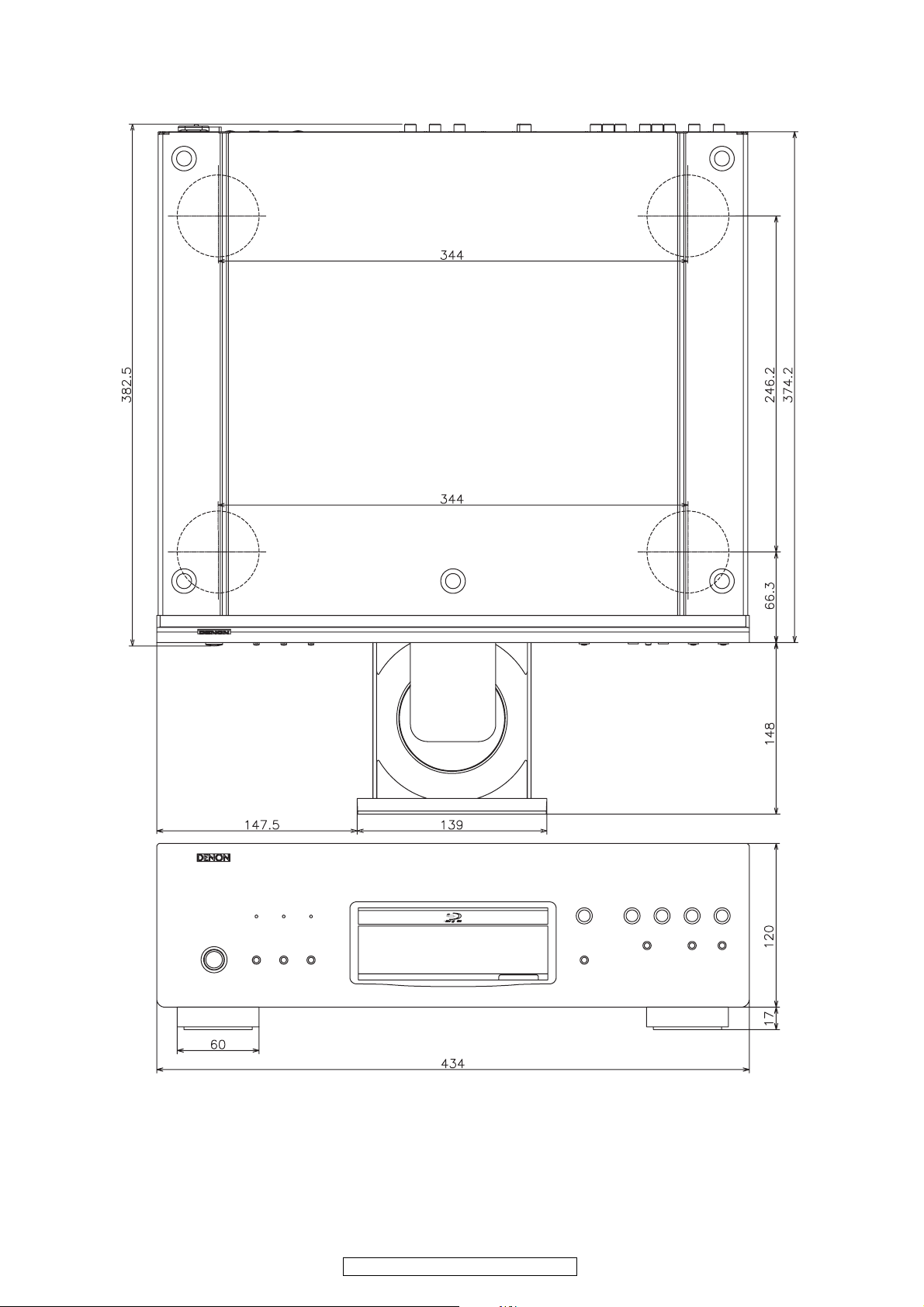
DIMENSION
3
DBP-4010UDCI/DBP-4010UD
Page 4
WIRE ARRANGEMENT
If wire bundles are untied or moved to perform adjustment or parts replacement etc., be sure to rearrange them neatly as they
were originally bundled or placed afterward.
Otherwise, incorrect arrangement can be a cause of noise generation.
Wire arrangement viewed from the top
Front Panel side
Back Panel side
4
DBP-4010UDCI/DBP-4010UD
Page 5
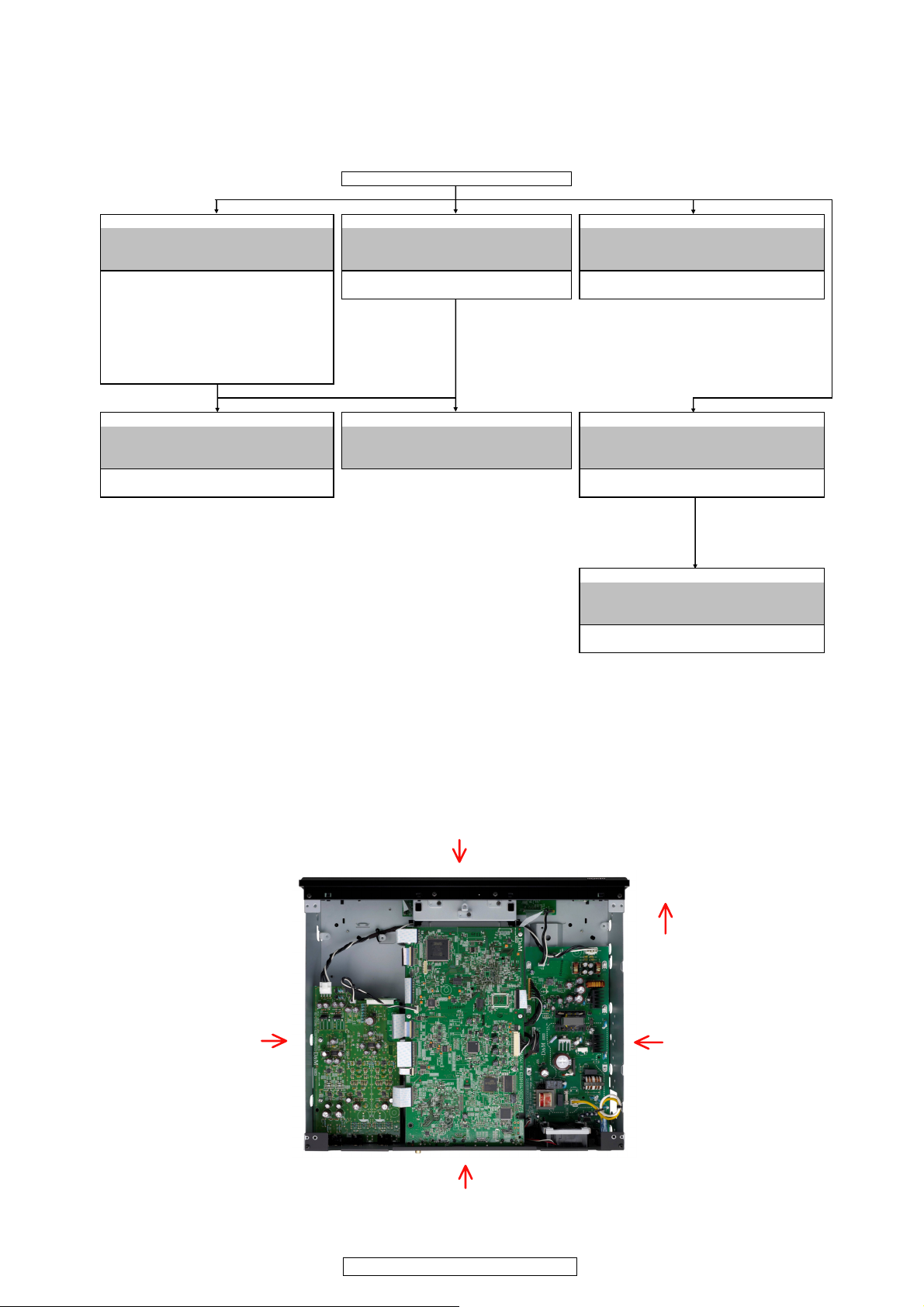
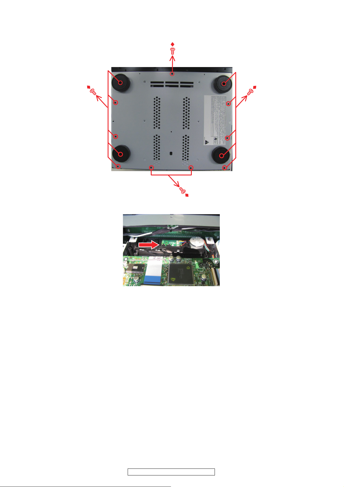
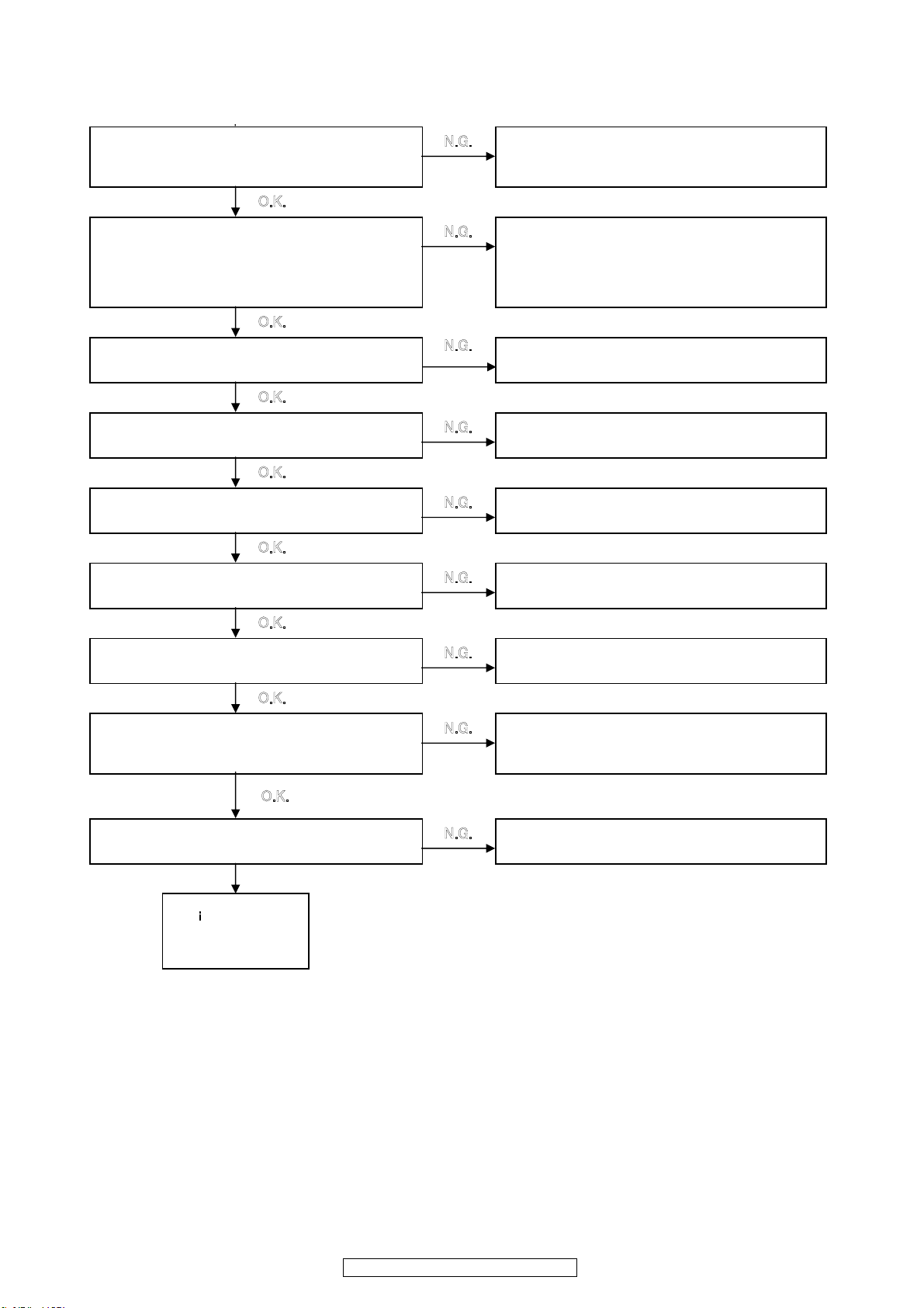
DISASSEMBLY
• Disassemble in order of the arrow of the figure of following flow.
• In the case of the re-assembling, assemble it in order of the reverse of the following flow.
• In the case of the re-assembling, observe "attention of assembling" it.
TOP COVER
FRONT PANEL ASSY MAIN UNIT ASSY POWER UNIT ASSY
Refer to "DISASSEMBLY Refer to "DISASSEMBLY Refer to "DISASSEMBLY
1.FRONT PANEL UNIT ASSY" 2.MAIN UNIT ASSY" 3.POWER UNIT ASSY"
DISPLAY UNIT ASSY MAIN UNIT ASSY POWER UNIT ASSY
(Ref. No. of EXPLODED VIEW : 12) (Ref. No. of EXPLODED VIEW : 29) (Ref. No. of EXPLODED VIEW : 23)
LED UNIT ASSY
(Ref. No. of EXPLODED VIEW : 11)
POWER SW UNIT ASSY
(Ref. No. of EXPLODED VIEW : 10)
SD UNIT ASSY
(Ref. No. of EXPLODED VIEW : 14)
ANALOG VIDEO UNIT ASSY MIX UNIT ASSY
(Ref. No. of EXPLODED VIEW : 27) (Ref. No. of EXPLODED VIEW : 25)
and "EXPLODED VIEW" and "EXPLODED VIEW" and "EXPLODED VIEW"
ANALOG VIDEO UNIT ASSY MECHA ASSY MIX UNIT ASSY
Refer to "DISASSEMBLY Refer to "DISASSEMBLY Refer to "DISASSEMBLY
6.ANALOG VIDEO UNIT ASSY" 7.CHASSIS BACK" 4.MIX UNIT ASSY"
and "EXPLODED VIEW" and "EXPLODED VIEW" and "EXPLODED VIEW"
SURROND UNIT ASSY
Refer to "DISASSEMBLY
5.SURROUND UNIT ASSY"
SURROND UNIT ASSY
(Ref. No. of EXPLODED VIEW : 24)
and "EXPLODED VIEW"
About the photos used for descriptions in the “DISASSEMBLY” section.
• The direction from which the photographs used herein were photographed is indicated at "Direction of photograph: ***" at
the left of the respective photographs.
• Refer to the table below for a description of the direction in which the photos were taken.
• Photographs for which no direction is indicated were taken from above the product.
• The photograph is DBP-4010UD.
The viewpoint of each photograph
(Photografy direction)
[View from above]
Direction of photograph: B
Front side
Direction of photograph: C
Direction of photograph: D
Direction of photograph: A
5
DBP-4010UDCI/DBP-4010UD
Page 6
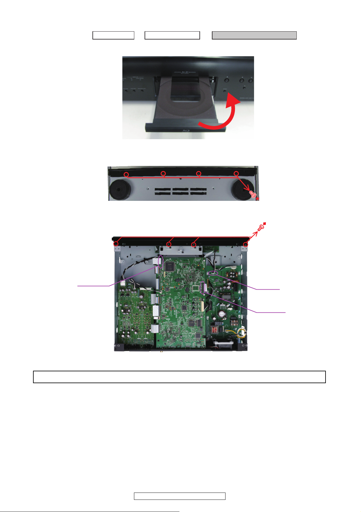
1. FRONT PANEL ASSY
Proceeding : TOP COVER →→
(1) Remove the Loadr Panel.
Direction of photograph: B
(2) Remove the screws. Disconnect the connector wire and FFC Cable.
View from bottom
LOADER PANEL FRONT PANEL UNIT ASSY
(3) Remove the screws. Disconnect the connector wire and FFC Cable.
FFC Cable
Please refer to "EXPLODED VIEW" for the disassembly method of each P.W.B included in FRONT PANEL ASSY.
CX042
FFC Cable
6
DBP-4010UDCI/DBP-4010UD
Page 7
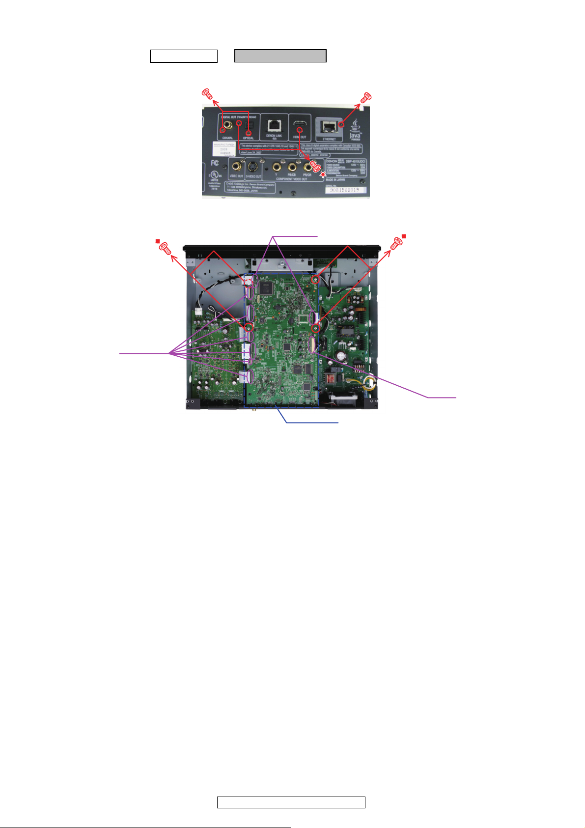
2. MAIN UNIT SUB ASSY
Proceeding : TOP COVER → MAIN UNIT ASSY
(1) Remove the screws.
ً
Direction of photograph: A
(2) Remove the screws. Disconnect the connector wires and FFC cables.
FFC Cable
◆
FFC Cable
CY151
MAIN UNIT
7
DBP-4010UDCI/DBP-4010UD
Page 8
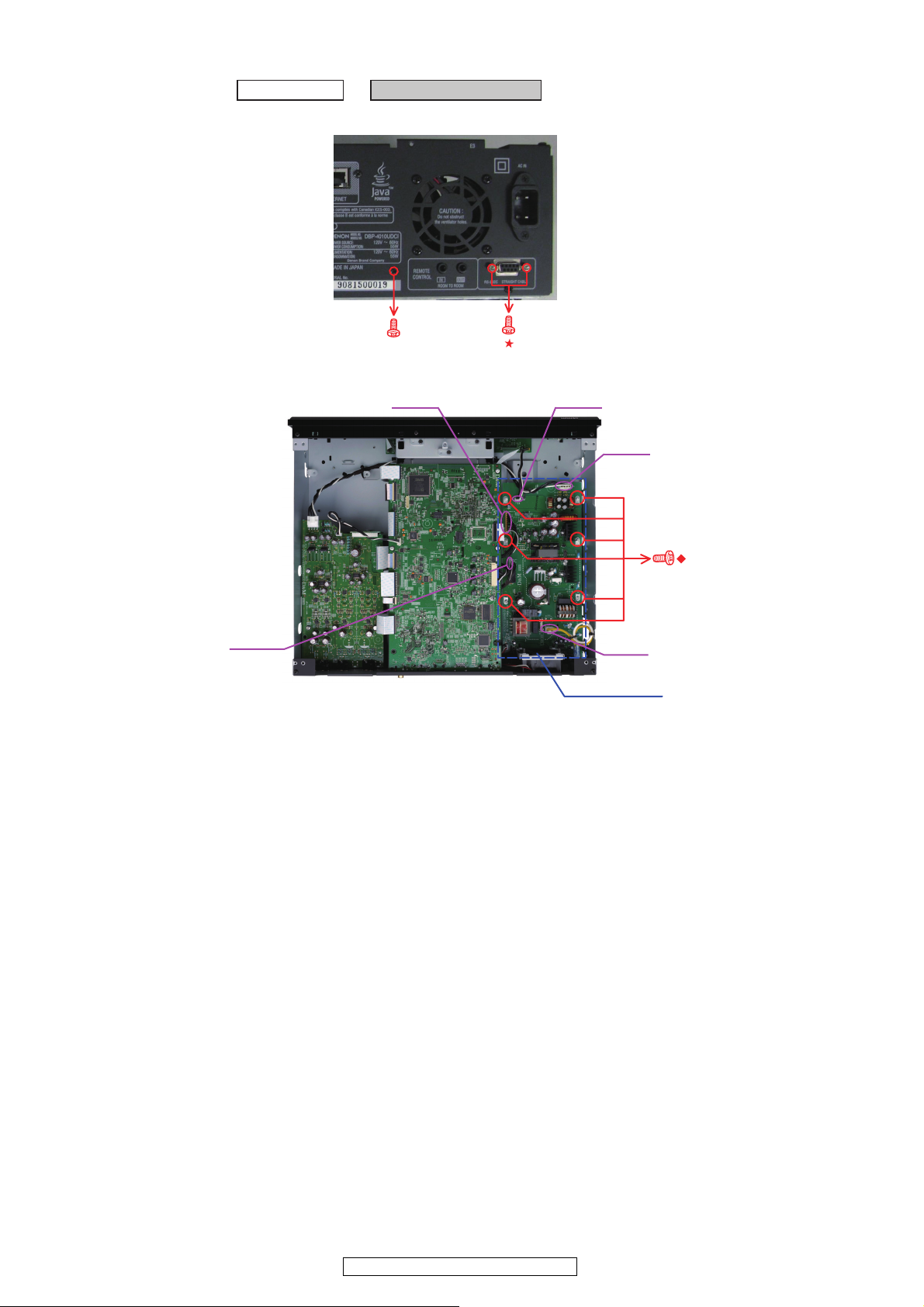
3.POWER UNIT ASSY
Proceeding : TOP COVER →
(1) Remove the screws.
Direction of photograph: A
(2) Remove the screws. Disconnect the connector wire.
POWER UNIT ASSY
◆
CX151
CX042
CX041
CY063
CX021
POWER UNIT
8
DBP-4010UDCI/DBP-4010UD
Page 9
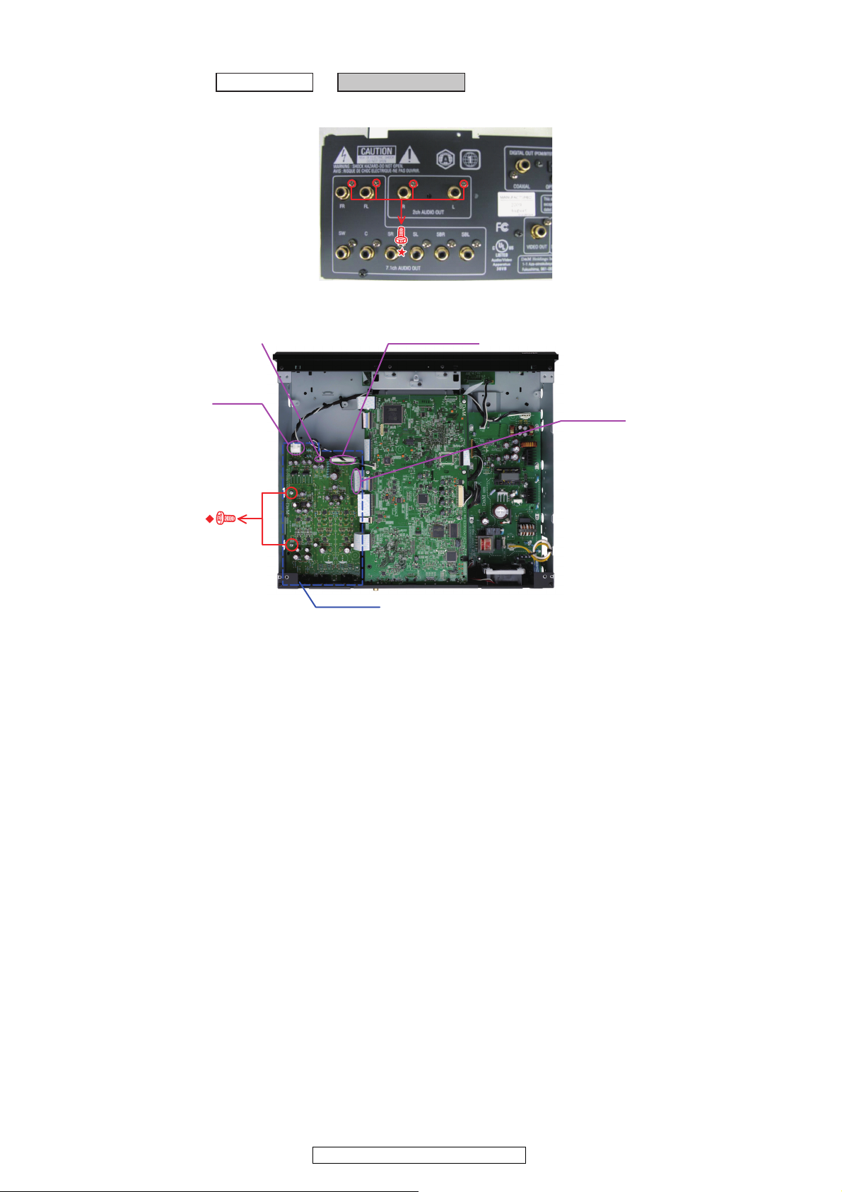
4. MIX UNIT ASSY
Proceeding : TOP COVER →
(1) Remove the screws.
Direction of photograph: A
(2) Remove the screws. Disconnect the connector wire and FFC Cable.
CY031
CY041
MIX UNIT ASSY
Board to Board
FFC Cable
MIX UNIT
9
DBP-4010UDCI/DBP-4010UD
Page 10
5. SURROUND UNIT ASSY
Proceeding : TOP COVER →→
(1) Remove the screws.
Direction of photograph: A
(2) Remove the screws.
MIX UNIT ASSY SURROUND UNIT ASSY
SURROUND UNIT
10
DBP-4010UDCI/DBP-4010UD
Page 11
6. ANALOG VIDEO UNIT
Proceeding : TOP COVER →→ MAIN UNIT ASSY ANALOG VIDEO UNIT ASSY
(1) Remove the screws.
Direction of photograph: A
(2) Remove the screws.
ANALOG VIDEO UNIT
7. MECHA ASSY
Proceeding : TOP COVER →→ MAIN UNIT ASSY MECHA ASSY
(1) Remove the screws.Disconnect the connector wire.
CY063
MECHA ASSY
11
DBP-4010UDCI/DBP-4010UD
Page 12
Removing discs
(1) Remove the screws and FOOTs.
View from bottom
(2) Slide the SLIDE CAM in the direction of the arrow.
Direction of photograph: A
(3) Draw out the LOADER TRAY, then remove the disc.
12
DBP-4010UDCI/DBP-4010UD
Page 13
DIAGNOSTICS OF OPTICAL PICKUP
DIAGNOSTICS OF OPTICAL PICKUP AND REPLACING FE MAIN P.W.B AND BD MECHANISM UNIT ASSY
Make failure diagnostics of the Optical Pickup as follows.
If the laser drive current (Iop) becomes more than ± 12[mA] of the initial value, the Optical Pickup should be replaced.
The laser drive current initial value is checked by "Iop checked Method" of next page.
In case of replacing the Pickup, change the whole part of the FE Main P.W.B and BD Mechanism Unit Assy.
No mechanical adjustment is necessary after the replacement.
Laser drive current initial value:
FL Display (The display part of 13 digits)
1 2 3 4 5 6 7 8 9 10 11 12 13
T 2 1 - m m m m - n n n n
FL Display (The display part of 13 digits)
1 2 3 4 5 6 7 8 9 10 11 12 13
T 2 2 - m m m m - n n n n
FL Display (The display part of 13 digits)
1 2 3 4 5 6 7 8 9 10 11 12 13
T 2 3 - m m m m - n n n n
FL Display (The display part of 13 digits)
1 2 3 4 5 6 7 8 9 10 11 12 13
T 2 4 - m m m m - n n n n
Disc no read, unsteady playback, etc.
Laser drive current (Iop) check
HF wave form check
(Refer to WAVE FORMS)
FE Main P.W.B. and BD Mechanism Unit
Assy replacing
Current value of the BD, DVD or CD IOP is
± 12[mA] or more the initial value.
CD:
DVD:
BD(SL):
BD(DL):
AND REPLACING FE MAIN P.W.B AND BD MECHANISM UNIT ASSY
Make failure diagnostics of the Optical Pickup as follows.
If the laser drive current (Iop) becomes more than ±12[mA] of the initial value, the Optical Pickup should be replaced.
The laser drive current initial value is checked by "Iop checked Method" of next page.
In case of replacing the Pickup, change the whole part of the FE Main P.W.B and BD Mechanism Unit Assy.
No mechanical adjustment is necessary after the replacement.
Laser drive current initial value:
DBP-4010UDCI/DBP-4010UD
13
Page 14
Iop checked Method
1.Iop checked Method
Select the laser ON/OFF(CD/DVD/BD)mode of the test mode, and check the IOP value of CD laser, DVD laser or BD
laser.
(See page 19 for test mode.)
FL Display (The display part of 13 digits)
1 2 3 4 5 6 7 8 9 10 11 12 13
T 2 L a s e r O n O f f
1.Iop checked Method
Select the laser ON/OFF(CD/DVD/BD)mode of the test mode, and check the IOP value of CD laser, DVD laser or BD
laser.
(See page 19 for test mode.)
DVDlasercurrentcheck
Press the 8 or 9 button to display the laser current value, and then select [X].
Check the current value of Iop (nnnn).
FL Display (The display part of 13 digits)
1 2 3 4 5 6 7 8 9 10 11 12 13
T 2 L a s e r O n O f f
FL Display (The display part of 13 digits)
1 2 3 4 5 6 7 8 9 10 11 12 13
T 2 X - m m m m - n n n n
1.Iop checked Method
Select the laser ON/OFF(CD/DVD/BD)mode of the test mode, and check the IOP value of CD laser, DVD laser or BD
laser.
(See page 19 for test mode.)
DVDlasercurrentcheck
Press the 8 or 9 button to display the laser current value, and then select [X].
Check the current value of Iop (nnnn).
(X=1 : CD laser mode, 2 : DVD laser mode, 3 : BD(SL) laser mode, 4 : BD(DL) laser mode)
(nn.nn[mA] : Current value)
2. To clear the accumulated laser on time
Press the 1 button while the accumulated laser on time is displayed ("TC1, "TC2", "TC3" ) until " * " appears at the fourth
position. Press the 8 or 9 button to select "TC4".If the 1 button is pressed while "TC1" is displayed, the accumu-
lated laser on time of CD, DVD and BD is cleared.
FL Display (The display part of 13 digits)
1 2 3 4 5 6 7 8 9 10 11 12 13
T 2 L a s e r O n O f f
FL Display (The display part of 13 digits)
1 2 3 4 5 6 7 8 9 10 11 12 13
T 2 X - m m m m - n n n n
FL Display (The display part of 13 digits)
1 2 3 4 5 6 7 8 9 10 11 12 13
T C 4 * - - - - - - - - -
1.Iop checked Method
Select the laser ON/OFF(CD/DVD/BD)mode of the test mode, and check the IOP value of CD laser, DVD laser or BD
laser.
(See page 19 for test mode.)
DVDlasercurrentcheck
Press the 8 or 9 button to display the laser current value, and then select [X].
Check the current value of Iop (nnnn).
(X=1 : CD laser mode, 2 : DVD laser mode, 3 : BD(SL) laser mode, 4 : BD(DL) laser mode)
(nn.nn[mA] : Current value)
2. To clear the accumulated laser on time
Press the 1 button while the accumulated laser on time is displayed ("TC1, "TC2", "TC3" ) until " * " appears at the fourth
position. Press the 8 or 9 button to select "TC4".If the 1 button is pressed while "TC1" is displayed, the accumu-
lated laser on time of CD, DVD and BD is cleared.
When “TC1”, “TC2” or “TC3” is selected with the 8 or 9 button, "mmmmmm" is displayed as “0” so you can check.
FL Display (The display part of 13 digits)
1 2 3 4 5 6 7 8 9 10 11 12 13
T 2 L a s e r O n O f f
FL Display (The display part of 13 digits)
1 2 3 4 5 6 7 8 9 10 11 12 13
T 2 X - m m m m - n n n n
FL Display (The display part of 13 digits)
1 2 3 4 5 6 7 8 9 10 11 12 13
T C 4 * - - - - - - - - -
FL Display (The display part of 13 digits)
1 2 3 4 5 6 7 8 9 10 11 12 13
T C Y - - - m m m m m m h
1.
Select the laser ON/OFF(CD/DVD/BD)mode of the test mode, and check the IOP value of CD laser, DVD laser or BD
laser.
(See page 19 for test mode.)
DVD laser current check
Press the 8 or 9 button to display the laser current value, and then select [X].
Check the current value of Iop (nnnn)
(X=1 : CD laser mode, 2 : DVD laser mode, 3 : BD(SL) laser mode, 4 : BD(DL) laser mode)
(nn.nn[mA] : Current value)
To clear the accumulated laser on time
2.
Press the 1 button while the accumulated laser on time is displayed ("TC1, "TC2", "TC3" ) until "*" appears at the
fourth position. Press the 8 or 9 button to select "TC4". If the 1 button is pressed while "TC1" is displayed, the
accumulated laser on time of CD, DVD and BD is cleared
When "TC1", "TC2" or "TC3" is selected with the 8 or 9 button, "mmmmmm" is displayed as "0" so you can check.
(Y=1 : CD, 2 : DVD , 3 : BD, mmmmmm : Time(Fractions of hours are counted up one hour on the display.)
14
DBP-4010UDCI/DBP-4010UD
Page 15
SERVICE MODE
1. Heat run mode
1.1. preparation
(1) Equipment used : Heat run disc (This operation may not work with any discs other than the heat run discs listed
below.)
CD : CD TEST DISC (TCD-HR01)
DVD :DVD TEST DISC (TDV-HR01)
BD :BD TEST DISC (TBD-HR01)
(2) Unit setting : No spec other than the following procedure.
1.2. procedure
<Playback mode>
(1) Pressing the 5 and 1 buttons simultaneously, plug the AC cord into a power outlet.
When the heat run mode is set, the "1" and "3" indicators light.
(2) Press the 5 button and open a tray.
(3) Set a disc to the tray and press the 1 button once. The "1" and "3" indicators blink at the same time and heat run
operation starts.
DVD : After playback title-1 and title-10 of the disc, the tray opens and closes automatically, then playback the
title-1 and title-10 again.
CD/BD : The disc is played through once from title 1 through the last title, the tray opens and closes automatically,
then the disc is played through again from title 1 through the last title.
(4) This heat run operation continues automatically or it stops caused by an error. In case of some error, the following
error messages are displayed on the FL tube.
<Tray open/close mode>
(1) Pressing the 5 and 1 buttons simultaneously, plug the AC cord into a power outlet.
When the heat run mode is set, the "1" and "3" indicators light.
(2) Press the 5 button and open a tray.
(3) Set a disc to the tray and press the 1 button twice. The "1" and "3" indicators blinks alternately and heat run
operation starts.
CD/DVD/BD : After disc loading is complete, the tray opens and closes automatically, and disc loading is carried out
again.
(4) This heat run operation continues automatically or it stops caused by an error. In case of some error, the following
error messages are displayed on the FL tube.
If the Manual Search.FWD button is pressed during heat run, the repeat count of heat run operations is displayed as
b
(Cnt *********). Press the Manual Search.FWD button once more and the display returns to its original state.
No. Error contents FL display
1 Tray Error ERROR 01
2 Bad Disc ERROR 02
3 Search Error ERROR 03
4 Read Error ERROR 04
5 Communications error ERROR 05
6 Other (Front end error) ERROR 06
15
DBP-4010UDCI/DBP-4010UD
Page 16

2. Initial setting mode
2.1. preparation
(1) Equipment used: None
(2) Unit setting: No spec other than the following procedure.
2.2. procedure
Initialize the BD player when µcom, peripheral parts of µcom, or MAIN P.W.B. unit has been replaced in servicing.
b
All user setting will be lost and its factory setting will be restored when this initialization is made. Be sure to memorize
b
your setting for restoring again after the initialization.
(1)TurnontheDBP-4010UDCI/DBP-4010UD'spower."NODISC"isdisplayedontheuorescenttube.
(2) Press the DBP-4010UDCI/DBP-4010UD's PLAY, EJECT and Disc layer buttons simultaneously. "INITIALIZING" is
displayedontheuorescenttube.
(3)Thedisplayontheuorescenttubeswitchesto"INITIALIZED",the"NODISC"displayreappearsandinitializationis
completed.
3. µcomrm,H/Wversion,andSerealnumbermode
3.1. preparation
(1) Equipment used: None
(2) Unit setting: No spec other than the following procedure.
3.2. procedure
Systemµcomandotherµcomrmcheckmode.
b
This mode is for displaying the status of each µcom employed.
(1) Pressing the 5 and 1 buttons simultaneously, plug the AC cord into a power outlet.
(2)"NODISC"isdisplayedontheuorescenttube.
(3) Press remote contraller "3265".
(4) Each time the POP UP MENU button or Cursor buttons(d or f) on the remote control unit is pressed, version
informationofµcomrm,versionofH/Wandserialnumberisdisplayedoneafteranother.
Ex.: [Sys Ver000103, Sys Day090219, Sys GEN100000………, H/W Ver000000, S/N ***************]
4. Tray lock mode
4.1. preparation
(1) Equipment used: None
(2) Unit setting: No spec other than the following procedure.
4.2. procedure
[Setting]
(1) Pressing the 1 and 3 buttons for simultaneously, plug the AC cord into a power outlet.
(2)"TRAYLOCK"isdisplayedontheuorescenttubeandtrayopening/closingisinvalidated.
[Cancel]
(1) Unplug the DBP-4010UDCI/DBP-4010UD's AC cord from the power outlet.
(2) Pressing the 1 and 3 buttons simultaneously, plug the AC cord into a power outlet.
(3)"PLEASEWAIT"isdisplayedontheuorescenttubeandtrayopening/closingisenabled.
The tray lock mode is also canceled when the product is initialized.
b
16
DBP-4010UDCI/DBP-4010UD
Page 17

5. Remote lock mode
5.1. preparation
(1) Equipment used: None
(2) Unit setting: No spec other than the following procedure.
5.2. procedure
[Setting]
(1) Pressing the PURE DIRECT, 5 and SOURCE buttons for simultaneously.
(2) “Lock-On” is displayed on the FL tube, and operations with the remote control and the REMOTE CONTROL input
terminal on the back of the DBP-4010UD are disabled.
[Cancel]
(1) Pressing the PURE DIRECT, 5 and SOURCE buttons for simultaneously.
(2)"Lock-Off"isdisplayedontheuorescenttubeandremotelockmodeismadecanceled.
All Lit / All Off mode for the FL tube
6.
6.1. preparation
(1) Equipment used: None
(2) Unit setting: No spec other than the following procedure.
6.2. procedure
[Setting]
(1) Pressing the Manual Search RVS and 1 buttons for simultaneously, plug the AC cord into a power outlet.
If All Lit / All Off mode is set for the FL tube, the FL tube’s display area is fully lit.
(2) Press the Pure Direct button to switch between ‘all lit’ and ‘all off’ display.
[Cancel]
(1) Remove the power cable for 5 seconds or more to cancel All Lit / All Off mode for the FL tube.
Forced Tray Open mode.
7.
7.1. preparation
(1) Equipment used: None
(2) Unit setting: No spec other than the following procedure.
Operation cannot be guaranteed after executing Forced Tray Open mode.
b
7.2. procedure
[Setting]
To forcibly open the tray, press the 5 for 5 seconds or more.
(1)
[Cancel]
(1) Remove the power cable for 5 seconds or more to cancel Forced Tray Open mode.
17
DBP-4010UDCI/DBP-4010UD
Page 18
8. Test mode
8.1. Entering the test mode
The test mode is entered by pressing the 5 and 2 buttons simultaneously, plug the AC cord into a power outlet.
When the test mode is set, the "1" and "3" indicators light.
FL tube display when test mode entered
FL Display (The display part of 13 digits)
1 2 3 4 5 6 7 8 9 10 11 12 13
T E S T M O D E
When the test mode is set, a color bar appears on the monitor.
8.2. Selecting the mode
The following modes are available.
・
(1) Laser on/off (CD/DVD/BD) mode : T2
(2) Servo adjustment value display mode : T3
(3) Error rate (skew) measurement mode : T7
(4) Accumulated laser on time display mode : TC
(5) Track buffer output mode : TE
(6) Picking up No. display mode : TG
(7) Error log display mode : TH
(8) Test mode cancel : TI
When the 9 button is pressed after entering the test mode, the display switches in the order: "T2, T3, T7, TC, TE,
q
TG, TH, TI, T2 …"
FL Display (The display part of 13 digits)
1 2 3 4 5 6 7 8 9 10 11 12 13
T 2 L a s e r O n O f f
FL Display (The display part of 13 digits)
1 2 3 4 5 6 7 8 9 10 11 12 13
T 3 S e r v o A d j .
FL Display (The display part of 13 digits)
1 2 3 4 5 6 7 8 9 10 11 12 13
T 7 E r r o r R a t e
FL Display (The display part of 13 digits)
1 2 3 4 5 6 7 8 9 10 11 12 13
T C L a s e r O n T i m
FL Display (The display part of 13 digits)
1 2 3 4 5 6 7 8 9 10 11 12 13
T E T r a c k B u f
FL Display (The display part of 13 digits)
1 2 3 4 5 6 7 8 9 10 11 12 13
T G O P U N u m b e r
FL Display (The display part of 13 digits)
1 2 3 4 5 6 7 8 9 10 11 12 13
T H E r r o r L o g
FL Display (The display part of 13 digits)
1 2 3 4 5 6 7 8 9 10 11 12 13
T I T e s t E x i t
When the 8 button is pressed, the display switches in the opposite order fromq above, starting from the current
w
position (for example, if currently at "TA", it switches as follows: "T2, T3, T7, TC, TE, TG, TH, TI, T2 …").
18
DBP-4010UDCI/DBP-4010UD
Page 19
8.3. About each mode
With the mode selected, press the 1 button to set that mode.
・
(1) Laser on/off (CD/DVD/BD) mode
Press the 8 or 9 button to select [X] and press the 1 button to set it.
Laser on/off control is executed and the laser current is displayed.
FL Display (The display part of 13 digits)
1 2 3 4 5 6 7 8 9 10 11 12 13
T 2 X m m m m n n n n
(X=1 : CD laser mode, 2 : DVD laser mode, 3 : BD(SL) laser mode, 4 : BD(DL) laser mode)
(mm.mm[mA] : Stored data, nn.nn[mA] : Current value)
When the current value is more that ± 12.00[mA] of saved data, it becomes the pickup transducer's target.
b
In this case, replace the mechanism unit.
If stored value is not
FL Display (The display part of 13 digits)
1 2 3 4 5 6 7 8 9 10 11 12 13
T 2 X
― ― ― ― ― ―
(X=1 : CD laser mode, 2 : DVD laser mode, 3 : BD(SL) laser mode, 4 : BD(DL) laser mode)
(nn.nn[mA] : Current value)
When the 2 button is pressed, the layer above the current layer is displayed. See "8.4 Stopping the mode" (page
22).
n n n n
(2) Servo adjustment value display mode
Press the 8 or 9 button to select [XXX]. Refer to [Table 1 - Servo adjustment value display mode details] (page
22).
FL Display (The display part of 13 digits)
1 2 3 4 5 6 7 8 9 10 11 12 13
T X X X
(XXX : Servo adjustment value
Press the 1 button to set. The contents indicated on "Table 1: Details of the servo adjustment value display mode"
(page 22) are displayed.
FL Display (The display part of 13 digits)
1 2 3 4 5 6 7 8 9 10 11 12 13
)
T X X X m m m m m m n n
(XXX : Selection mode, mmmmmm : Address(HEX), nn:Data(HEX))
Thersttime,theaddressspeciciationpositionistheuppermostposition(5thplace).Theaddressspeciciation
position moves downwards each time the 1 button is pressed.
Theaddressspeciciationpositionashes(atanintervalofabout0.5seconds).Ifthe1buttonispressedafter
moving to the lowermost position (10th place), the position moves to the uppermost position
Use the 8 or 9buttontochangethedisplayattheaddressspecicationposition.
When the 2 button is pressed, the layer above the current layer is displayed. See "8.4 Stopping the mode" (page
22).
19
DBP-4010UDCI/DBP-4010UD
Page 20
(3) Error rate measurement mode
Press the 8 or 9 button to select [YY] .
Refer to [Table 2 - Error rate details]. (page 23)
FL Display (The display part of 13 digits)
1 2 3 4 5 6 7 8 9 10 11 12 13
T Y Y F F F F F F F F F F
(X : measurement mode, F : Address and error rate (When not set, "F" is displayed.)
Press the 1 button to begin error rate measurement. The address and error rate are displayed.
For a description of the displayed measurement results, see "Table 2: Error rate details" (page 23).
FL Display (The display part of 13 digits)
1 2 3 4 5 6 7 8 9 10 11 12 13
T Y Y m m m m m m
(YY : selection mode [71 to 94], m : address [PBA][HEX], l : error rate [COUNT/SEC] [HEX])
(Note) CD (4x-speed) : Renewal of data is carried out for every 300 frame.
Error rate of 75 frames is displayed.
DVD (2x-speed) : Renewal of data is carried out for every 80ECC block.
Error rate of 8ECC block is displayed.
BD (2x-speed) : Renewal of data is carried out for every 136LDC clusters block.
Error rate of 8LDC clusters block is displayed.
The mode chosen when selection mode was changed into the trace execution and the 1 button was pushed is
performed from the beginning.
When the 1 button is pushed without changing selection mode, the mode under selection is performed from the
beginning.
(If the 1 button is pushed, the address corresponding to the chosen mode will be searched again.)
The pause mode is set after tracing is completed.
When the 2 button is pressed, the layer above the current layer is displayed. See "8.4 Stopping the mode" (page
22).
l l l l
(4) Accumulated laser on time display mode
Press the 8 or 9 button to select [Y] and press the 1 button to set it.
The accumulated laser on time is displayed.
FL Display (The display part of 13 digits)
1 2 3 4 5 6 7 8 9 10 11 12 13
T C Y m m m m m m h
(Y=1 : CD, 2 : DVD , 3 : BD, mmmmmm : Time(Fractions of hours are counted up one hour on the display.)
When the 2 button is pressed, the layer above the current layer is displayed. See "8.4 Stopping the mode" (page
22)
---To clear the accumulated laser on time---
Press the 1 button while the accumulated laser on time is displayed ("TC1, "TC2", "TC3" ) until "*" appears at
the fourth position.
FL Display (The display part of 13 digits)
1 2 3 4 5 6 7 8 9 10 11 12 13
T C Y * m m m m m m
Press the 8 or 9 button to select "TC4"
FL Display (The display part of 13 digits)
1 2 3 4 5 6 7 8 9 10 11 12 13
T C 4 *
If the 1 button is pressed while "TC4" is displayed, the accumulated laser on time of CD, DVD and BD is cleared.
FL Display (The display part of 13 digits)
1 2 3 4 5 6 7 8 9 10 11 12 13
T C 1 0 0 0 0 0 0 h
When "TC1", "TC2" or "TC3" is selected with the 8 or 9 button, "mmmmmm" is displayed as "0" so you can
check.
20
DBP-4010UDCI/DBP-4010UD
Page 21
(5) Track buffer output mode
Press the 8 or 9 button to select "Y" and switch the track buffer output.
FL Display (The display part of 13 digits)
1 2 3 4 5 6 7 8 9 10 11 12 13
T E Y T r a c k B u f f
(Y=1 : Track buffer being output, 0 : Track buffer output off )
When the 2 button is pressed, the layer above the current layer is displayed. See "8.4 Stopping the mode" (page
22).
(6) Picking up No. display mode
Press the 8 or 9 button to switch to the pickup number display.
The pickup number is a 14-digit number, so it is displayed in two sections.
FL Display (The display part of 13 digits)
1 2 3 4 5 6 7 8 9 10 11 12 13
T G X Y Y Y Y Y Y Y
(X (display position) = 1 : Lower digits, 2 : Upper digits. YYYYYYY: Pickup number)
When the 2 button is pressed, the layer above the current layer is displayed. See "8.4 Stopping the mode" (page
22).
(7) Error log display mode
Press the 8 or 9 button to switch to the error log display.
For Error log No. and description of the displayed measurement results, see "Table 3: Error log details" (page 25).
FL Display (The display part of 13 digits)
1 2 3 4 5 6 7 8 9 10 11 12 13
n T H X
(n : Error information No.(1~5), X : Error log No.)
Display when there is no error
FL Display (The display part of 13 digits)
1 2 3 4 5 6 7 8 9 10 11 12 13
n T H 1 N o E r r o r
When the 2 button is pressed, the layer above the current layer is displayed. See "8.4 Stopping the mode" (page
22).
(8) Test mode cancel
A conrmation message is displayed. Press the 1 button to set, canceling the test mode.
FL Display (The display part of 13 digits)
1 2 3 4 5 6 7 8 9 10 11 12 13
T I 1 R e a l l y ?
When the 2 button is pressed, the layer above the current layer is displayed. See "8.4 Stopping the mode" (page
22).
21
DBP-4010UDCI/DBP-4010UD
Page 22

8.4. Stopping the mode
When the 2 button is pressed, the layer above the current layer is displayed. The relationship between the different
modes and the display of the different layers is shown on the table below.
Mode 1 layer 2 layer 3 layer
Laser on/off (CD/DVD/BD) mode T2 LaserOnOff T2X mmmm nnnn Non
Servo adjustment value display mode T3 Servo Adj. TXXX TXXXmmmmmm nn
Error rate (skew) measurement mode T7 Error Rate TYYFFFFFFFFFF TYYmmmmmmllll
Accumulated laser on time display mode TC LaserOnTim TCY mmmmmmh
Track buffer output mode TE Track Buf TEYTrack Buff Non
Picking up No. display mode TG OPU Number TGX YYYYYYY Non
Error log display mode TH Error Log
Test mode cancel TI Test Exit TI1 Really? Non
nTHX
nTH1 No Error
TCY* mmmmmmh
TC4*
nTHX dddddd
nTHAyyy dddd
8.5. About the OPEN/CLOSE (5)button
Even during the test mode, the tray is opened and closed when the 5 button is pressed.
8.6. Test mode detailed table
Table 1: Servo adjustment value display mode details
No XXX Name Address range Meaning
0 T30 BUF_ID_SDRAM 0x000000~0x3FFFFF SDRAM
1 T31 BUF_ID_MPU_ALL 0x000000~0xBEFF3F MPU(Abs Access)
2 T32 BUF_ID_MPU_RMCR 0x000000~0x00FFFF ROMCOR
3 T33 BUF_ID_MPU_SYSCFG 0x000000~0x000FFF SystemCongration
4 T34 BUF_ID_MPU_DMAC 0x000000~0x0004FF DMAC
5 T35A BUF_ID_MPU_ITIM0 0x000000~0x0000FF ITIM 0
6 T35B BUF_ID_MPU_ITIM1 0x000000~0x0000FF ITIM 1
7 T35C BUF_ID_MPU_ITIM2 0x000000~0x0000FF ITIM 2
8 T35D BUF_ID_MPU_ITIM3 0x000000~0x0000FF ITIM 3
9 T35E BUF_ID_MPU_ITIM4 0x000000~0x0000FF ITIM 4
10 T35F BUF_ID_MPU_ITIM5 0x000000~0x0000FF ITIM 5
11 T36 BUF_ID_MPU_RSV2 0x000000~0x0079FF Reserved
12 T37 BUF_ID_MPU_WDT 0x000000~0x000FFF WDT
13 T38 BUF_ID_MPU_UART0 0x000000~0x0000FF UART 0
14 T39 BUF_ID_MPU_UART1 0x000000~0x0000FF UART 1
15 T40 BUF_ID_MPU_CSIO0 0x000000~0x0000FF CSIO 0
16 T41 BUF_ID_MPU_CSIO1 0x000000~0x0000FF CSIO 1
17 T42 BUF_ID_MPU_GPIO0 0x000000~0x0000FF GPIO 0
18 T43 BUF_ID_MPU_GPIO1 0x000000~0x0000FF GPIO 1
19 T44 BUF_ID_MPU_GPIO2 0x000000~0x0000FF GPIO 2
20 T45 BUF_ID_MPU_RSV5 0x000000~0x00BCFF Reserved
21 T46 BUF_ID_MPU_HEXBIU 0x000000~0x000FFF HEXBIU
22 T47 BUF_ID_MPU_HCSC 0x000000~0x000FFF HCSC
23 T48 BUF_ID_MPU_RSV6 0x000000~0x7DDFFF Reserved
24 T49 BUF_ID_MPU_RSV7 0x000000~0x3DFEFF Reserved
25 T50 BUF_ID_MPU_INT 0x000000~0x00003F INT
26 T51 BUF_ID_IRAM 0x000000~0x003FFF IRAM(internal SRAM))
27 T52 BUF_ID_DSP 0x000000~0x001FFF DSP Register
28 T53 BUF_ID_AFE 0x000000~0x0000FF AFE Register
29 T54 BUF_ID_SVO_ALL 0x000000~0x001FFF SVO REG ABS ACCESS
30 T55 BUF_ID_SVO_REG 0x000000~0x0007FF SVERVO REG
22
DBP-4010UDCI/DBP-4010UD
Page 23

No XXX Name Address range Meaning
31 T56 BUF_ID_SVO_SVRAM 0x000000~0x0005FF SVRAM
32 T57A BUF_ID_SVO_CRAM0 0x000000~0x0001FF CRAM0
33 T57B BUF_ID_SVO_CRAM1 0x000000~0x0001FF CRAM1
34 T57C BUF_ID_SVO_CRAM2 0x000000~0x0001FF CRAM2
35 T57D BUF_ID_SVO_CRAM3 0x000000~0x0001FF CRAM3
36 T58A BUF_ID_SVO_ZRAM0 0x000000~0x0001FF ZRAM0
37 T58B BUF_ID_SVO_ZRAM1 0x000000~0x0001FF ZRAM1
38 T58C BUF_ID_SVO_ZRAM2 0x000000~0x0001FF ZRAM2
39 T58D BUF_ID_SVO_ZRAM3 0x000000~0x0001FF ZRAM3
40 T59 BUF_ID_EPRM 0x000000~0x000FFF EEPROM
41 T60 BUF_ID_PUCONT_LDD 0x000000~0x000007 LDD
42 T61 BUF_ID_SVRESULT 0x000000~0x0002C3 SvResult
43 T62 BUF_ID_LD_TIME 0x000000~0x00000D LD ON Time Integrated value
44 T63 BUF_ID_IOP 0x000000~0x000007 IOP(Stored value)
Table 2: Error rate details
Measurement
YY
71 The inner
72 The inner
73 The inner
74 The inner
75 The central
76 The central
77 The central
78 The central
79 The outer
80 The outer
81 The outer
82 The outer
position
circumference of
1-layer
circumference of
1-layer
circumference of
1-layer
circumference of
1-layer
circumference of
1-layer
circumference of
1-layer
circumference of
1-layer
circumference of
1-layer
circumference of
1-layer
circumference of
1-layer
circumference of
1-layer
circumference of
1-layer
Error rate display details for each media type
BD DVD CD
BIS error detection
signed number
BIS error uncorrectable
signed numbe
LDC error detection
signed number
LDC error uncorrectable
signed numbe
BIS error detection
signed number
BIS error uncorrectable
signed numbe
LDC error detection
signed number
LDC error uncorrectable
signed numbe
BIS error detection
signed number
BIS error uncorrectable
signed numbe
LDC error detection
signed number
LDC error uncorrectable
signed numbe
Remarks
It is invalid. It is invalid. When this is selected for DVD or CD,
it shifts to YY=73.
It is invalid. It is invalid. When this is selected for DVD or CD,
it shifts to YY=73.
PI error detection
number
PO uncorrectable
error number
It is invalid. It is invalid. When this is selected for DVD or CD,
It is invalid. It is invalid. When this is selected for DVD or CD,
PI error detection
number
PO uncorrectable
error number
It is invalid. It is invalid. When this is selected for DVD or CD,
It is invalid. It is invalid. When this is selected for DVD or CD,
PI error detection
number
PO uncorrectable
error number
C1 error
detection number
C2 uncorrectable
error number
it shifts to YY=77.
it shifts to YY=77.
C1 error
detection number
C2 uncorrectable
error number
it shifts to YY=81.
it shifts to YY=81.
C1 error
detection number
C2 uncorrectable
error number
23
DBP-4010UDCI/DBP-4010UD
Page 24

Measurement
YY
83 The inner
84 The inner
85 The inner
86 The inner
87 The central
88 The central
89 The central
90 The central
91 The outer
92 The outer
93 The outer
94 The outer
position
circumference of
2-layer
circumference of
2-layer
circumference of
2-layer
circumference of
2-layer
circumference of
2-layer
circumference of
2-layer
circumference of
2-layer
circumference of
2-layer
circumference of
1-layer
circumference of
1-layer
circumference of
1-layer
circumference of
1-layer
Error rate display details for each media type
BD DVD CD
BIS error detection
signed number
BIS error uncorrectable
signed number
LDC error detection
signed number
LDC error uncorrectable
signed numbe
BIS error detection
signed number
BIS error uncorrectable
signed numbe
LDC error detection
signed number
LDC error uncorrectable
signed numbe
BIS error detection
signed number
BIS error uncorrectable
signed numbe
LDC error detection
signed number
LDC error uncorrectable
signed numbe
Remarks
It is invalid. It is invalid. When this is selected for 2-layer DVD,
it shifts to YY=85.
When this is selected for 1-layer DVD
or CD, it shifts to YY=73.
It is invalid. It is invalid. When this is selected for DVD 2-layer,
it shifts to YY=85.
When this is selected for DVD 1-layer
or CD, it shifts to YY=73.
PI error detection
number
PO uncorrectable
error number
It is invalid. It is invalid. When this is selected for DVD
It is invalid. It is invalid. When this is selected for DVD 2-layer,
PI error detection
number
PO uncorrectable
error number
It is invalid. It is invalid. When this is selected for DVD 2-layer,
It is invalid. It is invalid. When this is selected for DVD 2-layer,
PI error detection
number
PO uncorrectable
error number
It is invalid. When this is selected for 1-layer DVD
or CD, it shifts to YY=73.
It is invalid. When this is selected for 1-layer DVD
or CD, it shifts to YY=73.
2-layer, it shifts to YY=89.When this
is selected for DVD 1-layer or CD, it
shifts to YY=77.
it shifts to YY=89.
When this is selected for DVD 1-layer
or CD, it shifts to YY=77.
It is invalid. When this is selected for DVD 1-layer
or CD, it shifts to YY=77.
It is invalid. When this is selected for DVD 1-layer
or CD, it shifts to YY=77.
it shifts to YY=93.
When this is selected for DVD 1-layer
or CD, it shifts to YY=81.
it shifts to YY=93.
When this is selected for DVD 1-layer
or CD, it shifts to YY=81.
It is invalid. When this is selected for DVD 1-layer
or CD, it shifts to YY=81.
It is invalid. When this is selected for DVD 1-layer
or CD, it shifts to YY=81.
* The inner circumference of the layer refers to the physical inner circumference for DVD parallel, the physical outer
circumference for the opposite case.
* The inner circumference of the layer refers to the physical outer circumference for DVD parallel, the physical inner
circumference for the opposite case.
24
DBP-4010UDCI/DBP-4010UD
Page 25
Table 3: Error log details
Error log No.
1 LD On Time (4Byte)
2 Error type (2Byte) See "Table 3-1: Error type details"
3 (31 to 34 displayed in 4-byte units) Reserve (16Byte)
4 Media type (2Byte) See "Table 3-2: Media type details"
5 Reserve (4Byte)
6 Reserve (4Byte)
7 Reserve (2Byte)
8 HyBrid Disc layer (2Byte) See "Table 3-3: HyBrid Disc current layer details"
9 (91 to 92 displayed in 7-digit units)
(Matched to TG pickup number display)
A (A000 to A161 displayed in 2-digit units) Reserve (708Byte)
B (B1 to B3 displayed in 4-digit units) Reserve (11Byte)
C Reserve (1Byte)
D (D1 to D3 displayed in 4-digit units) Reserve (12Byte)
PU# (16Byte)
Table 3-1: Error type details
Contents
(Error log overall layout)
Table 3-2: Media type details
Remarks
Error type Error code
NoError 0x0000
Focus does not turn on. 0x0001
Tracking does not turn on. 0x0002
CLV does not turn on. 0x0003
ID cannot be read. 0x0004
Loader error 0x0005
Thread error 0x0006
Expander error 0x0007
Other error 0x0008
Error disc (Failure to recognition of disc) 0x0009
Seek error 0x0010
Lead error 0x0020
Other Reserved
Table 3-3: HyBrid Disc current layer details
HyBrid Disc current layer Current layer code
SACD layer 0x0000
CD layer 0x0001
DVD layer 0x0002
BD layer 0x0003
Other Reserved
Media type Media code
DVD-ROM 0x0001
DVD-R 0x0002
DVD-RW 0x0003
DVD-PLUS-R 0x0004
DVD-PLUS-RW 0x0005
DVD-ROM DL 0x0006
DVD+R DL 0x0007
DVD-R DL 0x0008
DVD+RW DL 0x0009
DVD-RW DL 0x000A
CD-ROM 0x000B
CD-R 0x000C
CD-RW 0x000D
BD-RE SL 0x000E
BD-RE DL 0x000F
BD-R SL 0x0010
BD-R DL 0x0011
BD-R SL LTH 0x0012
BD-ROM SL 0x0013
BD-ROM DL 0x0014
BD-Hybrid 0x0015
SACD-Hybrid 0x0016
SACD DL 0x0017
SACD SL 0x0018
DVD-Hybrid 0v0019
Unknown 0xFFFF
Other Reserved
25
DBP-4010UDCI/DBP-4010UD
Page 26
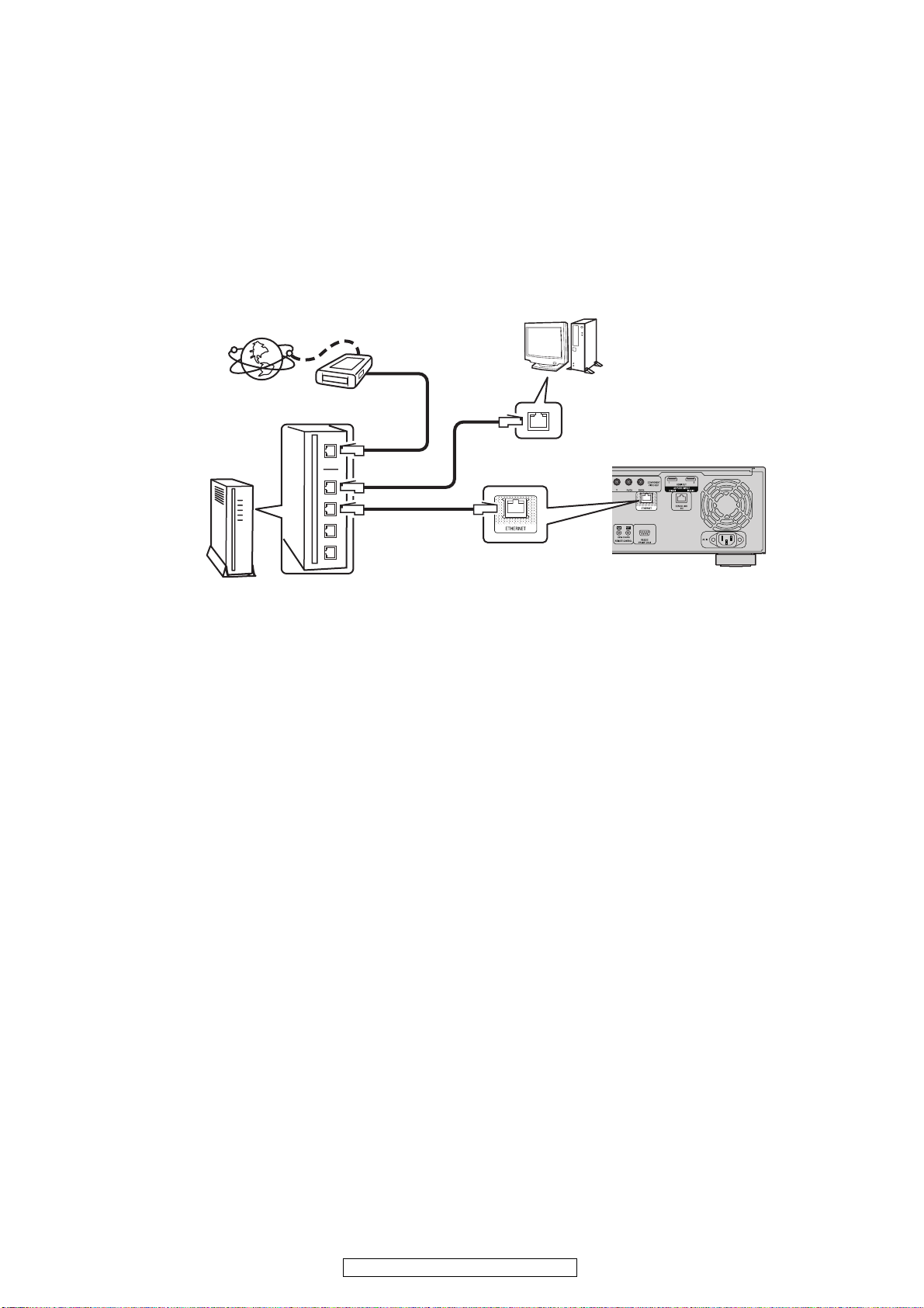
VERSION UPGRADE PROCEDURE OF FIRMWARE
You can update by downloading the latest firmware from the Internet.
To update the IP ROM, refer to "Updating the IP ROM" on page 28.
1.Update from the Internet
1.1. Connecting to the Network
(1) System Requirement
• Internet Connection by Broadband Circuit
• Modem
• Router
• Ethernet cable (CAT-5 or greater recommended)
(2) Setting
Internet
Computer
Router
Modem
To WAN port
To LAN port
To LAN port
ETHERNET
connector
LAN port/
Ethernet
connector
1.2. Check for Update and Update
Check if the latest firmware exists. You can also check approximately how long it will take to complete an update.
(1) Press the SETUP button on the remote control to display the GUI menu.
(2) Use the cursor buttons to select "Other settings" → "Firmware update" → "Update check".
(3) Press the ENTER buttom.
• The latest version of the firmware uploaded to the web is displayed.
• If the latest firmware version is on the web, proceed to (4).
• If the latest firmware is already installed, press the SETUP button to close the menu.
(4) Use the cursor buttons to select "Update", then press the ENTER button.
• During update, the power indicator lights red and the GUI screenis shut down. And a rough remaining time is
indicated on the display.
• When updating is complete the power indicator lights green and normal
• status is resumed.
(5) Press the SETUP button to close the menu.
--- Cautions on Firmware Update ---
• In order to use these functions, you must have the correct system requirements and settings for a broadband Internet
connection.
• Do not turn off the power until updating is completed.
Even with a broadband connection to the Internet, approximately about 1 hour is required for the updating procedure to be
completed.
Once updating starts, normal operations on the DVD-A1UD cannot be performed until updating is completed. Also, setting items of the GUI menu of DVD-A1UD or setting items of the image adjustment may be initialized.
Make a note of the settings before updating, and set them again after updating.
26
DBP-4010UDCI/DBP-4010UD
Page 27
TROUBLE SHOOTING
1. 8U-210086-1(MIXUNIT)/8U-210018-2(SURROUNDUNIT)
㪚㪿㪼㪺㫂㩷㪺㫆㫅㫅㪼㪺㫋㫀㫆㫅㩷㪙㪆㪜㩷㩷㪧㪮㪙㩷㪬㪥㪠㪫 㪚㪿㪼㪺㫂㩷㪪㫆㫃㪻㪼㫉㫀㫅㪾㪃㩷㪝㪝㪚㩷㪺㪸㪹㫃㪼
㪏㪬㪄㪊㪈㪇㪇㪋㪈㩿㪙㪆㪜㩷㪬㪥㪠㪫㪀
䊶㪲㪚㪯㪊㪊㪈㪴㩷㫀㫅㫇㫌㫋㩷㫊㫀㪾㫅㪸㫃㪅 䊶㪲㪚㪯㪊㪊㪉㪴㪑㪏㪬㪄㪊㪈㪇㪇㪋㪈
䊶㪲㪚㪯㪊㪊㪉㪴㩷㫀㫅㫇㫌㫋㩷㫊㫀㪾㫅㪸㫃㪅 䊶㪚㪿㪼㪺㫂㩷㪝㪝㪚㩷㪺㪸㪹㫃㪼㩷㫀㫅㫊㪼㫉㫋㫀㫆㫅
㪦㪅㪢㪅
㪚㪿㪼㪺㫂㩷㪛㪘㪫㪘㩷㪪㫀㪾㫅㪸㫃 㪚㪿㪼㪺㫂㩷㪪㫆㫃㪻㪼㫉㫀㫅㪾㪃㩷㪝㪝㪚㩷㪺㪸㪹㫃㪼
㪏㪬㪄㪉㪈㪇㪇㪏㪍㪄㪈㩿㪤㪠㪯㩷㪬㪥㪠㪫㪀 䊶㪲㪚㪰㪊㪊㪈㪴㪑㪏㪬㪄㪉㪈㪇㪇㪏㪍㪄㪈
䊶㪲㪠㪚㪈㪇㪈㪴㩿㪛㪘㪚㩷㪽㫆㫉㩷㪉㪺㪿㩿㪤㫀㫏㪀㩷㪣㪆㪩㪀 䊶㪲㪚㪰㪊㪊㪉㪴㪑㪏㪬㪄㪉㪈㪇㪇㪏㪍㪄㪉
㪈㪃㪉㪃㪋㪃㪍㪃㪎㫇㫀㫅㩿㪮㪚㪢㪔㪈㪍㪆㪏㪆㪋㪽㫊㪃 䊶㪚㪿㪼㪺㫂㩷㪝㪝㪚㩷㪺㪸㪹㫃㪼㩷㫀㫅㫊㪼㫉㫋㫀㫆㫅
㩷㪙㪚㪢㪔㪌㪈㪉㪆㪉㪌㪍㪆㪈㪉㪏㪽㫊㪃
㩷㪛㪘㪫㪘㪃㪤㪚㪢㪔㪌㪈㪉㪆㪉㪌㪍㪆㪈㪉㪏㪽㫊㪀
䊶㪲㪠㪚㪊㪇㪈㪴㩿㪛㪘㪚㩷㪽㫆㫉㩷㪝㪣㪆㪝㪩㪀
㪈㪃㪉㪃㪋㪃㪍㪃㪎㫇㫀㫅㩿㪮㪚㪢㪔㪈㪍㪆㪏㪆㪋㪽㫊㪃
㩷㪙㪚㪢㪔㪌㪈㪉㪆㪉㪌㪍㪆㪈㪉㪏㪽㫊㪃
㩷㪛㪘㪫㪘㪃㪤㪚㪢㪔㪌㪈㪉㪆㪉㪌㪍㪆㪈㪉㪏㪽㫊㪀
㪏㪬㪄㪉㪈㪇㪇㪏㪍㪄㪉㩿㪪㪬㪩㪩㪦㪬㪥㪛㩷㪬㪥㪠㪫㪀
䊶㪲㪠㪚㪍㪇㪈㪴㩿㪛㪘㪚㩷㪽㫆㫉㩷㪪㪮㪆㪚㪀
䊶㪲㪠㪚㪏㪇㪈㪴㩿㪛㪘㪚㩷㪽㫆㫉㩷㪪㪩㪆㪪㪣㪀
䊶㪲㪠㪚㪋㪇㪈㪴㩿㪛㪘㪚㩷㪽㫆㫉㩷㪪㪙㪩㪆㪪㪙㪣㪀
㪈㪃㪉㪃㪋㪃㪍㪃㪎㫇㫀㫅㩿㪮㪚㪢㪔㪈㪍㪆㪏㪆㪋㪽㫊㪃
㩷㪙㪚㪢㪔㪌㪈㪉㪆㪉㪌㪍㪆㪈㪉㪏㪽㫊㪃
㩷㪛㪘㪫㪘㪃㪤㪚㪢㪔㪌㪈㪉㪆㪉㪌㪍㪆㪈㪉㪏㪽㫊㪀
㪥㪅㪞㪅
㪥㪅㪞㪅
䊶㪲㪚㪯㪊㪊㪈㪴㪑㪏㪬㪄㪊㪈㪇㪇㪋㪈
㪦㪅㪢㪅
㪚㪿㪼㪺㫂㩷㪛㪘㪚㩷㫆㫌㫋㫇㫌㫋 㪚㪿㪼㪺㫂㩷㪪㫆㫃㪻㪼㫉㫀㫅㪾
㪏㪬㪄㪉㪈㪇㪇㪏㪍㪄㪈㩿㪤㪠㪯㩷㪬㪥㪠㪫㪀 䊶㪲㪠㪚㪈㪇㪈㪴㪲㪠㪚㪊㪇㪈㪴
䊶㪲㪠㪚㪈㪇㪈㪴㪲㪠㪚㪊㪇㪈㪴㪑㫆㫌㫋㫇㫌㫋 䇭㪈㪇㪃㪈㪈㪃㪈㪉㫇㫀㫅㩿㪺㫆㫅㫋㫉㫆㫃㩷㫃㫀㫅㪼㪀
㪏㪬㪄㪉㪈㪇㪇㪏㪍㪄㪉㩿㪪㪬㪩㪩㪦㪬㪥㪛㩷㪬㪥㪠㪫㪀 䊶㪲㪠㪚㪍㪇㪈㪴㪲㪠㪚㪏㪇㪈㪴㪲㪠㪚㪋㪇㪈㪴
䊶㪲㪠㪚㪍㪇㪈㪴㪲㪠㪚㪏㪇㪈㪴㪲㪠㪚㪋㪇㪈㪴㪑㫆㫌㫋㫇㫌㫋 䇭㪈㪇㪃㪈㪈㪃㪈㪉㫇㫀㫅㩿㪺㫆㫅㫋㫉㫆㫃㩷㫃㫀㫅㪼㪀
㪚㪿㪼㪺㫂㩷㪧㫆㫎㪼㫉㩷㪪㫌㫇㫇㫃㫐㩷㪭㫆㫃㫋㪸㪾㪼
䊶㪲㪚㪯㪈㪏㪈㪴㪑㪏㪬㪄㪉㪈㪇㪇㪏㪍㪄㪈
㪥㪅㪞㪅
㪦㪅㪢㪅
㪚㪿㪼㪺㫂㩷㪦㪧㩷㪘㪤㪧㩷㫆㫌㫋㫇㫌㫋 㪚㪿㪼㪺㫂㩷㪪㫆㫃㪻㪼㫉㫀㫅㪾
㪏㪬㪄㪉㪈㪇㪇㪏㪍㪄㪈㩿㪤㪠㪯㩷㪬㪥㪠㪫㪀 䊶㪲㪠㪚㪈㪇㪉㪴㪲㪠㪚㪈㪇㪊㪴㪲㪠㪚㪈㪇㪌㪴㪲㪠㪚㪈㪇㪍㪴
䊶㪲㪠㪚㪈㪇㪉㪴㪲㪠㪚㪈㪇㪊㪴㪲㪠㪚㪈㪇㪌㪴㪲㪠㪚㪈㪇㪍㪴 䊶㪲㪠㪚㪊㪇㪉㪴㪲㪠㪚㪊㪇㪊㪴㪲㪠㪚㪊㪇㪌㪴㪲㪠㪚㪊㪇㪍㪴
䊶㪲㪠㪚㪊㪇㪉㪴㪲㪠㪚㪊㪇㪊㪴㪲㪠㪚㪊㪇㪌㪴㪲㪠㪚㪊㪇㪍㪴
㪏㪬㪄㪉㪈㪇㪇㪏㪍㪄㪉㩿㪪㪬㪩㪩㪦㪬㪥㪛㩷㪬㪥㪠㪫㪀 䊶㪲㪠㪚㪍㪇㪉㪴㪲㪠㪚㪍㪇㪊㪴㪲㪠㪚㪍㪇㪌㪴㪲㪠㪚㪍㪇㪍㪴㪲㪠㪚㪏㪇㪉㪴㪲㪠㪚㪏㪇㪊㪴
䊶㪲㪠㪚㪍㪇㪉㪴㪲㪠㪚㪍㪇㪊㪴㪲㪠㪚㪍㪇㪌㪴㪲㪠㪚㪍㪇㪍㪴㪲㪠㪚㪏㪇㪉㪴㪲㪠㪚㪏㪇㪊㪴 䊶㪲㪠㪚㪏㪇㪌㪴㪲㪠㪚㪏㪇㪍㪴㪲㪠㪚㪋㪇㪉㪴㪲㪠㪚㪋㪇㪊㪴㪲㪠㪚㪋㪇㪌㪴㪲㪠㪚㪋㪇㪍㪴
䊶㪲㪠㪚㪏㪇㪌㪴㪲㪠㪚㪏㪇㪍㪴㪲㪠㪚㪋㪇㪉㪴㪲㪠㪚㪋㪇㪊㪴㪲㪠㪚㪋㪇㪌㪴㪲㪠㪚㪋㪇㪍㪴 㩷㪧㪦㪮㪜㪩㩷㪚㪃㪩
㪥㪅㪞㪅
㩷㪈㪃㪉㫇㫀㫅㪑㪸㪹㫆㫌㫋㪂㪐㪭㪆㪌㪃㪍㫇㫀㫅㪑㪸㪹㫆㫌㫋㪂㪌㪭㪃
㩷㪐㪃㪈㪇㫇㫀㫅㪑㪸㪹㫆㫌㫋㪄㪐㪭㪆㪈㪋㪃㪈㪎㪃㪈㪏㫇㫀㫅㪑㪸㪹㫆㫌㫋㪂㪊㪅㪊㪭
䊶㪲㪚㪯㪈㪏㪉㪴㪑㪏㪬㪄㪉㪈㪇㪇㪏㪍㪄㪉
㩷㪈㪃㪉㫇㫀㫅㪑㪸㪹㫆㫌㫋㪂㪐㪭㪆㪌㪃㪍㫇㫀㫅㪑㪸㪹㫆㫌㫋㪂㪌㪭㪃
㩷㪐㪃㪈㪇㫇㫀㫅㪑㪸㪹㫆㫌㫋㪄㪐㪭㪆㪈㪋㪃㪈㪎㪃㪈㪏㫇㫀㫅㪑㪸㪹㫆㫌㫋㪂㪊㪅㪊㪭
䊶㪲㪚㪰㪊㪊㪈㪴㪑㪏㪬㪄㪉㪈㪇㪇㪏㪍㪄㪈
㩷㪈㪃㪉㫇㫀㫅㪑㪸㪹㫆㫌㫋㪂㪊㪅㪊㪭㪃
䊶㪲㪚㪰㪊㪊㪉㪴㪑㪏㪬㪄㪉㪈㪇㪇㪏㪍㪄㪉
㩷㪈㪃㪉㫇㫀㫅㪑㪸㪹㫆㫌㫋㪂㪊㪅㪊㪭㪃
䊶㪲㪚㪰㪇㪊㪈㪴㪑㪏㪬㪄㪉㪈㪇㪇㪏㪍㪄㪈
㩷㪈㫇㫀㫅㪑㪸㪹㫆㫌㫋㪂㪌㪭㪆㪊㫇㫀㫅㪑㪸㪹㫆㫌㫋㪂㪊㪅㪊㪭
䊶㪲㪚㪰㪇㪋㪈㪴㪑㪏㪬㪄㪉㪈㪇㪇㪏㪍㪄㪈
㩷㪈㫇㫀㫅㪑㪸㪹㫆㫌㫋㪈㪉㪭㪆㪋㫇㫀㫅㪑㪸㪹㫆㫌㫋㪄㪈㪉㪭
䊶㪚㪿㪼㪺㫂㩷㪺㪸㪹㫃㪼㩷㫀㫅㫊㪼㫉㫋㫀㫆㫅㪃㩷㪸㫅㪻㩷㫊㫆㫃㪻㪼㫉㫀㫅㪾
㩷㪧㪦㪮㪜㪩㩷㪚㪃㪩
㪦㪅㪢㪅
27
DBP-4010UDCI/DBP-4010UD
Page 28
㪚㪿㪼㪺㫂㩷㪦㪬㪫㪧㪬㪫㩷㫋㪼㫉㫄㫀㫅㪸㫃 㪚㪿㪼㪺㫂㩷㪪㫆㫃㪻㪼㫉㫀㫅㪾
㪏㪬㪄㪉㪈㪇㪇㪏㪍㪄㪈㩿㪤㪠㪯㩷㪬㪥㪠㪫㪀 㪤㪬㪫㪜㩷㪺㫀㫉㪺㫌㫀㫋㪑㪤㪬㪫㪜㩷㪫㪩
䊶㪚㪿㪼㪺㫂㩷㫆㫌㫋㫇㫌㫋㩷㫊㫀㪾㫅㪸㫃㩷㪽㫉㫆㫄㩷㪦㪬㪫㪧㪬㪫㩷㫋㪼㫉㫄㫀㫅㪸㫃 㪏㪬㪄㪉㪈㪇㪇㪏㪍㪄㪈㩿㪤㪠㪯㩷㪬㪥㪠㪫㪀
䇭㩿㪜㪸㪺㪿㩷㪺㪿㪸㫅㫅㪼㫃㫊㪀 䊶㪫㪩㪈㪇㪉䌾㪫㪩㪈㪇㪌㪃㪫㪩㪈㪇㪎㪃㪫㪩㪈㪇㪏㪃
㪏㪬㪄㪉㪈㪇㪇㪏㪍㪄㪉㩿㪪㪬㪩㪩㪦㪬㪥㪛㩷㪬㪥㪠㪫㪀 䊶㪫㪩㪊㪇㪉䌾㪫㪩㪊㪇㪌㪃㪫㪩㪊㪇㪎㪃㪫㪩㪊㪇㪏㪃
䊶㪚㪿㪼㪺㫂㩷㫆㫌㫋㫇㫌㫋㩷㫊㫀㪾㫅㪸㫃㩷㪽㫉㫆㫄㩷㪦㪬㪫㪧㪬㪫㩷㫋㪼㫉㫄㫀㫅㪸㫃 㪏㪬㪄㪉㪈㪇㪇㪏㪍㪄㪉㩿㪪㪬㪩㪩㪦㪬㪥㪛㩷㪬㪥㪠㪫㪀
䇭㩿㪜㪸㪺㪿㩷㪺㪿㪸㫅㫅㪼㫃㫊㪀 䊶㪫㪩㪍㪇㪉䌾㪫㪩㪍㪇㪌㪃㪫㪩㪍㪇㪎㪃㪫㪩㪍㪇㪏㪃
㪥㪅㪞㪅
㪦㪅㪢㪅
㪜㪥㪛
䊶㪫㪩㪏㪇㪉䌾㪫㪩㪏㪇㪌㪃㪫㪩㪏㪇㪎㪃㪫㪩㪏㪇㪏㪃
䊶㪫㪩㪋㪇㪉䌾㪫㪩㪋㪇㪌㪃㪫㪩㪋㪇㪎㪃㪫㪩㪋㪇㪏㪃
㪫㪩㪄㪙㪘㪪㪜㩷㫋㪼㫉㫄㫀㫅㪸㫃㪑㪸㪹㫆㫌㫋㪄㪈㪉㪭㩿㪸㫋㩷㪤㪬㪫㪜㩷㫆㪽㪽㪀
䊶㪚㪿㪼㪺㫂㩷㪪㫆㫃㪻㪼㫉㫀㫅㪾㪃㩷㪦㫌㫋㫇㫌㫋㩷㫋㪼㫉㫄㫀㫅㪸㫃
28
DBP-4010UDCI/DBP-4010UD
Page 29
2. 8U-210089-1 (POWER UNIT)
2.1. The power cannot be turned on.
㪚㪿㪼㪺㫂㩷㪝㪬㪪㪜㩷㪚㫆㫅㪻㫀㫋㫀㫆㫅
䊶㪝㪬㪪㪜㩷㪲㪝㪈㪇㪈㪴㩷㪦㪧㪜㪥㪖
㪥㪅㪞㪅
㪦㪅㪢㪅
㪚㪿㪼㪺㫂㩷㪂㪍㪭㪶㪥㪪㪮㩷㫆㫌㫋㫇㫌㫋 㪚㪿㪼㪺㫂㩷㪧㪸㫉㫋㫊㩷㪸㫅㪻㩷㪪㫆㫃㪻㪼㫉㫀㫅㪾㪅
㵶㩷㪭㫆㫃㫋㪸㪾㪼㩷㪚㪿㪼㪺㫂 䊶㪲㪫㪈㪇㪉㪴 㩿㪧㪦㪮㪜㪩㪶㪫㪩㪘㪥㪪㪀
㩷㩷㪂㪍㪭㩷㪛㪚㩷㩿㫅㫆㫅㪄㫊㫎㫀㫋㪺㪿㪼㪻㪀㩷㪭㫆㫃㫋㪸㪾㪼㩷㫀㫊㩷㪦㪅㪢㪅㪖
㩷㩷㪲㪚㪯㪈㪌㪈㪴㩷㪈㪊㫇㫀㫅
㶎㩷㪩㪸㫅㪾㪼㩷㪽㫉㫆㫄㩷㪍㩷㫋㫆㩷㪈㪍㪭
㪦㪅㪢㪅
㪚㪿㪼㪺㫂㩷㪂㪌㪭㪶㪥㪪㪮㩷㫆㫌㫋㫇㫌㫋 㪚㪿㪼㪺㫂㩷㪧㪸㫉㫋㫊㩷㪸㫅㪻㩷㪪㫆㫃㪻㪼㫉㫀㫅㪾㪅
㵶㩷㪭㫆㫃㫋㪸㪾㪼㩷㪚㪿㪼㪺㫂 㪏㪬㪄㪊㪈㪇㪇㪋㪈㩷㩿㪤㪘㪠㪥㩷㪬㪥㪠㪫㪀
㩷㩷㪌㪭㩷㪛㪚㩷㩿㫊㫎㫀㫋㪺㪿㪼㪻㪀㩷㪭㫆㫃㫋㪸㪾㪼㩷㫀㫊㩷㪦㪅㪢㪅㪖 㪥㪅㪞㪅 䊶㪲㪠㪚㪐㪉㪈㪴 㩿㪙㪘㪊㪊㪙㪇㪇㪝㪧㪀
㩷㩷㪲㪚㪯㪈㪌㪈㪴㩷㪈㪋㫇㫀㫅㩷㫆㫌㫋㫇㫌㫋
㪥㪅㪞㪅
㪛㪼㪽㪼㪺㫋㩷㫆㪽㩷㫇㫉㫀㫄㪸㫉㫐㩷㪺㫀㫉㪺㫌㫀㫋㩷㪺㫆㫄㫇㫆㫅㪼㫅㫋㪅
䊶㪲㪛㪈㪇㪈㪴 㩿㪩㪙㪭㪄㪋㪇㪍㪀
䊶㪲㪠㪚㪈㪇㪉㪴 㩿㪪㪫㪩㪄㪰㪍㪋㪌㪊䇭㩿㪈㪇㪇㪭㩷㫊㫐㫋㪼㫄㪀㪀
㩿㪪㪫㪩㪄㪰㪍㪋㪎㪊䇭㩿㪉㪇㪇㪭㩷㫊㫐㫋㪼㫄㪀㪀
䊶㪲㪫㪈㪇㪈㪴 㩿㪪㪮㪶㪫㪩㪘㪥㪪㪀
㪸㫅㪻㩷㪦㫋㪿㪼㫉㩷㪚㫀㫉㪺㫌㫀㫋㫊
䊶㪲㪛㪈㪈㪇䌾㪛㪈㪈㪊㪴 㩿㪩㪙㪌㪉㪈㪪㪀
㪸㫅㪻㩷㪦㫋㪿㪼㫉㩷㪚㫀㫉㪺㫌㫀㫋㫊
㪸㫅㪻㩷㪦㫋㪿㪼㫉㩷㪚㫀㫉㪺㫌㫀㫋㫊
㪦㪅㪢㪅
㪚㪿㪼㪺㫂㩷㪚㪣㪢㪶㪌㪇㪆㪍㪇㩷㫆㫌㫋㫇㫌㫋 㪚㪿㪼㪺㫂㩷㪧㪸㫉㫋㫊㩷㪸㫅㪻㩷㪪㫆㫃㪻㪼㫉㫀㫅㪾㪅
㵶㩷㪭㫆㫃㫋㪸㪾㪼㩷㪚㪿㪼㪺㫂 䊶㪲㪫㪈㪇㪉㪴 㩿㪧㪦㪮㪜㪩㪶㪫㪩㪘㪥㪪㪀
㩷㩷㪲㪚㪯㪈㪌㪈㪴㩷㪍㫇㫀㫅㩷㫆㫌㫋㫇㫌㫋 㪥㪅㪞㪅 䊶㪲㪛㪈㪇㪏㪃㪛㪈㪇㪐㪴 㩿㪩㪙㪌㪉㪈㪪㪀
㩷㩷㩿㪘㪚㪌㪇㪟㫑㩷㪈㪇㪇㪟㫑㪀 䊶㪲㪫㪩㪈㪇㪉㪴 㩿㪢㪫㪚㪊㪏㪎㪌㪪㪀
㩷㩷㩿㪘㪚㪍㪇㪟㫑㩷㪈㪉㪇㪟㫑㪀
㪸㫅㪻㩷㪦㫋㪿㪼㫉㩷㪚㫀㫉㪺㫌㫀㫋㫊
㪦㪅㪢㪅
㪦㪥㪆㪪㪫㪘㪥㪛㪙㪰㩷㪠㫅㫇㫌㫋 㪚㪿㪼㪺㫂㩷㪧㪸㫉㫋㫊㩷㪸㫅㪻㩷㪪㫆㫃㪻㪼㫉㫀㫅㪾㪅
㵶㩷㪭㫆㫃㫋㪸㪾㪼㩷㪚㪿㪼㪺㫂 䊶㪲㪚㪯㪈㪌㪈㪴 㩿㪈㪌㪧㪄㪧㪟㪄㪪㪘㪥㪀
㩷㩷㪲㪚㪯㪈㪌㪈㪴㩷㪎㫇㫀㫅㩷㫆㫌㫋㫇㫌㫋 㪥㪅㪞㪅 㪏㪬㪄㪊㪈㪇㪇㪋㪈㩷㩿㪤㪘㪠㪥㩷㪬㪥㪠㪫㪀
㶎㪧㫉㪼㫊㫊㩷㩹㪦㪥㪆㪪㪫㪘㪥㪛㪙㪰㩹㩷㫋㫆㩷㪺㪿㪼㪺㫂㪅 䇭䊶㪲㪠㪚㪏㪌㪊㪴 㩿㪩㪌㪝㪊㪍㪋㪭㪛㪥㪝㪙㪀
㩷㩷㪥㫆㫉㫄㪸㫃㫃㫐㩷㪂㪊㪅㪊㪭㩷㫀㫊㩷㫆㫌㫋㫇㫌㫋
㶎㪦㪢㩷㫀㪽㩷㪂㪊㪅㪊㪭㩷㫀㫊㩷㫆㫌㫋㫇㫌㫋㩷㪼㫍㪼㫅㩷㫄㫆㫄㪼㫅㫋㪸㫉㫀㫃㫐㪅 㪸㫅㪻㩷㪦㫋㪿㪼㫉㩷㪚㫀㫉㪺㫌㫀㫋㫊
㪦㪅㪢㪅
㪚㪿㪼㪺㫂㩷㪧㫆㫎㪼㫉㩷㪩㪼㫃㪸㫐
㵶㩷㪠㫊㩷㪲㪩㪣㪈㪇㪈㪴㩷㫊㫎㫀㫋㪺㪿㪼㪻㪖
㪥㪅㪞㪅
㪚㪿㪼㪺㫂㩷㪧㪸㫉㫋㫊㩷㪸㫅㪻㩷㪪㫆㫃㪻㪼㫉㫀㫅㪾㪅
䊶㪲㪫㪩㪈㪇㪌㪴 㩿㪢㪫㪚㪊㪈㪐㪐㪀
㪸㫅㪻㩷㪦㫋㪿㪼㫉㩷㪚㫀㫉㪺㫌㫀㫋㫊
㪦㪅㪢㪅
29
DBP-4010UDCI/DBP-4010UD
Page 30
㪚㪿㪼㪺㫂㩷㪂㪈㪉㪭㩷㫆㫌㫋㫇㫌㫋 㪚㪿㪼㪺㫂㩷㪧㪸㫉㫋㫊㩷㪸㫅㪻㩷㪪㫆㫃㪻㪼㫉㫀㫅㪾㪅
㵶㩷㪭㫆㫃㫋㪸㪾㪼㩷㪚㪿㪼㪺㫂 䊶㪲㪠㪚㪈㪇㪉㪴 㩿㪪㪫㪩㪄㪰㪍㪋㪌㪊䇭㩿㪈㪇㪇㪭㩷㫊㫐㫋㪼㫄㪀㪀
㩷㩷㪈㪉㪭㩷㪛㪚㩷㩿㫊㫎㫀㫋㪺㪿㪼㪻㪀㩷㪭㫆㫃㫋㪸㪾㪼㩷㫀㫊㩷㪦㪅㪢㪅㪖 㩿㪪㪫㪩㪄㪰㪍㪋㪎㪊䇭㩿㪉㪇㪇㪭㩷㫊㫐㫋㪼㫄㪀㪀
㩷㩷㪲㪚㪈㪎㪇㪴㩷㪣㪈㪇㪉㩷㫊㫀㪻㪼㩷㫆㫌㫋㫇㫌㫋 䊶㪲㪫㪈㪇㪈㪴 㩿㪪㪮㪶㪫㪩㪘㪥㪪㪀
㪥㪅㪞㪅
㪦㪅㪢㪅
㪚㪿㪼㪺㫂㩷㪂㪌㪭㩷㫆㫌㫋㫇㫌㫋 㪚㪿㪼㪺㫂㩷㪧㪸㫉㫋㫊㩷㪸㫅㪻㩷㪪㫆㫃㪻㪼㫉㫀㫅㪾㪅
㵶㩷㪭㫆㫃㫋㪸㪾㪼㩷㪚㪿㪼㪺㫂 㪥㪅㪞㪅 䊶㪲㪠㪚㪈㪇㪌㪴 㩿㪪㪠㪄㪏㪇㪇㪌㪨㪄㪫㪣㪀
㩷㩷㪂㪌㪭㩷㪛㪚㩷㩿㫊㫎㫀㫋㪺㪿㪼㪻㪀㩷㪭㫆㫃㫋㪸㪾㪼㩷㫀㫊㩷㪦㪅㪢㪅㪖
㩷㩷㪲㪣㪈㪇㪊㪴㩷㪠㪚㪈㪇㪌㩷㫆㫋㪿㪼㫉㩷㫊㫀㪻㪼㩷㫆㫌㫋㫇㫌㫋 㪸㫅㪻㩷㪦㫋㪿㪼㫉㩷㪚㫀㫉㪺㫌㫀㫋㫊
㪦㪅㪢㪅
㪠㫊㩷㫋㪿㪼㩷㫉㪼㪸㫉㩷㫊㫀㪻㪼㩷㪽㪸㫅㩷㫋㫌㫉㫅㫀㫅㪾㪖 㪥㪅㪞㪅
䊶㪲㪠㪚㪈㪇㪊㪴 㩿㪧㪚㪈㪉㪊㪄㪰㪄㪉㪉㪀
䊶㪲㪱㪛㪈㪇㪉㪴 㩿㪤㪫㪱㪡㪏㪅㪉㪙㪀
䊶㪲㪱㪛㪈㪇㪊㪴 㩿㪫㪣㪋㪊㪈㪘㪚㪣㪧㪀
䊶㪲㪛㪈㪇㪎㪴 㩿㪝㪤㪜㪄㪉㪈㪇㪙㪀
䊶㪲㪛㪈㪇㪉㪴 㩿㪘㪣㪇㪈㪱㪀
㪸㫅㪻㩷㪦㫋㪿㪼㫉㩷㪚㫀㫉㪺㫌㫀㫋㫊
㪚㪿㪼㪺㫂㩷㪧㪸㫉㫋㫊㩷㪸㫅㪻㩷㪪㫆㫃㪻㪼㫉㫀㫅㪾㪅
䊶㪲㪫㪩㪊㪇㪋㪴 㩿㪉㪪㪛㪈㪏㪌㪏㪀
䊶㪲㪱㪛㪊㪇㪉㪴 㩿㪤㪫㪱㪡㪐㪅㪈㪙㪀
㪏㪬㪄㪊㪈㪇㪇㪋㪈㩷㩿㪤㪘㪠㪥㩷㪬㪥㪠㪫㪀
䇭䊶㪲㪠㪚㪏㪌㪊㪴 㩿㪩㪌㪝㪊㪍㪋㪭㪛㪥㪝㪙㪀
㪦㪅㪢㪅
㪜㪥㪛
㪸㫅㪻㩷㪦㫋㪿㪼㫉㩷㪚㫀㫉㪺㫌㫀㫋㫊
30
DBP-4010UDCI/DBP-4010UD
Page 31

3. 8U-210089-2 (DISPLAY UNIT)
3.1. FL TUBE dosen't light
㪚㪿㪼㪺㫂㩷㫧㩷㪝㩷㫆㫌㫋㫇㫌㫋㩷䋨㪌㪭䋩 㪚㪿㪼㪺㫂㩷㪧㪸㫉㫋㫊㩷㪸㫅㪻㩷㪪㫆㫃㪻㪼㫉㫀㫅㪾㪅
㵶㩷㪲㪚㪯㪈㪐㪈㪴㩷㪈㪏㪄㪈㪐㫇㫀㫅 䊶㪲㪝㪣㪋㪇㪈㪴
䇭䇭䇭䇭䇭㩿㪝㪣㪄㪫㪬㪙㪜㩿㪈㪌㪄㪙㪫㪄㪈㪈㪋㪞㪥㪢㪀㪀䇭䇭
㪥㪅㪞㪅
㪦㪅㪢㪅
㪚㪿㪼㪺㫂㩷㪄㪊㪉㪭㩷㫆㫌㫋㫇㫌㫋 㪚㪿㪼㪺㫂㩷㪧㪸㫉㫋㫊㩷㪸㫅㪻㩷㪪㫆㫃㪻㪼㫉㫀㫅㪾㪅
㵶㩷㪭㫆㫃㫋㪸㪾㪼㩷㪚㪿㪼㪺㫂 䊶㪲㪠㪚㪋㪇㪈㪴䇭 㩿㪧㪫㪍㪊㪇㪉㪄㪪㪪㪦㪧㪀
㩷㩷㪄㪊㪉㪭㩷㪛㪚㩷㩿㫅㫆㫅㪄㫊㫎㫀㫋㪺㪿㪼㪻㪀㩷㪭㫆㫃㫋㪸㪾㪼㩷㫀㫊㩷㪦㪅㪢㪅㪖
㩷㩷㪲㪚㪯㪈㪐㪈㪴㩷㪈㪎㫇㫀㫅㩷㫆㫌㫋㫇㫌㫋 㪏㪬㪄㪉㪈㪇㪇㪏㪐㪄㪈㩷㩿㪧㪦㪮㪜㪩㩷㪬㪥㪠㪫㪀
㪥㪅㪞㪅
㪦㪅㪢㪅
㪚㪿㪼㪺㫂㪂㪊㪅㪊㪭㪶㪝㪣㩷㫆㫌㫋㫇㫌㫋 㪚㪿㪼㪺㫂㩷㪧㪸㫉㫋㫊㩷㪸㫅㪻㩷㪪㫆㫃㪻㪼㫉㫀㫅㪾㪅
㵶㩷㪭㫆㫃㫋㪸㪾㪼㩷㪚㪿㪼㪺㫂 䊶㪲㪠㪚㪋㪇㪈㪴䇭 㩿㪧㪫㪍㪊㪇㪉㪄㪪㪪㪦㪧㪀
㩷㩷㪊㪅㪊㪭㩷㪛㪚㩷㩿㫊㫎㫀㫋㪺㪿㪼㪻㪀㩷㪭㫆㫃㫋㪸㪾㪼㩷㫀㫊㩷㪦㪅㪢㪅㪖
㩷㩷㪲㪚㪯㪈㪐㪈㪴㩷㪈㪌㫇㫀㫅㩷㫆㫌㫋㫇㫌㫋 䊶㪝㪝㪚㩷㪺㪸㪹㫃㪼
㪥㪅㪞㪅
㪏㪬㪄㪉㪈㪇㪇㪏㪐㪄㪈㩷㩿㪧㪦㪮㪜㪩㩷㪬㪥㪠㪫㪀
䇭䊶㪲䌔㪈㪇㪈㪴 㩿㪪㪮㪶㪫㪩㪘㪥㪪㪀
䇭䊶㪲㪛㪈㪇㪋㪴 㩿㪘㪣㪇㪈㪱㪀
䇭䊶㪲㪱㪛㪈㪇㪌㪴 㩿㪤㪫㪱㪡㪊㪅㪍㪙㪀
㪸㫅㪻㩷㪦㫋㪿㪼㫉㩷㪚㫀㫉㪺㫌㫀㫋㫊
䇭䊶㪲䌔㪈㪇㪈㪴 㩿㪪㪮㪶㪫㪩㪘㪥㪪㪀
䇭䊶㪲㪫㪩㪈㪇㪊㪴 㩿㪉㪪㪙㪌㪍㪉㪀
䇭䊶㪲㪱㪛㪈㪇㪋䇮㪱㪛㪈㪇㪎㪴 㩿㪤㪫㪱㪡㪈㪍㪙㪀
䇭䊶㪲㪛㪈㪇㪍㪴 㩿㪘㪣㪇㪈㪱㪀
㪸㫅㪻㩷㪦㫋㪿㪼㫉㩷㪚㫀㫉㪺㫌㫀㫋㫊
䊶㪲㪚㪯㪈㪐㪈㪴䇭 㩿㪈㪐㪧㪄㪫㪬㪚㪧㪄㪪㪦㪚㪢㪜㪫㪀
㪦㪅㪢㪅
㪚㪿㪼㪺㫂㩷㪧㪸㫉㫋㫊㩷㪸㫅㪻㩷㪪㫆㫃㪻㪼㫉㫀㫅㪾㪅
䊶㪲㪠㪚㪋㪇㪈㪴䇭 㩿㪧㪫㪍㪊㪇㪉㪄㪪㪪㪦㪧㪀
䊶㪲㪝㪣㪋㪇㪈㪴
䇭䇭䇭䇭䇭㩿㪝㪣㪄㪫㪬㪙㪜㩿㪈㪌㪄㪙㪫㪄㪈㪈㪋㪞㪥㪢㪀㪀
㪏㪬㪄㪉㪈㪇㪇㪏㪐㪄㪍㩷㩿㪫㪩㪪㪥㪪㪝㪦㪩㪤㩷㪬㪥㪠㪫㪀
䊶㪲㪚㪰㪈㪐㪈㪴䇭 㩿㪈㪐㪧㪄㪫㪬㪚㪧㪄㪪㪦㪚㪢㪜㪫㪀
䊶㪝㪝㪚㩷㪺㪸㪹㫃㪼
䊶㪲㪚㪰㪉㪋㪈㪴䇭 㩿㪉㪋㪧㩷㪝㪤㪥㪀
㪏㪬㪄㪊㪈㪇㪇㪋㪈㩷㩿㪤㪘㪠㪥㩷㪬㪥㪠㪫㪀
䇭䊶㪲㪠㪚㪏㪌㪊㪴 㩿㪩㪌㪝㪊㪍㪋㪭㪛㪥㪝㪙㪀
㪸㫅㪻㩷㪦㫋㪿㪼㫉㩷㪚㫀㫉㪺㫌㫀㫋㫊
㪦㪅㪢㪅
㪜㪥㪛
㪸㫅㪻㩷㪦㫋㪿㪼㫉㩷㪚㫀㫉㪺㫌㫀㫋㫊
31
DBP-4010UDCI/DBP-4010UD
Page 32
4. 8U-310041 (MAIN UNIT)
㫇
4.1. No System Power up or Loading
No Video or Audio Output
㪚㪿㪼㪺㫂㩷㪪㫌㫇㫇㫃㫐㩷㪭㫆㫃㫋㪸㪾㪼㫊㩷㪽㫉㫆㫄㩷㪧㫆㫎㪼㫉㩷㪪㫌㫇㫇㫃㫐㩷㪬㫅㫀㫋 㪚㪿㪼㪺㫂㩷㪪㫆㫃㪻㪼㫉㫀㫅㪾㩷㪸㫅㪻㩷㪮㫀㫉㪼㫊㩷㪽㫉㫆㫄㩷㪧㫆㫎㪼㫉㩷㪪㫌㫇㫇㫃㫐㩷㪬㫅㫀㫋
䍃㪂㪈㪉㪭㪶㪛㪃㩷㪂㪈㪈㪭㪶㪥㪪㪮㪃㩷㪂㪌㪭㪶㪥㪪㪮 䍃㪲㪚㪰㪈㪌㪈㪴㩷㪈㪃㩷㪉㪃㩷㪈㪊㪃㩷㪈㪋㪧㫀㫅
㪚㪿㪼㪺㫂㩷㪪㫌㫇㫇㫃㫐㩷㪚㫆㫅㫋㫉㫆㫃㩷㫊㫀㪾㫅㪸㫃㩷㫋㫆㩷㪧㫆㫎㪼㫉㩷㪪㫌㫇㫇㫃㫐㩷㫌㫅㫀㫋 㪚㪿㪼㪺㫂㩷㪪㫆㫃㪻㪼㫉㫀㫅㪾㩷
䍃㪦㪥㪆㪪㪫㪘㪥㪛㪙㪰 䍃㪲㪚㪰㪈㪌㪈㪴㩷㪎㪧㫀㫅
㪦㪅㪢㪅
㪚㪿㪼㪺㫂㩷㪪㫌㫇㫇㫃㫐㩷㪭㫆㫃㫋㪸㪾㪼㫊㩷㪸㫋㩷㪛㪚㪛㪚㩷㫆㫌㫋㫇㫌㫋㪅 㪚㪿㪼㪺㫂㩷㪪㫆㫃㪻㪼㫉㫀㫅㪾
䍃㪂㪌㪭㪶㪛㪃㩷㪂㪊㪅㪊㪭㪶㪛㪃㩷㪂㪈㪅㪏㪭㪶㪛㪃㩷㪂㪈㪅㪈㪭㪶㪛㪋㪃㩷㪂㪈㪅㪉㪭㪶㪛㪃㩷㪂㪈㪅㪇㪭㪶㪛㪭 䍃㪲㪠㪚㪉㪇㪐㪴㪃㩷㪲㪠㪚㪉㪇㪎㪴㪃㩷㪲㪠㪚㪉㪇㪍㪴㪃㩷㪲㪠㪚㪉㪇㪏㪴㪃㩷㪲㪠㪚㪉㪇㪌㪴㪃㩷㪲㪠㪚㪎㪇㪉㪴
㪚㪿㪼㪺㫂㩷㪪㫌㫇㫇㫃㫐㩷㪚㫆㫅㫋㫉㫆㫃㩷㫊㫀㪾㫅㪸㫃㩷㫋㫆㩷㪛㪚㪛㪚 㩷㪸㫅㪻㩷㪚㫀㫉㪺㫌㫄㪽㪼㫉㪼㫅㪺㪼
䍃㪙㪜㪶㪪㪫㪘㪥㪛㪙㪰㪃㩷㪙㪜㪶㪧㪦㪮㪜㪩㪶㪚㪦㪩㪜㪃㩷㪤㪭㪶㪧㪦㪮㪜㪩 㪚㪿㪼㪺㫂㩷㪪㫆㫃㪻㪼㫉㫀㫅㪾㩷
㪦㪅㪢㪅
㪚㪿㪼㪺㫂㩷㪩㪼㫊㪼㫋㩷㫊㫀㪾㫅㪸㫃㫊 㪚㪿㪼㪺㫂㩷㪪㫆㫃㪻㪼㫉㫀㫅㪾
䍃㪥㪩㪪㪫 㩷㪲㪠㪚㪏㪌㪈㪴㩷㪋㪧㫀㫅
䍃㪝㪣㪶㪩㪪㪫㪃㩷㪧㪣㪣㪶㪩㪪㪫㪃㩷㪙㪜㪶㪩㪪㪫 㩷㪲㪠㪚㪏㪌㪊㪴㩷㪉㪊㪃㪉㪋㪃㪍㪈㪧㫀㫅
㪦㪅㪢㪅
㪚㪿㪼㪺㫂㩷㪦㫊㪺㫃㫃㪸㫋㫀㫆㫅㩷㫎㪸㫍㪼㪽㫆㫉㫄 㪚㪿㪼㪺㫂㩷㪪㫆㫃㪻㪼㫉㫀㫅㪾
䍃㪭㪤㪚㪣㪢㪃㩷㪘㪤㪚㪣㪢㪈㪃㩷㪘㪤㪚㪣㪢㪉 䍃㪲㪩㪐㪈㪊㪴㪃㩷㪲㪩㪩㪐㪌㪍㪴㩷㪸㫅㪻㩷㪲㪩㪩㪐㪌㪎㪴
㪦㪅㪢㪅
㪚㪿㪼㪺㫂㩷㪧㪦㪮㪜㪩㩷㪪㪜㪥㪪㪜㩷㪪㫀㪾㫅㪸㫃 㪚㪿㪼㪺㫂㩷㪪㫆㫃㪻㪼㫉㫀㫅㪾
䍃㪧㪦㪮㪜㪩㪶㪪㪜㪥㪪 㩷㪲㪠㪚㪏㪌㪊㪴㩷㪐㪉㪧㫀㫅㪃㩷㪲㪩㪏㪏㪐㪴
㪥㪅㪞㪅
㪥㪅㪞㪅
䍃㪲㪠㪚㪏㪌㪊㪴㩷㪎㪎㪃㪍㪊㪃㪌㪏㪧㫀㫅㩷㪸㫅㪻㩷㪲㪚㪰㪈㪌㪈㪴㩷㪈㪌㪧㫀㫅㪃㩷㪲㪩㪏㪐㪊㪴㪃㩷㪲㪫㪩㪏㪌㪍㪴㪃
㩷㪲㪩㪌㪎㪐㪴㪃㩷㪲㪫㪩㪏㪌㪎㪴㪃㩷㪲㪩㪌㪎㪎㪴㪃㩷㪲㪩㪌㪏㪈㪴㪃㪲㪩㪩㪍㪇㪋㪴㪃㩷㪲㪩㪩㪍㪍㪇㪴
㪥㪅㪞㪅
㪥㪅㪞㪅
㪥㪅㪞㪅
㪦㪅㪢㪅
㪚㪿㪼㪺㫂㩷㪘㪫㪈㪛㪘㪫㪘㪲㪇㪑㪈㪌㪴㩷㫊㫀㪾㫅㪸㫃㫊㩷㪽㫉㫆㫄㩷㪝㪜㩷㪬㫅㫀㫋 㪚㪿㪼㪺㫂㩷㪪㫆㫃㪻㪼㫉㫀㫅㪾
䊶㪲㪚㪰㪋㪌㪉㪴㩷㪉㪐㪄㪋㪋㪧㫀㫅 䍃㪲㪚㪰㪋㪌㪉㪴㩷㪸㫅㪻㩷㪚㫀㫉㪺㫌㫄㪽㪼㫉㪼㫅㪺㪼
㪥㪅㪞㪅
㪦㪅㪢㪅
㪚㪿㪼㪺㫂㩷㪛㪪㪛㩷㪛㪸㫋㪸㩷㪸㫅㪻㩷㪚㫃㫆㪺㫂㩷㫊㫀㪾㫅㪸㫃㫊㩷㪽㫉㫆㫄㩷㪝㪜㩷㪬㫅㫀㫋 㪚㪿㪼㪺㫂㩷㪪㫆㫃㪻㪼㫉㫀㫅㪾
䊶㪲㪚㪰㪋㪇㪉㪴㩷㪐㪄㪈㪍㪃㩷㪉㪃㩷㪋㪃㩷㪍㪧㫀㫅 䍃㪲㪚㪰㪋㪇㪉㪴㩷㪸㫅㪻㩷㪚㫀㫉㪺㫌㫄㪽㪼㫉㪼㫅㪺㪼
㪥㪅㪞㪅
㪦㪅㪢㪅
㪚㪿㪼㪺㫂㩷㪭㫀㪻㪼㫆㩷㪛㪸㫋㪸㩷㪸㫅㪻㩷㪚㫃㫆㪺㫂㩷㫊㫀㪾㫅㪸㫃㫊㩷㫋㫆㩷㪘㫅㪸㫃㫆㪾㩷㪭㫀㪻㪼㫆㩷㪬㫅㫀㫋 㪚㪿㪼㪺㫂㩷㪪㫆㫃㪻㪼㫉㫀㫅㪾㪅
䊶㪚㫆㫄㫇㫆㫊㫀㫋㩷㪪㫀㪾㫅㪸㫃㩷㪲㪚㪯㪈㪌㪈㪴㩷㪋㪄㪈㪈㪃㩷㪉㪃㩷㪈㪊㪃㩷㪈㪋㪧㫀㫅 䊶㪲㪚㪯㪈㪌㪈㪴㪃㩷㪲㪚㪯㪌㪇㪈㪴㩷㪸㫅㪻㩷㪚㫀㫉㪺㫌㫄㪽㪼㫉㪼㫅㪺㪼
䊶㪚㫆㫄㫇㫆㫅㪼㫅㫋㩷㪪㫀㪾㫅㪸㫃㩷㪲㪚㪯㪌㪇㪈㪴㩷㪌㪄㪈㪉㪃㩷㪈㪌㪄㪉㪉㪃㩷㪉㪌㪄㪊㪉㪧㫀㫅
㩷㪊㪋㪃㩷㪊㪍㪄㪊㪏㪧㫀㫅
㪥㪅㪞㪅
㪦㪅㪢㪅
㪚㪿㪼㪺㫂㩷㪘㫌㪻㫀㫆㩷㪛㪸㫋㪸㩷㪸㫅㪻㩷㪚㫃㫆㪺㫂㩷㪪㫀㪾㫅㪸㫃㫊㩷㫋㫆㩷㪘㫅㪸㫃㫆㪾㩷㪘㫌㪻㫀㫆㩷㪬㫅㫀㫋 㪚㪿㪼㪺㫂㩷㪪㫆㫃㪻㪼㫉㫀㫅㪾㪅
䊶㪲㪚㪯㪊㪊㪈㪴㩷㪈㪈㪃㩷㪈㪊㪃㩷㪈㪌㪄㪈㪏㪃㩷㪉㪊㪃㩷㪉㪌㪃㩷㪉㪎㪄㪊㪇㪧㫀㫅 䊶㪲㪚㪯㪊㪊㪈㪴㪃㩷㪲㪚㪯㪊㪊㪉㪴㩷㪸㫅㪻㩷㪚㫀㫉㪺㫌㫄㪽㪼㫉㪼㫅㪺㪼
䊶㪲㪚㪯㪊㪊㪉㪴㩷㪈㪇㪄㪈㪉㪃㩷㪈㪌㪄㪈㪏㪃㩷㪉㪊㪃㩷㪉㪌㪃㩷㪉㪎㪄㪊㪇㪧㫀㫅
㪚㫆㫅㫋㫀㫅㫌㪼㩷㫋㫆㩷㫋㪿㪼㩷㪺㪿㪼㪺㫂
㫇㫉㫆㪺㪼㫊㫊㩷㫆㪽㩷㪘㫅㪸㫃㫆㪾㩷㪭㫀㪻㪼㫆
㫆㫉㩷㪘㫅㪸㫃㫆㪾㩷㪘㫌㪻㫀㫆㩷㪬㫅㫀㫋
㪥㪅㪞㪅
32
DBP-4010UDCI/DBP-4010UD
Page 33

4.2. No Ether-net Operation
㪚㪿㪼㪺㫂㩷㪣㪜㪛㩷㫊㫋㪸㫋㫌㫊㩷㫆㫅㩷㪣㪘㪥㩷㪺㫆㫅㫅㪼㪺㫋㪼㫉㩷㫀㫅㩷㪸㪺㪺㪼㫊㫊㩷㫄㫆㪻㪼 㪚㪿㪼㪺㫂㩷㪪㫆㫃㪻㪼㫉㫀㫅㪾㪅
㪞㫉㪼㪼㫅㪑㩷㪦㪥 䍃㪲㪯㪈㪇㪉㪴㩷㪸㫅㪻㩷㪚㫀㫉㪺㫌㫄㪽㪼㫉㪼㫅㪺㪼
㪦㫉㪸㫅㪾㪼㪑㩷㪙㫉㫀㫅㫂㫀㫅㪾 䍃㪲㪡㪢㪈㪇㪈㪴㩷㪸㫅㪻㩷㪚㫀㫉㪺㫌㫄㪽㪼㫉㪼㫅㪺㪼
㪥㪅㪞㪅
㪦㪅㪢㪅
㪚㪿㪼㪺㫂㩷㪪㫆㫃㪻㪼㫉㫀㫅㪾㪅
䍃㪲㪠㪚㪐㪇㪈㪴㩷㪸㫅㪻㩷㪚㫀㫉㪺㫌㫄㪽㪼㫉㪼㫅㪺㪼
4.3. No SD Card Operation
㪚㪿㪼㪺㫂㩷㪪㪛㪛㪘㪫㪇㪄㪊㪃㩷㪪㪛㪚㪣㪢㪃㩷㪪㪛㪚㪛㪃㩷㪸㫅㪻㩷㪪㪛㪶㪭㪛㪛㪊㪊 㪚㪿㪼㪺㫂㩷㪪㫆㫃㪻㪼㫉㫀㫅㪾㪅
䊶㪲㪚㪰㪈㪏㪊㪴㩷㪉㪃㩷㪋㪃㩷㪏㪃㩷㪐㪃㩷㪈㪇㪃㩷㪈㪉㪃㩷㪈㪋㪃㩷㪈㪍㪧㫀㫅 䍃㪲㪚㪰㪈㪏㪊㪴㩷㪸㫅㪻㩷㪚㫀㫉㪺㫌㫄㪽㪼㫉㪼㫅㪺㪼
㪥㪅㪞㪅
㪦㪅㪢㪅
㪚㫆㫅㫋㫀㫅㫌㪼㩷㫋㫆㩷㫋㪿㪼㩷㪺㪿㪼㪺㫂
㫇㫉㫆㪺㪼㫊㫊㩷㫆㪽㩷㪪㪛㩷㪚㪸㫉㪻㩷㪬㫅㫀㫋
33
DBP-4010UDCI/DBP-4010UD
Page 34
5. 8U-210086 (A.AUDIO/VIDEO UNIT)
㪏㪬㪄㪉㪈㪇㪇㪏㪍㩷㩿㪘㪅㪘㪬㪛㪠㪦㪆㪭㪠㪛㪜㪦㩷㪧㪮㪙㩷㪬㪥㪠㪫㪀㩷
㩿㪈㪀㩷㪭㫀㪻㪼㫆㪆㪪㪄㪭㫀㪻㪼㫆㩷㪦㫌㫋㩷㪻㫆㪼㫊㩷㫅㫆㫋㩷㪹㪼㩷㫆㫌㫋 㫌㫋㫋㪼㪻
㪥㪅㪞㪅
㪥㪅㪞㪅
㪦㪅㪢㪅
㪦㪅㪢㪅
㪥㪅㪞㪅
㪦㪅㪢㪅
㪥㪅㪞㪅
㪥㪅㪞㪅
㪦㪅㪢㪅
㪦㪅㪢㪅
㪥㪅㪞㪅
㪦㪅㪢㪅
5.1. Video/S-Video Out does not be outputted.
㪚㪿㪼㪺㫂㩷㫀㫅㫇㫌㫋㩷㫊㫀㪾㫅㪸㫃㩷㪽㫆㫉㩷㪲㪚㪯㪈㪌㪌㪴 㪚㪿㪼㪺㫂㩷㪝㪝㪚㩷㪺㪸㪹㫃㪼㩷㫀㫅㫊㪼㫉㫋㫀㫆㫅㪅
䊶㪭㪜㪥㪚㪄㪚㪭㪶㪚㪣㪢㪃㩷㪭㪜㪥㪚㪄㪚㪭㪶㪪㪲㪉㪑㪐㪴㪃㩷㪭㪜㪥㪚㪶㪚㪭㪶㪟㪪 㪚㫆㫅㫋㫀㫅㫌㪼㩷㫋㫆㩷㫋㪿㪼㩷㪺㪿㪼㪺㫂㩷㫇㫉㫆㪺㪼㫊㫊㩷㫆㪽
䊶㪭㪜㪥㪚㪄㪚㪭㪶㪭㪪㪃㩷 㪏㪬㪄㪊㪈㪇㪇㪋㪈㩷㩿㪤㪘㪠㪥㩷㪬㪥㪠㪫㪀
㪚㪿㪼㪺㫂㩷㪚㫆㫅㫋㫉㫆㫃㩷㪪㫀㪾㫅㪸㫃㩷㪽㫆㫉㩷㪧㫆㫎㪼㫉㩷㪪㫌㫇㫇㫃㫐㩷㪽㫆㫉㩷㪲㪚㪯㪌㪇㪌㪴 㪚㪿㪼㪺㫂㩷㪝㪝㪚㩷㪺㪸㪹㫃㪼㩷㫀㫅㫊㪼㫉㫋㫀㫆㫅㪅
䊶㪂㪌㪭㪶㪛㪭㪃㩷㪭㪶㪧㪮㪩㪃㩷㪘㪙㪫㪶㪪㪛㪘㪃㩷㪘㪙㪫㪶㪪㪚㪣 㪚㫆㫅㫋㫀㫅㫌㪼㩷㫋㫆㩷㫋㪿㪼㩷㪺㪿㪼㪺㫂㩷㫇㫉㫆㪺㪼㫊㫊㩷㫆㪽
㪚㪿㪼㪺㫂㩷㫆㫌㫋㫇㫌㫋㩷㪭㫆㫃㫋㪸㪾㪼㫊㩷㪽㫆㫉㩷㪲㪠㪚㪏㪈㪉㪴 㪚㪿㪼㪺㫂㩷㪪㫆㫃㪻㪼㫉㫀㫅㪾㪅
䊶㪂㪊㪅㪊㪭㪶㪘㪭 㪠㪚㪏㪈㪉㩷㪸㫅㪻㩷㪚㫀㫉㪺㫌㫄㪽㪼㫉㪼㫅㪺㪼
㪚㪿㪼㪺㫂㩷㫆㫌㫋㫇㫌㫋㩷㪭㫆㫃㫋㪸㪾㪼㫊㩷㪽㫆㫉㩷㪲㪠㪚㪏㪈㪈㪴 㪚㪿㪼㪺㫂㩷㪪㫆㫃㪻㪼㫉㫀㫅㪾㪅
䊶㪂㪈㪅㪏㪭㪶㪘㪭 㪠㪚㪏㪈㪈㩷㪸㫅㪻㩷㪚㫀㫉㪺㫌㫄㪽㪼㫉㪼㫅㪺㪼
㪚㪿㪼㪺㫂㩷㫊㫀㪾㫅㪸㫃㩷㪽㫆㫉㩷㪲㪠㪚㪏㪇㪏㪴㩿㪘㪛㪭㪎㪊㪋㪇㪙㪪㪫㪱㪄㪊㪀 㪚㪿㪼㪺㫂㩷㪪㫆㫃㪻㪼㫉㫀㫅㪾㪅
䊶㪘㪙㪫㪶㪪㪛㪘㪃㩷㪘㪙㪫㪶㪪㪚㪣 䊶㪲㪩㪪㪋㪇㪍㪄㪩㪪㪋㪇㪎㪴
䊶㪚㪣㪢㪠㪥㪄㪘㪃㩷㪭㪜㪥㪚㪄㪚㪭㪶䌖㪪㪃㩷㪭㪜㪥㪚㪄㪚㪭㪶㪟㪪 䊶㪲㪩㪪㪋㪇㪏㪄㪩㪪㪋㪇㪐㪴
䊶㪭㪜㪥㪚㪄㪚㪭㪶㪪㪲㪉㪑㪐㪴 䊶㪲㪚㪯㪈㪌㪌㪴
䊶㪪㪰㪃㩷㪪㪚 䊶㪲㪩㪪㪋㪊㪌㪄㪩㪪㪋㪊㪍㪴㪃㩷㪲㪩㪪㪋㪌㪉㪄㪩㪪㪋㪌㪊㪴㪃㩷㪲㪚㪚㪏㪌㪇㪄㪚㪚㪏㪌㪈㪴
㪚㪿㪼㪺㫂㩷㫊㫀㪾㫅㪸㫃㩷㪽㫆㫉㩷㪲㪠㪚㪏㪇㪐㪴㩿㪥㪡㪤㪉㪌㪍㪍㪘㪭㪀 㪚㪿㪼㪺㫂㩷㪪㫆㫃㪻㪼㫉㫀㫅㪾㪅
䊶㪭㪦㪬㪫 䊶㪲㪩㪜㪐㪉㪊㪴㪃㩷㪲㪚㪚㪐㪎㪌㪴㪃㩷㪲㪩㪜㪐㪊㪋㪴
䊶㪪㪰㪦㪬㪫 䊶㪲㪩㪜㪐㪉㪌㪴㪃㩷㪲㪚㪚㪐㪏㪇㪴㪃㩷㩷㪲㪩㪜㪐㪊㪌㪴
䊶㪪㪚㪦㪬㪫 䊶㪲㪚㪚㪏㪍㪊㪴㪃㩷㪲㪩㪜㪐㪉㪈㪴㪃㩷㩷㪲㪩㪜㪐㪊㪊㪴
㪏㪬㪄㪊㪈㪇㪇㪋㪈㩷㩿㪤㪘㪠㪥㩷㪬㪥㪠㪫㪀
䊶㪲㪠㪚㪏㪇㪏㪴㩷㪸㫅㪻㩷㪚㫀㫉㪺㫌㫄㪽㪼㫉㪼㫅㪺㪼
䊶㪲㪠㪚㪏㪇㪐㪴㩷㪸㫅㪻㩷㪚㫀㫉㪺㫌㫄㪽㪼㫉㪼㫅㪺㪼
㪩㪼㫇㫃㪸㪺㪼㩷㪏㪬㪄㪉㪈㪇㪇㪏㪍㩷㩿㪘㪅㪘㪬㪛㪠㪦㪆㪭㪠㪛㪜㪦㩷㪧㪮㪙㩷㪬㪥㪠㪫㪀
34
DBP-4010UDCI/DBP-4010UD
Page 35

5.2. Component Out does not be outputted
㪏㪬㪄㪉㪈㪇㪇㪏㪍㩷㩿㪘㪅㪘㪬㪛㪠㪦㪆㪭㪠㪛㪜㪦㩷㪧㪮㪙㩷㪬㪥㪠㪫㪀㩷
㩿㪈㪀㩷㪚㫆㫄 㫆㫅㪼㫅㫋㩷㪦㫌㫋㩷㪻㫆㪼㫊㩷㫅㫆㫋㩷㪹㪼㩷㫆㫌㫋 㫌㫋㫋㪼㪻
㪥㪅㪞㪅
㪥㪅㪞㪅
㪦㪅㪢㪅
㪦㪅㪢㪅
㪥㪅㪞㪅
㪦㪅㪢㪅
㪥㪅㪞㪅
㪥㪅㪞㪅
㪦㪅㪢㪅
㪦㪅㪢㪅
㪥㪅㪞㪅
㪦㪅㪢㪅
㪚㪿㪼㪺㫂㩷㫀㫅㫇㫌㫋㩷㫊㫀㪾㫅㪸㫃㩷㪽㫆㫉㩷㪲㪚㪯㪌㪇㪌㪴 㪚㪿㪼㪺㫂㩷㪝㪝㪚㩷㪺㪸㪹㫃㪼㩷㫀㫅㫊㪼㫉㫋㫀㫆㫅㪅
䊶㪭㪜㪥㪄㪚㪤㪧㪶㪚㪣㪢㪃㩷㪭㪜㪥㪶㪚㪤㪧㪶㪟㪪㪃㩷㪭㪜㪥㪄㪚㪤㪧㪶㪭㪪 㪚㫆㫅㫋㫀㫅㫌㪼㩷㫋㫆㩷㫋㪿㪼㩷㪺㪿㪼㪺㫂㩷㫇㫉㫆㪺㪼㫊㫊㩷㫆㪽
䊶㪭㪜㪥㪄㪚㪤㪧㪶㪛㪜㪃㩷㪭㪜㪥㪄㪚㪤㪧㪶㪰㪲㪇㪑㪎㪴㪃㩷㩷 㪏㪬㪄㪊㪈㪇㪇㪋㪈㩷㩿㪤㪘㪠㪥㩷㪬㪥㪠㪫㪀
䊶㪭㪜㪥㪄㪚㪤㪧㪶㪚㪹㪲㪇㪑㪎㪴㪃䇭㪭㪜㪥㪄㪚㪤㪧㪶㪚㫉㪲㪇㪑㪎㪴
㪚㪿㪼㪺㫂㩷㪚㫆㫅㫋㫉㫆㫃㩷㪪㫀㪾㫅㪸㫃㩷㪽㫆㫉㩷㪧㫆㫎㪼㫉㩷㪪㫌㫇㫇㫃㫐㩷㪽㫆㫉㩷㪲㪚㪯㪌㪇㪌㪴 㪚㪿㪼㪺㫂㩷㪝㪝㪚㩷㪺㪸㪹㫃㪼㩷㫀㫅㫊㪼㫉㫋㫀㫆㫅㪅
䊶㪂㪌㪭㪶㪛㪭㪃㩷㪭㪶㪧㪮㪩㪃㩷㪘㪙㪫㪶㪪㪛㪘㪃㩷㪘㪙㪫㪶㪪㪚㪣 㪚㫆㫅㫋㫀㫅㫌㪼㩷㫋㫆㩷㫋㪿㪼㩷㪺㪿㪼㪺㫂㩷㫇㫉㫆㪺㪼㫊㫊㩷㫆㪽
㪚㪿㪼㪺㫂㩷㫆㫌㫋㫇㫌㫋㩷㪭㫆㫃㫋㪸㪾㪼㫊㩷㪽㫆㫉㩷㪲㪠㪚㪏㪈㪉㪴 㪚㪿㪼㪺㫂㩷㪪㫆㫃㪻㪼㫉㫀㫅㪾㪅
䊶㪂㪊㪅㪊㪭㪶㪘㪭 㪠㪚㪏㪈㪉㩷㪸㫅㪻㩷㪚㫀㫉㪺㫌㫄㪽㪼㫉㪼㫅㪺㪼
㪏㪬㪄㪊㪈㪇㪇㪋㪈㩷㩿㪤㪘㪠㪥㩷㪬㪥㪠㪫㪀
㪚㪿㪼㪺㫂㩷㫆㫌㫋㫇㫌㫋㩷㪭㫆㫃㫋㪸㪾㪼㫊㩷㪽㫆㫉㩷㪲㪠㪚㪏㪈㪈㪴 㪚㪿㪼㪺㫂㩷㪪㫆㫃㪻㪼㫉㫀㫅㪾㪅
䊶㪂㪈㪅㪏㪭㪶㪘㪭 㪠㪚㪏㪈㪈㩷㪸㫅㪻㩷㪚㫀㫉㪺㫌㫄㪽㪼㫉㪼㫅㪺㪼
㪚㪿㪼㪺㫂㩷㫊㫀㪾㫅㪸㫃㩷㪽㫆㫉㩷㪲㪠㪚㪏㪈㪇㪴㩿㪘㪛㪭㪎㪊㪋㪇㪙㪪㪫㪱㪄㪊㪀 㪚㪿㪼㪺㫂㩷㪪㫆㫃㪻㪼㫉㫀㫅㪾㪅
䊶㪘㪙㪫㪶㪪㪛㪘㪃㩷㪘㪙㪫㪶㪪㪚㪣 䊶㪲㪩㪪㪋㪇㪏㪄㪩㪪㪋㪇㪐㪴
䊶㪚㪣㪢㪠㪥㪄㪘㪃㩷㪭㪜㪥㪄㪚㪤㪧㪶䌖㪪㪃㩷㪭㪜㪥㪄㪚㪤㪧㪶㪟㪪 䊶㪲㪩㪪㪊㪎㪈㪄㪩㪪㪊㪎㪉㪴
䊶㪭㪜㪥㪄㪚㪤㪧㪶㪰㪲㪇㪑㪎㪴㪃㩷㪭㪜㪥㪄㪚㪤㪧㪶㪚㪹㪲㪇㪑㪎㪴 䊶㪲㪚㪯㪌㪇㪌㪴
䊶㪭㪜㪥㪄㪚㪤㪧㪶㪚㫉㪲㪇㪑㪎㪴㪃㩷㪰㫇㪆㪰㫀㪃㩷㩷㪧㪹㪆㪚㪹㪃㩷㪧㫉㪆㪚㫉 䊶㪲㪩㪪㪊㪊㪈㪄㪩㪪㪊㪊㪊㪴㪃㩷㪲㪩㪪㪊㪍㪌㪄㪩㪪㪊㪍㪎㪴㪃㩷㪲㪚㪚㪏㪌㪉㪄㪚㪚㪏㪌㪋㪴
䊶㪲㪠㪚㪏㪈㪇㪴㩷㪸㫅㪻㩷㪚㫀㫉㪺㫌㫄㪽㪼㫉㪼㫅㪺㪼
㪚㪿㪼㪺㫂㩷㫊㫀㪾㫅㪸㫃㩷㪽㫆㫉㩷㪲㪠㪚㪏㪇㪐㪴㩿㪥㪡㪤㪉㪌㪍㪍㪘㪭㪀 㪚㪿㪼㪺㫂㩷㪪㫆㫃㪻㪼㫉㫀㫅㪾㪅
䊶㪰㪦㪬㪫 䊶㪲㪚㪚㪐㪏㪉㪴㪃㩷㪲㪩㪜㪐㪉㪎㪴㪃㩷㪲㪩㪜㪐㪊㪍㪴
䊶㪧㪙㪦㪬㪫 䊶㪲㪚㪚㪐㪏㪋㪴㪃㩷㪲㪩㪜㪐㪉㪐㪴㪃㩷㩷㪲㪩㪜㪐㪊㪎㪴
䊶㪧㪩㪦㪬㪫 䊶㪲㪚㪚㪐㪏㪎㪴㪃㩷㪲㪩㪜㪐㪊㪈㪴㪃㩷㩷㪲㪩㪜㪐㪊㪏㪴
㪩㪼㫇㫃㪸㪺㪼㩷㪏㪬㪄㪉㪈㪇㪇㪏㪍㩷㩿㪘㪅㪘㪬㪛㪠㪦㪆㪭㪠㪛㪜㪦㩷㪧㪮㪙㩷㪬㪥㪠㪫㪀
䊶㪲㪠㪚㪏㪇㪐㪴㩷㪸㫅㪻㩷㪚㫀㫉㪺㫌㫄㪽㪼㫉㪼㫅㪺㪼
35
DBP-4010UDCI/DBP-4010UD
Page 36

6. 8U-310037 (FE/SACD UNIT)
6.1. BD or DVD or CD or SACD check
㪚㪿㪼㪺㫂㩷㪟㪝㩷㫊㫀㪾㫅㪸㫃 㪛㪼㪽㪼㪺㫋㩷㫆㪽㩷㫇㫉㫀㫄㪸㫉㫐㩷㪺㫀㫉㪺㫌㫀㫋㩷㪺㫆㫄㫇㫆㫅㪼㫅㫋㪅
㪏㪬㪄㪊㪈㪇㪇㪊㪎㩷㩿㪝㪜㪆㪪㪘㪚㪛㩷㪬㪥㪠㪫㪀
㪤㪜㪘㪪㪬㪩㪠㪥㪞㩷㪤㪜㪫㪟㪦㪛㩷㪘㪥㪛㩷㪮㪘㪭㪜㪝㪦㪩㪤㪪 㵶㩷㪲㪠㪚㪈㪇㪇㪴㪲㪚㪯㪋㪌㪈㪴㩷㪸㫅㪻㩷㪦㫋㪿㪼㫉㩷㪚㫀㫉㪺㫌㫀㫋㫊
㵶㩷㪚㪼㪺㫂㩷㽲㪟㪝㩷㪮㪸㫍㪼㪽㫆㫉㫄
㪦㪢
㪚㪿㪼㪺㫂㩷㪤㪬㪫㪜㩷㫊㫀㪾㫅㪸㫃 㪚㪿㪼㪺㫂㩷㪧㪸㫉㫋㫊㩷㪸㫅㪻㩷㪪㫆㫃㪻㪼㫉㫀㫅㪾㪅
㪏㪬㪄㪊㪈㪇㪇㪊㪎㩷㩿㪝㪜㪆㪪㪘㪚㪛㩷㪬㪥㪠㪫㪀
㵶㩷㪲㪠㪚㪈㪇㪇㪴㩷㪊㪋㫇㫀㫅㩷㪲㪚㪫㪣㪉㪴㪑㩷㵰㪟㵱㩷㫃㪼㫍㪼㫃㪖 㵶㩷㪲㪠㪚㪈㪇㪇㪴㪲㪠㪚㪈㪌㪈㪴㩷㪸㫅㪻㩷㪦㫋㪿㪼㫉㩷㪚㫀㫉㪺㫌㫀㫋㫊
㪦㪢
㪥㪞
㪥㪞
㪏㪬㪄㪊㪈㪇㪇㪊㪎㩷㩿㪝㪜㪆㪪㪘㪚㪛㩷㪬㪥㪠㪫㪀
㪏㪬㪄㪊㪈㪇㪇㪊㪎㩷㩿㪝㪜㪆㪪㪘㪚㪛㩷㪬㪥㪠㪫㪀
㪚㪿㪼㪺㫂㩷㫊㫀㪾㫅㪸㫃㩷㫆㪽㩷㪝㫆㪺㫌㫊㩷㫊㫐㫊㫋㪼㫄
㪤㪜㪘㪪㪬㪩㪠㪥㪞㩷㪤㪜㪫㪟㪦㪛㩷㪘㪥㪛㩷㪮㪘㪭㪜㪝㪦㪩㪤㪪 㪏㪬㪄㪊㪈㪇㪇㪊㪎㩷㩿㪝㪜㪆㪪㪘㪚㪛㩷㪬㪥㪠㪫㪀
㵶㩷㪚㪿㪼㪺㫂㩷㽳䌾㽵㪃㽶䌾㽷㪅 㵶㩷㪲㪠㪚㪈㪇㪇㪴㪲㪠㪚㪈㪌㪈㪴㪲㪚㪯㪋㪌㪈㪴㩷㪸㫅㪻㩷㪦㫋㪿㪼㫉㩷㪚㫀㫉㪺㫌㫀㫋㫊
㪦㪢
㪚㪿㪼㪺㫂㩷㫊㫀㪾㫅㪸㫃㩷㫆㪽㩷㪫㫉㪸㪺㫂㫀㫅㪾㩷㫊㫐㫊㫋㪼㫄 㪚㪿㪼㪺㫂㩷㪧㪸㫉㫋㫊㩷㪸㫅㪻㩷㪪㫆㫃㪻㪼㫉㫀㫅㪾㪅
㪤㪜㪘㪪㪬㪩㪠㪥㪞㩷㪤㪜㪫㪟㪦㪛㩷㪘㪥㪛㩷㪮㪘㪭㪜㪝㪦㪩㪤㪪
㵶㩷㪚㪿㪼㪺㫂㩷㽹䌾㽻㪅 㵶㩷㪲㪠㪚㪈㪇㪇㪴㪲㪠㪚㪈㪌㪈㪴㪲㪚㪯㪋㪌㪈㪴㩷㪸㫅㪻㩷㪦㫋㪿㪼㫉㩷㪚㫀㫉㪺㫌㫀㫋㫊
㪦㪢
㪚㪿㪼㪺㫂㩷㫊㫀㪾㫅㪸㫃㩷㫆㪽㩷㪪㫇㫀㫅㪻㫃㪼㩷㫊㫐㫊㫋㪼㫄 㪚㪿㪼㪺㫂㩷㪧㪸㫉㫋㫊㩷㪸㫅㪻㩷㪪㫆㫃㪻㪼㫉㫀㫅㪾㪅
㪤㪜㪘㪪㪬㪩㪠㪥㪞㩷㪤㪜㪫㪟㪦㪛㩷㪘㪥㪛㩷㪮㪘㪭㪜㪝㪦㪩㪤㪪
㵶㩷㪚㪿㪼㪺㫂㩷㽼㪃㩷㽽㪅 㵶㩷㪲㪠㪚㪈㪇㪇㪴㪲㪠㪚㪈㪌㪈㪴㪲㪚㪯㪈㪏㪉㪴㩷㪸㫅㪻㩷㪦㫋㪿㪼㫉㩷㪚㫀㫉㪺㫌㫀㫋㫊
㪦㪢
㪚㪿㪼㪺㫂㩷㫊㫀㪾㫅㪸㫃㩷㫆㪽㩷㪫㪿㫉㪼㪸㪻㩷㫊㫐㫊㫋㪼㫄 㪚㪿㪼㪺㫂㩷㪧㪸㫉㫋㫊㩷㪸㫅㪻㩷㪪㫆㫃㪻㪼㫉㫀㫅㪾㪅
㪤㪜㪘㪪㪬㪩㪠㪥㪞㩷㪤㪜㪫㪟㪦㪛㩷㪘㪥㪛㩷㪮㪘㪭㪜㪝㪦㪩㪤㪪
㵶㩷㪚㪿㪼㪺㫂㩷㽾䌾㽿㪅 㵶㩷㪲㪠㪚㪈㪇㪇㪴㪲㪠㪚㪈㪌㪈㪴㪲㪚㪯㪈㪏㪉㪴㩷㪸㫅㪻㩷㪦㫋㪿㪼㫉㩷㪚㫀㫉㪺㫌㫀㫋㫊
㪦㪢
㪥㪞
㪥㪞
㪥㪞
㪥㪞
㪚㪿㪼㪺㫂㩷㪧㪸㫉㫋㫊㩷㪸㫅㪻㩷㪪㫆㫃㪻㪼㫉㫀㫅㪾㪅
㪏㪬㪄㪊㪈㪇㪇㪊㪎㩷㩿㪝㪜㪆㪪㪘㪚㪛㩷㪬㪥㪠㪫㪀
㪏㪬㪄㪊㪈㪇㪇㪊㪎㩷㩿㪝㪜㪆㪪㪘㪚㪛㩷㪬㪥㪠㪫㪀
㪏㪬㪄㪊㪈㪇㪇㪊㪎㩷㩿㪝㪜㪆㪪㪘㪚㪛㩷㪬㪥㪠㪫㪀
㪚㫆㫅㫋㫀㫅㫌㪼㩷㫋㫆㩷㫋㪿㪼㩷㪺㪿㪼㪺㫂㩷㫇㫉㫆㪺㪼㫊㫊㩷㫆㪽
㪤㪘㪠㪥㩷㪬㪥㪠㪫㩷㪏㪬㪄㪊㪈㪇㪇㪋㪈
36
DBP-4010UDCI/DBP-4010UD
Page 37

SEMICONDUCTORS
Only major semiconductors are shown, general semiconductors etc. are omitted to list.
The semiconductor which described a detailed drawing in a schematic diagram are omitted to list.
1. IC’s
SII9134CTU (8U-310041 : IC502)
SII9134CTU Block Diagram
CSDA
CSCL
CI2CA
RESET #
IDCK
D[35:0]
HSYNC
VSYNC
DE
2
I C
Slave
Video Data
Capture /
DE Gen /
656
Logic
Block
DCLK
SPDIF
MCLK
SCK
WS
SD[3:0]
DL[3:0]
DR[3:0]
Audio Data
Capture
Logic
Block
Registers
---------------
Configuration
Logic Block
Video
Processing
control signals
audio data
HDCP
Keys
ROM
Packetizer
E-DDC
Master
Receiver Sense + Interrupt Logic
encrypted
data
XOR
VastLane
TMDS
Digital
Core
5V
DSDA
DSCL
INT
HPD
EXT_SWING
TXC
±
TX0
±
TX1
±
±
TX2
37
DBP-4010UDCI/DBP-4010UD
Page 38

SII9134CTU Pin Function
Pin
Name
D0 98 LVTTL Input These are the lower 12 bits of the 36-bit pixel bus. These pins are highly conD1 97 LVTTL Input
D2 96 LVTTL Input
D3 95 LVTTL Input
D4 94 LVTTL Input
D5 93 LVTTL Input
D6 92 LVTTL Input
D7 91 LVTTL Input
D8 90 LVTTL Input
D9 86 LVTTL Input
D10 85 LVTTL Input
D11 84 LVTTL Input
D12 83 LVTTL Input These are the middle 12 bits of the 36-bit pixel bus.
D13 82 LVTTL Input
D14 81 LVTTL Input
D15 80 LVTTL Input
D16 79 LVTTL Input
D17 78 LVTTL Input
D18 77 LVTTL Input
D19 75 LVTTL Input
D20 74 LVTTL Input
D21 73 LVTTL Input
D22 72 LVTTL Input
D23 71 LVTTL Input
D24 70 LVTTL Input These are the middle 12 bits of the 36-bit pixel bus.
D25 69 LVTTL Input
D26 68 LVTTL Input
D27 67 LVTTL Input
D28 63 LVTTL Input
D29 62 LVTTL Input
D30 61 LVTTL Input
D31 60 LVTTL Input
D32 59 LVTTL Input
D33 58 LVTTL Input
D34 57 LVTTL Input
D35 56 LVTTL Input
IDCK 88 LVTTL Input Input Data Clock
DE 1 LVTTL Input Data enable
HSYNC 2 LVTTL Input Horizontal Sync input control signal
VSYNC 3 LVTTL Input Vertical Sync input control signal
SCK 11 LVTTL Input I2S Serial Clock
WS 10 LVTTL Input I2S Word Select
SD0 9 LVTTL Input I2S Serial Data
SD1 8 LVTTL Input I2S Serial Data
SD2 7 LVTTL Input I2S Serial Data
SD3 6 LVTTL Input I2S Serial Data
DL0 17 LVTTL Input One-bit Audio Data Left 0
DR0 16 LVTTL Input One-bit Audio Data Right 0
DL1 19 LVTTL Input One-bit Audio Data Left 1
DR1 18 LVTTL Input One-bit Audio Data Right 1
DL2 21 LVTTL Input One-bit Audio Data Left 2
DR2 20 LVTTL Input One-bit Audio Data Right 2
DL3 23 LVTTL Input One-bit Audio Data Left 3
DR3 22 LVTTL Input One-bit Audio Data Right 3
DCLK 15 LVTTL Input One-bit Audio Clock Input
MCLK 5 LVTTL Input Audio Input Master Clock
SPDIF 4 LVTTL Input S/PDIF Audio Input
Pin # Type Dir Description
figurable and support multiple RGB and YCbCr formats. See Data Bus Mappings on page 30 for complete information.
38
DBP-4010UDCI/DBP-4010UD
Page 39

R5F364VDNFB (8U-310041 : IC853)
R5F364VDNFB Block Diagram
39
DBP-4010UDCI/DBP-4010UD
Page 40

R5F364VDNFB Pin Function
40
DBP-4010UDCI/DBP-4010UD
Page 41
41
DBP-4010UDCI/DBP-4010UD
Page 42
ADV7340BSTZ-3 (8U-210086 : IC808, IC810)
ADV7340BSTZ-3 Block Diagram
DGND (2) VDD (2)
GND_IO
VDD_IO
10-BIT
SD
VIDEO
DATA
20-BIT
ED/HD
VIDEO
DATA
VBI DATA SERVI CE
INSERTION
4:2:2 TO 4:4:4
HD DDR
DEINTERLEAVE
R
G/B
ED/HD INPUT
DEINTERLEAVE
RGB/YCrC b
TO
YUV
MATRIX
RGB
ASYNC
BYPASS
YCbCr
HDTV
TEST
PATTERN
GENERATOR
V
DD_IO
DGND
TOP VIEW
(Not to Scale)
24
25
P_VSYNC
P_HSYNC
P_BLANK
FILTER
FILTER
DD
55S454S353S252S151S050
26
C6
C527C728C829C9
SUBCARRIER FREQUENCY
YCbCr
TO
RGB MATRIX
S_HSYNC49S_VSYNC
30
31 32
EXT_LF2
CLKIN_A
SFL/
MISO
LOCK (SFL )
YUV
TO
YCrCb/
RGB
SIN/COS DDS
BLOCK
PGND
48
47
46
45
44
43
42
41
40
39
38
37
36
35
34
33
SFL/MISO
R
SET1
V
REF
COMP1
DAC 1
DAC 2
DAC 3
V
AA
AGND
DAC 4
DAC 5
DAC 6
R
SET2
COMP2
PV
DD
EXT_LF1
16×
FILTER
16×
FILTER
4×
FILTER
ADV7344
MULTIPLEXER
AGND
14-BIT
DAC 1
14-BIT
DAC 2
14-BIT
DAC 3
14-BIT
DAC 4
14-BIT
DAC 5
14-BIT
DAC 6
V
AA
DAC 1
DAC 2
DAC 3
DAC 4
DAC 5
DAC 6
GND_IO63CLKIN_B62S961S860S759S658S557DGND56V
64
1
PIN 1
2
Y0
3
Y1
4
Y2
5
Y3
6
Y4
7
Y5
8
Y6
9
Y7
10
V
DD
11
12
Y8
13
Y9
14
C0
15
C1
16
C2
17C318C419
SCL/
MOSI
ADV7340/ADV7341
20
21
22 23
SCL/MOSI
SDA/SCLK
ALSB/SPI_SS
ALSB/
SDA/
SPI_SS
SCLK
MPU PORT
ADD
SYNC
ADD
BURST
PROGRAMMABLE
LUMINANCE
PROGRAMMABLE
CHROMINANCE
RGB
PROGRAMMABLE
HDTV FILT ERS
SHARPNESS AND
ADAPTIVE FILTER
CONTROL
POWER
MANAGEMENT
CONTROL
VIDEO TIMING GENERAT OR
RESET S_HSYNCP_HSYNC P_VSYNC P_BLANK S_VSYNC
DBP-4010UDCI/DBP-4010UD
42
16x/4x OVERSAM PLING
DAC PLL
CLKIN (2) PV
DD
PGND EXT_LF V
REFERENCE
AND CABLE
DETECT
COMP (2)
REF
(2)
R
SET
Page 43
ADV7340BSTZ-3 Pin Function
Input/
Pin No. Mnemonic
13, 12,
Y9 to Y0 I 10-Bit Pixel Port (Y9 to Y0). Y0 is the LSB. Refer to Table 31 for input modes.
9 to 2
29 to 25,
C9 to C0 I 10-Bit Pixel Port (C9 to C0). C0 is the LSB. Refer to Table 31 for input modes.
18 to 14
62 to 58,
S9 to S0 I 10-Bit Pixel Port (S9 to S0). S0 is the LSB. Refer to Table 31 for input modes.
55 to 51
30 CLKIN_A I Pixel Clock Input for HD Only (74.25 MHz), ED1 Only (27 MHz or 54 MHz), or SD Only (27 MHz).
63 CLKIN_B I
50
49
22
23
24
S_HSYNC
S_VSYNC
P_HSYNC
P_VSYNC
P_BLANK
48 SFL/MISO I/O
47 R
36 R
I
SET1
I
SET2
Output
Description
Pixel Clock Input for Dual Modes Only. Requires a 27 MHz reference clock for ED operation or a
74.25 MHz reference clock for HD operation.
I/O
SD Horizontal Synchronization Signal. This pin can also be configured to output an SD, ED, or HD
horizontal synchronization signal. See the External Horizontal and Vertical Synchronization
Control section.
I/O
SD Vertical Synchronization Signal. This pin can also be configured to output an SD, ED, or HD
vertical synchronization signal. See the External Horizontal and Vertical Synchronization Control
section.
I
ED/HD Horizontal Synchronization Signal. See the External Horizontal and Vertical
Synchronization Control section.
I
ED/HD Vertical Synchronization Signal. See the External Horizontal and Vertical Synchronization
Control section.
I ED/HD Blanking Signal. See the External Horizontal and Vertical Synchronization Control section.
Multifunctional Pin: Subcarrier Frequency Lock (SFL) Input/SPI Data Output. The SFL input is
used to drive the color subcarrier DDS system, timing reset, or subcarrier reset.
This pin is used to control the amplitudes of the DAC 1, DAC 2, and DAC 3 outputs. For full-drive
operation (for example, into a 37.5 Ω load), a 510 Ω resistor must be connected from R
AGND. For low drive operation (for example, into a 300 Ω load), a 4.12 kΩ resistor must be
connected from R
to AGND.
SET1
This pin is used to control the amplitudes of the DAC 4, DAC 5, and DAC 6 outputs. A 4.12 kΩ
resistor must be connected from R
to AGND.
SET2
SET1
to
Input/
Pin No. Mnemonic
44, 43, 42
DAC 1, DAC 2,
Output Description
O DAC Outputs. Full and low drive capable DACs.
DAC 3
39, 38, 37
DAC 4, DAC 5,
O DAC Outputs. Low drive only capable DACs.
DAC 6
21 SCL/MOSI I Multifunctional Pin: I2C Clock Input/SPI Data Input.
20 SDA/SCLK I/O Multifunctional Pin: I2C Data Input/Output. Also, SPI clock input.
19
46 V
ALSB/SPI_SS
Optional External Voltage Reference Input for DACs or Voltage Reference Output.
REF
I Multifunctional Pin: This signal sets up the LSB
2
of the MPU I2C address. Also, SPI slave select.
41 VAA P Analog Power Supply (3.3 V).
10, 56 VDD P
Digital Power Supply (1.8 V). For dual-supply configurations, V
can be connected to other 1.8 V
DD
supplies through a ferrite bead or suitable filtering.
1 V
34 PVDD P
P Input/Output Digital Power Supply (3.3 V).
DD_IO
PLL Power Supply (1.8 V). For dual-supply configurations, PV
can be connected to other 1.8 V
DD
supplies through a ferrite bead or suitable filtering.
33 EXT_LF1 I External Loop Filter for On-Chip PLL 1.
31 EXT_LF2 I External Loop Filter for On-Chip PLL 2.
32 PGND G PLL Ground Pin.
40 AGND G Analog Ground Pin.
11, 57 DGND G Digital Ground Pin.
64 GND_IO G Input/Output Supply Ground Pin.
1
ED = enhanced definition = 525p and 625p.
2
LSB = least significant bit. In the ADV7344, setting the LSB to 0 sets the I2C address to 0xD4. Setting it to 1 sets the I2C address to 0xD6.
43
DBP-4010UDCI/DBP-4010UD
Page 44

PT6302-R-001(L) (8U-210089 : IC401)
BLOCK DIAGRAM
6
VSS
DQ15
VSSQ
DQ14
DQ13
VDDQ
DQ12
DQ11
VSSQ
61
62
63
64
65
66
1
23456789101112
58
59
60
DQ10
DQ9
VDDQ
VSSQ
DQ8
NC
UDQSNCV
5453525150494847464544
55
56
57
66 PIN TSOP(II)
(400mil x 875mil)
(0.65 mm Pin Pitch)
16
15
14
13
REF
SS
CK
UDM
V
18
17
CKNCNC
20
19
22
21
A11
CKE
23
A9
43
42
25
24
38
39
40
41
27
26
29
28
VSS
A4A5A6A7A8
35
36
37
34
33
32
31
30
PT6302-R-001(L) Block Diagram
VDD
VSS
VEE
RSTB
DIN
CLKB
CSB
DD
V
DQ0
8-BIT
SHIFT
REGISTER
COMMAND
DECODER
CONTROL
CIRCUIT
BA0
BA1
SEGMENT
DRIVER
DRIVER
PORT
DRIVER
GRID
DRIVER
A0
AP/A10
V
SG1
SG35
AD
AD1
AD2
P1
P2
GR1
GR1
NC
NC
DQ1
DQ2
DQ3
DQ4
DQ5
VSSQ
VDDQ
WRITE
ADDRESS
COUNTER
DQ6
VDDQ
DCRAM
16 words x 8 bits
ADDRESS
SELECTOR
DQ7
VSSQ
READ
ADDRESS
COUNTER
DIGIT
CONTROL
DUTY
CONTROL
DDQ
V
NC
VDD
LDQS
CGROM
248 wor ds x 35 bit s
CGRAM
8 wo rds x 3 5 bi ts
ADRAM
16 wo rds x 2 bit s
LDM
CS
WE
NC
RAS
CAS
DD
A3A2A1
OSCO
OSCI
TIMING
GENERATOR 1
OSCILLATOR
TIMING
GENERATOR 2
44
DBP-4010UDCI/DBP-4010UD
Page 45
PT6302-R-001(L) Pin Function
PIN DESCRIPTION
Pin Name I/O Description
SG5 to SG35
SG4 to SG1
GR1 to GR16 O Grid driver output pin 32 ~ 47 40 ~ 55
VEE - Power supply 48 56
VSS - Ground pin 49 57
OSCI I Oscillator input pin 50 58
OSCO O Oscillator output pin 51 59
RSTB I
CSB I
CLKB I
DIN I Serial data input pin 55 63
VDD - Positive power supply 56 64
P1 to P2 O General purpose output pin 57 ~ 58 1 ~ 2
AD2 to AD1 O Segment driver output pin 59 ~ 60 3 ~ 4
O Segment driver output pin
Reset input pin
When this pin is set to "LOW", all functions are
initialized.
Chip select input pin
When this pin is set to "High" Level, the serial data
transfer is disabled.
Shift clock input pin
The serial data is shifted at the rising edge of
CLKB.
Pin No.
LQFP SSOP
1 ~ 31
64 ~ 61
52 60
53 61
54 62
9 ~ 39
8 ~ 5
45
DBP-4010UDCI/DBP-4010UD
Page 46
PCM1796DBR (8U-210086 : IC101, IC301, IC401, IC601, IC801)
(TOP VIEW)
PCM1796DBR Block Diagram
LRCK
BCK
DATA
RST
MDO
MDI
MC
MS
MSEL
Audio
Data Input
I/F
Function
Control
I/F
ZEROL
ZEROR
MSEL
LRCK
DATA
BCK
SCK
DGND
V
DD
MS
MDI
MC
MDO
RST
8
Oversampling
Digital
Filter
and
Function
Control
1
2
3
4
5
6
7
8
9
10
11
12
13
14
Advanced
Segment
DAC
Modulator
28
27
26
25
24
23
22
21
20
19
18
17
16
15
VCC2L
AGND3L
I
I
AGND2
V
V
V
I
AGND1
I
I
AGND3R
V
Current
Segment
DAC
Bias
and
Vref
Current
Segment
DAC
OUT
OUT
CC
COM
COM
REF
OUT
OUT
CC
Lï
L+
1
Rï
R+
2R
L
R
I
OUT
I
OUT
V
COM
I
REF
V
COM
I
OUT
I
OUT
Lï
L+
Rï
R+
V
L
OUT
L
R
I/V and Filter
V
OUT
R
ZEROL
ZEROR
Zero
Detect
System
Clock
Manager
SCK
DGND
Power Supply
DD
V
AGND1
AGND2
AGND3L
46
DBP-4010UDCI/DBP-4010UD
1
CC
V
AGND3R
2L
V
CC
2R
CC
V
I/V and Filter
Page 47

PCM1796DBR Pin Function
TERMINAL
NAME PIN
AGND1 19 ï Analog ground (internal bias)
AGND2 24 ï Analog ground (internal bias)
AGND3L 27 ï Analog ground (L-channel DACFF)
AGND3R 16 ï Analog ground (R-channel DACFF)
BCK 6 I Bit clock input
DATA 5 I Serial audio data input
DGND 8 ï Digital ground
I
L+ 25 O L-channel analog current output+
OUT
I
L– 26 O L-channel analog current output–
OUT
I
R+ 17 O R-channel analog current output+
OUT
I
R– 18 O R-channel analog current output–
OUT
I
REF
LRCK 4 I Left and right clock (fS) input
MC 12 I Mode control clock input
MDI 11 I Mode control data input
MDO 13 I/O Mode control readback data output
MS 10 I/O Mode control chip-select input
MSEL 3 I I2C/SPI select
RST 14 I Reset
SCK 7 I System clock input
VCC1 23 ï Analog power supply, 5 V
VCC2L 28 ï Analog power supply (L-channel DACFF), 5 V
VCC2R 15 ï Analog power supply (R-channel DACFF), 5 V
V
L 22 ï L-channel internal bias decoupling pin
COM
V
R 21 ï R-channel internal bias decoupling pin
COM
V
DD
ZEROL 1 I/O Zero flag for L-channel
ZEROR 2 I/O Zero flag for R-channel
(1)
Schmitt-trigger input, 5-V tolerant
(2)
Schmitt-trigger input and output. 5-V tolerant input and CMOS output
(3)
Schmitt-trigger input and output. 5-V tolerant input. In I2C mode, this pin becomes an open-drain 3-state output; otherwise, this pin is a CMOS
output.
20 ï Output current reference bias pin
9 ï Digital power supply, 3.3 V
I/O
(1)
(1)
(1)
(1)
(1)
(2)
(1)
(1)
(1)
(2)
(2)
DESCRIPTIONS
(3)
47
DBP-4010UDCI/DBP-4010UD
Page 48

PCA9539PW,188 (8U-310041 : IC601)
INT
A1
RESET
P00
P01
P02
P03
P04
P05
P06
P07
GND
V
CC
SDA
SCL
A0
P17
P16
P15
P14
P13
P12
P11
P10
24
23
22
21
20
19
18
17
16
15
14
13
1
2
3
4
5
6
7
8
9
10
11
12
PCA9539PW,188 Pin Function
NO.
SOIC (DW),
SSOP (DB),
QSOP (DBQ), QFN (RGE)
TSSOP (PW), AND
TVSOP (DGV)
1 22 INT
2 23 A1 Address input. Connect directly to V
3 24 RESET
4 1 P00 P-port input/output. Push-pull design structure.
5 2 P01 P-port input/output. Push-pull design structure.
6 3 P02 P-port input/output. Push-pull design structure.
7 4 P03 P-port input/output. Push-pull design structure.
8 5 P04 P-port input/output. Push-pull design structure.
9 6 P05 P-port input/output. Push-pull design structure.
10 7 P06 P-port input/output. Push-pull design structure.
11 8 P07 P-port input/output. Push-pull design structure.
12 9 GND Ground
13 10 P10 P-port input/output. Push-pull design structure.
14 11 P11 P-port input/output. Push-pull design structure.
15 12 P12 P-port input/output. Push-pull design structure.
16 13 P13 P-port input/output. Push-pull design structure.
17 14 P14 P-port input/output. Push-pull design structure.
18 15 P15 P-port input/output. Push-pull design structure.
19 16 P16 P-port input/output. Push-pull design structure.
20 17 P17 P-port input/output. Push-pull design structure.
21 18 A0 Address input. Connect directly to V
22 19 SCL Serial clock bus. Connect to V
23 20 SDA Serial data bus. Connect to V
24 21 V
NAME DESCRIPTION
CC
Interrupt output. Connect to VCCthrough a pullup resistor.
or ground.
CC
Active-low reset input. Connect to V
connection is used.
Supply voltage
through a pullup resistor if no active
CC
or ground.
CC
through a pullup resistor.
CC
through a pullup resistor.
CC
48
DBP-4010UDCI/DBP-4010UD
Page 49

HIN202EIBNZ-T (8U-210089 : IC403)
1
C1+
2
V+
3
C1-
4
C2+
5
C2-
6
V-
OUT
R2
7
8
IN
T2
HIN202EIBNZ-T Pin Function
PIN FUNCTION
V
CC
V+ Internally generated positive supply (+10V nominal).
V- Internally generated negative supply (-10V nominal).
GND Ground Lead. Connect to 0V.
C1+ External capacitor (+ terminal) is connected to this lead.
C1- External capacitor (- terminal) is connected to this lead.
C2+ External capacitor (+ terminal) is connected to this lead.
C2- External capacitor (- terminal) is connected to this lead.
T
IN
T
OUT
R
IN
R
OUT
EN
, EN Receiver Enable Input. With EN = 5V (HIN213E EN=0V), the receiver outputs are placed in a high impedance state.
SD, SD
NC No Connect. No connections are made to these leads.
Power Supply Input 5V 10%, (5V 5% HIN207E).
Transmitter Inputs. These leads accept TTL/CMOS levels. An internal 400k pull-up resistor to VCCis connected to each lead.
Transmitter Outputs. These are RS-232 levels (nominally 10V).
Receiver Inputs. These inputs accept RS-232 input levels. An internal 5k pull-down resistor to GND is connected to each input.
Receiver Outputs. These are TTL/CMOS levels.
Shutdown Input. With SD = 5V (HIN213E SD = 0V), the charge pump is disabled, the receiver outputs are in a high impedance
state (except R4 and R5 of HIN213E) and the transmitters are shut off.
16
15
14
13
12
11
10
V
CC
GND
T1
OUT
R1
IN
R1
OUT
T1
IN
T2
IN
9
R2
OUT
49
DBP-4010UDCI/DBP-4010UD
Page 50
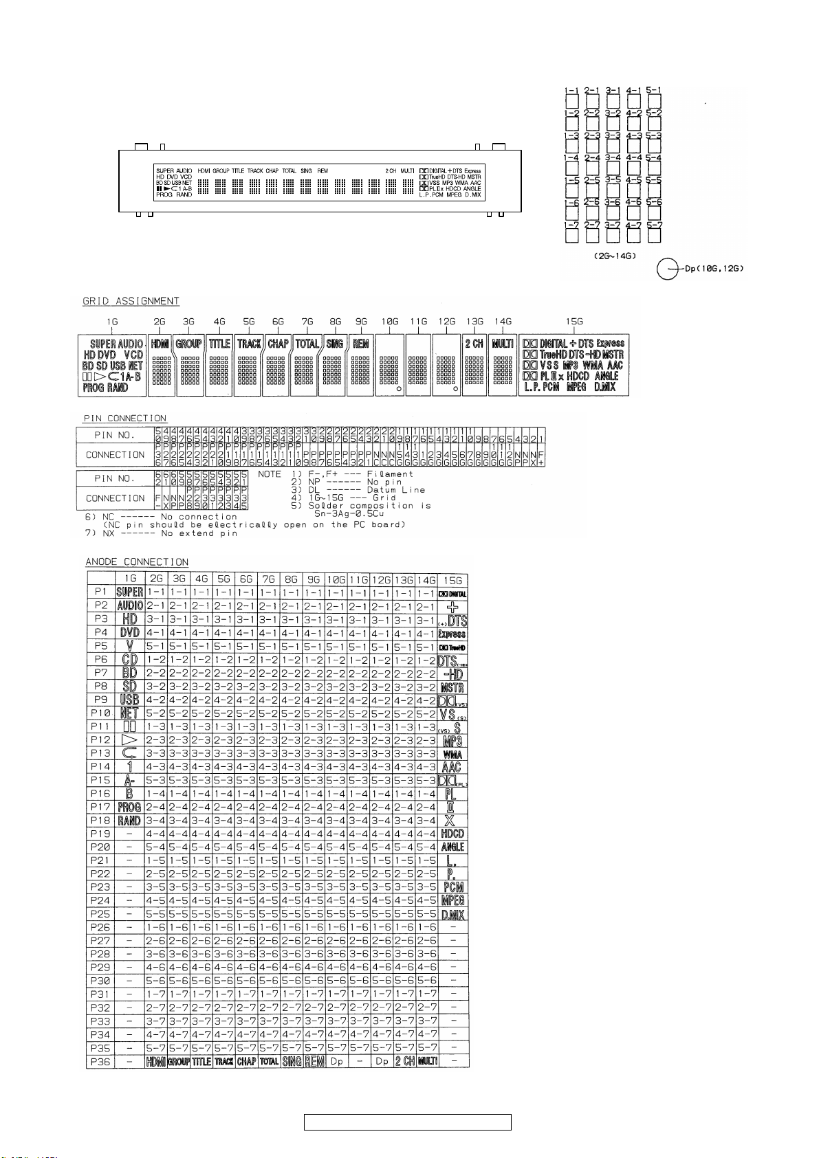
2. FL DISPLAY
FL TUBE (15-BT-114GNK) (8U-210089 : FL401)
50
DBP-4010UDCI/DBP-4010UD
Page 51

BLOCK DIAGRAM
t
[Dig
]
A
B
A
A
B
r
r
DENON
]
K
k
k
[
]
t
(
)
[
]
t
[
]
[
]
BD / DVD / CD
DRIVE UNIT
BD / DVD / CD
Mecha
Pick up
Spindle
Moto
Sled
(Steping)
Moto
tray
㪽㫉㫆㫄㩷㪧㪦㪮㪜㪩㩷㪪㪬㪧㪧㪣㪰㩷㪧㪮㪙
FAN
RS232C
REMORT IN
REMORT OUT
㪚㪰
㪚㪯
HIN202EIBNZ
to IR module
from system u-
POWER/INTERFACE SUPPLY PWB
POWER TRANS
㪚㪯 㪚㪯
㪚㪯
㪚㪯
SMPS(+12V)
Digtal SERVO
Decoder
[R8J32801AFPV]
FE
DRIVER
[BD7956FS]
watermark
AD8062ARMZ
SACD
DECODER
[CXD2753R]
[Bass Manager]
[Down Mix]
[LPF/HPF]
[CH Volume]
SYSTEM u-com Block
SYS u-com [R5F364VDNFB]
DC/DC(+5V)
[SI-8005Q-TL]
㪊㪊㪤
SATA Brige
S/ATAPI
watermark
EXPANDER
16M SDRAM
[M12L16161A -7TG]
FL DRV
IR/REMO
ON/ST
[BU19502KV-
SE2]
FE
BA6846FV
[XC3S500E-
4FTG256C
DSD
KEY CONT
BE CONT
REMO CONT
RS232C
㪉㪌㪤
[SN74CBTLV16210]
[SN74CBTLV16210]
[SN74CBTLV16212]
[W19B160BBT7]
P/ATAPI
㹤
Local SPI
FPGA
SPI
CEC
㪚㪯
㪚㪰
㪚㪯
㪚㪯
FE SACD PWB
Bus SW
F/E Block
16Mbits NOR
FLASH
㪊㪊㪤
SACD Bloc
SPI
FUN
POWER
㪚㪯
㫋㫆㩷㪤㪘㪠㪥㩷㪧㪮㪙
㫋㫆㩷㪝㪜㩷㪪㪘㪚㪛㩷㪧㪮㪙
㫋㫆㩷㪘㫅㪸㫃㫆㪾㩷㪘㪬㪛㪠㪦㩷㪧㪮㪙
㫋㫆㩷㪫㪩㪘㪥㪪㪝㪦㪩㪤㩷㪧㪮㪙
㪚㪯
㪚㪯
㪉㪇㪤
㪊㪊䌫
CEC
232C
MAIN PWB
㪚㪰
㫋㫆㩷㪪㪛㩷㪚㪘㪩㪛㩷㪧㪮㪙
MPEG DECORDER
[R8A34019EV01S]
P/ATAPI
FE CONT
AACS
CPPM
SPI
SPI SPI
㪚㪰
㪉㪎㪆㪉㪋㪆㪉㪉㪤
CLOCK GENERATE BLOCK
PLL1
PLL2
PLL4
XTAL
CLK SEL
VCXO
PLL
CLK GEN
232C
SELECTOR
SD CARD PWB
㪽㫉㫆㫄㩷㪤㪘㪠㪥㩷㪧㪮㪙
Etherne
nalog VIDEO PWB
㪚㪯
㪚㪯
㪚㪯
㪚㪯
HDMI
TX
[V1.3]
SiI9134
ital Audio Signal
VIDEO
ENCODER
ADV7340
VIDEO
ENCODER
ADV7340
㪚㪜㪚㩷㫋㫆㩷㫊㫐㫊㫋㪼㫄㩷㫌㪄㪺㫆㫄
Digital VIDEO Block
VIDEO
DRIVER
NJM2566AV
HDMI
connector
CVBS
COMPONENTOUT
CEC
SD
GUI
[Bass Management]
BD+
[HD Audio decode]
Re-Encode
[DD]
[DTS]
Ethernet
VIDEO CONT
CPRM
CLOSED
CAPTION
Ether
D.Video (HD)
D.Video (SD)
S/PDIF
RJ45
ETHER HUB
MII S(Y/C) OUT
SMSC
[LAN9313]
Pulse TRANS
DDR2
256M
SDRAM
Web Control
Bridge Co.
[DM860]
NAND
FLASH
Web Control Block
(COMPONENT / HDMI)
Digital Video Signal Interface
HD: 720p,50/60 1080i,50/60 1080p,24 TMDS
480p,60/576p,50 480i,60/576i/50
SD: 480i,60/576i,50
DDR2
I/P & Scaling
[ABT2015]
PLD
[EPM570
F256C5N]
B/E Block
PCM/RAW
[IIS]
IEC60938/61937
LPCM(DD/DTS) SPDIF OPT
LPCM(DD/DTS)
LPCM(down sample/down mix) COAX
Raw Data(DD+/D TrueHD/DTS-HD etc)
DSD LVDS DENON LINK
AUDIO SIGNAL
DSD/IIS/SPDIF SELECTOR
FPGA
512Mbits DDR2 SDRAM
[AD24 Multi]
[EP3C16F256C8N]
HDMI
SPDIF
LINK
DIR
[LC89057W-VF4A]
OPT
COAX
DENON
LIN
㪉㪋㪤
512Mbits DDR2 SDRAM
DIT
1Gbits DDR2 SDRAM
[AK4101AVQ]
PCM
㪉㪇㪤
DSD
Digital AUDIO Bloc
nalog AUDIO MIX PW
AUDIO DAC
PCM1796×2
㪚㪰
㪚㪯
OPAMP
nalog AUDIO Multi PW
AUDIO DAC
PCM1796×3
㪚㪰
OPAMP
Gain
con
㪚㪯
㪚㪯
Gain
con
㪽㫉㫆㫄㩷㪧㪦㪮㪜㪩㩷㪪㪬㪧㪧㪣㪰㩷㪧㪮㪙
CY
MUTE
MUTE
1Gbits DDR2 SDRAM
1Gbits DDR2 SDRAM
1Gbits DDR2 SDRAM
1Gbits NOR FLASH
16Mbits NOR FLASH
[W198160BBT7]
㪚㪰
㪽㫉㫆㫄㩷㪧㪦㪮㪜㪩㩷㪪㪬㪧㪧㪣㪰㩷㪧㪮㪙
SD CARD C , SW
CX
DISPLAY PWB
FL
TUBE
Button sw
FL
DRIVE
CX
CY
TRANSFORM PWB
IR
Module
STANDBY-SW PWB
Button sw
LED
CX
CY
CY
AUDIO DSP
[AL24 Multi]
[DSD/PCM Changer]
[Bass Management]
-
CY
㪧㪦㪮㪜㪩㩷㪪㪬㪧㪧㪣㪰㩷㪧㪮㪙
64Mbits SDRAM
[W9864G2GH-6]
㪽㫉㫆㫄
MIX L/R
F L/R
S L/R
SB L/R
51
DBP-4010UDCI/DBP-4010UD
Page 52

PRINTED WIRING BOARDS
8U-210086 A.AUDIO/VIDEO P.W.B. UNIT(1/2)
52
DBP-4010UDCI/DBP-4010UD
COMPONENT SIDE
Page 53
8U-210086 A.AUDIO/VIDEO P.W.B. UNIT(2/2)
53
DBP-4010UDCI/DBP-4010UD
FOIL SIDE
Page 54

8U-210089 POWER/DISPLAY P.W.B. UNIT(1/2)
54
DBP-4010UDCI/DBP-4010UD
COMPONENT SIDE
Page 55

8U-210089 POWER/DISPLAY P.W.B. UNIT(2/2)
55
DBP-4010UDCI/DBP-4010UD
FOIL SIDE
Page 56

8U-310041 MAIN P.W.B. UNIT(1/2)
56
DBP-4010UDCI/DBP-4010UD
COMPONENT SIDE
Page 57

8U-310041 MAIN P.W.B. UNIT(2/2)
57
DBP-4010UDCI/DBP-4010UD
FOIL SIDE
Page 58

8U-310037 FE/SACD P.W.B. UNIT
COMPONENT SIDE
FOIL SIDE
58
DBP-4010UDCI/DBP-4010UD
Page 59
NOTE FOR PARTS LIST
1.
Parts for which "nsp" is indicated on this table cannot be supplied.
When ordering of part, clearly indicate "1" and "I" (i) to avoid mis-supplying.
2.
Ordering part without stating its part number can not be supplied.
3.
Part indicated with the mark "★" is not illustrated in the exploded view.
4.
Not including General-purpose Carbon Film Resistor in the P.W.Board parts list. (Refer to the Schematic Diagram for those parts.)
5.
Not including General-purpose Carbon Chip Resistor in the P.W.Board parts list. (Refer to the Schematic Diagram for those parts.)
6.
WARNING:
Parts marked with this symbol z have critical characteristics.
Use ONLY replacement parts recommended by the manufacturer.
● Resistors
Ex.: RN
Type
RD : Carbon
RC : Composition
RS : Metal oxide film
RW: winding
RN : Metal film
RK : Metal mixture
* Resistance
2
14K
Shape
and performance
Indicates number of zeros after effective number.
2-digit effective number.
2E
Power
2B : 1/8 W
2E : 1/4 W
2H : 1/2 W
3A : 1 W
3D : 2 W
3F : 3 W
3H : 5 W
1800ohm=1.8kohm18
182
Resistance
F:±1%
G:±2%
J:±5%
K:±10%
M:±20%
G
Allowable
error
P : Pulse-resistant type
NL : Low noise type
NB : Non-burning type
FR : Fuse-resistor
F : Lead wire forming
FR
Others
: Units: ohm
● Capacitors
Ex.: CE
Type
CE : Aluminum foil
electrolytic
CA : Aluminium solid
electrolytic
CS : Tantalum electrolytic
CQ : Film
CK : Ceramic
CC : Ceramic
CP : Oil
CM: Mica
CF : Metallized
CH : Metallized
* Capacity (electrolyte only)
2
・ Units:μF.
1.2ohm1R 2
1-digit effective number.
2-digit effective number, decimal point indicated by R.
04W
Shape
and performance
Indicates number of zeros after effective number.
2-digit effective number.
2200μF22
1H
Dielectric
strength
0J : 6.3 V
1A : 10 V
1C : 16 V
1E : 25 V
1V : 35 V
1H : 50 V
2A : 100 V
2B : 125 V
2C : 160 V
2D : 200 V
2E : 250 V
2H : 500 V
2J : 630 V
3R2
CapacityMAllowable
error
F:±1%
G:±2%
J:±5%
K:±10%
M:±20%
Z:±80%
: - 20%
P : +100%
C:±0.25pF
D:±0.5pF
= : Others
Others
BP
HS : High stability type
BP : Non-polar type
HR : Ripple-resistant type
DL : For change and discharge
HF : For assuring high requency
U : UL part
C : CSA part
W : UL-CSA part
F : Lead wire forming
2
・ Units:μF.
2.2μF2R
1-digit effective number.
2-digit effective number, decimal point indicated by R
* Capacity (except electrolyte)
2
・ Units:pF
・ When the dielectric strength is indicated in AC,"AC" is included after the dieelectric strength value.
2200pF=0.0022μF22
Indicates number of zeros after efective number.
(More than 2)
2-digit effective number.
1
・ Units:pF
Indicates number of zeros after effective numver.
(0 or 1)
2-digit effective number.
59
DBP-4010UDCI/DBP-4010UD
220pF22
Page 60

PARTS LIST OF P.W.B. UNIT
* Parts for which "nsp" is indicated on this table cannot be supplied.
* The parts listed below are for maintenance only, might differ from the parts used in the unit in appearances or dimensions.
Note: The symbols in the column "Remarks" indicate the following destinations.
E3 : U.S.A. and Canada model E2 : Europe model E2R : Russia model
E1 : Asia model E1C : Chaina model
8U-210086A A.AUDIO/VIDEO PWB UNIT ASSY
Ref. No. Part No. Part Name Remarks Q'ty New
SEMICONDUCTORS GROUP
IC101 00D2623362903 PCM1796DBR
IC102,103 00D2630615902 BA15218F-DXE2 +C
IC105,106 00D2630615902 BA15218F-DXE2 +C
IC210 00D2631100063 KIA7809API-U/P
IC211 00D2631099048 KIA7909PI
IC214 00D2631262901 PST600C-T-G
IC301 00D2623362903 PCM1796DBR
IC302,303 00D2630615902 BA15218F-DXE2 +C
IC305,306 00D2630615902 BA15218F-DXE2 +C
IC401 00D2623362903 PCM1796DBR
IC402,403 00D2630615902 BA15218F-DXE2 +C
IC405,406 00D2630615902 BA15218F-DXE2 +C
IC601 00D2623362903 PCM1796DBR
IC602,603 00D2630615902 BA15218F-DXE2 +C
IC605,606 00D2630615902 BA15218F-DXE2 +C
IC801 00D2623362903 PCM1796DBR
IC802,803 00D2630615902 BA15218F-DXE2 +C
IC805,806 00D2630615902 BA15218F-DXE2 +C
IC808 236810058609S ADV7340BSTZ-3
IC809 00D2631273903 NJM2566AV
IC810 236810058609S ADV7340BSTZ-3
IC811,812 00D2631282907 BD7820FP-E2
TR101-105 00D2730460905 KTC2875-B-RTK/P
TR107,108 00D2730460905 KTC2875-B-RTK/P
TR110 00D2730460905 KTC2875-B-RTK/P
TR112 00D2690119901 DTA124EKT96(TAPE) +C
TR113 00D2690082902 DTC114EKT96 +C
TR115 00D2690119901 DTA124EKT96(TAPE) +C
TR116 00D2690082902 DTC114EKT96 +C
TR210 00D2730487904 2SC2412K_T146R
TR211 00D2690083901 DTA114EKT96 +C
TR212 00D2690119901 DTA124EKT96(TAPE) +C
TR213 00D2730487904 2SC2412K_T146R
TR214 00D2690119901 DTA124EKT96(TAPE) +C
TR215 00D2690082902 DTC114EKT96 +C
TR216 00D2720025907 2SB562(C)TF
TR217 00D2690082902 DTC114EKT96 +C
TR218 00D2740188905 2SD1858TV2(Q/R)
TR219 00D2690119901 DTA124EKT96(TAPE) +C
TR220 00D2690082902 DTC114EKT96 +C
TR301-305 00D2730460905 KTC2875-B-RTK/P
TR307,308 00D2730460905 KTC2875-B-RTK/P
TR310 00D2730460905 KTC2875-B-RTK/P
TR312 00D2690119901 DTA124EKT96(TAPE) +C
TR313 00D2690082902 DTC114EKT96 +C
TR315 00D2690119901 DTA124EKT96(TAPE) +C
TR316 00D2690082902 DTC114EKT96 +C
60
DBP-4010UDCI/DBP-4010UD
Page 61

Ref. No. Part No. Part Name Remarks Q'ty New
TR401-405 00D2730460905 KTC2875-B-RTK/P
TR407,408 00D2730460905 KTC2875-B-RTK/P
TR410 00D2730460905 KTC2875-B-RTK/P
TR412 00D2690119901 DTA124EKT96(TAPE) +C
TR413 00D2690082902 DTC114EKT96 +C
TR415 00D2690119901 DTA124EKT96(TAPE) +C
TR416 00D2690082902 DTC114EKT96 +C
TR601-605 00D2730460905 KTC2875-B-RTK/P
TR607,608 00D2730460905 KTC2875-B-RTK/P
TR610,611 00D2730460905 KTC2875-B-RTK/P
TR612 00D2690119901 DTA124EKT96(TAPE) +C
TR613 00D2690082902 DTC114EKT96 +C
TR615 00D2690119901 DTA124EKT96(TAPE) +C
TR616 00D2690082902 DTC114EKT96 +C
TR801-805 00D2730460905 KTC2875-B-RTK/P
TR807,808 00D2730460905 KTC2875-B-RTK/P
TR810 00D2730460905 KTC2875-B-RTK/P
TR812 00D2690119901 DTA124EKT96(TAPE) +C
TR813 00D2690082902 DTC114EKT96 +C
TR815 00D2690119901 DTA124EKT96(TAPE) +C
TR816 00D2690082902 DTC114EKT96 +C
TR822-824 00D2710293901 2SA1022-B +C
TR826,827 00D2710293901 2SA1022-B +C
TR950 00D2690119901 DTA124EKT96(TAPE) +C
TR951 00D2690082902 DTC114EKT96 +C
TR952 00D2690119901 DTA124EKT96(TAPE) +C
TR953 00D2690082902 DTC114EKT96 +C
D210 00D2760401905 1SS133T77 (TAPE)
D220 00D2760401905 1SS133T77 (TAPE)
D223,224 00D2760717903 1SS355 TE-17 +C
D801,802 00D2760794900 KDS160-RTK/P
RESISTORS GROUP
R111 00D2412467954 RD14B2E751JT(AMRS)
R112 00D2412467954 RD14B2E751JT(AMRS)
R139 00D2412467954 RD14B2E751JT(AMRS)
R140 00D2412467954 RD14B2E751JT(AMRS)
R168 00D2412466955 RD14B2E301JT(AMRS)
R169 00D2412466955 RD14B2E301JT(AMRS)
R175 00D2412466955 RD14B2E301JT(AMRS)
R178 00D2412466955 RD14B2E301JT(AMRS)
R194 00D2412466955 RD14B2E301JT(AMRS)
R195 00D2412466955 RD14B2E301JT(AMRS)
R196 00D2412466955 RD14B2E301JT(AMRS)
R197 00D2412466955 RD14B2E301JT(AMRS)
R225 00D2442052915 RS14B3A182JNBST(S)
R226 00D2442052915 RS14B3A182JNBST(S)
R227 00D2442052915 RS14B3A182JNBST(S)
R247 00D2442052986 RS14B3A751JNBST(S)
R248 00D2442052986 RS14B3A751JNBST(S)
R272 00D2442052915 RS14B3A182JNBST(S)
R273 00D2442052915 RS14B3A182JNBST(S)
R274 00D2442052915 RS14B3A182JNBST(S)
61
DBP-4010UDCI/DBP-4010UD
Page 62

Ref. No. Part No. Part Name Remarks Q'ty New
R275 00D2442052915 RS14B3A182JNBST(S)
R294 00D2442051974 RS14B3A102JNBST(S)
R295 00D2442051974 RS14B3A102JNBST(S)
R368 00D2412465985 RD14B2E151JT(AMRS)
R369 00D2412465985 RD14B2E151JT(AMRS)
R375 00D2412465985 RD14B2E151JT(AMRS)
R378 00D2412465985 RD14B2E151JT(AMRS)
R468 00D2412465985 RD14B2E151JT(AMRS)
R469 00D2412465985 RD14B2E151JT(AMRS)
R475 00D2412465985 RD14B2E151JT(AMRS)
R478 00D2412465985 RD14B2E151JT(AMRS)
R668 00D2412465985 RD14B2E151JT(AMRS)
R669 00D2412465985 RD14B2E151JT(AMRS)
R675 00D2412465985 RD14B2E151JT(AMRS)
R678 00D2412465985 RD14B2E151JT(AMRS)
R868 00D2412465985 RD14B2E151JT(AMRS)
R869 00D2412465985 RD14B2E151JT(AMRS)
R875 00D2412465985 RD14B2E151JT(AMRS)
R878 00D2412465985 RD14B2E151JT(AMRS)
RE921 00D2472032905 RM73B--750DT(1608)
RE923 00D2472032905 RM73B--750DT(1608)
RE925 00D2472032905 RM73B--750DT(1608)
RE927 00D2472032905 RM73B--750DT(1608)
RE929 00D2472032905 RM73B--750DT(1608)
RE931 00D2472032905 RM73B--750DT(1608)
CAPACITORS GROUP
C101 nsp CK73B1H103KT (1608) +1608
C102 nsp CC73CH1H101JT +1608
C103 nsp CC73CH1H101JT +1608
C104 nsp CC73CH1H101JT +1608
C105 nsp 0.01UF,J,M,50V
C107 00D2544574922 CE04W1H101MT(RA3)
C110 00D2544574922 CE04W1H101MT(RA3)
C112 00D2573023949 CF73=1C103JT(ECHUX)
C113 00D2544574919 CE04W1H470MT(RA3)
C114 00D2544574919 CE04W1H470MT(RA3)
C116 00D2544574922 CE04W1H101MT(RA3)
C120 nsp CK73F1E104ZT +1608
C121 nsp CK73F1E104ZT +1608
C123 nsp 0.001UF,J,M,50V
C124 nsp 0.001UF,J,M,50V
C126 nsp 0.0068UF,J,M,50V
C127 nsp 0.018UF,J,M,50V,D=10,N/IND(M)
C128 nsp 0.0022UF,J,M,50V
C129 nsp CK73F1E104ZT +1608
C131 nsp 0.0022UF,J,M,50V
C132 nsp CK73F1E104ZT +1608
C134 00D2543091901 CE04D1H220MBPT (RBD)
C135 nsp CC73CH1H100DT +1608
C142 00D2544579707 CE04W1H221MC(RA3)
C143 nsp 0.01UF,J,M,50V
C144 00D2544579707 CE04W1H221MC(RA3)
C145 nsp 0.01UF,J,M,50V
62
DBP-4010UDCI/DBP-4010UD
Page 63

Ref. No. Part No. Part Name Remarks Q'ty New
C150 nsp CK73F1E104ZT +1608
C151 nsp CK73F1E104ZT +1608
C152 nsp 0.001UF,J,M,50V
C153 nsp 0.001UF,J,M,50V
C156 nsp 0.0068UF,J,M,50V
C157 nsp 0.018UF,J,M,50V,D=10,N/IND(M)
C158 nsp 0.0022UF,J,M,50V
C159 nsp 0.0022UF,J,M,50V
C160 nsp CK73F1E104ZT +1608
C161 nsp CK73F1E104ZT +1608
C163 nsp CC73CH1H100DT +1608
C164 00D2543091901 CE04D1H220MBPT (RBD)
C180 nsp CK73F1E104ZT +1608
C181 nsp CK73F1E104ZT +1608
C182 nsp CK73F1E104ZT +1608
C183 nsp CK73F1E104ZT +1608
C193 nsp CK73F1E104ZT +1608
C194 nsp CK73F1E104ZT +1608
C195 nsp CK73F1E104ZT +1608
C196 nsp CK73F1E104ZT +1608
C210 00D2544574922 CE04W1H101MT(RA3)
C211 00D2544574922 CE04W1H101MT(RA3)
C214 nsp CK73F1E104ZT +1608
C215 00D2544574922 CE04W1H101MT(RA3)
C216 00D2544574922 CE04W1H101MT(RA3)
C217 nsp CK73F1E104ZT +1608
C232 00D2544578711 CE04W1C222MC(RA3)
C233 nsp CK73F1E104ZT +1608
C234 00D2544574922 CE04W1H101MT(RA3)
C235 nsp CK73F1E104ZT +1608
C236 00D2544574922 CE04W1H101MT(RA3)
C301 nsp CK73B1H103KT (1608) +1608
C302 nsp CC73CH1H101JT +1608
C303 nsp CC73CH1H101JT +1608
C304 nsp CC73CH1H101JT +1608
C305 nsp 0.01UF,J,M,50V
C307 00D2544574922 CE04W1H101MT(RA3)
C309 00D2573024964 CF73=1C104JT(ECHUX)
C310 00D2544574922 CE04W1H101MT(RA3)
C311 nsp CK73B1H103KT (1608) +1608
C312 nsp CK73B1E104KT +1608
C313 00D2544574922 CE04W1H101MT(RA3)
C314 00D2544574922 CE04W1H101MT(RA3)
C315 00D2573024964 CF73=1C104JT(ECHUX)
C316 00D2544574922 CE04W1H101MT(RA3)
C317 nsp CK73B1H103KT (1608) +1608
C320 nsp CK73F1E104ZT +1608
C321 nsp CK73F1E104ZT +1608
C323 00D2573018925 CF73=1H102JT(ECHUX)
C324 00D2573018925 CF73=1H102JT(ECHUX)
C326 00D2573019924 CF73=1H682JT(ECHUX)
C327 00D2573019979 CF73=1H183JT(ECHUX)
C328 00D2573018967 CF73=1H222JT(ECHUX)
C329 nsp CK73F1E104ZT +1608
C331 00D2573018967 CF73=1H222JT(ECHUX)
C332 nsp CK73F1E104ZT +1608
63
DBP-4010UDCI/DBP-4010UD
Page 64

Ref. No. Part No. Part Name Remarks Q'ty New
C334 00D2543091901 CE04D1H220MBPT (RBD)
C335 nsp CC73CH1H100DT +1608
C337 00D2544579707 CE04W1H221MC(RA3)
C338 00D2544579707 CE04W1H221MC(RA3)
C340 nsp CC73CH1H471JT +1608
C341 nsp CC73CH1H471JT +1608
C350 nsp CK73F1E104ZT +1608
C351 nsp CK73F1E104ZT +1608
C352 00D2573018925 CF73=1H102JT(ECHUX)
C353 00D2573018925 CF73=1H102JT(ECHUX)
C356 00D2573019924 CF73=1H682JT(ECHUX)
C357 00D2573019979 CF73=1H183JT(ECHUX)
C358 00D2573018967 CF73=1H222JT(ECHUX)
C359 00D2573018967 CF73=1H222JT(ECHUX)
C360 nsp CK73F1E104ZT +1608
C361 nsp CK73F1E104ZT +1608
C363 nsp CC73CH1H100DT +1608
C364 00D2543091901 CE04D1H220MBPT (RBD)
C380 nsp CK73F1E104ZT +1608
C381 nsp CK73F1E104ZT +1608
C382 nsp CK73F1E104ZT +1608
C383 nsp CK73F1E104ZT +1608
C401 nsp CK73B1H103KT (1608) +1608
C402 nsp CC73CH1H101JT +1608
C403 nsp CC73CH1H101JT +1608
C404 nsp CC73CH1H101JT +1608
C405 nsp 0.01UF,J,M,50V
C407 00D2544574922 CE04W1H101MT(RA3)
C409 00D2573024964 CF73=1C104JT(ECHUX)
C410 00D2544574922 CE04W1H101MT(RA3)
C411 nsp CK73B1H103KT (1608) +1608
C412 nsp CK73B1E104KT +1608
C413 00D2544574922 CE04W1H101MT(RA3)
C414 00D2544574922 CE04W1H101MT(RA3)
C415 00D2573024964 CF73=1C104JT(ECHUX)
C416 00D2544574922 CE04W1H101MT(RA3)
C417 nsp CK73B1H103KT (1608) +1608
C420 nsp CK73F1E104ZT +1608
C421 nsp CK73F1E104ZT +1608
C423 00D2573018925 CF73=1H102JT(ECHUX)
C424 00D2573018925 CF73=1H102JT(ECHUX)
C426 00D2573019924 CF73=1H682JT(ECHUX)
C427 00D2573019979 CF73=1H183JT(ECHUX)
C428 00D2573018967 CF73=1H222JT(ECHUX)
C429 nsp CK73B1E104KT +1608
C431 00D2573018967 CF73=1H222JT(ECHUX)
C432 nsp CK73B1E104KT +1608
C434 00D2543091901 CE04D1H220MBPT (RBD)
C435 nsp CC73CH1H100DT +1608
C437 00D2544579707 CE04W1H221MC(RA3)
C438 00D2544579707 CE04W1H221MC(RA3)
C440 nsp CC73CH1H471JT +1608
C441 nsp CC73CH1H471JT +1608
C450 nsp CK73F1E104ZT +1608
C451 nsp CK73F1E104ZT +1608
C452 00D2573018925 CF73=1H102JT(ECHUX)
64
DBP-4010UDCI/DBP-4010UD
Page 65

Ref. No. Part No. Part Name Remarks Q'ty New
C453 00D2573018925 CF73=1H102JT(ECHUX)
C456 00D2573019924 CF73=1H682JT(ECHUX)
C457 00D2573019979 CF73=1H183JT(ECHUX)
C458 00D2573018967 CF73=1H222JT(ECHUX)
C459 00D2573018967 CF73=1H222JT(ECHUX)
C460 nsp CK73B1E104KT +1608
C461 nsp CK73B1E104KT +1608
C463 nsp CC73CH1H100DT +1608
C464 00D2543091901 CE04D1H220MBPT (RBD)
C467 nsp CK73F1E104ZT +1608
C478 nsp CK73F1E104ZT +1608
C479 nsp CK73F1E104ZT +1608
C601 nsp CK73B1H103KT (1608) +1608
C602 nsp CC73CH1H101JT +1608
C603 nsp CC73CH1H101JT +1608
C604 nsp CC73CH1H101JT +1608
C605 nsp 0.01UF,J,M,50V
C607 00D2544574922 CE04W1H101MT(RA3)
C609 00D2573024964 CF73=1C104JT(ECHUX)
C610 00D2544574922 CE04W1H101MT(RA3)
C611 nsp CK73B1H103KT (1608) +1608
C612 nsp CK73B1E104KT +1608
C613 00D2544574922 CE04W1H101MT(RA3)
C614 00D2544574922 CE04W1H101MT(RA3)
C615 00D2573024964 CF73=1C104JT(ECHUX)
C616 00D2544574922 CE04W1H101MT(RA3)
C617 nsp CK73B1H103KT (1608) +1608
C620 nsp CK73F1E104ZT +1608
C621 nsp CK73F1E104ZT +1608
C623 00D2573018925 CF73=1H102JT(ECHUX)
C624 00D2573018925 CF73=1H102JT(ECHUX)
C626 00D2573019924 CF73=1H682JT(ECHUX)
C627 00D2573019979 CF73=1H183JT(ECHUX)
C628 00D2573018967 CF73=1H222JT(ECHUX)
C629 nsp CK73B1E104KT +1608
C631 00D2573018967 CF73=1H222JT(ECHUX)
C632 nsp CK73B1E104KT +1608
C634 00D2543091901 CE04D1H220MBPT (RBD)
C635 nsp CC73CH1H100DT +1608
C637 00D2544579707 CE04W1H221MC(RA3)
C638 00D2544579707 CE04W1H221MC(RA3)
C640 nsp CC73CH1H471JT +1608
C641 nsp CC73CH1H471JT +1608
C650 nsp CK73F1E104ZT +1608
C651 nsp CK73F1E104ZT +1608
C652 00D2573018925 CF73=1H102JT(ECHUX)
C653 00D2573018925 CF73=1H102JT(ECHUX)
C656 00D2573019924 CF73=1H682JT(ECHUX)
C657 00D2573019979 CF73=1H183JT(ECHUX)
C658 00D2573018967 CF73=1H222JT(ECHUX)
C659 00D2573018967 CF73=1H222JT(ECHUX)
C660 nsp CK73B1E104KT +1608
C661 nsp CK73B1E104KT +1608
C663 nsp CC73CH1H100DT +1608
C664 00D2543091901 CE04D1H220MBPT (RBD)
C666 00D2543091901 CE04D1H220MBPT (RBD)
65
DBP-4010UDCI/DBP-4010UD
Page 66

Ref. No. Part No. Part Name Remarks Q'ty New
C667 nsp CK73F1E104ZT +1608
C668 nsp CK73F1E104ZT +1608
C669 nsp CK73F1E104ZT +1608
C801 nsp CK73B1H103KT (1608) +1608
C802 nsp CC73CH1H101JT +1608
C803 nsp CC73CH1H101JT +1608
C804 nsp CC73CH1H101JT +1608
C805 nsp 0.01UF,J,M,50V
C807 00D2544574922 CE04W1H101MT(RA3)
C809 00D2573024964 CF73=1C104JT(ECHUX)
C810 00D2544574922 CE04W1H101MT(RA3)
C811 nsp CK73B1H103KT (1608) +1608
C812 nsp CK73B1E104KT +1608
C813 00D2544574922 CE04W1H101MT(RA3)
C814 00D2544574922 CE04W1H101MT(RA3)
C815 00D2573024964 CF73=1C104JT(ECHUX)
C816 00D2544574922 CE04W1H101MT(RA3)
C817 nsp CK73B1H103KT (1608) +1608
C820 nsp CK73F1E104ZT +1608
C821 nsp CK73F1E104ZT +1608
C823 00D2573018925 CF73=1H102JT(ECHUX)
C824 00D2573018925 CF73=1H102JT(ECHUX)
C826 00D2573019924 CF73=1H682JT(ECHUX)
C827 00D2573019979 CF73=1H183JT(ECHUX)
C828 00D2573018967 CF73=1H222JT(ECHUX)
C829 nsp CK73B1E104KT +1608
C831 00D2573018967 CF73=1H222JT(ECHUX)
C832 nsp CK73B1E104KT +1608
C834 00D2543091901 CE04D1H220MBPT (RBD)
C835 nsp CC73CH1H100DT +1608
C837 00D2544579707 CE04W1H221MC(RA3)
C838 00D2544579707 CE04W1H221MC(RA3)
C840 nsp CC73CH1H471JT +1608
C841 nsp CC73CH1H471JT +1608
C850 nsp CK73F1E104ZT +1608
C851 nsp CK73F1E104ZT +1608
C852 00D2573018925 CF73=1H102JT(ECHUX)
C853 00D2573018925 CF73=1H102JT(ECHUX)
C856 00D2573019924 CF73=1H682JT(ECHUX)
C857 00D2573019979 CF73=1H183JT(ECHUX)
C858 00D2573018967 CF73=1H222JT(ECHUX)
C859 00D2573018967 CF73=1H222JT(ECHUX)
C860 nsp CK73B1E104KT +1608
C861 nsp CK73B1E104KT +1608
C863 nsp CC73CH1H100DT +1608
C864 00D2543091901 CE04D1H220MBPT (RBD)
C867 nsp CK73F1E104ZT +1608
C868 nsp CK73F1E104ZT +1608
C869 nsp CK73F1E104ZT +1608
C938 nsp CK73F1E104ZT +1608
C939 nsp CK73F1E104ZT +1608
C940 nsp CK73F1E104ZT +1608
C941 nsp CK73F1E104ZT +1608
C942 nsp CK73F1E104ZT +1608
C943 nsp CK73F1E104ZT +1608
C944 nsp CK73F1E104ZT +1608
66
DBP-4010UDCI/DBP-4010UD
Page 67

Ref. No. Part No. Part Name Remarks Q'ty New
C945 nsp CK73F1E104ZT +1608
C950 00D2544574922 CE04W1H101MT(RA3)
C951 00D2544574922 CE04W1H101MT(RA3)
C954 00D2544574922 CE04W1H101MT(RA3)
C957 00D2544574922 CE04W1H101MT(RA3)
CC240 00D2570038908 CK73B1A106KT +2125
CC241 nsp CK73B1E103KT(1005)
CC242 nsp CK73B1H102KT +1005
CC243 nsp CK73B1H102KT +1005
CC244 nsp CK73B1A104KT +1005
CC245 00D2570038908 CK73B1A106KT +2125
CC246 nsp CK73B1E103KT(1005)
CC249 00D2570038908 CK73B1A106KT +2125
CC250 00D2575006993 CK73B1H102KT +1005
CC251 nsp CK73B1A104KT +1005
CC252 nsp CK73B1A104KT +1005
CC254 nsp CK73B1H123KT +1608
CC255 nsp CK73B1A104KT +1005
CC256 nsp CK73B1A154KT +1608
CC257 nsp CK73B1H102KT +1005
CC258 nsp CK73B1A104KT +1005
CC259 nsp CK73B1H102KT +1005
CC260 00D2570038908 CK73B1A106KT +2125
CC261 nsp CK73B1A104KT +1005
CC262 nsp CK73B1E103KT(1005)
CC263 nsp CK73B1E103KT(1005)
CC264 nsp CK73B1E103KT(1005)
CC265 00D2570038908 CK73B1A106KT +2125
CC266 nsp CK73B1E103KT(1005)
CC267 nsp CK73B1A104KT +1005
CC268 nsp CK73B1H102KT +1005
CC269 nsp CK73B1H123KT +1608
CC270 nsp CK73B1A154KT +1608
CC271 nsp CK73B1H102KT +1005
CC272 nsp CK73B1A104KT +1005
CC273 nsp CK73B1A104KT +1005
CC274 00D2570038908 CK73B1A106KT +2125
CC275 nsp CK73B1A104KT +1005
CC276 nsp CK73B1H102KT +1005
CC277 nsp CK73B1H102KT +1005
CC278 nsp CK73B1A104KT +1005
CC279 nsp CK73B1E103KT(1005)
CC283 nsp CK73B1A104KT +1005
CC284 nsp CK73B1A104KT +1005
CC285 nsp CK73B1A104KT +1005
CC288 00D2570525903 CK73B0J475KT(P) +1608
CC289 nsp CK73B1H102KT +1005
CC290 00D2572018900 CS77B1A100MT(NOJ)
CC291 00D2572018900 CS77B1A100MT(NOJ)
CC292 nsp CK73B1A104KT +1005
CC801 00D2570038908 CK73B1A106KT +2125
CC802 nsp CK73B1E103KT(1005)
CC803 nsp CK73B1H102KT +1005
CC804 nsp CK73B1H102KT +1005
CC805 nsp CK73B1A104KT +1005
67
DBP-4010UDCI/DBP-4010UD
Page 68

Ref. No. Part No. Part Name Remarks Q'ty New
CC806 00D2570038908 CK73B1A106KT +2125
CC807 nsp CK73B1E103KT(1005)
CC811 nsp CK73B1H123KT +1608
CC812 nsp CK73B1A154KT +1608
CC814 nsp CK73B1A104KT +1005
CC815 nsp CK73B1H102KT +1005
CC816 00D2570038908 CK73B1A106KT +2125
CC817 nsp CK73B1E103KT(1005)
CC818 nsp CK73B1E103KT(1005)
CC819 nsp CK73B1E103KT(1005)
CC820 nsp CK73B1E103KT(1005)
CC821 nsp CK73B1A104KT +1005
CC822 nsp CK73B1H123KT +1608
CC823 nsp CK73B1A154KT +1608
CC824 00D2570038908 CK73B1A106KT +2125
CC825 nsp CK73B1A104KT +1005
CC826 nsp CK73B1H102KT +1005
CC829 nsp CK73B1A104KT +1005
CC830 nsp CK73B1A104KT +1005
CC831 00D2570525903 CK73B0J475KT(P) +1608
CC832 nsp CK73B1A104KT +1005
CC833 00D2572018900 CS77B1A100MT(NOJ)
CC834 00D2572018900 CS77B1A100MT(NOJ)
CC835 nsp CK73B1A104KT +1005
CC850 nsp CK73B1A104KT +1005
CC851 00D2570038908 CK73B1A106KT +2125
CC852 00D2570038908 CK73B1A106KT +2125
CC853 00D2570038908 CK73B1A106KT +2125
CC854 00D2570038908 CK73B1A106KT +2125
CC856 00D2572018900 CS77B1A100MT(NOJ)
CC857 nsp CK73B1A104KT +1005
CC858 nsp CK73B1E103KT(1005)
CC859 nsp CK73B1A104KT +1005
CC860 nsp CK73B1A104KT +1005
CC861 nsp CK73B1A104KT +1005
CC862 nsp CK73B1A104KT +1005
CC863 nsp CK73B1A104KT +1005
CC971 nsp RM73B--0R0KT +1608
CC972 nsp RM73B--0R0KT +1608
CC973 nsp RM73B--0R0KT +1608
CC975 00D2544533950 CE04W0J471MT SMG/RE3
CC977 nsp RM73B--0R0KT +1608
CC978 nsp RM73B--0R0KT +1608
CC979 nsp RM73B--0R0KT +1608
CC980 00D2544533950 CE04W0J471MT SMG/RE3
CC982 00D2544533950 CE04W0J471MT SMG/RE3
CC984 00D2544533950 CE04W0J471MT SMG/RE3
CC986 00D2544533950 CE04W0J471MT SMG/RE3
OTHERS PARTS GROUP
CX155 nsp 15P FFC BASE SIDE(P=0.5MM)
CX181 nsp 18P CON.SOCKET TUC-P
CX182 nsp 18P CON.SOCKET TUC-P
CX505 nsp 50FY-BMT-TB(LF)(SN)
DBP-4010UDCI/DBP-4010UD
68
Page 69

Ref. No. Part No. Part Name Remarks Q'ty New
CY031 nsp 3P CONN.BASE(KR-PH)
CY041 nsp B4PS-VH
CY181 nsp 18P CON.BASE TUC-P
CY182 nsp 18P CON.BASE TUC-P
CY331 nsp JACK 33FMN-BTK-A
CY332 nsp JACK 33FMN-BTK-A
FB802 00D2350136907 FBMJ1608HS280NT +1608
FB803 00D2350136907 FBMJ1608HS280NT +1608
FB804 00D2350136907 FBMJ1608HS280NT +1608
FB805 00D2350136907 FBMJ1608HS280NT +1608
FB811 00D2350136907 FBMJ1608HS280NT +1608
FB812 00D2350136907 FBMJ1608HS280NT +1608
FB813 00D2350136907 FBMJ1608HS280NT +1608
FB814 00D2350136907 FBMJ1608HS280NT +1608
FB889 00D2350136907 FBMJ1608HS280NT +1608
FB899 00D2350136907 FBMJ1608HS280NT +1608
JK101 00D2048728009 1P PIN JACK(BK)-LF
JK102 00D2048728009 1P PIN JACK(BK)-LF
JK301 00D2048728009 1P PIN JACK(BK)-LF
JK302 00D2048728009 1P PIN JACK(BK)-LF
JK401 00D2048728009 1P PIN JACK(BK)-LF
JK402 00D2048728009 1P PIN JACK(BK)-LF
JK601 00D2048728009 1P PIN JACK(BK)-LF
JK602 00D2048728009 1P PIN JACK(BK)-LF
JK801 00D2048728009 1P PIN JACK(BK)-LF
JK802 00D2048728009 1P PIN JACK(BK)-LF
JK901 00D2048728009 1P PIN JACK(BK)-LF
JK902 00D2048728009 1P PIN JACK(BK)-LF
JK903 00D2048728009 1P PIN JACK(BK)-LF
JK904 00D2048728009 1P PIN JACK(BK)-LF
JK905 00D2051395005 1P S-TERMINAL-LF
L803 00D2350125905 INDUCTOR(FLC32C220K)+3216
L806 00D2350125905 INDUCTOR(FLC32C220K)+3216
L901 00D2350125905 INDUCTOR(FLC32C220K)+3216
ST201 nsp STYLE PIN
ST901 nsp STYLE PIN
W912 nsp M3 SCREW TERMINAL
W913 nsp M3 SCREW TERMINAL
RS301 00D2473010900 RM73B--472JT+1005
RS303 00D2473001906 RM73B--0R0KT+1005
RS304 00D2473001906 RM73B--0R0KT+1005
RS305 00D2473001906 RM73B--0R0KT+1005
RS306 00D2472042937 RM73B--153DT(1608)
RS307 00D2472036943 RM73B--273DT(1608)
RS308 00D2472036956 RM73B--303DT(1608)
RS309 00D2473010984 RM73B--103JT +1005
RS312 00D2473007926 RM73B--331JT
RS313 nsp RM73B--0R0KT +1608
RS314 nsp RM73B--0R0KT +1608
RS315 nsp RM73B--0R0KT +1608
69
DBP-4010UDCI/DBP-4010UD
Page 70

Ref. No. Part No. Part Name Remarks Q'ty New
RS316 nsp RM73B--0R0KT +1608
RS317 nsp RM73B--0R0KT +1608
RS318 nsp RM73B--0R0KT +1608
RS319 nsp RM73B--0R0KT +1608
RS320 nsp RM73B--0R0KT +1608
RS321 nsp RM73B--0R0KT +1608
RS322 nsp RM73B--0R0KT +1608
RS324 00D2473007926 RM73B--331JT
RS326 nsp RM73B--0R0KT +1608
RS327 00D2473010900 RM73B--472JT+1005
RS328 00D2472034903 RM73B--511DT(1608)
RS331 00D2473001906 RM73B--0R0KT+1005
RS332 00D2473001906 RM73B--0R0KT+1005
RS333 00D2473001906 RM73B--0R0KT+1005
RS334 00D2473001906 RM73B--0R0KT+1005
RS335 00D2473001906 RM73B--0R0KT+1005
RS336 00D2473001906 RM73B--0R0KT+1005
RS338 00D2472036914 RM73B--203DT(1608)
RS339 00D2472037968 RM73B--823DT(1608)
RS340 00D2473007926 RM73B--331JT
RS342 00D2472036956 RM73B--303DT(1608)
RS343 00D2472005987 RM73B--221JT +1608
RS344 00D2472005987 RM73B--221JT +1608
RS345 00D2472005987 RM73B--221JT +1608
RS346 00D2473007926 RM73B--331JT
RS347 nsp RM73B--0R0KT +1608
RS348 00D2472032905 RM73B--750DT(1608)
RS349 nsp RM73B--0R0KT +1608
RS350 00D2472032905 RM73B--750DT(1608)
RS351 nsp RM73B--0R0KT +1608
RS352 00D2472032905 RM73B--750DT(1608)
RS353 00D2472032905 RM73B--750DT(1608)
RS354 00D2472032905 RM73B--750DT(1608)
RS355 00D2472032905 RM73B--750DT(1608)
RS356 00D2472003989 RM73B--330JT +1608
RS357 00D2472003989 RM73B--330JT +1608
RS358 00D2472003989 RM73B--330JT +1608
RS359 00D2472007985 RM73B--152JT +1608
RS360 00D2472007985 RM73B--152JT +1608
RS361 00D2472007985 RM73B--152JT +1608
RS365 nsp RM73B--0R0KT +1608
RS366 nsp RM73B--0R0KT +1608
RS367 nsp RM73B--0R0KT +1608
RS370 00D2473001906 RM73B--0R0KT+1005
RS371 00D2473001906 RM73B--0R0KT+1005
RS372 00D2473001906 RM73B--0R0KT+1005
RS401 00D2473001906 RM73B--0R0KT+1005
RS402 00D2473001906 RM73B--0R0KT+1005
RS404 00D2473010900 RM73B--472JT+1005
RS406 00D2473001906 RM73B--0R0KT+1005
RS407 00D2473001906 RM73B--0R0KT+1005
RS408 00D2473001906 RM73B--0R0KT+1005
RS409 00D2473001906 RM73B--0R0KT+1005
RS412 00D2473007926 RM73B--331JT
RS413 nsp RM73B--0R0KT +1608
RS414 nsp RM73B--0R0KT +1608
70
DBP-4010UDCI/DBP-4010UD
Page 71

Ref. No. Part No. Part Name Remarks Q'ty New
RS415 nsp RM73B--0R0KT +1608
RS416 nsp RM73B--0R0KT +1608
RS417 nsp RM73B--0R0KT +1608
RS418 nsp RM73B--0R0KT +1608
RS419 nsp RM73B--0R0KT +1608
RS420 nsp RM73B--0R0KT +1608
RS421 nsp RM73B--0R0KT +1608
RS422 nsp RM73B--0R0KT +1608
RS423 00D2473007926 RM73B--331JT
RS425 00D2472041925 RM73B--472DT(1608)
RS426 nsp RM73B--0R0KT +1608
RS427 00D2472036969 RM73B--333DT(1608)
RS428 00D2472006973 RM73B--511JT +1608
RS431 00D2473006985 RM73B--221JT +1005
RS432 00D2473006985 RM73B--221JT +1005
RS433 00D2473006985 RM73B--221JT +1005
RS434 00D2472005987 RM73B--221JT +1608
RS435 00D2473001906 RM73B--0R0KT+1005
RS436 00D2473001906 RM73B--0R0KT+1005
RS438 00D2473007926 RM73B--331JT
RS439 00D2473007926 RM73B--331JT
RS440 nsp RM73B--0R0KT +1608
RS441 00D2472033946 RM73B--301DT(1608)
RS442 nsp RM73B--0R0KT +1608
RS443 00D2472033946 RM73B--301DT(1608)
RS446 00D2472003989 RM73B--330JT +1608
RS447 00D2472003989 RM73B--330JT +1608
RS448 00D2472007985 RM73B--152JT +1608
RS449 00D2472007985 RM73B--152JT +1608
RS452 nsp RM73B--0R0KT +1608
RS453 nsp RM73B--0R0KT +1608
RS457 00D2473001906 RM73B--0R0KT+1005
RS458 00D2473001906 RM73B--0R0KT+1005
nsp 1P L=55mm UL1007 AWG22
BKE3: ~ Lot No.629
BKE2: ~ Lot No.100
SPE2: ~ Lot No.230
SPE1: ~ Lot No.100
SPE1C: ~ Lot No.30
BKE2R: ~ Lot No.30
71
DBP-4010UDCI/DBP-4010UD
Page 72

8U-210089A POWER/DISPLAY PWB UNIT ASSY(E3 model)
8U-210089C POWER/DISPLAY PWB UNIT ASSY(E2, E2R, E1, E1C model)
Ref. No. Part No. Part Name Remarks Q'ty New
SEMICONDUCTORS GROUP
z IC102 231010077702S STR-Y6453 E3 *
z IC102 231010077719S STR-Y6473 E2,E2R,E1,E1C *
z IC103 00D2623047008 PC123Y22
IC105 231810041507S SI-8005Q-TL
IC401 00D2623606902 PT6302-R-001(L)
IC402 00D2623602003 GP1UE271XKVF
IC403 00D2623571901 HIN202EIBNZ-T
TR102 00D2730464901 KTC3875S-GR-RTK/P
TR103 00D2720025907 2SB562(C)TF
TR104 00D2690082902 DTC114EKT96 +C E3
TR105 00D2730468907 KTC3199-GR-AT/P
TR106 00D2690192902 KRC102S-RTK/P (10K-10K)
TR110 00D2730464901 KTC3875S-GR-RTK/P
TR304 00D2740188905 2SD1858TV2(Q/R)
TR401 00D2730464901 KTC3875S-GR-RTK/P
TR402 00D2690191903 KRA104S-RTK/P (47K-47K)
TR403 00D2720160901 2SB1132T100Q +C
TR404 00D2690054901 DTC144EKT96 +C
TR405-407 00D2690082902 DTC114EKT96 +C
TR409 00D2690192902 KRC102S-RTK/P (10K-10K)
TR410,411 00D2710312905 KTA1504S-GR-RTK/P
TR412 00D2690193901 KRC104S-RTK/P (47K-47K)
z D101 00D2760767005 RBV-406
D102 00D2760727919 AL01ZT (WK)
z D103 00D2760758001 SARS03
D104 00D2760727919 AL01ZT (WK)
D105 00D2760787001 RN2Z
D106 00D2760727919 AL01ZT (WK)
D107 204050011708S FME-210B
D108-113 00D2760750902 RB521S-30TE61 +REF
D115 00D2760401905 1SS133T77 (TAPE)
D117 00MHD20002711 1D3 1A/200V
D118 00D2760401905 1SS133T77 (TAPE)
D124 203850012502S SJPB-L4
D302 00D2760794900 KDS160-RTK/P
D402-404 00D2760717903 1SS355 TE-17 +C
D405 00D2760750902 RB521S-30TE61 +REF
D406,407 00D2760794900 KDS160-RTK/P
ZD101 00D2760761959 MTZJ15B T77 E3
ZD102 00D2760636903 MTZJ8.2BT77
ZD103 00D2631185907 TL431ACLP
ZD104 00D2760665903 MTZJ16B T77
ZD105 00D2760760905 MTZJ3.6B T77
ZD107 00D2760665903 MTZJ16B T77
ZD302 00D2760761904 MTZJ9.1B T77
ZD405 00D2760760963 MTZJ6.2B T77
LD401-403 176010002405S LED (SLR343BC7T)
LD404 00D3939671002 SMLU12416W-S
LD405 263010032409S SIR-341STA49
DBP-4010UDCI/DBP-4010UD
72
Page 73

Ref. No. Part No. Part Name Remarks Q'ty New
z TH101 00D2790044002 NTH11D8R0LA
FL401 00D3938098000 FL TUBE(15-BT-114GNK)
RESISTORS GROUP
R101,102 129550003504S RM73B2E115JT(HV732B)
R104 00D2432094064 RW99=3DR33JF E3
R104 00D2432094077 RW99=3DR47JF E2,E2R,E1,E1C
R108 00D2442675716 RS14B3D683JNBF (ERG)
R115 00D2472035986 RM73B--332DT(1608)
R116 00D2472042911 RM73B--123DT(1608)
R120 00D2472034916 RM73B--561DT(1608)
R130 00D2472041925 RM73B--472DT(1608)
R134 00D2472035986 RM73B--332DT(1608)
R135 00D2472036985 RM73B--393DT(1608)
R142 00D2472036930 RM73B--243DT(1608)
R143 00D2472041925 RM73B--472DT(1608)
CAPACITORS GROUP
C101,102 132350030504S CK73B1C225KT 1608
C106 nsp CK73B1H103KT (1608) +1608
C107 nsp CK73B1H102KT +1608
C108 nsp CC73CH1H101JT +1608
C109 nsp CK73B1H103KT (1608) +1608
C110 nsp CK73B1H102KT +1608
C111 nsp CC73CH1H101JT +1608
C112 nsp CK73B1H103KT (1608) +1608
C113 nsp CK73B1H102KT +1608
C114 nsp CC73CH1H101JT +1608
C115,116 nsp RM73B--0R0KT +1608
C117 00D2544722949 CE04W1H010MT(GR)
z C118 00D2568039029 CF99--2EAC334K(LEMX)
z C119,120 00D2538035710 CK45E2EAC222MC(KY)
C121 nsp CK73B1H103KT (1608) +1608
C122 nsp CC73CH1H101JT +1608
C123 nsp CK73B1H102KT +1608
z C124 00D2538035710 CK45E2EAC222MC(KY)
z C126 00D2568039029 CF99--2EAC334K(LEMX)
z C128 00D2538029713 CK45F2EAC471KC(KX)
z C131 134010168202S CE68W2D331M Q25(KMM) E3
z C131 134010168226S CE68W2G121M Q25(KMM) E2,E2R,E1,E1C
C132 132050024205S CK45B3D102KC(DEHR) E3
C132 132050023202S CK45B3D471KC(DEHR) E2,E2R,E1,E1C
C134 nsp CK73B1A224KT +1608
C135 134050069402S CE04W2A270MT HB5(KY)
C137 00D2544524972 CE04W1H4R7MT SMG/RE3
C139,140 132510036571S CK73B2J153KT(3216)
C141 nsp CK73B1H472KT +1608
z C142 00D2538029700 CK45F2EAC222MC (KX)
C143 nsp CK73F1E104ZT +1608
C144,145 nsp CK73B1E223KT +1608
C146 134050090208S CE04W1C102MC J20(KY) *
C147 134050069402S CE04W2A270MT HB5(KY)
C148 00D2544711918 CE04W1A221MT F11(KY)
73
DBP-4010UDCI/DBP-4010UD
Page 74

Ref. No. Part No. Part Name Remarks Q'ty New
C149 00D2534548706 CC45R3A102KC
C150 00D2544806700 CE04W1C222MC K25(KY)
C151 00D2570517908 CK73B1C473KT +1608
C152 132350030504S CK73B1C225KT 1608
C153-156 nsp CK73B1H103KT (1608) +1608
C157 132350030504S CK73B1C225KT 1608
C158 nsp CK73B1H102KT +1608
C159 00D2544806700 CE04W1C222MC K25(KY)
C160 00D2544755903 CE04W1H560MT(KY)
C161 132350030504S CK73B1C225KT 1608
C162 00D2544806700 CE04W1C222MC K25(KY)
C163 132350030504S CK73B1C225KT 1608
C164 nsp CK73F1E104ZT +1608
C165 132350030504S CK73B1C225KT 1608
C166,167 nsp CK73B1H102KT +1608
C169 nsp CK73B1H102KT +1608
C170 134050090208S CE04W1C102MC J20(KY) *
C171 132350030504S CK73B1C225KT 1608
C173 nsp CK73B1H102KT +1608
C174 00D2544717925 CE04W1A101MT(GR)
C175,176 132350036502S CK73R1H104KT (1608)
C177 nsp CK73B1H102KT +1608
C178 134050090208S CE04W1C102MC J20(KY) *
C179 132350030504S CK73B1C225KT 1608
C180 nsp CK73F1E104ZT +1608
C182 132350036502S CK73R1H104KT (1608)
C183 nsp CK73B1H103KT (1608) +1608
C184,185 nsp CK73B1H102KT +1608
C186,187 nsp CK73B1H103KT (1608) +1608
C188 nsp CK73B1H102KT +1608
C190 nsp CK73F1E104ZT +1608
C191 nsp CK73B1H102KT +1608
C192 00MDF15103351 0.01UF,J,M,50V
C193 00MDF15221351 0.00022UF J M 50V
C194 nsp CK73B1H103KT (1608) +1608
C195 nsp CK73B1H102KT +1608
C196 nsp CK73B1H103KT (1608) +1608
C197 nsp CK73B1H102KT +1608
C198 nsp CK73B1H103KT (1608) +1608
C199 nsp CK73B1H102KT +1608
C200 00MDF15103351 0.01UF,J,M,50V
C201 00MDF15221351 0.00022UF J M 50V
C202 nsp CK73B1H103KT (1608) +1608
C203 nsp CK73B1H102KT +1608
C204 nsp CK73B1H103KT (1608) +1608
C205 nsp CK73B1H102KT +1608
C206-209 00D2544693939 CE04W1H101MT(RF0)
C211 132350030504S CK73B1C225KT 1608
z C213 00D2538026703 CK45E2EAC472MC
C272 nsp CK73B1H222KT +1608
C277 00MDK2647601Y GRM32EB31C476KE15L
C278 132350030504S CK73B1C225KT 1608
C301 nsp CK73F1E104ZT +1608
C302 nsp CK73B1H103KT (1608) +1608
C303-305 nsp CK73F1E104ZT +1608
C308 00D2544718937 CE04W1C470MT(GR)
74
DBP-4010UDCI/DBP-4010UD
Page 75

Ref. No. Part No. Part Name Remarks Q'ty New
C309 nsp CK73B1H103KT (1608) +1608
C310 nsp CK73B1H102KT +1608
C311 nsp CC73CH1H101JT +1608
C401,402 nsp CK73F1E104ZT +1608
C403 nsp CC73CH1H390JT +1608
C404 nsp CK73B1H103KT (1608) +1608
C405 00D2544213937 CE04W0J101MT (SRA)
C415 nsp CK73F1E104ZT +1608
C416 00D2544213924 CE04W0J470MT (SRA)
C417 nsp CK73F1E104ZT +1608
C419 nsp CK73F1E104ZT +1608
C431 nsp CK73B1H103KT (1608) +1608
C438-440 nsp CK73B1H103KT (1608) +1608
C443,444 nsp RM73B--0R0KT +1608
C445,446 nsp CC73CH1H101JT +1608
C447 nsp RM73B--0R0KT +1608
C449 nsp CK73B1H102KT +1608
C450,451 nsp CK73F1E104ZT +1608
C453-456 00D2544722907 CE04W1H0R1MT(GR)
C458 nsp CC73CH1H221JT +1608
C460 00D2544718937 CE04W1C470MT(GR)
C461 nsp CK73F1E104ZT +1608
C462 nsp CC73CH1H221JT +1608
C463 nsp CK73F1E104ZT +1608
C466 nsp CK73B1H103KT (1608) +1608
C468 nsp CC73CH1H101JT +1608
C469 nsp CK73B1H102KT +1608
C470 nsp CK73B1H103KT (1608) +1608
C574 nsp CK73F1E104ZT +1608
C575 00D2572019909 CS77B0J470MT(NOJ)
C576 nsp CK73F1E104ZT +1608
C703,704 132350030504S CK73B1C225KT 1608
OTHERS PARTS GROUP
z AS101 00D4170476007 RADIATOR
z AS102 447310014008S RADIATOR(PUE26-25)
z AS103 447310014015S RADIATOR(PUE26-30)
z CX021 nsp 2P VH CON BASE (White)
CX041 nsp 4P VH CON.BASE
CX042 nsp 4P CONN.BASE(KR-PH)
CX105 nsp 10P CON.SOCKET TUC-P
CX131 644810105502S SD CARD SLOT DM1AA SF PEJ(82) *
CX151 nsp 15P 160mm PH-SAN *
CX183 nsp 18FMN-BTK *
CX191 nsp 19P CON.SOCKET TUC-P
CY032 nsp 3P CONN.BASE(KR-PH)
CY042 nsp 4P PH-SAN CONN CORD 100mm *
CY063 nsp 6P CONN.BASE(KR-PH)
CY105 nsp 10P CON.BASE TUC-P
CY191 nsp 19P CON.BASE TUC-P
CY241 nsp 24FMN-BTK
z F101 00D2061099032 FUSE(0215002.MXP/250V)
75
DBP-4010UDCI/DBP-4010UD
Page 76

Ref. No. Part No. Part Name Remarks Q'ty New
FB401-405 00D2350147909 E.FIL(BLM21PG221SN1)+2125
z FF101 nsp FUSE CLIP(TAPE)
z FH101 nsp FUSE CLIP(TAPE)
JK401,402 00D2048260004 MINI JACK
JK403 00D2051305008 9P D-SUB CONNECTOR
z L101 00D2390040011 L.FILTER(HR28R-E183) E3
z L101 00D2390038078 L.FILTER(HR28R-E333) E2,E2R,E1,E1C
L102 00D2320201008 COIL(C3B-A0577)
L103 111810025502S CHR1048-120M-R *
L104,105 00D2320200009 COIL(C3B-A0542)
z RL101 00D2140242014 RELAY(DLS5D1-O_M)
z RL102 682010007608S RELAY(DQ12D1-0(M))
S401-409 00D2125604907 TACT SWITCH-TA(ALPS)
S410 00D2125611903 TACT SWITCH(TAPE H5)
S411-413 00D2125604907 TACT SWITCH-TA(ALPS)
ST102,103 nsp STYLE PIN
z T101 102010016007S SW_TRANS(E3/J ST4282) E3 *
z T101 102010016014S SW_TRANS(E2 ST4283) E2,E2R,E1,E1C *
z T102 101010072004S POWER TRANS(MINI/E3) E3 *
z T102 101010072011S POWER TRANS(MINI/E2) E2,E2R,E1,E1C *
W101-104 nsp GND TERMINAL FOR PCB
W106,107 nsp GND TERMINAL FOR PCB
W405 nsp M3 SCREW TERMINAL
W506 nsp M3 SCREW TERMINAL
W508 nsp M3 SCREW TERMINAL
0RD4700012022 3X12 CPS SW W
0RD4700051009 3X8 CPS(SW,W) ZNP
nsp RUBBER SHEET
76
DBP-4010UDCI/DBP-4010UD
Page 77
8U-310041AZ MAIN PWB UNIT ASSY(E3 model)
8U-310041CZ MAIN PWB UNIT ASSY(E2 model)
8U-310041CZ MAIN PWB UNIT ASSY(E2R model)
8U-310041DZ MAIN PWB UNIT ASSY(E1 model)
8U-310041EZ MAIN PWB UNIT ASSY(E1C model)
Ref. No. Part No. Part Name Remarks Q'ty New
SEMICONDUCTORS GROUP
IC101 nsp R8A34019BG
IC102-105 nsp K4T1G084QQ-HCE6
IC106 231810080502S BD3531F-FE2 *
IC107,108 nsp K4T51163QG-HCE6
IC109 231810080502S BD3531F-FE2 *
IC110 nsp BE ROM SUB ASSY
IC110 nsp or BE ROM SUB ASSY
IC112 00D2623272909 SN74LVC1G08DBV +C
IC158 246810031601S W9825G6EH-6J
IC159 nsp WEB CONTROL ROM SUB ASSY
IC201 00D2623595903 SN74LV594APWR
IC202,203 00D2623436907 TC74VHC244FT
IC204 00D2623595903 SN74LV594APWR
IC205 231810079502S MP2209DL-LF-Z *
IC206-208 231810078509S MP2208DL-LF-Z *
IC209 231810079502S MP2209DL-LF-Z *
IC351 nsp EP3C16F256C8N
IC352 00D2622977917 BA25BC0FP-E2
IC354 nsp EPCS4SI8
IC502 00D2623719006 SII9134CTU
IC551 246810009604S W9864G2GH-6
IC552 nsp ADSP21367KSWZ2AA1UD2
IC553 nsp DSP ROM SUB
IC601 233810001505S PCA9539PW,188
IC651 00D2623380008 AK4101AVQ
IC652 00D2623449004 LC89057W-VF4A
IC656 0RD2690244009 GP1FAV55TK0F
IC702 231810079502S MP2209DL-LF-Z *
IC703 231810050501D BD18KA5FP-E2
IC704-706 nsp BU7331EKN-E2
IC707 236810028509S SN74LVC04APW-EL2
IC709,710 00D2623277904 SN74LVC157APW-EL2 +C
IC711 231810080502S BD3531F-FE2 *
IC714 236010048501D SN74LVC74APWR
IC715 239010021505S SM8707HV-G-E2
IC718 239010019502D BU2365FV-E2
IC719 239010020502D SM5158AM-G-E2
IC751 nsp EPM570F256C5N
IC800 nsp DM860 *
IC851 00D2623082924 BD4730G-TR
IC852 nsp S-24CS08AFJ-TB +C
IC853 8R2391003100S SYSTEM ROM SUB ASSY
IC854,855 00D2623277904 SN74LVC157APW-EL2 +C
IC901 nsp LAN9313-NZW *
IC902 103810002508S PULSE-TRANS(S558-5999-U-7-F) *
IC905 103810002508S PULSE-TRANS(S558-5999-U-7-F) *
(S29GL01GP11TFCR20#)
(246810038602S JS28F00AM29EWL)
(NAND01GW3B2CN6E)
ASSY(W19B160BBT7H)
(R5F364VDNFB)
NOTE :
When update Firmware, please
confirm a last version in SDI.
Use the service board after
updating it.
*
*
*
*
*
77
DBP-4010UDCI/DBP-4010UD
Page 78

Ref. No. Part No. Part Name Remarks Q'ty New
IC920 nsp LAN8700-AEZG-TR *
IC921 00D2631240907 BA33B00FP-E2
IC944,945 nsp K4T51163QG-HCE7
IC951 nsp ABT2015 *
TR551 00D2690192902 KRC102S-RTK/P (10K-10K)
TR552 00D2690184907 KRA102S-RTK/P (10K-10K)
TR555 00D2690192902 KRC102S-RTK/P (10K-10K)
TR651 00D2730487904 2SC2412K_T146R
TR851 00D2690054901 DTC144EKT96 +C
TR852 00D2720160901 2SB1132T100Q +C
TR853 00D2750109903 2SK3019-TL
TR854,855 00D2690082902 DTC114EKT96 +C
TR856 00D2690054901 DTC144EKT96 +C
TR857 00D2720160901 2SB1132T100Q +C
TR858 00D2690184907 KRA102S-RTK/P (10K-10K)
TR859 00D2690192902 KRC102S-RTK/P (10K-10K)
TR860 00D2690184907 KRA102S-RTK/P (10K-10K)
D504-508 00D2760833900 ESD PROTECTOR(6802)
D509-516 251210003505S AVRL161A1R1NTB
D701 00D2760717903 1SS355 TE-17 +C
D801 00D2760750902 RB521S-30TE61 +REF
D851,852 00D2760717903 1SS355 TE-17 +C
D906 00D2760717903 1SS355 TE-17 +C
ZD501 00D2760683930 UDZS5.1B-TE17 +C
ZD502-509 00D2760833900 ESD PROTECTOR(6802)
RESISTORS GROUP
R104-107 129250013504S RM73B--820FT(1005)
R160-163 129250013504S RM73B--820FT(1005)
R203-206 129250013504S RM73B--820FT(1005)
R540 129350038519S RM73B--9532FT(1608) *
R546 129350038502S RM73B--4993FT(1608) *
R550 129350038502S RM73B--4993FT(1608) *
R552 00D2472040926 RM73B--105DT(1608)
R583 129350038502S RM73B--4993FT(1608) *
R587 129350038502S RM73B--4993FT(1608) *
R588 129350038540S RM73B--1583FT(1608) *
R590 129350038526S RM73B--4023FT(1608) *
R593 129350038502S RM73B--4993FT(1608) *
R597 129350038533S RM73B--1334FT(1608) *
R765 129250020502S RM73B--823FT(1005)
R783 129250018509S RM73B--274FT(1005)
R914 00D2472028906 RM73B--302FT +1608
RE165 00D2472035957 RM73B--222DT(1608)
RE166 00D2472031977 RM73B--510DT(1608)
RE250 00D2472033959 RM73B--331DT(1608)
RE251 00D2472035960 RM73B--272DT(1608)
RE254-257 00D2472019902 RM73B--102FT +1608
RE281,282 00D2472019902 RM73B--102FT +1608
RE285,286 00D2472019902 RM73B--102FT +1608
78
DBP-4010UDCI/DBP-4010UD
Page 79

Ref. No. Part No. Part Name Remarks Q'ty New
RR165 119210004529S MMZ1005D121C
RR189 119210004529S MMZ1005D121C
RR334 119210004529S MMZ1005D121C
RR336 119210004529S MMZ1005D121C
RR711 129350038564S RM73B--2004FT(1608) *
RR713 129350038502S RM73B--4993FT(1608) *
RA150-154 126210001597S MNR04=220(1005X4)
RA155-160 126210003524S MNR04=750(1005X4)
RA200-205 126210001597S MNR04=220(1005X4)
RA206-211 126210003524S MNR04=750(1005X4)
RA250-253 00D2479007917 MNR14=103JE0 +C
RA300-303 126210009515S MNR04=223(1005X4)
RA400-405 126210001504S MNR04=000(1005X4)
RA415-420 126210003593S MNR04=151(1005X4)
RA501-509 126210003593S MNR04=151(1005X4)
RA510-516 00D2479009902 MNR04=330(1005x4)
CAPACITORS GROUP
C101-122 00D2575009974 CK73F1C104ZT +1005
C123 nsp CK73B1E103KT(1005)
C124 00D2575009974 CK73F1C104ZT +1005
C125-127 nsp CK73B1E103KT(1005)
C128-130 00D2575009974 CK73F1C104ZT +1005
C131-133 nsp CK73B1E103KT(1005)
C134-141 00D2575009974 CK73F1C104ZT +1005
C150-165 00D2575009974 CK73F1C104ZT +1005
C166 00D2572019909 CS77B0J470MT(NOJ)
C167-170 00D2575009974 CK73F1C104ZT +1005
C171 00D2572019909 CS77B0J470MT(NOJ)
C172-194 00D2575009974 CK73F1C104ZT +1005
C200-211 00D2575009974 CK73F1C104ZT +1005
C212 00D2572019909 CS77B0J470MT(NOJ)
C213 00D2575009974 CK73F1C104ZT +1005
C214 00D2572019909 CS77B0J470MT(NOJ)
C215-236 00D2575009974 CK73F1C104ZT +1005
C250 00D2575009974 CK73F1C104ZT +1005
C252 00D2570039910 CK73B0J226MT
C253,254 00D2575009974 CK73F1C104ZT +1005
C255 00D2570039910 CK73B0J226MT
C260-263 00D2575009974 CK73F1C104ZT +1005
C270 nsp CK73F1E104ZT +1608
C271 nsp CK73F1H103ZT +1608
C272 00D2574012933 CE67C1C101MT (RV2) +REF
C273,274 00D2570525903 CK73B0J475KT(P) +1608
C275 nsp CK73F1E104ZT +1608
C276 nsp CK73F1H103ZT +1608
C277 nsp CK73B1H102KT +1608
C278,279 00D2570039910 CK73B0J226MT
C280 nsp CK73F1H103ZT +1608
C281 132350030504S CK73B1C225KT 1608
C282 nsp CK73F1E104ZT +1608
C283 00MDK2647601Y GRM32EB31C476KE15L
C284 nsp CK73F1H103ZT +1608
C285 nsp CK73B1H102KT +1608
79
DBP-4010UDCI/DBP-4010UD
Page 80

Ref. No. Part No. Part Name Remarks Q'ty New
C286,287 00D2570525903 CK73B0J475KT(P) +1608
C288 nsp CK73F1E104ZT +1608
C289 nsp CK73F1H103ZT +1608
C290 nsp CK73B1H102KT +1608
C291,292 00D2570039910 CK73B0J226MT
C293,294 nsp CK73F1H103ZT +1608
C295 nsp CK73B1H102KT +1608
C296,297 nsp CK73F1E104ZT +1608
C298 00D2570039910 CK73B0J226MT
C299 nsp CK73F1H103ZT +1608
C300,301 00D2570039910 CK73B0J226MT
C302 nsp CK73F1E104ZT +1608
C303 00D2570039910 CK73B0J226MT
C304 132350030504S CK73B1C225KT 1608
C305 nsp CK73B1H103KT (1608) +1608
C306 132350030504S CK73B1C225KT 1608
C307 nsp CK73F1H103ZT +1608
C308 nsp CK73B1E223KT +1608
C309 132350030504S CK73B1C225KT 1608
C310 00MDK2647601Y GRM32EB31C476KE15L
C311 132350030504S CK73B1C225KT 1608
C312 nsp CK73F1E104ZT +1608
C313 00MDK2647601Y GRM32EB31C476KE15L
C314 nsp CK73F1H103ZT +1608
C315,316 nsp CK73B1H102KT +1608
C317 nsp CK73F1H103ZT +1608
C318 nsp CK73F1E104ZT +1608
C319 00MDK2647601Y GRM32EB31C476KE15L
C320 nsp CK73F1E104ZT +1608
C321-323 00D2570039910 CK73B0J226MT
C324 nsp CK73F1E104ZT +1608
C325,326 00D2570039910 CK73B0J226MT
C327 nsp CK73F1E104ZT +1608
C328,329 00D2570525903 CK73B0J475KT(P) +1608
C338-340 nsp CK73F1E104ZT +1608
C341 nsp CK73F1H103ZT +1608
C342 nsp CK73B1H102KT +1608
C343,344 00MDK2647601Y GRM32EB31C476KE15L
C345 nsp CK73F1H103ZT +1608
C346 nsp CK73F1E104ZT +1608
C347 nsp CK73F1H103ZT +1608
C348 00MDK2647601Y GRM32EB31C476KE15L
C349-354 nsp CK73F1E104ZT +1608
C355-359 00D2570513902 CK73F1A105ZT +1608
C360,361 nsp CK73F1H103ZT +1608
C362,363 nsp CK73F1E104ZT +1608
C364,365 132350030504S CK73B1C225KT 1608
C366-369 nsp CK73F1E104ZT +1608
C370,371 132350030504S CK73B1C225KT 1608
C402 00D2575009974 CK73F1C104ZT +1005
C403 00D2544655906 CE67C0J220MT (RV2) +REF
C405 00D2575009974 CK73F1C104ZT +1005
C406 00D2570039910 CK73B0J226MT
C407 00D2575009974 CK73F1C104ZT +1005
C408 00D2570039910 CK73B0J226MT
C409 00D2575009974 CK73F1C104ZT +1005
80
DBP-4010UDCI/DBP-4010UD
Page 81

Ref. No. Part No. Part Name Remarks Q'ty New
C411,412 00D2575009974 CK73F1C104ZT +1005
C413,414 00D2575003909 CC73CH1H220JT +1005
C415,416 00D2575002900 CC73CH1H8R0DT +1005
C417,418 00D2575009974 CK73F1C104ZT +1005
C420 00D2575009974 CK73F1C104ZT +1005
C421 00D2570039910 CK73B0J226MT
C422 00D2575009974 CK73F1C104ZT +1005
C423 00D2571020915 CK73B1H225KT
C424 00D2575009974 CK73F1C104ZT +1005
C425 00D2572018900 CS77B1A100MT(NOJ)
C426 00D2575009974 CK73F1C104ZT +1005
C427 00D2572018900 CS77B1A100MT(NOJ)
C429 nsp CC73CH1H101JT +1005
C431,432 00D2575002926 CC73CH1H100DT +1005
C433,434 00D2575002900 CC73CH1H8R0DT +1005
C435 00D2575009974 CK73F1C104ZT +1005
C436 00D2572018900 CS77B1A100MT(NOJ)
C437 nsp CK73B1H102KT +1005
C451-457 00D2575006951 CK73B1H471KT +1005
C458 00D2570038908 CK73B1A106KT +2125
C459 00D2575006951 CK73B1H471KT +1005
C460 00D2570038908 CK73B1A106KT +2125
C461 00D2575006951 CK73B1H471KT +1005
C464 00D2570038908 CK73B1A106KT +2125
C465 00D2575006951 CK73B1H471KT +1005
C466 00D2570038908 CK73B1A106KT +2125
C467 00D2575006951 CK73B1H471KT +1005
C472-478 00D2575009974 CK73F1C104ZT +1005
C503 00D2575009974 CK73F1C104ZT +1005
C504 nsp CK73B1H102KT +1005
C505 00D2575009974 CK73F1C104ZT +1005
C506 00D2572018900 CS77B1A100MT(NOJ)
C518 00D2575009974 CK73F1C104ZT +1005
C519 nsp CK73B1E103KT(1005)
C520 00D2570525903 CK73B0J475KT(P) +1608
C526 nsp CK73B1H332KT +1608
C529 nsp CK73B1E103KT(1005)
C531 nsp CK73B1E103KT(1005)
C532 00D2575009974 CK73F1C104ZT +1005
C534 00D2575009974 CK73F1C104ZT +1005
C535-537 00D2570039910 CK73B0J226MT
C538 00D2575009974 CK73F1C104ZT +1005
C539 00D2570039910 CK73B0J226MT
C540 nsp CK73B1E103KT(1005)
C542 nsp CK73B1E103KT(1005)
C543 00D2570039910 CK73B0J226MT
C544 00D2570513902 CK73F1A105ZT +1608
C545,546 00D2575009974 CK73F1C104ZT +1005
C547,548 00D2570525903 CK73B0J475KT(P) +1608
C549 132350030504S CK73B1C225KT 1608
C552 00MDK2647601Y GRM32EB31C476KE15L
C606 00D2575009974 CK73F1C104ZT +1005
C607 nsp CK73B1H102KT +1005
C608 00D2575009974 CK73F1C104ZT +1005
C609 nsp CK73B1H102KT +1005
C610 00D2575009974 CK73F1C104ZT +1005
81
DBP-4010UDCI/DBP-4010UD
Page 82

Ref. No. Part No. Part Name Remarks Q'ty New
C611 nsp CK73B1H102KT +1005
C612 00D2575009974 CK73F1C104ZT +1005
C615 00D2575009974 CK73F1C104ZT +1005
C616 nsp CK73B1H102KT +1005
C617 00D2575009974 CK73F1C104ZT +1005
C618 nsp CK73B1H102KT +1005
C619 00D2570038908 CK73B1A106KT +2125
C620 00D2570039910 CK73B0J226MT
C621-641 00D2575009974 CK73F1C104ZT +1005
C643 nsp CK73B1E103KT(1005)
C644 nsp CK73B1H102KT +1005
C645 00D2570038908 CK73B1A106KT +2125
C646 00D2570039910 CK73B0J226MT
C647-649 00D2575009974 CK73F1C104ZT +1005
C650 00D2570038908 CK73B1A106KT +2125
C651 00D2570039910 CK73B0J226MT
C652-675 00D2575009974 CK73F1C104ZT +1005
C678-680 00D2575009974 CK73F1C104ZT +1005
C712,713 00D2570038908 CK73B1A106KT +2125
C714-722 00D2575009974 CK73F1C104ZT +1005
C723,724 00D2571500901 CK73D0J476MT(3225)
C725,726 00D2575009974 CK73F1C104ZT +1005
C727 nsp CK73B1E103KT(1005)
C728 00D2570039910 CK73B0J226MT
C729-743 00D2575009974 CK73F1C104ZT +1005
C744 00D2575003983 CC73CH1H470JT
C745 00D2575009974 CK73F1C104ZT +1005
C746 nsp CK73B1E103KT(1005)
C747 00D2575009974 CK73F1C104ZT +1005
C748 00D2570038908 CK73B1A106KT +2125
C749-757 00D2575009974 CK73F1C104ZT +1005
C758-762 nsp CK73B1A104KT +1005
C763-766 00D2575009974 CK73F1C104ZT +1005
C767 00D2575003983 CC73CH1H470JT
C768 00D2575009974 CK73F1C104ZT +1005
C769 00D2570038908 CK73B1A106KT +2125
C770 nsp CK73B1A104KT +1005
C771,772 00D2575009974 CK73F1C104ZT +1005
C773,774 nsp CK73B1A104KT +1005
C775-785 00D2575009974 CK73F1C104ZT +1005
C786 00D2570039910 CK73B0J226MT
C801,802 nsp CK73B1H102KT +1005
C803-805 00D2575009974 CK73F1C104ZT +1005
C806-812 nsp CK73B1H102KT +1005
C813-817 00D2575009974 CK73F1C104ZT +1005
C818 nsp CK73B1H102KT +1005
C819,820 00D2575009974 CK73F1C104ZT +1005
C823 nsp CK73B1H102KT +1005
C824 00D2575009974 CK73F1C104ZT +1005
C827-830 nsp CK73B1H102KT +1005
C831-834 00D2575009974 CK73F1C104ZT +1005
C835-842 00D2570525903 CK73B0J475KT(P) +1608
C847 00D2575009974 CK73F1C104ZT +1005
C848 nsp CK73B1H102KT +1005
C849 00D2575009974 CK73F1C104ZT +1005
C850 nsp CK73B1H102KT +1005
82
DBP-4010UDCI/DBP-4010UD
Page 83

Ref. No. Part No. Part Name Remarks Q'ty New
CC113-174 00D2575009974 CK73F1C104ZT +1005
CC209 00D2575009974 CK73F1C104ZT +1005
CC211,212 00D2570525903 CK73B0J475KT(P) +1608
CC213-220 00D2575009974 CK73F1C104ZT +1005
CC221-228 nsp CK73B1H102KT +1005
CC251,252 nsp CK73F1E104ZT +1608
CC253,254 132350030504S CK73B1C225KT 1608
CC301 00D2572019909 CS77B0J470MT(NOJ)
CC302 nsp CK73B1E103KT(1005)
CC303 nsp CK73B1H102KT +1005
CC304 00D2575009974 CK73F1C104ZT +1005
CC305 00D2572019909 CS77B0J470MT(NOJ)
CC306 nsp CK73B1H102KT +1005
CC307 00D2575009974 CK73F1C104ZT +1005
CC308-310 00D2575003983 CC73CH1H470JT
CC311 00D2572021900 CS77B0J101MT(NOJ)
CC313 00D2575009974 CK73F1C104ZT +1005
CC314 00D2572019909 CS77B0J470MT(NOJ)
CC315 00D2575009974 CK73F1C104ZT +1005
CC316 00D2572021900 CS77B0J101MT(NOJ)
CC317 00D2572019909 CS77B0J470MT(NOJ)
CC319,320 00D2572018900 CS77B1A100MT(NOJ)
CC321,322 nsp CK73B1H102KT +1005
CC323,324 nsp CK73B1E103KT(1005)
CC325,326 nsp CC73CH1H101JT +1005
CC327,328 nsp CK73B1H102KT +1005
CC329,330 nsp CK73B1E103KT(1005)
CC331,332 nsp CC73CH1H101JT +1005
CC334 nsp CC73CH1H101JT +1005
CC336,337 nsp CK73B1H102KT +1005
CC338 nsp CC73CH1H101JT +1005
CC341 nsp CC73CH1H101JT +1005
CC342 nsp CK73B1H102KT +1005
CC345-352 00D2473001906 RM73B--0R0KT+1005
CC353,354 00D2575009974 CK73F1C104ZT +1005
CC355,356 nsp CK73B1E103KT(1005)
CC357,358 00D2575009974 CK73F1C104ZT +1005
CC359,360 nsp CK73B1E103KT(1005)
CC430 00D2572018900 CS77B1A100MT(NOJ)
CC431 nsp CK73B1E103KT(1005)
CC432 00D2572022909 CS77B0J220MT(NOJ)
CC433 nsp CK73B1H102KT +1005
CC434-437 00D2575009974 CK73F1C104ZT +1005
CC438 00D2572019909 CS77B0J470MT(NOJ)
CC439-450 00D2575009974 CK73F1C104ZT +1005
CC453 nsp CK73B1E103KT(1005)
CC454 nsp CK73B1H102KT +1005
CC455 nsp CK73B1E103KT(1005)
CC456 nsp CK73B1H102KT +1005
CC457 nsp CK73B1E103KT(1005)
CC458 nsp CK73B1H102KT +1005
CC459 00D2575001956 CC73CH1H3R0CT +1005
CC460 00D2575007934 CK73B1H222KT +1005
CC461 00D2575001956 CC73CH1H3R0CT +1005
CC462-465 00D2572022909 CS77B0J220MT(NOJ)
CC466-470 00D2575009974 CK73F1C104ZT +1005
83
DBP-4010UDCI/DBP-4010UD
Page 84

Ref. No. Part No. Part Name Remarks Q'ty New
CC471 00D2572022909 CS77B0J220MT(NOJ)
CC473 00D2575009974 CK73F1C104ZT +1005
CC474 nsp CK73B1E103KT(1005)
CC475 00D2570038908 CK73B1A106KT +2125
CC476 00D2575009974 CK73F1C104ZT +1005
CC477 nsp CK73B1E103KT(1005)
CC501-508 nsp CC73CH1H101JT +1005
CC509-516 nsp CK73B1H102KT +1005
CC517-524 00D2575009974 CK73F1C104ZT +1005
CC525 00D2572018900 CS77B1A100MT(NOJ)
CC527,528 00D2575009974 CK73F1C104ZT +1005
CC530,531 00D2575009974 CK73F1C104ZT +1005
CC532 00D2570525903 CK73B0J475KT(P) +1608
CC534 00D2575009974 CK73F1C104ZT +1005
CC535 00D2570525903 CK73B0J475KT(P) +1608
CC538,539 00D2575001998 CC73CH1H7R0DT +1005
CC601 00D2570039910 CK73B0J226MT
CC602,603 00D2575009974 CK73F1C104ZT +1005
CC604 nsp CK73B1E223KT +1608
CC605 00D2575009974 CK73F1C104ZT +1005
CC606 nsp CK73B1E103KT(1005)
CC607 nsp CK73B1H102KT +1005
CC608,609 00D2575009974 CK73F1C104ZT +1005
CC610 nsp CK73B1H102KT +1005
CC611,612 00D2575001998 CC73CH1H7R0DT +1005
CC613-615 00D2575009974 CK73F1C104ZT +1005
CC616 nsp CK73B1E103KT(1005)
CC617 nsp CK73B1H102KT +1005
CC618 00D2575009974 CK73F1C104ZT +1005
CC626 00D2570038908 CK73B1A106KT +2125
CC628 00D2570513902 CK73F1A105ZT +1608
CC629 nsp CK73B1E103KT(1005)
CC701 00D2570525903 CK73B0J475KT(P) +1608
CC702,703 00D2575002942 CC73CH1H120JT +1005
CC704 00D2570525903 CK73B0J475KT(P) +1608
CC705-708 00D2575009974 CK73F1C104ZT +1005
CC709 nsp CK73B1E103KT(1005)
CC710 00D2575009974 CK73F1C104ZT +1005
CC711 00D2570525903 CK73B0J475KT(P) +1608
CC712 00D2575009974 CK73F1C104ZT +1005
CC713-715 00D2570525903 CK73B0J475KT(P) +1608
CC716-718 00D2575009974 CK73F1C104ZT +1005
CC719 00D2570525903 CK73B0J475KT(P) +1608
CC720-722 00D2575009974 CK73F1C104ZT +1005
CC723-728 nsp CK73B1E103KT(1005)
CC729 00D2570525903 CK73B0J475KT(P) +1608
CC730 nsp CK73B1E103KT(1005)
CC735 00D2570525903 CK73B0J475KT(P) +1608
CC736 nsp CK73B1E103KT(1005)
CC737,738 00D2575002968 CC73CH1H150JT +1005
CC741 nsp CK73B1E223KT +1608
CC742 00D2570525903 CK73B0J475KT(P) +1608
CC743-749 00D2575009974 CK73F1C104ZT +1005
CC750 nsp CK73B1H102KT +1608
CC751 00D2575009974 CK73F1C104ZT +1005
CC752-761 nsp CK73B1E103KT(1005)
84
DBP-4010UDCI/DBP-4010UD
Page 85

Ref. No. Part No. Part Name Remarks Q'ty New
CC762 00D2570525903 CK73B0J475KT(P) +1608
CC763 nsp CK73B1E103KT(1005)
CC768,769 00D2575002968 CC73CH1H150JT +1005
CC772 00D2570525903 CK73B0J475KT(P) +1608
CC773 nsp CK73B1E103KT(1005)
CC774 nsp CK73B1E223KT +1608
CC903 nsp CK73B1H102KT +1005
CC904 nsp CK73B1E103KT(1005)
CC905,906 00D2575002942 CC73CH1H120JT +1005
CC907 00D2570525903 CK73B0J475KT(P) +1608
CC908 nsp CK73B1E103KT(1005)
CC909 00D2570525903 CK73B0J475KT(P) +1608
CC910,911 nsp CK73B1E103KT(1005)
CC912,913 00D2570525903 CK73B0J475KT(P) +1608
CC914 nsp CK73B1E103KT(1005)
CC915 00D2570525903 CK73B0J475KT(P) +1608
CC916-919 nsp CK73B1E103KT(1005)
CC920 00D2570525903 CK73B0J475KT(P) +1608
CC921 nsp CK73B1E103KT(1005)
CC926 00D2570525903 CK73B0J475KT(P) +1608
CC927 nsp CK73B1E103KT(1005)
CC928,929 00D2575002968 CC73CH1H150JT +1005
CC932 nsp CK73B1E223KT +1608
CC933 nsp CK73B1H102KT +1608
CC934 00D2575009974 CK73F1C104ZT +1005
CC935 nsp CK73B1H102KT +1005
CC937-939 00D2570038908 CK73B1A106KT +2125
CC950,951 nsp CK73B1E103KT(1005)
CC952-961 00D2575006951 CK73B1H471KT +1005
CC962-967 nsp CK73B1H102KT +1005
CC968 00D2570038908 CK73B1A106KT +2125
CC969-972 00D2575009974 CK73F1C104ZT +1005
CC973-978 nsp CK73B1E103KT(1005)
OTHERS PARTS GROUP
CX031 nsp 3P PH CON.BASE(TAPE) +REF
CX079 nsp 7P FFC BASE(9610SC)
CX151 nsp 15P FFC BASE SIDE(P=0.5MM)
CX241 nsp 24FMN-SMT-A-TF (LF)(SN)
CX331,332 nsp 33P FFC BASE(FMNBMTT +C
CX501 nsp 50FY-BMT-TB(LF)(SN)
CY151 nsp CONN. S15B-PH-SM4-TB (LF)(SN)JST
CY183 nsp 18P/18FMN-BMTTN-TF
CY402 nsp 40P-FFC-BASE(HF601) *
CY452 nsp 45P-FFC-BASE(HF601) *
FB101,102 00D2350136907 FBMJ1608HS280NT +1608
FB104,105 00D2350136907 FBMJ1608HS280NT +1608
FB107 00D2350136907 FBMJ1608HS280NT +1608
FB108-113 00D2350147909 E.FIL(BLM21PG221SN1)+2125
FB301,302 00D2350136907 FBMJ1608HS280NT +1608
FB351-353 00D2350136907 FBMJ1608HS280NT +1608
FB401,402 00D2350130903 CHIP EMIFIL(11A121) +1608
FB502,503 00D2350136907 FBMJ1608HS280NT +1608
85
DBP-4010UDCI/DBP-4010UD
Page 86

Ref. No. Part No. Part Name Remarks Q'ty New
FB504-509 119310005507S MPZ1608S221A
FB601 00D2350136907 FBMJ1608HS280NT +1608
FB607 119310005507S MPZ1608S221A
FB609 119310005507S MPZ1608S221A
FB701,702 00D2350147909 E.FIL(BLM21PG221SN1)+2125
FB703,704 00D2350130903 CHIP EMIFIL(11A121) +1608
FB706,707 00D2350130903 CHIP EMIFIL(11A121) +1608
FB708 119310005507S MPZ1608S221A
FB710 119310005507S MPZ1608S221A
FB712 00D2350136907 FBMJ1608HS280NT +1608
FB801 119310005507S MPZ1608S221A
FB851,852 00D2350136907 FBMJ1608HS280NT +1608
FB888 119310005507S MPZ1608S221A
FB901 00D2350136907 FBMJ1608HS280NT +1608
FB906 00D2350147909 E.FIL(BLM21PG221SN1)+2125
FB907-914 00D2350136907 FBMJ1608HS280NT +1608
FB916 00D2350147909 E.FIL(BLM21PG221SN1)+2125
FB929 00D2350147909 E.FIL(BLM21PG221SN1)+2125
FB933,934 00D2350147909 E.FIL(BLM21PG221SN1)+2125
JK101 643010069601S ETHER-JACK(08B01X1T06-F) *
JK601 00D2048719005 19P HDMI CONNECTOR
JK651 00D2048728009 1P PIN JACK(BK)-LF
JK652 643010068608S RJ 45 JACK(SS-6488S-A-PG4-BA) *
L100-105 111810021500S INDUCTOR3.3uH(C6K5LGA) *
L803-808 00D2350125905 INDUCTOR(FLC32C220K)+3216
W651,652 nsp M3 SCREW TERMINAL
X101 nsp FCX-05(24.000MHz) 15ppm *
X102 nsp FCX-05(25.000MHz) 10ppm *
X551 nsp FCX-05(20.815MHz) 15ppm *
X602 nsp FCX-05(22.5792MHz) 10ppm *
X609 nsp FCX-05(24.576MHz) 10ppm *
X651 nsp FCX-05(24.576MHz) 10ppm *
X705 nsp FCX-05(27.000MHz) 10ppm *
X851 00MJX0000246Y TFX-02(32.768kHz)
X852 nsp FCX-05(20.000MHz) 15ppm *
RS101 119210004529S MMZ1005D121C
RS102-104 00D2473001906 RM73B--0R0KT+1005
RS107-114 00D2473001906 RM73B--0R0KT+1005
RS117-124 00D2473001906 RM73B--0R0KT+1005
RS149-168 00D2473004945 RM73B--220JT+1005
RS169-173 00D2473001906 RM73B--0R0KT+1005
RS174,175 00D2473006901 RM73B--101JT+1005
RS176 nsp RM73B--0R0KT +1608
RS180 00D2473001906 RM73B--0R0KT+1005
RS182 00D2473001906 RM73B--0R0KT+1005
RS184 00D2473001906 RM73B--0R0KT+1005
RS186 00D2473001906 RM73B--0R0KT+1005
RS211-213 00D2473004945 RM73B--220JT+1005
RS215-222 00D2473004945 RM73B--220JT+1005
RS255-272 00D2473001906 RM73B--0R0KT+1005
RS273 00D2473010900 RM73B--472JT+1005
86
DBP-4010UDCI/DBP-4010UD
Page 87

Ref. No. Part No. Part Name Remarks Q'ty New
RS276 00D2472007972 RM73B--132JT +1608
RS277 00D2472007985 RM73B--152JT +1608
RS278 00D2473001906 RM73B--0R0KT+1005
RS280 00D2473010900 RM73B--472JT+1005
RS281,282 00D2473001906 RM73B--0R0KT+1005
RS283 00D2473006901 RM73B--101JT+1005
RS284 00D2473008941 RM73B--102JT
RS285 00D2473012940 RM73B--473JT+1005
RS286 00D2473001906 RM73B--0R0KT+1005
RS287,288 00D2473009908 RM73B--182JT
RS293-295 00D2473001906 RM73B--0R0KT+1005
RS501,502 00D2473001906 RM73B--0R0KT+1005
RS503-521 00D2473003962 RM73B--100JT
RS522 00D2473015963 RM73B--105KT +1005
RS523-525 00D2473010984 RM73B--103JT +1005
RS526 00D2473004987 RM73B--330JT +1005
RS527 00D2473010984 RM73B--103JT +1005
RS529 00D2473001906 RM73B--0R0KT+1005
RS531 129350038571S RM73B--1242FT(1608) *
RS532 00D2473004987 RM73B--330JT +1005
RS534 00D2473010984 RM73B--103JT +1005
RS536 00D2473003962 RM73B--100JT
RS537 00D2473010984 RM73B--103JT +1005
RS538 00D2473003962 RM73B--100JT
RS539 129250039506S RM73B--510FT(1005) *
RS540 00D2473010984 RM73B--103JT +1005
RS541 00D2473003962 RM73B--100JT
RS542 129250039506S RM73B--510FT(1005) *
RS543,544 00D2473010984 RM73B--103JT +1005
RS545-547 00D2473003962 RM73B--100JT
RS548 00D2473010984 RM73B--103JT +1005
RS549 00D2473003962 RM73B--100JT
RS550 129250039506S RM73B--510FT(1005) *
RS551 00D2473010984 RM73B--103JT +1005
RS552 00D2473003962 RM73B--100JT
RS553 129250039506S RM73B--510FT(1005) *
RS554-565 00D2473003962 RM73B--100JT
RS567 00D2473001906 RM73B--0R0KT+1005
RS568-570 00D2473003962 RM73B--100JT
RS571-575 00D2473008941 RM73B--102JT
RS576,577 00D2473005973 RM73B--750JT
RS578,579 00D2473008941 RM73B--102JT
RS580,581 00D2473010984 RM73B--103JT +1005
RS583,584 00D2473010984 RM73B--103JT +1005
RS585,586 00D2473003962 RM73B--100JT
RS587-591 00D2473008941 RM73B--102JT
RS593-605 00D2473008941 RM73B--102JT
RS606-609 129250039506S RM73B--510FT(1005) *
RS610 00D2473003962 RM73B--100JT
RS612 00D2473001906 RM73B--0R0KT+1005
RS613 nsp RM73B--0R0KT +1608
RS615 00D2473010984 RM73B--103JT +1005
RS616,617 00D2473007971 RM73B--511JT
RS618 00D2473010984 RM73B--103JT +1005
RS619,620 00D2473001906 RM73B--0R0KT+1005
RS700 00D2473010984 RM73B--103JT +1005
87
DBP-4010UDCI/DBP-4010UD
Page 88

Ref. No. Part No. Part Name Remarks Q'ty New
RS701 00D2473008983 RM73B--152JT
RS702 00D2473005931 RM73B--510JT
RS703 nsp RM73B--0R0KT +2125
RS704 00D2473010984 RM73B--103JT +1005
RS705 00D2473001906 RM73B--0R0KT+1005
RS707-710 00D2473003962 RM73B--100JT
RS711 00D2473010900 RM73B--472JT+1005
RS712 00D2473003962 RM73B--100JT
RS713,714 00D2473010984 RM73B--103JT +1005
RS715,716 00D2473001906 RM73B--0R0KT+1005
RS717 00D2473010984 RM73B--103JT +1005
RS718-721 00D2473001906 RM73B--0R0KT+1005
RS722 00D2473008983 RM73B--152JT
RS723 00D2473010984 RM73B--103JT +1005
RS725 00D2473010984 RM73B--103JT +1005
RS727,728 00D2473010984 RM73B--103JT +1005
RS729 00D2473011912 RM73B--133JT
RS730 00D2473015963 RM73B--105KT +1005
RS731 00D2473010984 RM73B--103JT +1005
RS732 00D2473010939 RM73B--622JT
RS733 00D2473010984 RM73B--103JT +1005
RS735 00D2473009940 RM73B--272JT
RS738 00D2473008941 RM73B--102JT
RS742 00D2473010984 RM73B--103JT +1005
RS744 00D2473010984 RM73B--103JT +1005
RS745 00D2473008983 RM73B--152JT
RS746 00D2473010900 RM73B--472JT+1005
RS747 00D2473010984 RM73B--103JT +1005
RS749 00D2473008983 RM73B--152JT
RS750-764 00D2473010984 RM73B--103JT +1005
RS765-768 00D2473004945 RM73B--220JT+1005
RS769 129350038571S RM73B--1242FT(1608) *
RS770-773 129250039506S RM73B--510FT(1005) *
RS774 00D2473003962 RM73B--100JT
RS775,776 00D2473005973 RM73B--750JT
RS777 00D2473005931 RM73B--510JT
RS778-781 00D2473010900 RM73B--472JT+1005
RS782-801 00D2473005931 RM73B--510JT
RS802,803 00D2473010900 RM73B--472JT+1005
RS804-820 00D2473005931 RM73B--510JT
RS823,824 nsp RM73B--0R0KT +1608
RS827 00D2473001906 RM73B--0R0KT+1005
RS829 00D2473001906 RM73B--0R0KT+1005
88
DBP-4010UDCI/DBP-4010UD
Page 89

8U-310037A FE/SACD PWB UNIT ASSY
Ref. No. Part No. Part Name Remarks Q'ty New
SEMICONDUCTORS GROUP
IC100 nsp R8J32801AFPV
IC106 nsp AD8062ARMZ-R7
IC107 nsp BA6846FV-E2
IC151 nsp BD7956FS-E2
IC301 nsp BH18MA3WHFV-TR
IC302 nsp MM1661ZHBE
IC303 nsp MM1687CFBE
IC304 nsp MM1825YHBE
IC305 nsp BU19502KV-SE2
IC502 nsp EM636165TS-7G
IC503 nsp CXD2753R +C
IC504 nsp SN74LVC04APW-EL2
IC602 nsp BA25BC0FP-E2
IC603 nsp BA00HC5FP
IC605 nsp FPGA ROM ASSY
(ES29LV160EB-70TGI)
IC605 nsp or FPGA ROM ASSY
(W19B160BBT7H)
IC606 nsp XC3S500E-4FTG256C
IC901 nsp SN74LVC2G04DBVR
IC902 nsp SN74CBTLV16210GR
IC903 nsp SN74CBTLV16212GR
IC904 nsp SN74CBTLV16210GR
IC961 nsp BA33DD0WHFP
nsp
D901,902 nsp 1SS355 TE-17 +C
D903-905 nsp 1SR154-400TE25 +REF
D906-908 nsp 1SS355 TE-17 +C
D910,911 nsp 1SS355 TE-17 +C
nsp
TR501 nsp DTC114EKT96 +C
TR502 nsp DTA114EKT96 +C
TR503 nsp DTC114EKT96 +C
TR504 nsp DTA114EKT96 +C
NOTE :
When update Firmware, please
confirm a last version in SDI.
Use the service board after
updating it.
RESISTORS GROUP
R148 nsp RM73B--0R0KT +1608
R159 nsp RM73B--123FT +1608
R175 nsp RM73B--101JT+1005
R186 nsp RM73B--0R0KT+1005
R190 nsp RM73B--0R0KT+1005
R220 nsp RM73B--152JT
R226 nsp RM73B--623JT+1005
R228,229 nsp RM73B--0R0KT+1005
R232 nsp RM73B--0R0KT +1608
R233,234 nsp RM73B--0R0KT +1608
R239 nsp RM73B--623JT+1005
R250 nsp RM73B--0R0KT+1005
R255 nsp RM73B--332DT(1608)
R258 nsp RM73B--101JT+1005
R294,295 nsp RM73B--0R0KT+1005
R304 nsp RM73B--0R0KT+1005
R307 nsp RM73B--0R0KT+1005
DBP-4010UDCI/DBP-4010UD
89
Page 90

Ref. No. Part No. Part Name Remarks Q'ty New
R308 nsp RM73B--0R0KT+1005
R313 nsp RM73B--472JT+1005
R318 nsp RM73B--220JT+1005
R320 nsp RM73B--123FT +1608
R321 nsp RM73B--220JT+1005
R322 nsp RM73B--224DT(1608)
R323 nsp RM73B--152JT
R327 nsp RM73B--220JT+1005
R348-354 nsp RM73B--0R0KT+1005
R355-375 nsp RM73B--0R0KT+1005
R401-405 nsp RM73B--220JT+1005
R406-413 nsp RM73B--220JT+1005
R426 nsp RM73B--0R0KT+1005
R428,429 nsp RM73B--0R0KT+1005
R430-435 nsp RM73B--0R0KT+1005
R439,440 nsp RM73B--0R0KT+1005
R452-454 nsp RM73B--0R0KT+1005
R456 nsp RM73B--0R0KT+1005
R458 nsp RM73B--0R0KT+1005
R522-524 nsp RM73B--0R0KT+1005
R525-533 nsp RM73B--0R0KT+1005
R534-549 nsp RM73B--0R0KT+1005
R550R nsp RM73B--220JT+1005
R598,599 nsp RM73B--0R0KT+1005
R603-604 nsp RM73B--220JT+1005
R606 nsp RM73B--0R0KT+1005
R607 nsp RM73B--472JT+1005
R610,611 nsp RM73B--472JT+1005
R612-615 nsp RM73B--0R0KT+1005
R623 nsp RM73B--472JT+1005
R626-641 nsp RM73B--0R0KT+1005
R642,643 nsp RM73B--101JT+1005
R644 nsp RM73B--472JT+1005
R646,647 nsp RM73B--472JT+1005
R649 nsp RM73B--472JT+1005
R653 nsp RM73B--472JT+1005
R654 nsp RM73B--0R0KT+1005
R657-662 nsp RM73B--220JT+1005
R663-671 nsp RM73B--101JT+1005
R673-682 nsp RM73B--101JT+1005
R683-686 nsp RM73B--473JT+1005
R687 nsp RM73B--220JT+1005
R688-695 nsp RM73B--0R0KT+1005
R696-698 nsp RM73B--101JT+1005
R702-706 nsp RM73B--0R0KT+1005
R718 nsp RM73B--220JT+1005
R720 nsp RM73B--220JT+1005
R723-730 nsp RM73B--220JT+1005
R750 nsp RM73B--0R0KT+1005
R790 nsp RM73B--0R0KT+1005
R922-924 nsp RM73B--0R0KT+1005
R925R,926 nsp RM73B--0R0KT+1005
R927,928 nsp RM73B--0R0KT +1608
R935-940 nsp RM73B--0R0KT+1005
R942-945 nsp RM73B--0R0KT+1005
R948 nsp RM73B--0R0KT+1005
90
DBP-4010UDCI/DBP-4010UD
Page 91

Ref. No. Part No. Part Name Remarks Q'ty New
R965 nsp RM73B--0R0KT+1005
R985 nsp RM73B--220JT+1005
R988 nsp RM73B--220JT+1005
R990 nsp RM73B--220JT+1005
R998 nsp RM73B--0R0KT+1005
R999 nsp RM73B--0R0KT+1005
RA401,402 nsp MNR14=220JE0AB +C
RR104 nsp RM73B--102JT
RR105 nsp RM73B--0R0KT+1005
RR106-108 nsp RM73B--102JT
RR144,145 nsp RM73B--102JT
RR150 nsp RM73B--152JT
RR905-907 nsp RM73B--102FT +1608
RR913 nsp RM73B--0R0KT+1005
RR914-916 nsp RM73B--0R0KT+1005
RR917 nsp RM73B2B0R0KT +3216
CAPACITORS GROUP
C101 nsp CK73B1A105KT +1608
C102 nsp CE67C1C101MT(MVA)(100/16)
C103-105 nsp CK73B1A105KT +1608
C106,107 nsp CK73F1H103ZT +1005
C108-110 nsp CK73B1E103KT(1005)
C111 nsp CK73F1H103ZT +1005
C112 nsp CK73B1A106KT +2125
C113 nsp CK73F1H103ZT +1005
C114 nsp CK73B1A106KT +2125
C115 nsp CK73B1A105KT +1608
C116 nsp CK73F1C104ZT +1005
C117,118 nsp CK73B1A105KT +1608
C119,120 nsp GRM188B11H223KA01D
C121,122 nsp CK73F1C104ZT +1005
C123,124 nsp CK73B1A474KT
C125 nsp GRM188B11H223KA01D
C126 nsp CK73F1H103ZT +1005
C127 nsp CK73F1C104ZT +1005
C129,130 nsp CK73F1H103ZT +1005
C131 nsp CK73B1H222KT +1608
C132 nsp CK73B1E103KT(1005)
C133 nsp CC73CH1H471JT +1608
C134 nsp CK73F1H103ZT +1005
C135-138 nsp CK73B1E683KT(1608) +1608
C139,140 nsp CK73B1A104KT +1005
C141 nsp CK73F1C104ZT +1005
C142 nsp CK73B1A106KT +2125
C143 nsp CK73F1H103ZT +1005
C144 nsp CC73CH1H331JT +1608
C145 nsp CK73B1A106KT +2125
C146-148 nsp CC73CH1H471JT +1608
C149 nsp CK73B1A104KT +1005
C150,151 nsp CK73B1H102KT +1005
C152 nsp CC73CH1H471JT +1608
C153 nsp CK73B1A104KT +1005
91
DBP-4010UDCI/DBP-4010UD
Page 92

Ref. No. Part No. Part Name Remarks Q'ty New
C154 nsp CK73B1E103KT(1005)
C155 nsp CK73F1H103ZT +1005
C156-158 nsp CK73F1C104ZT +1005
C159 nsp CK73F1H103ZT +1005
C160,161 nsp CK73B1E103KT(1005)
C162 nsp CK73F1H103ZT +1005
C163,164 nsp CK73F1C104ZT +1005
C165 nsp CC73CH1H101JT +1005
C166 nsp CK73B1A106KT +2125
C167-170 nsp CK73F1C104ZT +1005
C171,172 nsp CK73F1H103ZT +1005
C173 nsp CK73F1C104ZT +1005
C176 nsp CK73F1C104ZT +1005
C177 nsp CK73F1C104ZT +1005
C178 nsp CK73F1H103ZT +1005
C179 nsp CK73F1C104ZT +1005
C180,181 nsp CK73F1H103ZT +1005
C182 nsp CK73B1E103KT(1005)
C185-187 nsp CK73F1H103ZT +1005
C188,189 nsp CK73F1C104ZT +1005
C190 nsp CK73F1H103ZT +1005
C191,192 nsp CK73F1C104ZT +1005
C193-195 nsp CK73B1A104KT +1005
C196,197 nsp CK73F1C104ZT +1005
C198 nsp CK73F1C104ZT +1005
C199,200 nsp CK73F1H103ZT +1005
C201-203 nsp CK73F1C104ZT +1005
C204,205 nsp CC73CH1H7R0DT +1608
C206,207 nsp CK73B1E103KT(1005)
C208 nsp CK73B1A104KT +1005
C211,212 nsp CK73B1E103KT(1005)
C214 nsp CE67C1C101MT(MVA)(100/16)
C215 nsp CK73F1C104ZT +1005
C216 nsp CK73B1H103KT (1608) +1608
C217 nsp CE67C0J101MT(MV)(100/6.3)
C218,219 nsp CK73F1C104ZT +1005
C222 nsp CE67C1C101MT(MVA)(100/16)
C223 nsp CK73B1A106KT +2125
C224 nsp CK73F1C104ZT +1005
C230 nsp CK73F1C104ZT +1005
C231-234 nsp CE67C1C220MT(MV)(22/16)
C235 nsp CE67C0J101MT(MV)(100/6.3)
C240 nsp CK73F1C104ZT +1005
C301,302 nsp CE67C0J101MT(MV)(100/6.3)
C303 nsp CK73F1C104ZT +1005
C304 nsp CK73F1H103ZT +1005
C308 nsp CK73F1H103ZT +1005
C309,310 nsp CK73B1E103KT(1005)
C311 nsp CK73F1H103ZT +1005
C312,313 nsp CK73B1E103KT(1005)
C314 nsp CK73F1C104ZT +1005
C315 nsp CK73F1H103ZT +1005
C316 nsp CC73CH1H150JT +1005
C317 nsp CC73CH1H180JT +1005
C318 nsp CK73F1C104ZT +1005
C319,320 nsp CK73F1H103ZT +1005
92
DBP-4010UDCI/DBP-4010UD
Page 93

Ref. No. Part No. Part Name Remarks Q'ty New
C321-323 nsp CK73F1H103ZT +1005
C324-326 nsp CK73F1C104ZT +1005
C401 nsp CK73F1C104ZT +1005
C402 nsp CE67C0J101MT(MV)(100/6.3)
C403,404 nsp CK73F1C104ZT +1005
C406-411 nsp CK73F1C104ZT +1005
C412 nsp CE67C1C220MT(MV)(22/16)
C413 nsp CK73B1H102KT +1005
C414,415 nsp CK73F1C104ZT +1005
C418 nsp CK73F1C104ZT +1005
C423-426 nsp CK73F1C104ZT +1005
C428 nsp CK73F1C104ZT +1005
C429-432 nsp CK73F1C104ZT +1005
C433 nsp CE67C0J101MT(MV)(100/6.3)
C434 nsp CK73F1H103ZT +1005
C435 nsp CK73F1C104ZT +1005
C501 nsp CK73F1C104ZT +1005
C502 nsp CC73CH1H102JT +1608
C503 nsp CK73F1C104ZT +1005
C504 nsp CC73CH1H102JT +1608
C505 nsp CK73F1C104ZT +1005
C506 nsp CC73CH1H102JT +1608
C507 nsp CK73F1C104ZT +1005
C507 nsp CK73F1C104ZT +1005
C508 nsp CC73CH1H102JT +1608
C509 nsp CS77B1A100MT(NOJ)
C511 nsp CK73F1C104ZT +1005
C512 nsp CC73CH1H102JT +1608
C513 nsp CK73F1C104ZT +1005
C514 nsp CC73CH1H102JT +1608
C515 nsp CK73F1C104ZT +1005
C516 nsp CC73CH1H102JT +1608
C517 nsp CK73F1C104ZT +1005
C518 nsp CC73CH1H102JT +1608
C519 nsp CS77B1A100MT(NOJ)
C520 nsp CK73F1C104ZT +1005
C521 nsp CC73CH1H102JT +1608
C522 nsp CK73F1C104ZT +1005
C523 nsp CC73CH1H102JT +1608
C524 nsp CK73F1C104ZT +1005
C525 nsp CC73CH1H102JT +1608
C526 nsp CS77B1A100MT(NOJ)
C528 nsp CK73F1C104ZT +1005
C530 nsp CC73CH1H102JT +1608
C531 nsp CS77B1A100MT(NOJ)
C535 nsp CK73F1H103ZT +1005
C536 nsp CK73F1C104ZT +1005
C538 nsp CK73B1H102KT +1005
C751-753 nsp CK73F1C104ZT +1005
C754 nsp CK73F1H103ZT +1005
C755 nsp CK73F1C104ZT +1005
C756 nsp CK73F1H103ZT +1005
C757 nsp CK73F1C104ZT +1005
C758 nsp CK73F1H103ZT +1005
C759 nsp CK73F1C104ZT +1005
C901 nsp CK73B1A105KT +1608
93
DBP-4010UDCI/DBP-4010UD
Page 94

Ref. No. Part No. Part Name Remarks Q'ty New
C902 nsp CS77B1A100MT(NOJ)
C903,904 nsp CK73B1A105KT +1608
C905 nsp CE67C1C220MT(MV)(22/16)
C906,907 nsp CK73B1A105KT +1608
C908,909 nsp CE67C0J101MT(MV)(100/6.3)
C910 nsp CS77B1A100MT(NOJ)
C911,912 nsp CE67C0J101MT(MV)(100/6.3)
C913 nsp CK73B1A105KT +1608
C914 nsp CE67C1C220MT(MV)(22/16)
C915 nsp CK73F1C104ZT +1005
C916 nsp CK73B1H103KT (1608) +1608
C917 nsp CK73F1H103ZT +1005
C918 nsp CK73B1A106KT +2125
C919 nsp CK73F1C104ZT +1005
C920 nsp CK73F1H103ZT +1005
C921 nsp CK73B1A106KT +2125
C922 nsp CC73CH1H471JT +1608
C923,924 nsp CK73F1C104ZT +1005
C925 nsp CE67C1C220MT(MV)(22/16)
C926 nsp CE67C1C220MT(MV)(22/16)
C927,928 nsp CK73B1A106KT +2125
C929 nsp GRM188B11H223KA01D
C930 nsp CK73F1C104ZT +1005
C931 nsp CE67C1C220MT(MV)(22/16)
C933 nsp CK73B1A105KT +1608
C934 nsp CK73F1C104ZT +1005
C935 nsp CE67C1C220MT(MV)(22/16)
C937 nsp CE67C1C101MT(MVA)(100/16)
C938 nsp CK73F1C104ZT +1005
C939 nsp CS77B1A100MT(NOJ)
C940 nsp CE67C0J101MT(MV)(100/6.3)
C941 nsp CE67C1C101MT(MVA)(100/16)
C943 nsp CK73B1A105KT +1608
C944 nsp CK73B1A106KT +2125
C945 nsp CK73B1H103KT (1608) +1608
C946,947 nsp CE67C1C101MT(MVA)(100/16)
C949 nsp CK73F1C104ZT +1005
C950 nsp CK73B1A106KT +2125
C951 nsp CE67C1C101MT(MVA)(100/16)
C952 nsp CK73F1C104ZT +1005
C953 nsp CE67C1C101MT(MVA)(100/16)
C954 nsp CK73F1C104ZT +1005
C955 nsp CE67C1C101MT(MVA)(100/16)
C956 nsp CK73F1C104ZT +1005
C957 nsp CK73B1A106KT +2125
C958 nsp CE67C1C220MT(MV)(22/16)
C960 nsp CK73B1A106KT +2125
C962 nsp CK73B1H104KT +1608
C963 nsp CS77B1A100MT(NOJ)
C964 nsp CK73B1H104KT +1608
C969 nsp CE67C0J101MT(MV)(100/6.3)
C974 nsp CK73B1H104KT +1608
C977 nsp CK73B1H104KT +1608
C990 nsp CK73F1C104ZT +1005
C995 nsp CK73B1H104KT +1608
C998 nsp CK73B1H104KT +1608
94
DBP-4010UDCI/DBP-4010UD
Page 95

Ref. No. Part No. Part Name Remarks Q'ty New
CC904,905 nsp CK73B1H104KT +1608
CC907 nsp CK73B1H104KT +1608
CC909 nsp CK73B1H104KT +1608
CC913 nsp CK73B1H104KT +1608
CC916 nsp CK73B1H104KT +1608
CC918 nsp CK73B1H104KT +1608
CC920 nsp CK73B1H104KT +1608
CC925 nsp CK73B1H104KT +1608
CC927 nsp CK73B1H104KT +1608
OTHERS PARTS GROUP
CX053 nsp 5P PH CON.BASE(L) +REF
CX063 nsp 6P PH CON.BASE(L) +REF
CX182 nsp 18P-FFC-BASE
CX402 nsp 40P-FFC-BASE
CX451,452 nsp 45P-FFC-BASE
FB101-105 nsp BLM18PG330SN1
FB106,107 nsp RM73B--0R0KT +1608
FB301,302 nsp RM73B--0R0KT +1608
FB901,902 nsp BLM18PG330SN1
FB904-908 nsp BLM18PG330SN1
FB910-913 nsp BLM18PG330SN1
FB914-916 nsp RM73B--0R0KT +1608
FB917-919 nsp BLM18PG330SN1
FB932 nsp BLM18PG330SN1
FB933-936 nsp RM73B--0R0KT +1608
FB937 nsp BLM18PG330SN1
X100 nsp DSX321G(33.8688MHz)
X301 nsp DSX321G(25.0MHz)
nsp BD MECHA UNIT (TB501SO1)
nsp MECHA BRACKET
nsp 3X8 CBTS (S)-B
nsp 45P FFC
95
DBP-4010UDCI/DBP-4010UD
Page 96

--MEMO--
96
DBP-4010UDCI/DBP-4010UD
Page 97

WIRING DIAGRAM
㪚㪰㪇㪋㪈
㪚㪯㪈㪏㪈
㪚㪰㪊㪊㪈
㪚㪰㪇㪊㪈
㪚㪰㪈㪏㪈
㪚㪰㪈㪏㪉
㪚㪯㪈㪏㪉
㪚㪰㪊㪊㪉
㪚㪯㪇㪊㪈
㪚㪯㪊㪊㪈
㪚㪯㪊㪊㪉
㪚㪯㪌㪇㪌
㪚㪯㪈㪌㪌
㪚㪯㪈㪌㪈
㪚㪯㪌㪇㪈
㪚㪰㪋㪌㪉
㪚㪰㪋㪇㪉
㪚㪯㪋㪇㪉㪚㪯㪋㪌㪉
㪚㪯㪇㪌㪊 㪚㪯㪈㪏㪉 㪚㪯㪋㪌㪈
㪮㫀㫉㪼
㪪㫆㫃㪻㪼㫉㫀㫅㪾
㪚㪥㪈㪇㪇㪇 㪚㪥㪈
㪚㪯㪇㪍㪊
㪚㪯㪈㪏㪊
㪚㪯㪇㪋㪉
㪚㪯㪇㪋㪈㪚㪰㪇㪍㪊
㪚㪯㪈㪌㪈
㩿㪪㪘㪥㪀
㪚㪯㪈㪐㪈
㪚㪯㪈㪇㪌
㪡㪬㪥㪧㪜㪩
㪡㪋㪇㪈
䌾
㪡㪋㪇㪌
㪡㪋㪇㪏
㪚㪰㪈㪐㪈
㪚㪰㪈㪇㪌
㪚㪰㪇㪋㪉
䋨㪪㪘㪥䋩
㪚㪰㪉㪋㪈
㪚㪰㪈㪏㪊
㪚㪯㪉㪋㪈
㪚㪰㪈㪌㪈
㪚㪰㪇㪊㪉
㪚㪯㪇㪉㪈
㪈㪏㪧㪄㪫㪬㪚
㪈㪏㪧㪄㪫㪬㪚
㪊㪧㩷㪧㪟㪄㪧㪟
㪊㪊㪧㩷㪝㪝㪚
㪧㪈㪅㪇
㪊㪊㪧㩷㪝㪝㪚
㪧㪈㪅㪇
㪈㪏㪧㩷㪝㪝㪚
㪧㪈㪅㪇
㪌㪧㩷㪧㪟㩿㪪㫀㫅㪾㫃㪼㪀
㪈㪏㪧㩷㪝㪝㪚
㪧㪈㪅㪇
㪋㪌㪧㩷㪝㪝㪚
㪧㪇㪅㪌
㪋㪌㪧㩷㪝㪝㪚
㪧㪇㪅㪌
㪋㪇㪧㩷㪝㪝㪚
㪧㪇㪅㪌
㪈㪐㪧㪄㪫㪬㪚 㪈㪇㪧㪄㪫㪬㪚
㪉㪋㪧㩷㪝㪝㪚
㪧㪈㪅㪇
㪋㪧㩷㪭㪟㪄㪭㪟
㪋㪧㩷㪧㪟㪄㪪㪘㪥
㪍㪧㩷㪧㪟㪄㪧㪟
㪈㪌㪧㩷㪧㪟㪄㪪㪘㪥
㪉㪧㩷㪭㪘
㪩㪪㪄㪉㪊㪉㪚
㪩㪼㫄㫆㫋㪼㩷㪠㪥㪆㪦㪬㪫
㪊㪧㩷㪧㪟
㪌㪇㪧㩷㪝㪝㪚
㪧㪇㪅㪌
㪈㪌㪧㩷㪝㪝㪚
㪧㪇㪅㪌
㪛㪙㪧㪄㪋㪇㪈㪇㪬㪛
㪮㫀㫉㫀㫅㪾㩷㪛㫀㪸㪾㫉㪸㫄
㪋
㪏㪬㪄㪉㪈㪇㪇㪏㪍㪄㪈
㪤㪠㪯㩷㪬㪥㪠㪫
㪏㪬㪄㪉㪈㪇㪇㪏㪐㪄㪌
㪪㪛㩷㪬㪥㪠㪫
㪈㪊
㪈㪌
㪈㪋
㪝㪞㪫㪙㪌㪇㪈㪪㪦㪈㪩㪘㪪
㪛㪩㪠㪭㪜
㪉㪈 㪉㪇 㪈㪐
㪏㪬㪄㪊㪈㪇㪇㪊㪎
㪝㪜㩷㪙㪣㪦㪚㪢
㪈㪎 㪈㪏
㪏㪬㪄㪊㪈㪇㪇㪋㪈
㪤㪘㪠㪥㩷㪬㪥㪠㪫
㪏㪬㪄㪉㪈㪇㪇㪏㪐㪄㪉
㪛㪠㪪㪧㪣㪘㪰㩷㪬㪥㪠㪫
㪏㪐
㪈㪇
㪏㪬㪄㪉㪈㪇㪇㪏㪐㪄㪍
㪫㪩㪘㪥㪪㪝㪦㪩㪤㩷㪬㪥㪠㪫
㪌
㪍
㪏㪬㪄㪉㪈㪇㪇㪏㪐㪄㪊
㪣㪜㪛㪄㪪㪮㩷㪬㪥㪠㪫
㪊
㪏㪬㪄㪉㪈㪇㪇㪏㪐㪄㪋
㪪㪫㪘㪥㪛㪙㪰㪄㪪㪮㩷㪬㪥㪠㪫
㪏㪬㪄㪉㪈㪇㪇㪏㪐㪄㪈
㪧㪦㪮㪜㪩㩷㪬㪥㪠㪫
㪈㪈
㪏㪬㪄㪉㪈㪇㪇㪏㪐㪄㪌
㪡㪬㪥㪚㪫㪠㪦㪥㩷㪬㪥㪠㪫
㪈㪉 㪈㪍
㪏㪬㪄㪉㪈㪇㪇㪏㪍㪄㪉
㪪㪬㪩㪩㪦㪬㪥㪛㩷㪬㪥㪠㪫
㪉㪏 㪉㪐
㪏㪬㪄㪉㪈㪇㪇㪏㪍㪄㪊
㪘㪥㪘㪣㪦㪞㩷㪭㪠㪛㪜㪦㩷㪬㪥㪠㪫
DBP-4010UDCI/DBP-4010UD
97
㪎
㪝㪘㪥
㪈
㪘㪚
㪠㪥㪣㪜㪫
Page 98
EXPLODED VIEW
Parts marked with this symbol have critical
characteristics.
Use ONLY replacement parts recommended by
the manufacturer.
WARNING:
98
DBP-4010UDCI/DBP-4010UD
Page 99

PARTS LIST OF EXPLODED VIEW
* Parts for which "nsp" is indicated on this table cannot be supplied.
P.W.B. ASS'Y for which "nsp" is indicated on this table cannot be supplied. When repairing the P.W.B. ASS'Y, check the board parts table and order replacement parts
*
* The parts listed below are for maintenance only, might differ from the parts used in the unit in appearances or dimensions.
z 23 - POWER UNIT
Note: The symbols in the column "Remarks" indicate the following destinations.
E3 : U.S.A. and Canada model E2 : Europe model E2R : Russia model
E : Asia model E1C : Chaina model
BK : Black model SP : Premium Silver model
Ref. No. Part No. Part Name Remarks Q'ty New
A nsp A.AUDIO/VIDEO UNIT 1 *
14 - SD UNIT
24 - SURROUND UNIT
25 - MIX UNIT
26 - JUNCTION UNIT
27 - ANALOG VIDEO UNIT
B nsp POWER/DISPLAY UNIT 1 *
10 - POWER SW UNIT
11 - LED SW UNIT
12 - DISPLAY UNIT
13 - TRANSFORM UNIT
.
29 8U-310041AZ MAIN UNIT E3 1 *
29 8U-310041CZ MAIN UNIT E2 1 *
29 8U-310041DZ MAIN UNIT E2R 1 *
29 8U-310041EZ MAIN UNIT E1 1 *
29 8U-310041FZ MAIN UNIT E1C 1 *
28 FGTB501SO1RAS BD MECHA UNIT(SACD) 1 *
★
1 402410086221D FRONT PANEL(CI) E3 1 *
1 402410086207D FRONT PANEL(BK) BK 1 *
1 402410086214D FRONT PANEL(SP) SP 1 *
2 00D1310169038 DENON BADGE BK 1
2 00D1310169041 DENON BADGE SP 1
3 416510033003D WINDOW 1 *
4 443510032309D INNER PANEL (BK) BK 1 *
4 443510032316D INNER PANEL (SP) SP 1 *
5 00D1431255012 LENS (POWER) 1 *
6 00D1131992109 P.KNOB ASSY(SUB) BK 1
6 00D1131992138 P.KNOB ASSY(SUB) SP 1
7 8S4111010501S FUNCTION KNOB SUB ASSY(BK) BK 1 *
7 8S4111010500S FUNCTION KNOB SUB ASSY(SP) SP 1 *
8 00D1431232006 LENS 3
9 471410030200D BLIND SHEET 1 *
15 nsp CHASSIS(3930) 1 *
16 nsp INSIDE PLATE 2 *
17 00D1040334007 FOOT 4
18 00D4610385001 RUBBER PAD 4 *
19 nsp REAR PANEL(4010E3) E3 1 *
19 nsp REAR PANEL(4010E2) E2 1 *
19 nsp REAR PANEL(4010E2R) E2R 1 *
19 nsp REAR PANEL(4010E1) E1 1 *
19 nsp REAR PANEL(4010E1C) E1C 1 *
z 20 00D2033996008 AC INLET (2P) 1
- FE/SACD UNIT (WITH SACD) 1 *
99
DBP-4010UDCI/DBP-4010UD
Page 100
Ref. No. Part No. Part Name Remarks Q'ty New
d
d
d
21 nsp FAN 2410RL04WS19 1 *
22 nsp FAN BRACKET 1
30 nsp PWB BRACKET(FL) 2
31 nsp PWB BRACKET 1 *
32 418510016004D LOADER PANEL(BK) BK 1 *
32 418510016011D LOADER PANEL(SP) SP 1 *
33 00D1020670260 TOP COVER(BK) BK 1 *
33 00D1020670273 TOP COVER(SP) SP 1 *
34 446310042000D TOP COVER DAMPER 1 *
47 00D4611270047 RUBBER FORM 4 *
48 00D4611253080 RUBBER FORM 1 *
35 nsp CORD HOLDER (L50) 2
36 nsp RUBBER STAY 2 *
★ 37
★ 40
★ 41
★ 42
★ 43
★ 44
★ 45
★ 49
50 nsp RUBBER STAY 1 *
51 nsp RUBBER STAY 1 *
★ 52
★ 53
nsp ALUMINUM TAPE -
nsp EMIGASKET RFSG060100 -
nsp FERRITE CLAMP(RFC-6W) 1
nsp HIMELON SHEET 2 *
nsp LASER LABEL(BD) 1
nsp LICENSE LABEL SUB ASSY 1 *
nsp MANUFAC.DATE SUB ASS E3 1
nsp RUBBER SHEET 1 *
nsp SERIAL NO. SHEET 1
nsp WIRE CLAMPER 5
NOTE :
TOP COVER DAMPER and
RUBBER FORM are necessary at
the time of exchange of TOP
COVER.
SCREWS
WIRES
z
101 0RD4737015005 3X6 CBTS(S)-B 30
102 0RD4737015018 3X8 CBTS (S)-B 13
103 0RD4737005002 3X10 CBTS (S)-Z 4
104 0RD4737003017 3X8 CFTS (S)-B 2
105 0RD4737035001 4X35 CPTS(S)-B 4
106 00D4770064107 FIXING SCREW 17
107 0RD4737002005 3X6 CBTS(S)-Z 19
108 0RD4737500015 3X8 CBTS (P)-Z 18
109 0RD4770263005 3P.SWELLING SCREW BK 9
109 0RD4770263018 3P.SWELLING SCREW SP 9
★ 301
★ 302
★ 303
★ 304
★ 305
★ 306
★ 307
★ 308
★ 309
★ 310
★ 311
★ 312
nsp 2P 170mm VA 1 *
nsp 3P 180mm PH-PH 1 *
nsp 4P 500mm VH-VH 1 *
nsp 6P 100mm PH-PH 1 *
606050052022S FFC 15P 120mm 0.5mm AD 1 *
606050054011S FFC 18P 190mm 1.0mm BD 1 *
606050054028S FFC 24P 250mm 1.0mm BD 1 *
606050054042S FFC 33P 130mm 1.0mm BD 1 *
606050054035S FFC 33P 140mm 1.0mm BD 1 *
606050098004S FFC 40P 100mm 0.5mm BD 1 *
606050098011S FFC 45P 100mm 0.5mm BD 1 *
606050052015S FFC 50P 110mm 0.5mm AD 1 *
100
DBP-4010UDCI/DBP-4010UD
 Loading...