

Page 1
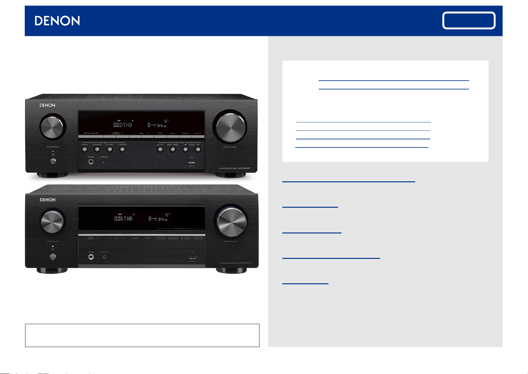
AV SURROUND RECEIVER
AVR-S540BT
AVR-X550BT
Service Manual
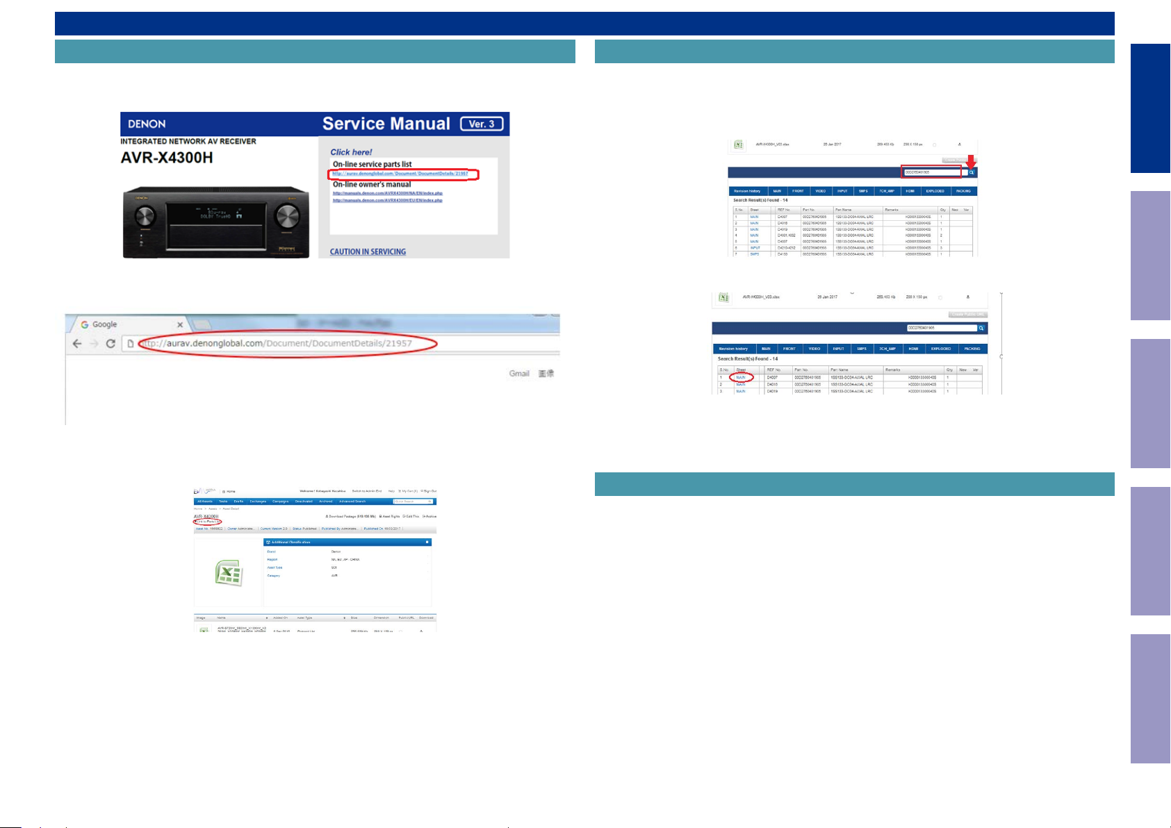
Click here!
On-line service parts list
AVR-S540BT: http://dmedia.dmglobal.com/Document/DocumentDetails/24350
AVC-X550BT: http://dmedia.dmglobal.com/Document/DocumentDetails/24349
ONLINE PARTS LIST (P5)
WEB owner’s manual
NA: http://manuals.denon.com/AVRS540BT/NA/EN/index.php
EU: http://manuals.denon.com/AVRX550BT/EU/EN/index.php
AP: http://manuals.denon.com/AVRX550BT/AP/ZH/index.php
JP: http://manuals.denon.com/AVRX550BT/JP/JA/index.php
Upload is planned for the time of a future press release.
BEFORE SERVICING THIS UNIT
ELECTRICAL
Ver. 1
•Forpurposesofimprovement,specicationsanddesignaresubjecttochangewithoutnotice.
• Please use this service manual whenreferringtotheoperatinginstructionswithoutfail.
• Some illustrations usedinthisservicemanualareslightlydifferentfromtheactualproduct.
MECHANICAL
REPAIR INFORMATION
UPDATING
Page 2
BEFORE SERVICING THIS UNIT
Before Servicing
SAFETY PRECAUTIONS
NOTE FOR SCHEMATIC DIAGRAM
HANDLING THE SEMICONDUCTOR AND OPTICS
ONLINE PARTS LIST
Accessing the Parts List
Searching Part Numbers or Ref. Numbers
NOTE FOR PARTS LIST
SERIAL NUMBER
Serial Number Organization
SKU Code of this Unit
POST-SERVICE PRECAUTIONS
This Unit
Electrical Mechanical Repair Information Updating
Initializing this Unit AVR-S540BT
Initializing this Unit AVR-X550BT
2
Page 3
SAFETY PRECAUTIONS
The following items should be checked for continued protection of the customer and the service technician.
Leakage current check
Before returning the set to the customer, be sure to carry out either (1) a leakage current check or (2) a line to chassis resistance check. If the leakage current exceeds 0.5 milliamps, or if the resistance from chassis to either side of the power cord is less than 460 kohms, the set is defective.
Be sure to test for leakage current with the AC plug in both polarities, in addition, when the set's power is in each state (on, off and standby mode), if applicable.
Before Servicing
This Unit
CAUTION
Please heed the following cautions and instructions during servic-
ing and inspection.
◎ Heed the cautions!
Cautions which are delicate in particular for servicing are labeled on the cabinets, the parts and the
chassis, etc. Be sure to heed these cautions and the cautions described in the handling instructions.
◎ Cautions concerning electric shock!
(1) An AC voltage is impressed on this set, so if you touch internal metal parts when the set is energized,
you may get an electric shock. Avoid getting an electric shock, by using an isolating transformer and
wearing gloves when servicing while the set is energized, or by unplugging the power cord when
replacing parts, for example.
(2) There are high voltage parts inside. Handle with extra care when the set is energized.
◎ Caution concerning disassembly and assembly!
Through great care is taken when parts were manufactured from sheet metal, there may be burrs on the
edges of parts. The burrs could cause injury if ngers are moved across them in some rare cases. Wear
gloves to protect your hands.
◎ Use only designated parts!
The set's parts have specic safety properties (re resistance, voltage resistance, etc.). Be sure to use
parts which have the same properties for replacement. The burrs have the same properties. In particular,
for the important safety parts that are indicated by the z mark on schematic diagrams and parts lists,
be sure to use the designated parts.
◎ Be sure to mount parts and arrange the wires as they were originally placed!
For safety seasons, some parts use tapes, tubes or other insulating materials, and some parts are mounted away from the surface of printed circuit boards. Care should also be taken with the positions of the
wires by arranging them and using clamps to keep them away from heating and high voltage parts, so
be sure to set everything back as it was originally placed.
◎ Make a safety check after servicing!
Check that all screws, parts and wires removed or disconnected when servicing have been put back
in their original positions, check that no serviced parts have deteriorated the area around. Then make
an insulation check on the external metal connectors and between the blades of the power plug. And
otherwise check that safety is ensured.
(Insulation check procedure)
Unplug the power cord from the power outlet, disconnect the antenna, plugs, etc., and on the power.
Using a 500V insulation resistance tester, check that the insulation resistance value between the inplug
and the externally exposed metal parts (antenna terminal, headphones terminal, input terminal, etc.) is
1M Ω or greater. If it is less, the set must be inspected and repaired.
CAUTION
Many of the electric and the structural parts used in the set have special safety properties. In most cases
these properties are difcult to distinguish by sight, and the use of replacement parts with higher ratings (rated power and withstand voltage) does not necessarily guarantee that safety performance will
be preserved. Parts with safety properties are indicated as shown below on the wiring diagrams and the
parts list in this service manual. Be sure to replace them with the parts which have the designated part
number.
(1) Schematic diagrams Indicated by the z mark.
(2) Parts lists Indicated by the z mark.
The use of parts other than the designated parts could cause electric shocks, res or other dangerous
situations.
Concerning important safety parts
Electrical Mechanical Repair Information Updating
3
Page 4
NOTE FOR SCHEMATIC DIAGRAM
WARNING:
Parts indicated by the z mark have critical characteristics. Use ONLY replacement parts recommended
by the manufacturer.
CAUTION:
Before returning the set to the customer, be sure to carry out either (1) a leakage current check or (2)
a line to chassis resistance check. If the leakage current exceeds 0.5 milliamps, or if the resistance from
chassis to either side of the power cord is less than 460 kohms, the set is defective.
WARNING:
DO NOT return the set to the customer unless the problem is identied and remedied.
Before Servicing
This Unit
NOTICE:
(1) ALL RESISTANCE VALUES IN OHM. k=1,000 OHM / M=1,000,000 OHM
(2) ALL CAPACITANCE VALUES ARE EXPRESSED IN MICRO FARAD, UNLESS OTHERWISE INDICATED. P
INDICATES MICRO-MICRO FARAD. N INDICATES NANO FARAD.
(3) EACH VOLTAGE AND CURRENT ARE MEASURED AT NO SIGNAL INPUT CONDITION.
(4) CIRCUIT AND PARTS ARE SUBJECT TO CHANGE WITHOUT PRIOR NOTICE.
HANDLING THE SEMICONDUCTOR AND OPTICS
Electrostatic breakdown of the semi-conductors or optical pickup may occur due to a potential difference caused by electrostatic charge during unpacking or repair work.
1. Ground for Human Body
Be sure to wear a grounding band (1 M ohm) that is properly grounded to remove any static electricity
that may be charged on the body.
2. Ground for Workbench
Be sure to place a conductive sheet or copper plate with proper grounding (1 M ohm) on the workbench or other surface, where the semi-conductors are to be placed. Because the static electricity
charge on clothing will not escape through the body grounding band, be careful to avoid contacting
semi-conductors with your clothing
<Incorrect>
<Correct>
CBA
1MΩ
Grounding Band
CBA
Conductive Sheet or
Copper Plate
1MΩ
Electrical Mechanical Repair Information Updating
4
Page 5
ONLINE PARTS LIST
Accessing the Parts List
(1) Access from the Service Manual
・ Click the URL link on the cover of the service manual.
Examples of display
Searching Part Numbers or Ref. Numbers
You can search a Parts List for part numbers or Ref. numbers.
(1) Enter the part number or Ref. number in the search window of the Parts List, and press the search
button.
(2) The search results are displayed.
The name of the sheet in which the search part is used and the part’s line are displayed.
Before Servicing
This Unit
Electrical Mechanical Repair Information Updating
NOTE : If the web browser does not open automatically, copy the URL and paste it into the address bar
of the web browser and then press Enter.
(2) Accessing the Part List from the Model Asset Screen.
・ Display Model Asset from New SDI.
・ Click the section displayed as ▼ Link to Part Lists under the model name.
NOTE : If the ▼ Link to Parts List section is not displayed, download the parts table from the Asset list.
(3) Next, click the "Sheet" section of the search results.
NOTE FOR PARTS LIST
1. Parts indicated by "
2. When ordering a part, make a clear distinction between "1" and "I" (i) to avoid mis-supplying.
3. A part ordered without specifying its part number can not be supplied.
4. Part indicated by "@" mark is not illustrated in the exploded and packaging view.
WARNING: Parts indicated by the z mark have critical characteristics. Use ONLY replacement parts
recommended by the manufacturer.
nsp
" on this table cannot be supplied.
5
Page 6

SERIAL NUMBER
Serial Number Organization
The 14-digit serial number that contains the code of the manufacturing plant and the manufacturing
date.
14 digits
Before Servicing
This Unit
SKU
code
Factory
code
The last
2digit of year
SKU Code of this Unit
Product SKU SKU Code
AVRS540BTBKE3
AVRX550BTBKE2
AVRX550BTBKE1C
AVRX550BTK
Manufactured
Year, month
Month
(01 ~ 12)
Cumulative
serial number
AZB
AZC
AZD
AZE
Electrical Mechanical Repair Information Updating
6
Page 7
POST-SERVICE PRECAUTIONS
Initializing this Unit
Make sure to initialize this unit after replacing the microcomputer or any peripheral equipment, or the
digital PCB.
AVR-S540BT
Initializing this Unit
Make sure to initialize this unit after replacing the microcomputer or any peripheral equipment, or the
digital PCB.
AVR-X550BT
Before Servicing
This Unit
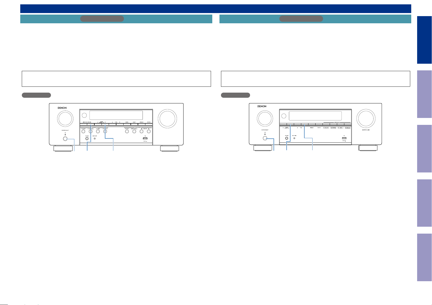
1. Press the power button to turn off the power.
2. While holding down buttons "
the power button to turn on the power.
3. Release the buttons after conrming that the display ashes at 1-second intervals.
* The unit is initialized.
NOTE: • If the unit fails to enter the service mode in step 3, repeat the procedure from step 1.
• Initializing the device restores the customized settings to the factory settings. Write down
your settings in advance and recongure the settings after initialization.
AVR-S540BT
SOUND MODE
SOUND
X
MODE
1
" and "
1
TUNER
PRESET CH +
TUNER PRESET CH+
" simultaneously, press
MASTER VOLUME
1. Press the power button to turn off the power.
2. While holding down buttons "
button to turn on the power.
3. Release the buttons after conrming that the display ashes at 1-second intervals.
* The unit is initialized.
NOTE: • If the unit fails to enter the service mode in step 3, repeat the procedure from step 1.
• Initializing the device restores the customized settings to the factory settings. Write down
your settings in advance and recongure the settings after initialization.
AVR-X550BT
TUNER PRESET CH+
TUNER
X
PRESET CH +
TUNE +
" and "
TUNE +
" simultaneously, press the power
Electrical Mechanical Repair Information Updating
7
Page 8
ELECTRICAL
Before Servicing
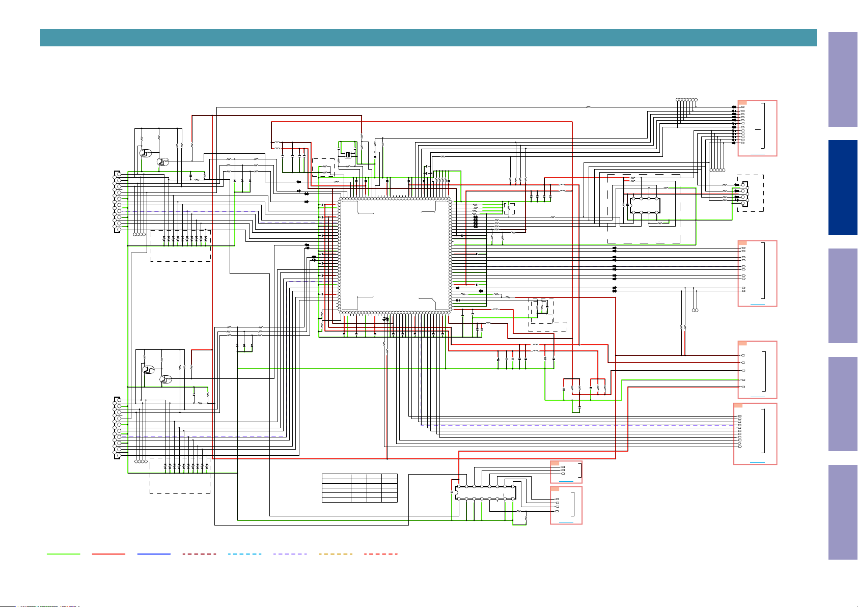
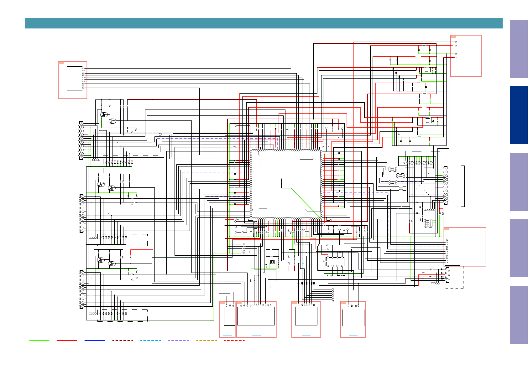
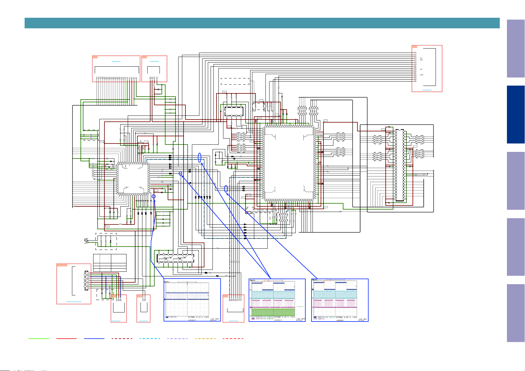
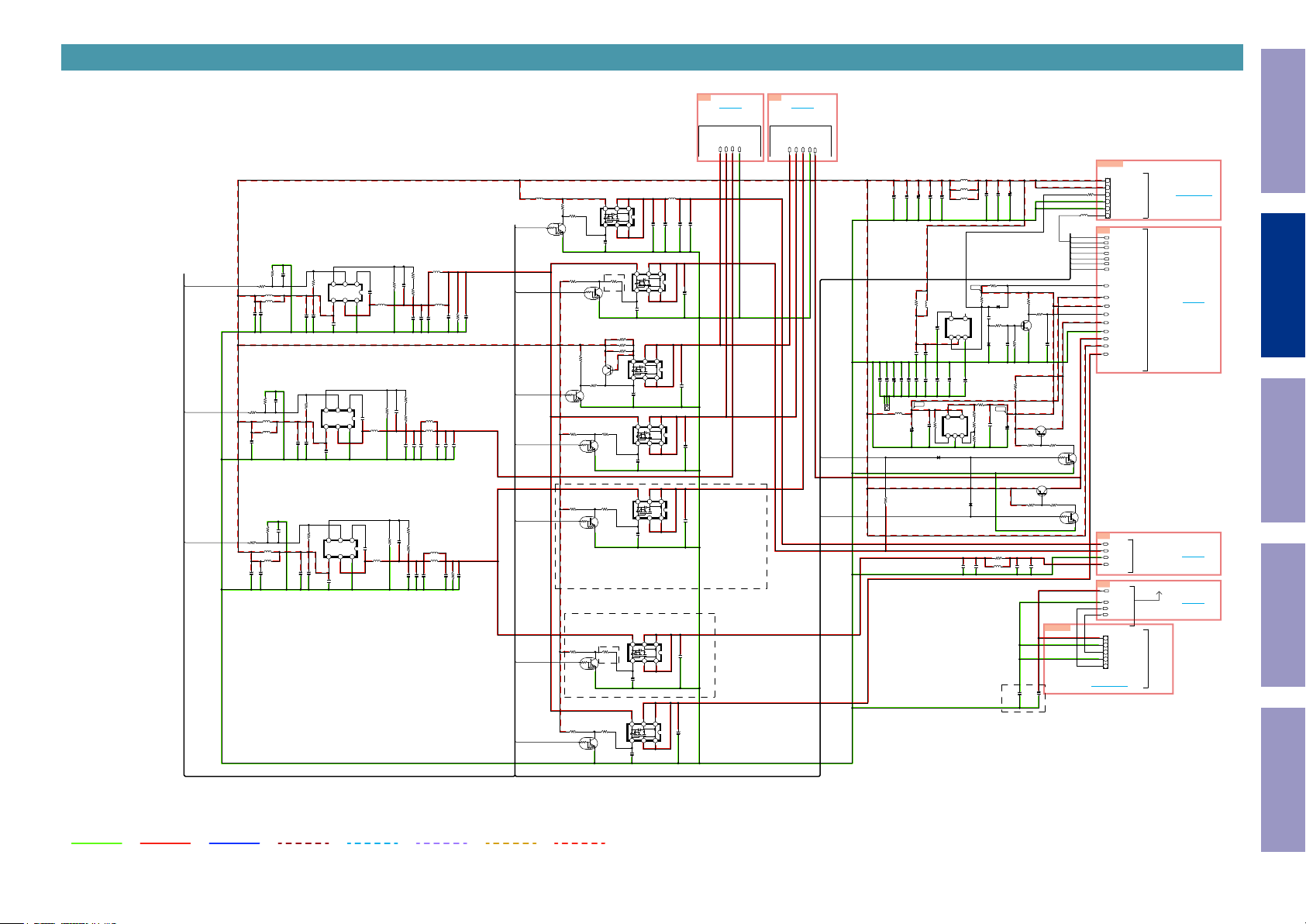
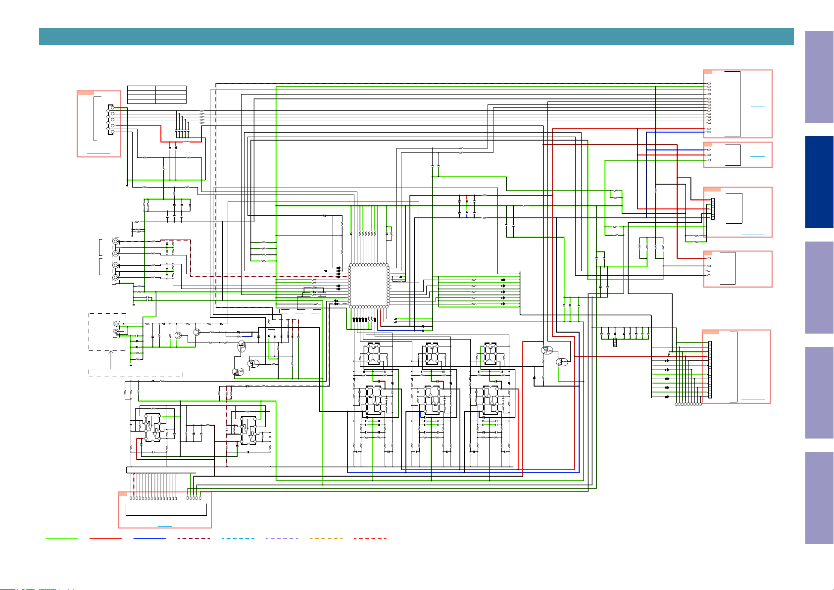
SCHEMATIC DIAGRAMS
SCH01_MCU
SCH02_HDMI OSD
SCH03_HDMI 4K
SCH04_DSP
SCH05_DIGITAL POWER
SCH06_INPUT VOLUME
SCH07_AMP
SCH08_VIDEO, OPTICAL INPUT
SCH09_USB, BT
SCH10_FRONT
SCH11_REGULATOR
SCH12_SMPS
PRINTED CIRCUIT BOARDS
DIGITAL, USB WIRE GUIDE, VIDEO, TUNER, PHONE WIRE GUIDE, FRONT CABLE
GUIDE
MAIN
USB, FRONT, PHONE, STANDBY, MIC
REGULATOR, SMPS
LEVEL DIAGRAM
FRONT ch
CENTER ch
SURROUND ch
SUBWOOFER ch
BLOCK DIAGRAM
ANALOG AUDIO DIAGRAM
DIGITAL AUDIO / HDMI DIAGRAM
VIDEO DIAGRAM
POWER DIAGRAM
WIRING DIAGRAM
SEMICONDUCTORS
1. IC's
2. FL DISPLAY
3. Remote Code Table
This Unit
Electrical Mechanical Repair Information Updating
8
Page 9
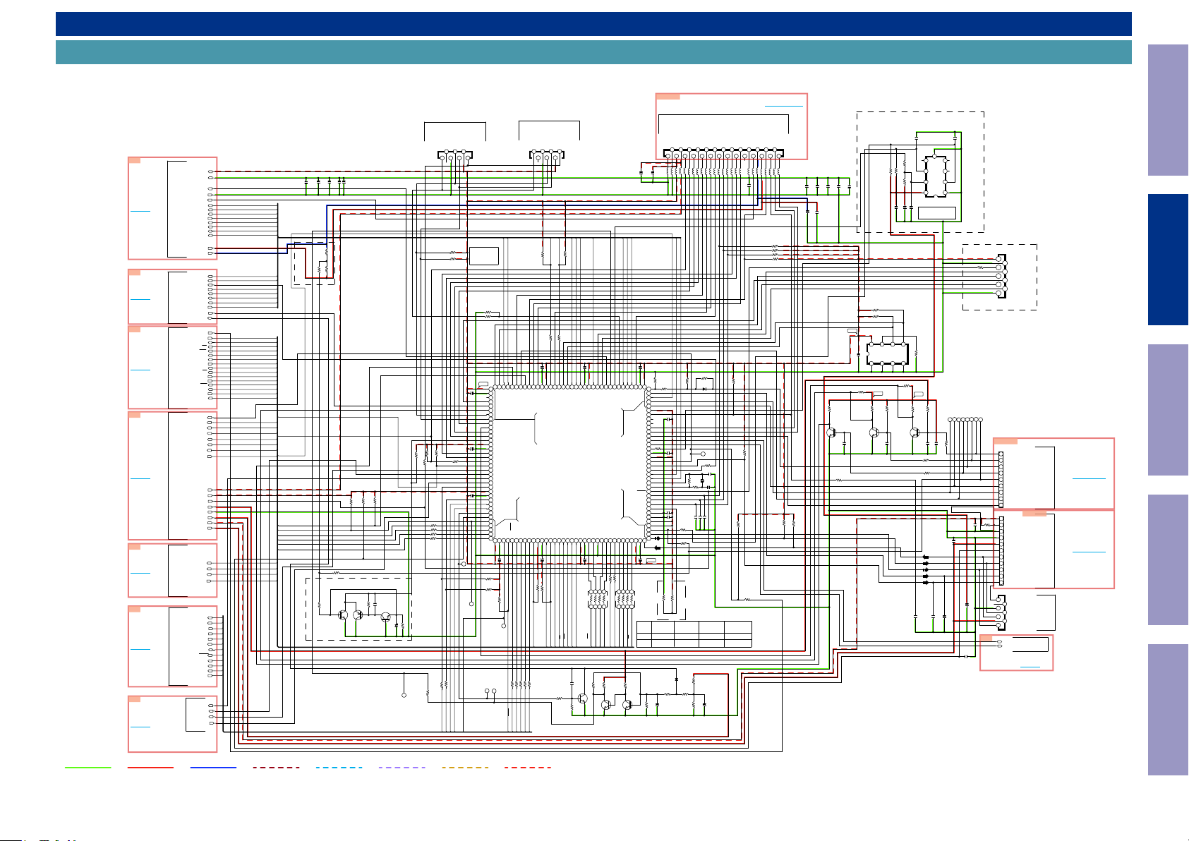
SCHEMATIC DIAGRAMS
TO FRONT B'D
SCH01_MCU
A0
TO 0A
A1
TO 1A
A2
TO 2A
A3
TO 3A
A4
TO 4A
A5
TO 5A
A6
TO 6A
MCU PART
MCU+3V3
AGND
SUB_MUTE
DGND
MIC_SIGNAL
DAC_MUTE
MAIN_VOL_CLK
MAIN_VOL_DATA
TUNER_INT
TUNER_RST
TUNER_CE
TUNER_SDIO
TUNER_SCLK
+12V
TO INPUT/VOLUME PART
-12V
HPD5
HPD4
HPD3
MN864788_HINT
MN864788_SCL
MN864788_SDA
MN864788_RST
MN864788_HAINT1
MN864788_HAINT0
CEC_COM
TO HDMI 4K PART
DIR_INT
CODEC_MUTE
DSP_MODE_SEL
DIR_CE
DIR_RST
DIR_MOSI
DIR_CLK
DIR_MISO
HDMI_SW
DSP_CS
DSP_SPC1_IRQ
DSP_PCP_BSY
DSP_RST
TO DSP PART
DSP_MOSI
DSP_MISO
DSP_CLK
CEC_POWER2
MAIN_POWER
CPU_POWER
CEC_POWER
DV5_POWER
DA_POWER
USB_POWER2
POWER_DOWN
MCU+5V
MCU+3V3
MCU_RST
SWM3V3
FROM/TO DIGITAL POWER PART
DGND
SWM5V
D5V
USB3V3
788_OSD_SPI_CLK
788_OSD_SPI_CS
788_OSD_SPI_MOSI
788_OSD_SPI_MISO
TO HDMI 4K PART
CEC_COM
ADV7623_RST
INT_TX
INT2_RX
_RX
INT
HDMI_SCL
HDMI_SDA
HDMIOSD_HOLD
HDMIOSD_CLK
HDMIO
SD_CS
HDMIOSD_MO
FROM/TO HDMI OSD PART
HDMIOSD_MI
HINSEL_A
HINSEL_B
HINSEL_C
H5V_DET
TO HDMI OSD PART
MAIN_POWER
CPU_POWER
POWER_DOWN
USB_POWER2
DA_POWER
788_OSD_SPI_MOSI
788_OSD_SPI_MISO
788_OSD_SPI_CLK
788_OSD_SPI_CS
Before Servicing
This Unit
FOR UPDATE (MP:OPEN)
FOR UPDATE (AVR-S540BT/X550BT: USE)
7.BOOT
6.N.C
4.RX
3.TX
5.DGND
2.MCU+3V3
1.RESET
7654321
0.1uF
0.1uF
0.1uF
0.1uF
C7143
POWER-FAIL
0.1uF
C7121
C7141
C7120
C7142
47K
R7136
22K
R7147
22K
22K
R7148
R7145
R7130
47K
R7127
R7129
OPEN
OPEN
OPEN
R7124
R7123
R7122
R7131
R7132
R7133
R7134
0
R7196
POWER-FAIL
2.2K
R7166
Q7108
100K
0.1uF
2SC3052
R7167
C7132
Q7110
Q7109
2SC3052
ISA1530AC1
33K
R7168
C7133
100uF/10V
R7170
T7108
BOOT MODE
47K
R7137
HIGH:UPDATE
LOW:NORMAL
0.1uF
C7115
0.1uF
OPEN
OPEN
R7128
R7195
0
1k
C7114
0.1uF
33
33
33
33
T7104
T7103
0
100
0
R7172
R7171
INT_TX
INT_RX
INT2_RX
HDMI_SDA
HDMI_SCL
FOR UPDATE (MP:USE)
FOR UPDATE (AVR-X250BT: ONLY USE)
CN714
FFC 1mm PITCH
MN864788_HINT
MN864788_HAINT1
R7138
10K
R7139
100
MCU+3V3
C7116
R7119
OPEN
R7120
OPEN
T7105
110
109
108107106105104103102101100
DEBUG
DEBUG
VFD_DATA
9998979695949392919089
THERMALDET_B
VFD_CLK
VFD_CE
PWR_FAIL_PROTECT
VDD_9
VSS_9
VOL_DOWN
VOL_UP
CPU_POWER
MAIN_POWER
HINSEL_C
88878685848382818079787776
HINSEL_B
HINSEL_A
H5V_DET
HDMI_SCL
VDD_8
VSS_8
HDMI_SDA
HDMI_INT2
HDMI_INT
CEC_OUT
USB_POWER1
757473
VDD_1
VSS_1
72
71
0.1uF
C7113
OPEN
R7121
T7106
111
MN864788_HINT
HDMI_INT_TX
706968
T7102
ADV7623_RST
113
112
ASO_DET
MN864788_HAINT1
ADV7623_RST
OSD_HOLD
33
LK
HDMIOSD_HOLD
HDMIOSD_C
117
116
115
114
H/P_RLY
VFD_RST
WAKE_UP
USB_POWER2
77.DA_POWER
76.788_OSD_SPI_MOSI
75.788_OSD_SPI_MISO
74.788_OSD_SPI_CLK
73.788_OSD_SPI_CS
OSD_CLK
OSD_CS
OSD_MOSI
OSD_MISO
67
66
6564636261
33
R717733R717633R717433R7173
R7175
HDMIOSD_CS
HDMIOSD_MO
HDMIOSD_MI
118
DV5_POWER
CEC_OUT
CEC_IN
7.BOOT
6.N.C
3.TX
4.RX
5.DGND
3765
4 2
OPEN
R7140
MN864788_SCL
R7143
0.1uF
C7117
122
121
120
119
VSS_10
VDD_10
H/P_DET
GRN_LED
MN864788_SCL
108.VDD
107.VSS_2
106.PCAP_2
105.DEBUG/JTMS
104.MN864788_HAINT0
103.THERMALDET_A
102.UPDATE_RX
101.UPDATE_TX
STM32F101ZG
DV5_POWER
HDMI_SW
VSS_7
CEC_POWER
VDD_7
60
59
0.1uF
C7112
OPEN
OPEN
R7117
R7118
DSP_PCP_BSY
HDMI_SW
CEC_POWER
2.MCU+3V3
1.RESET
1
CN716
FFC 1mm PITCH(ANGLE TYPE)
OPEN
DAC_MUTE
R7142
MN864788_SDA
33
33
R7144
127
126
125
124
123
DAC_MUTE
REMOTE_IN
EEPROM_SDA
EEPROM_SCL
MN864788_SDA
IC711
MCU
DIR_RST
DSP_PCP_BSY
DSP_SPC1_IRQ
DIR_CE
CODEC_MUTE
5857565554
DSP_SPC1_IRQ
DIR_RST
CODEC_MUTE
DIR_CE
C7134
R7178
10K
R7179
FFC WAFER/27P/1.25mm
15.KEY_1
18.RC_IN
20.FL_CE
25.MCU_3V3
27.NC
17.W/G_LED
22.FL_DATA
24.MCU+5V
16.RED_LED
19.FL_RST
21.FL_CLK
23.CPU_POWER
26.DGND
1618
24 22
2026
1517
1925
23 21
27
OPEN
L7101
L7105
L7111
L7110
L7103
L7107
L71020L7104
OPEN
OPEN
C7123
C7122
TUNER_CE
TUNER_INT
131
VDD_11
DSP_RST
1 2 3 4
5 6 7 8
DSP_RST
R7180
KTC2875B
MN864788_RST
132
MN864788_RST
DIR_MOSI
49
DIR_MOSI
133
134
135
DEBUG
DEBUG
1.DC_PROTECT
2.USB_DAC_MUTE
3.POWER_DOWN
4.FRONT_RLY
5.C/S_RLY
33.VDDA
34.CP_SCL
35.USB_RST
36.USB_RX
BOOT1
DIR_CLK
48
47
46
DIR_MISO
DIR_CLK
SWM3V3
4.7K
2.2M
R7181
Q7112
2SC3052
TUNER_RST
0.1uF
C7119
470K
R7101
R7102
144
143
142
141
140
139
138
137
136
BOOT0
CEC_CTL
SW_MUTE
CP_RESET
DIR_MISO
HPD5
DSP_MOSI
HPD4
454443
33
33
R7116
R7115
1 2 3 4
5 6 7 8
DSP_MOSI
HPD5
HPD4
Q7113
TUNER_CE
TUNER_INT
CEC_POWER2
MAIN_VOL_DATA
MAIN_VOL_CLK
DSP_CLK
DSP_MISO
42
41
DSP_CLK
DSP_MISO
47K
R7182
2SC3052
TUNER_RST
MIC_DET
OSC32_IN
OSC32_OUT
ISEL_B
ISEL_A
HI-B_RELY
CVBS_SW2
CVBS_SW5
CP_SDA
USB_EN
XTAL_IN
XTAL_OUT
DSP_CS
40
DSP_CS
0
VDD_3
VSS_3
RED_LED
VBAT
C7101
0.1uF
9 8 7 6 5 4 3 2 1
R7112
OPEN
VSS_5
VDD_5
HPD3
RESET
KEY1
KEY2
KEY3
OPTION
0.1uF
C7105
VSSA
C7106
VREF-
0.1uF
VREF+
USB_TX
VSS_4
VDD_4
36 35 34 33 32 31 30 29 28 27 26 25 24 23 22 21 20 19 18 17 16 15 14 13 12 11 10
39
38
37
MCU+3V3
0.1uF
C7110
R7113
R7114
100x4
OPTION
RN711
*OPTION
S540BTE3
R7113
4K7
R7114
R7184
220K
100K
220P
R7183
C7135
TUNER_SCLK
TUNER_SDIO
0.1uF
C7118
9
128
130
12
VSS_11
TUNER_SDIO
TUNER_SCLK
DSP_MODE_SEL
VDD_6
VSS_6
53
525150
0.1uF
C7111
100x4
RN712
DSP_MODE_SEL
OPEN
100K
Q7111
CEC-PART
L7106
0
FCM601T05
FCM601T05
FCM601T05
MAIN_VOL_CLK
MAIN_VOL_DATA
47K
R7103
0.1uF
C7102
R7107
R7108
R7109
OPEN
R7197
OPEN
OPTION
*OPTION TABLE
X550BTE2
X250BTE2
X
10K
D7102
KDS160RTKP
R7185
27K
L71120L7113
L7108
L7114
L7109
0
0
0
0
0
0
0
R7104
1K
D7101
OPEN
T7101
R7190
33
C7103
20pF
1M
8MHz
X711
C7104
20pF
0
OPEN
OPEN
OPEN
C7109
C7107
C7108
X550BTK
10K
X
SWM5V
1.2K
R7186
3.3K
0.1uF
R7187
C7136
DGND
CN711
TO BN12B1
AVR-X250BT ONLY
FOR AVR-X250BT_BT IOS APP
OPEN
47K
R7164
100
R7165
0.1uF
NC
SCL
RST
8 7 6 5
VCC
IC713
OPEN
2.0c
Apple Auth.
120K
R7162
0.01uF
C7146
C7131
100
C7600
OPEN
C7151
9
4321
NC
NC
SDA
GND
Electrical Mechanical Repair Information Updating
CN715
9PIN WAFER
1
1.MCU+3V3
2
2.DGND
R7152
3
3.RESET
1k
4
4.JTDO
5
5.JTCK
6
6.JTMS
7
7.JTDI
8
8.NJTRST
9
9.DGND
USE ONLY DEBUG
T7116
T7111
T7115
T7110
T7113
T7114
T7117
T7112
S540/X550 ONLY
C7596
0.1uF
C7602
0.1uF
CN712
CN712
987654321
9.THERMALDET_B
8.THERMALDET_A
7.DC_PROT
6.ASO_DET
5.+/-B DETECT
4.C/S_RLY
3.FRONT_RLY
2.H/P_RLY
1.HI-B_RLY
CN713
CN713
1.D5V
R7125
2.D5V/BOOT(SDA)
C7603
0
0.1uF
3.DGND
4.DGND
5.USB3V3
6.USB_POWER1
7.BT_TX
8.BT_RX
9 8 7 6 5 4 3 2 1
9.BX_RST/BT_RST
10.DAC_MUTE
11 10
11.USB_EN/WAKE UP
CN717
7
7.BOOT(SDA)
6
6.N.C
5
5.DGND
4
4.BT_RX
3
3.BT_TX
2
2.BT_3V3
1
1.BT_RESET
A7
CVBS_SW2
CVBS_SW5
TO DSP PART
TO 7A
TO MAIN B'D
WAFER/9P/2.0mm
WAFER/11P/2.0mm
FROM/TO USB/BT B'D
BT UPDATE
X250BT ONLY
TO BN502
TO BN912
100
OPEN
R7163
C7604
OPEN
C7599
0.1uF
0.1uF
C7150
8.MIC_GND
6.-12V
13.KEY_3
14.KEY_2
11.VSEL_A
12.VSEL_B
L7115
L7117
L7116
0
0
0
OPEN
R7105
R7194
X550BTE1C
X250BTE1C
10K
10K10K
1.ISEL_A
3.MIC_DET
10.H/P_DET
7.MIC_SIGNAL
4.POWER_KEY
5.+12V
9.NC
2.ISEL_B
CN711
1011121314
L7119
L7120
0
C7149
FCM601T05
R7106
OPEN
R7193
OPEN
FFC 27P
123456789
L7122
L7123
L7130
L7124
L71260L7127
L7125
0
0
0
0
0
0
0.1uF
0.1uF
0.1uF
C7124
C7126
OPEN
R7149
R7150
R7151
R7188
OPEN
C7125
OPEN
OPEN
C7147
C7148
10K
10K
10K
10K
R7156
OPEN
OPEN
R7110
R7111
CP_SDA
CP_SCL
CP_RESET
OPEN
OPEN
OPEN
R7198
OPEN
R7189
R7192
R7153
R7154
VCC
IC712
A0
1 2 3 4
M24C32WMN6TP
SWM3V3
OPEN
R7158
R7199
OPEN
OPEN
OPEN
C7154
C7153
C7152
2.7K
2.7K
5678
WP
SDA
SCL
R7155
GNDA2A1
R7160
47K
SWM3V3
120K
OPEN
R7159
R7161
Q7107
2SC3052
0.01uF
C7130
C7601
0.1uF
0.1uF
C7127
C7144
MCU+3V3
0.1uF
C7128
R7157
47K
47K
Q7106
Q7105
2SC3052
2SC3052
0.01uF
C7129
R7191
0
GND LINE
POWER+ LINE
POWER- LINE
AUDIO SIGNAL
DIGITAL AUDIO
TMDS SIGNAL
ANALOG VIDEO
STBY POWER
9
Page 10
SCH02_HDMI OSD
HDMI OSD PART
HDMI INPUT-1
(DVD/Blu-ray)
JK721
CJJ9H021Z
19
19.HP DET
18
18.+5V
17
17.GND
16
16.DDC DATA
15
15.DDC CLK
14
14.NC
13
13.CEC
12
12.CK-
11
11.D1 SHIELD
10
10.CK+
9
9.D0-
8
8.D1 SHIELD
7
7.D0+
6
6.D1-
5
5.D2 SHIELD
4
4.D1+
3
3.D2-
2
2.D2 SHIELD
1
1.D2+
T7201
HDMI INPUT-2
(MEDIA PLAYER)
JK722
CJJ9H021Z
19
19.HP DET
18
18.+5V
17
17.GND
16
16.DDC DATA
15
15.DDC CLK
14
14.NC
13
13.CEC
12
12.CK-
11
11.D1 SHIELD
10
10.CK+
9
9.D0-
8
8.D1 SHIELD
7
7.D0+
6
6.D1-
5
5.D2 SHIELD
4
4.D1+
3
3.D2-
2
2.D2 SHIELD
1
1.D2+
T7205
Before Servicing
This Unit
T7224
T7225
T7223
T7220
T7222
T7226
R7231
L7205
L7206
C7229
TO 1B
HINSEL_A
HINSEL_B
HINSEL_C
H5V_DET
TO A6
OPEN
HDMI3_H5V
HDMI4_H5V
HDMI5_H5V
0
HDMI_RESET
INT_TX
INT2
INT1
HDMI_SCL
HDMI_SDA
OPEN
R7223
10K
R7224
8 7 6 5
10K
0.1uF
CLK
VCC
CEC3V3
+1V8H
MI
CLK
MO
CS
TX2+
TX2-
TX1+
TX1-
TX0+
TX0-
TXC+
TXC-
TXDDC_SCL
TXDDC_SDA
0
0
R7238
0
0
R7240
R7239
R7241
OPEN
C7230
0.1uF
C7285
HOLD#
DO
WP#
CS#
R7228
C7281
OSD FLASH PART
ALL VERSION: 32M
FROM HDMI 4K PART
FROM MCU PART
CEC_5V
<PVDD_1V8>
10K
1k
R7255
R7254
Q7201
KRC102S
Q7202
KRC102S
OPEN
T7204
T7202
T7203
D7205
ESD suppressor
ASQS12U020R2
1k
R7267
R7268
Q7204
Q7203
KRC102S
7206
T7207
T7208
T
OPEN
4.7K
47K
47K
R7256
R7257
R7258
0.1uF
R7260
C7270
AA
AA
AA
AA
AA
AA
AA
OPEN
OPEN
OPEN
OPEN
OPEN
OPEN
OPEN
D7208
D7209
D7210
D7211
D7206
D7207
10K
4.7K
47K
47K
R7270
R7269
R7271
KRC102S
C7271
AA
AA
AA
AA
AA
AA
OPEN
OPEN
OPEN
OPEN
OPEN
OPEN
OPEN
D7218
D7219
D7220
D7221
D7222
D7223
D7224
ESD suppressor
ASQS12U020R2
R7261
0
R7263
0
R7265
0
47K
R7259
0
AA
AA
AA
OPEN
OPEN
OPEN
D7212
D7213
D7214
0.1uF
R7273
R7272
0
AA
AA
AA
OPEN
OPEN
OPEN
D7225
D7226
D7227
OPEN
D7201
0
R7274
0
R7276
R7278
0
CEC5V
OPEN
D7216
D7215
47K
AA
L7209
36.7mA
CB03YTYH600
<DVDD_1V8>
+1V8H
L7210
332.4mA
CB03YTYH600
R7262
0
R7264
0
R7266
0
OPEN
OPEN
D7202
D7203
0
R7275
0
R7277
R7279
0
OPEN
OPEN
D7217
0.1uF
C7245
0.1uF
C7242
C7244
10uF/6.3V
500 ohm
R7252
C7246
1K/F
10uF/6.3V
R7253
1K/F
R7296
C7272
0.1uF
C7273
0.1uF
C7274
0.1uF
C7275
0.1uF
C7276
0.1uF
C7277
0.1uF
C7278
0.1uF
OPEN
R7288
10K
R7287
IC723 OPERATION
HDMI FUNCTION
HDMI INPUT1
HDMI INPUT2
HDMI INPUT3
HDMI INPUT4
HDMI INPUT5
10K
R7248
1k
10K
R7247
R7292
OPEN
C7241
15pF
R7249
15pF
X721
C7240
28.636MHz
0
R7250
390K
R7251
0
109
DDCA_SCL
110
CVDD
111
CGND
112
RXA_C-
113
RXA_C+
114
TVDD
115
RXA_0-
116
RXA_0+
117
CGND
118
RXA_1-
119
RXA_1+
120
TVDD
121
RXA_2-
122
RXA_2+
123
HP_CTRLB
124
5V_DETB
125
DGND
126
DVDD
127
DDCB_SDA
128
DDCB_SCL
129
CVDD
130
CGND
131
RXB_C-
132
RXB_C+
133
TVDD
134
RXB_0-
135
RXB_0+
136
CGND
137
RXB_1-
138
RXB_1+
139
TVDD
140
RXB_2-
141
RXB_2+
HP_CTRLC
142
5V_DETC
143
DDCC_SDA
144
1 2 3 4 5 6 7 8 9 10 11 12 13 14 15 16 17 18 19 20 21 22 23 24 25 26 27 28 29 30 31 32 33 34 35 36
C7201
0.1uF
0.1uF
0.1uF
C7239
C7238
XTAL
PVDD
PGND
XTAL1
108.DDCA_SDA
106.5V_DETA
105.HP_CTRLA
107.RTERM
104.PGND
2.CVDD
4.RXC_C-
1.DDCC_SCL
3.CGND
5.RXC_C+
RXC_1-
RXC_0+
RXC_0-
CGND
0.1uF
C7202
0.1uF
C7237
C7236
0.1uF
888990919293949596979899100101102103104105106107108
DVDD
DGND
RESETB
PWRDNB
AP5_OUT
AP1_OUT
AP2_OUT
AP3_OUT
AP4_OUT
AP0_OUT
SCLK_OUT
MCLK_OUT
103.PVDD
IC721
ADV7623BSTZ
6.TVDD
DVDD
DDCD_SDA
TVDD
DGND
RXC_1+
RXC_2-
HP_CTRLD
5V_DETD
DDCD_SCL
CVDD
CGND
RXC_2+
0.1uF
0.1uF
C7203
0.1uF
C7204
C7205
OPEN
R7290
4.7K
R7295
C7232
OPEN
C7233
OPEN
C7235
0.1uF
0.1uF
C7234
INT
INT2
DGND
DVDD
INT_TX
DVDDIO
DGNDDIO
.AP0_IN
75.AP2_IN
77
76.AP1_IN
33.RXD_2+
32.RXD_2-
34.CVDD
35.CGND
RXD_C-
CGND
RXD_0-
TVDD
RXD_0+
RXD_1-
RXD_C+
0.1uF
C7206
CEC5V
S1(10PIN)
S0(11PIN)
S2(9PIN)
L
HH
H
L L
H
H
L
HH
L
HH
H
CVISN74CBT3251P
R7246
100
10K
10K
10K
10K
R7244
R7245
R7242
R7243
737475767778798081828384858687
72
SCL
DGNDIO
71
AP4_IN
SDATA
70
AP5_IN
69
SCLK_IN
68
MCLK_IN
67
EP_MISO
66
EP_MOSI
74.AP3_IN
73.DVDDIO
65
EP_CS
64
EP_SCK
63
CSB
62
ALSB
61
DVDD
60
DGND
59
CEC
58
TXGND
57
TX2+
56
TX2-
55
TXAVDD
54
TX1+
53
TX1-
52
TXGND
51
TX0+
50
TX0-
49
TXGND
48
TXC+
47
TXC-
46
TXGND
45
TXAVDD
44
TXDDC_SCL
43
TXDDC_SDA
42
ARC+
41
36.TXPVDD
HP_ARC-
40
EXT_SWING
39
TXPLGND
TXPGND
38
TXPLVDD
37
TVDD
RXD_1+
<TXPVDD_1V8>
0.1uF
0.1uF
C7207
C7208
IC723
C7282
WR
0.1uF
C7231
10K
R7216
R7215
10K
10K
R7214
R7213
10K
R7212
R7211
R7210
R7209
C7223
0.1uF
R7206
C7222
0.1uF
C7221
0.1uF
R7204
10K
<TXPLVDD_1V8>
CB03YTYH600
1uF
C7218
0.1uF
C7217
L7203
5.2mA
CB03YTYH600
0.1uF
C7280
C7216
10uF/6.3V
<CVDD_1V8>
503.6mA
VCC
0.1uF
B3B4B2
B1
1 2 3 4 5 6 7 8
ANCOE
4.7K
4.7K
4.7K
4.7K
<DVDDIO_3V3>
R7221
R7219
R7218
R7220
<TXAVDD_1V8>
OPEN
R7217
33
33
33
OPEN
R7208
47K
47K
OPEN
R7207
R7205
R7203
OPEN
10K
L7204
24.8mA
D1V8H
<TVDD_3V3>
292.2mA
0.1uF
C7212
0.1uF
C7210
C7211
C7209
10uF/6.3V
100uF/50V
1.5mA
15mA
0.1uF
0.1uF
C7226
C7224
C7225
10uF/6.3V
2K/F
1.6K/F
R7202
R7201
about 888.8ohm
Recommended
: 887 ohm(1%)
place R7201 & R7202 & C7220
as close as possible
to pin40 on the bot of PCB
L7202
CB03YTYH600
L7201
CB03YTYH600
C7214
OPEN
C7213
10uF/6.3V
CB03YTYH600
CB03YTYH600
C7227
10uF/6.3V
R7222
33
OPEN
C7220
C7215
OPEN
B1
10111213141516
9
S1
S2
S0B8B7B6B5
GND
R7297
0
6A
OPEN
R7298
T7221
R7229
OPEN
DI
IC722
VSS
4321
EN25QH32B104HIP2B
R7230
OPEN
T7218
T7219
1.8K
1.8K
R7236
R7237
5A
CEC_COM
ADV7623_RST
INT_TX
INT2_RX
INT_RX
HDMI_SCL
HDMI_SDA
HDMIOSD_HOLD
HDMIOSD_CLK
HDMIOSD_CS
HDMIOSD_MO
HDMIOSD_MI
FROM/TO MCU PART
TO A5
Electrical Mechanical Repair Information Updating
T7217
T7214
T7215
T7216
T7213
CN721
FFC 1mm PITCH
R7232
1
1.SCK
100
2
2.DGND
R7233
3
3.MOSI
100
4
4.VCC
100
R7234
5
5./CS
100
R7235
6
6.MISO
7
7.DGND
FOR OSD UPDATE
A8
OSDTX_2+
OSDTX_2-
OSDTX_1+
OSDTX_1-
OSDTX_0+
OSDTX_0-
OSDTX_C+
OSDTX_C-
OSDTX_SCL
OSDTX_SDA
FROM/TO HDMI 4K PART
TO 8A
A9
CEC5V
CEC3V3
D1V8H
DGND
SWM5V
TO 9A
TX1_CTX1_C+
TX1_0TX1_0+
TX1_1TX1_1+
TX1_2-
TX1_2+
TX1_SCL
TX1_SDA
HPDTX1
TO 0B
FROM DIGITAL POWER PART
FROM/TO HDMI 4K PART
B0
GND LINE
POWER+ LINE
POWER- LINE
AUDIO SIGNAL
DIGITAL AUDIO
TMDS SIGNAL
ANALOG VIDEO
STBY POWER
10
Page 11
SCH03_HDMI 4K
HDMI 4K PART
8A
OSDTX_2+
OSDTX_2-
OSDTX_1+
OSDTX_1-
OSDTX_0+
OSDTX_0-
OSDTX_C+
OSDTX_C-
OSDTX_SDA
OSDTX_SCL
FROM HDMI OSD PART
TO A8
19.HP DET
18.+5V
17.GND
16.DDC DATA
15.DDC CLK
14.NC
13.CEC
12.CK-
11.D1 SHIELD
10.CK+
9.D0-
8.D1 SHIELD
7.D0+
6.D1-
CBL/SAT(4K)
HDMI_INPUT-3
5.D2 SHIELD
4.D1+
3.D2-
2.D2 SHIELD
1.D2+
19.HP DET
18.+5V
17.GND
16.DDC DATA
15.DDC CLK
14.NC
13.CEC
12.CK-
11.D1 SHIELD
10.CK+
9.D0-
8.D1 SHIELD
7.D0+
6.D1-
5.D2 SHIELD
HDMI_INPUT-4
Blu-ray(4K)
4.D1+
3.D2-
2.D2 SHIELD
1.D2+
19.HP DET
18.+5V
17.GND
16.DDC DATA
15.DDC CLK
14.NC
13.CEC
12.CK-
11.D1 SHIELD
10.CK+
9.D0-
8.D1 SHIELD
7.D0+
6.D1-
GAME(4K)
HDMI_INPUT-5
5.D2 SHIELD
4.D1+
3.D2-
2.D2 SHIELD
1.D2+
GND LINE
POWER+ LINE
JK723
CJJ9H021Z
19
18
17
16
15
14
13
12
11
10
9
8
7
6
5
4
3
2
1
JK724
CJJ9H021Z
19
18
17
16
15
14
13
12
11
10
9
8
7
6
5
4
3
2
1
JK725
CJJ9H021Z
19
18
17
16
15
14
13
12
1
1
10
9
8
7
6
5
4
3
2
1
POWER- LINE
Before Servicing
B2
CEC5V
CEC3V3
DGND
CEC1V1
OPEN
OPEN
C7398
C7386
TO 2B
TO DIGITAL POWER PART
JK726
CJJ9H021Z
1
1.D2+
2
2.D2 SHIELD
3
3.D2-
4
4.D1+
5
5.D2 SHIELD
6
6.D1-
7
7.D0+
8
8.D1 SHIELD
9
9.D0-
10
10.CK+
11
11.D1 SHIELD
12
12.CK-
13
13.CEC
14
14.UTIL/HEAC+
15
15.DDC CLK
16
16.DDC DATA
17
17.GND
18
18.+5V
19
19.HP DET
0.1uF
D7333
OPEN
A A
MONITOR
HDMI_OUT
0B
TX1_C-
TX1_C+
TX1_0-
TX1_0+
TX1_1-
TX1_1+
TX1_2-
TX1_2+
TX1_SCL
TX1_SDA
HPDTX1
1
1.SCK
2
2.DGND
3
3.MOSI
4
4.VCC
5
5./CS
6
6.MISO
7
7.DGND
CN731
FFC 1mm PITCH
T7339
TO B0
FROM/TO HDMI OSD PART
FOR OSD UPDATE
C7346
OPEN
3
4
C7356
ESD suppressor
ASQS12U020R2
D7332
D7331
A A
A A
1.8K
R7363
C7355
OPEN
D7330
1.8K
R7364
L7302
CB05YTYH221
CB05YTYH221
4.7uF/6.3V
D7329
A A
R7365
C7339
C7343
4.7uF/6.3V
C7393
L7304
C7358
C7361
L7308
CB05YTYH221
D7328
A A
A A
0
C7340
1uF
R7366
10uF/6.3V
C7394
C7395
C7396
D7327
1uF
51/F
L7301
CB05YTYH221
10uF/6.3V
L7305
4.7uF/6.3V
L7306
CB05YTYH221
4.7uF/6.3V
10uF/6.3V
10uF/6.3V
OPEN
D7326
A A
C7341
R7367
R7382
100
R7384
100
OPEN
L7303
L7309
CB05YTYH221
C7354
CB05YTYH221
D7325
A A
A A
1uF
T7321
51/F
1234
L7307
L7310
D7324
OPEN
RN735
10x4
C7342
C7344
4.7uF/6.3V
CB05YTYH221
C7357
C7360
C7380
D7323
A A
T7323
T7322
R7381
R7383
100
4.7uF/6.3V
10uF/6.3V
OPEN
C7365
C7397
4.7uF/6.3V
4.7uF/6.3V
OPEN
C7367
10uF/6.3V
D7322
D7321
A A
A A
A A
T7325
T7326
T7324
5678
100
T7336
T7337
T7338
VDD33
AVDD33TX
AVDD33RX0
AVDD33RX1
AVDD33RX2
AVDD33RX3
PVDD33
VDD33IO
47K
47K
1k
10K
R7280
R7281
Q7205
KRC102S
AA
T7209
T7210
T7212
T7211
OPEN
OPEN
D7231
D7232
1k
R7302
R7301
Q7301
KRC102S
AA
T7301
T7302
T7303
T7304
D7301AAD7302AAD7303
D7304AAD7305AAD7306
1k
R7312
R7311
Q7303
KRC102S
AA
AA
T7308
T7307
T7305
T7306
D7311
D7312AAD7313AAD7314
R7282
R7283
Q7206
KRC102S
AA
AA
AA
AA
AA
AA
OPEN
OPEN
OPEN
OPEN
OPEN
D7233
D7234
D7235
D7236
D7237
10K
47K
47K
R7304
Q7302
R7303
KRC102S
AA
AA
D7307AAD7308AAD7309
D7310
10K
47K
47K
Q7304
R7313
R7314
KRC102S
AA
AA
AA
AA
D7315
D7317AAD7318
D7316
D7319AAD7320
AUDIO SIGNAL
OPEN
R7284
0.1uF
C7279
R7285
AA
OPEN
D7238
D7239
R7323
C7301
AA
ESD suppressor
ASQS12U020R2
C7302
ESD suppressor
ASQS12U020R2
OPEN
0.1uF
R7306
R7308
OPEN
R7324
0.1uF
OPEN
47K
R7286
0
AA
AA
OPEN
ESD suppressor
ASQS12U020R2
OPEN
D7240
OPEN
47K
R7305
0
R7307
0
0
OPEN
47K
R7315
R7316
0
R7317
R7318
0
0
R7289
R7291
DIGITAL AUDIO
0
0
TMDS SIGNAL
TO HDMI OSD PART
ANALOG VIDEO
R7343
C7390
C7322
C7328
R7341
TX0ARCIN
788_I2C_SCL
788_I2C_SDA
1B
V
HDMI5_H5
HDMI4_H5V
TO B1
STBY POWER
788_HINT
C7388
0.1uF
0.1uF
C7323
C7324
0.1uF
C7325
0.1uF
C7326
0.1uF
C7327
0.1uF
T7330
47
T7309
T7327
T7328
HDMI3_H5V
0.1uF
0.1uF
0.1uF
10K
T7331
788_RST
R7347
R7348
R7349
R7320
R7325
1A
HPD5
10K
0.1uF
R7372
C7321
72
71
70
69
RX0P5V
RX3SDA
RX3SCL
RX2SDA
RX2SCL
VDD11
AVDD33RX1
P1RXCM
P1RXCP
AVDD11RX1
P1RX0M
P1RX0P
AVDD11RX1
P1RX1M
P1RX1P
AVDD11RX1
P1RX2M
P1RX2P
VSS
AVDD33RX0
P0RXCM
P0RXCP
AVDD11RX0
P0RX0M
P0RX0P
AVDD11RX0
99 98 97 96 95 94 93 92 91 90 89 88 87 86 85 84 83 82 81 80 79 78 77 76 75 74 73
P0RX1M
P0RX1P
AVDD11RX0
P0RX2M
P0RX2P
CEC
TX1ARCIN
VDD11
TX0ARCIN
108 107 106 105 104 103 102 101 100
112
111
110
109
47K
0.1uF
OPEN
1000P
C7329
R7342
R7391
C7331
10K
10K
10K
OPEN
10K
OPEN
OPEN
R7322
R7321
HPD3
HPD4
HDMI_SCL
HDMI_SDA
MN864788_SCL
MN864788_HINT
FROM MCU PART
TO A1
68
NIRQ1
72.RX1P5V
104.VSS
105.RX1SDA
106.RX1SCL
107.RX0SDA
108.RX0SCL
NTEST
113
10K
R7371
MN864788_SDA
0.1uF
0.1uF
C7318
C7319
676665
64
63
62
616059
VSS
VDD11
P2RX1P
P2RX2P
P2RX1M
P2RX2M
AVDD11RX2
69.VDD33
71.RX2P5V
70.RX3P5V
VSS
HSDA0
NC/XO
HSCL0
VDD33
SYSCLK/XI
NRESET
120
119
118
117
116
115
114
1k
47
47
0.1uF
0.1uF
C7392
R7344
R7345
R7346
R7350
1M
X731
27MHz
15pF
C7337
0.1uF
0.1uF
0.1uF
0.1uF
C7317
C7320
C7316
C7314
58
57
56
55
545352
51
50
VSS
P2RXCP
P2RX0P
P3RX2P
P2RXCM
P2RX0M
P3RX2M
AVDD11RX2
AVDD11RX2
AVDD33RX2
AVDD11RX3
IC731
MN864788
4.CH1ALRCLK
142.TX1SDA
3.CH1ASD0
143.TX1HPD
2.TX0HPD
144.TX0SCL
1.TX0SDA
VSS
VDD11
LPSA1/SCLK
LPSA0/MOSI
VDD11
MISO
VSS
CH0AMCLK
CH0ABCLK
NCS/CS
VDD33IO
131
130
129
128
127
126
125
124
122
123
121
33
100
100
33
33
0.1uF
100
0.1uF
C7333
R7378
C7334
R7338
R7337
R7356
R7385
R7377
C7330
OPEN
OPEN
R7352
R7354
0
R7351
10K
10K
R7355
R7353
15pF
C7338
0.1uF
4948474645
P3RX1P
P3RX1M
CH0ASD3
CH0ALRCLK
133
132
33
R733533R7334
R7336
C7315
AVDD11RX3
36.NIRQA1
35.VDD11
34.VSS
33.P0TXCM
CH0ASD2
134
0.1uF
0.1uF
0.1uF
C7387
C7313
C7391
44
43424140393837
VSS
VDD33
PVDD33
P3RX0P
P3RXCP
P3RX0M
P3RXCM
AVDD33RX3
AVDD11RX3
AVDD11TX
P0TXCP
P0TX0M
AVDD33TX
P0TX0P
P0TX1M
AVDD11TX
P0TX1P
P0TX2M
AVDD11TX
P0TX2P
VDD11
VSS
P1TXCM
AVDD11TX
P1TXCP
P1TX0M
AVDD33TX
P1TX0P
P1TX1M
AVDD11TX
P1TX1P
P1TX2M
AVDD11TX
P1TX2P
VDD11
VSS
CH1ABCLK
CH0ASD1
CH0ASD0
VDD11
VDD33NCVSS
TX1SCL
143
141
140
139
138
136
135
142
137
33
33
0.1uF
0.1uF
R7333
C7335
C7336
R7387
10
B3
CEC_COM
MN864788_RST
MN864788_HAINT1
MN864788_HAINT0
FROM/TO DSP PART
HDMI_SDATA0
HDMI_SDATA2
HDMI_SDATA1
TO 3B
HDMI_SCLK
HDMI_MCLK
HDMI_LRCLK
HDMI_SDATA3
0.1uF
C7312
R7394
NIRQA0
144
T7333
TX0SCL
T7310
OPEN
363534333231302928272625242322212019181716151413121110
987654321
R7357
OPEN
0.1uF
C7399
R7339
T7332
OPEN
R7358
R7359
R7396
10K
R7397
10K
8 7 6 5
VCC
HOLD#
CS#DOWP#
R7379
33
10K
10K
T7329
R7370
0.1uF
C7389
C7303
0.1uF
0.1uF
C7310
C7311
0.1uF
C7309
0.1uF
0.1uF
C7308
C7304
0.1uF
C7306
0.1uF
C7307
0.1uF
C7305
0.1uF
C7332
0.1uF
TX0SDA
R7360
0
OPEN
T7311
T7312
R7386
10
DI
CLK
VSS
4321
R7398
OPEN
T7319
T7318
T7317
T7316
T7315
T7314
T7313
4A
FROM MCU PART
T7335
IC732
TX1HPD
EN25QH32B104HIP2B
788_OSD_SPI_CLK
TO A4
10K
R7340
788_OSD_SPI_CS
788_OSD_SPI_MOSI
VDD11
1.8K
1.8K
R7393
OPEN
R7369
R7392
788_OSD_SPI_MISO
AVDD11RX0
AVDD11RX1
AVDD11RX2
AVDD11RX3
AVDD11TX
C7351
1234
12
OPEN
OPEN
C7350
C7352
OPEN
C7353
OPEN
C7345
OPEN
OPEN
C7347
C7348
OPEN
C7349
OPEN
OPEN
C7362
OPEN
C7363
D7334
6.8K
MM1Z525V1B
R7368
RN731
0x2
RN732
12
RN733
0x2
3
4
0x2
RN734
EXC24CH900U
R7361
R7362
0
0
This Unit
Electrical Mechanical Repair Information Updating
11
Page 12
SCH04_DSP
FROM/TO MCU PART
CN741
DSP PART
AD_RINAD_RIN+
LIN+
AD_
AD_LIN-
AGND
C7473
0.1uF
C7474
OPEN
*SOUND QUALITY Coutermeasure.
D_SRD_SR+
D_SL+
D_SLD_SWD_SW+
D_CT+
D_CTD_FRD_FR+
D_FL+
D_FL+5VA
CBL/SAT
JK784
COAXIAL
CN741
1.+12V
2.VGND
3.-12V
4.CVBS_SW2
5.CVBS_SW5
6.+5VD
7.OPT1_IN
8.DGND
9.OPT2_IN
FFC WAFER/9P/1.0mm
TO VIDEO/OPTICAL PART
TO CN781
Before Servicing
This Unit
2A
DIR_INT
CODEC_MUTE
B4
TO 4B
FROM/TO INPUT/VOLUME PART
D_CT+
D_SW+
D_SL-
D_SL+
D_SR+
D_CT-
D_FR-
D_FR+
D_FL+
AD_RIN+
AD_RIN-
D_FL-
AD_LIN+
AD_LIN-
*EMI Coutermeasure.
0.1uF
C7477
0.1uF
C7478
0.1uF
C7479
R7480
OPEN
R7481
OPEN
T7401
T7402
T7403
T7404
OPTION
JK784
C7816
R7811
1
2
3
4
5
6
7
8
9
C7801
*EMI PREPARE
+5VD
C7816
S540BTE3
OPEN
C7450
0.1uF
C7451
4.7uF/100V
C7452
0.1uF
C7453
100uF/63V
D_SBRD_SBR+
D_SBL+
D_SBL
-
L7403
OPEN
C7454
+5VD
75
100P
R7811
D7803
O
100pF
O
OPEN
OPEN
C7803
C7802
D_SW-
100
R7478
R7477
100P
C7449
C7448
VQ
17
FILT+
18
REFGND
19
AOUTB4-
20
AOUTB4+
21
AOUTA4+
22
AOUTA4-
23
VA
24
AGND
25
AOUTB3-
26
AOUTB3+
27
AOUTA3+
28
AOUTA3-
29
AOUTB2-
30
AOUTB2+
31
AOUTA2+
32
33 34 35 36 37 38 39 40 41 42 43 44 45 46 47 48
0.1uF
C7455
C7727
0.01uF
470uF/50V
L7404
FCM601T05
OPEN
X550BT ALL
X250BT ALL
OPEN
0.1uF
OPEN
B6
-12V
+12V
VGND_1
TO INPUT/VOLUME PART
TO 6B
D_SR-
DA_GND1
+5VA
AGND
DSP_AUDIO
100
0.1uF
10111213141516
INT
AINR-
RESET
AD0/CS
AD1/CDIN
14.AINR+
15.AINL+
16.AINL-
IC744
CS42528-CQ
DIR + CODEC
34.AOUTB1-
35.AOUTB1+
33.AOUTA2-
AOUTA1+
AOUTA1-
MUTEC
LPFLT
1.37K/F
R7412
1000P
C7456
0.022uF
C7457
0.1uF
C7458
SDA/CDOUT
AGND
100uF/10V
C7459
DGND
VGND
SCL/CCLK
VARX
RXP7/GPO7
0.1uF
C7460
* Cirrus Recommend
VLC
3.CX_LRCK
RXP6/GPO6
0.01uF
C7461
7A
B5
TO 5B
TO DIGITAL POWER PART
+5VD
R7479
OPEN
+5VD
C7445
OPEN
0.1uF
C7446
C7447
100uF/10V
C7728
LRCK1
SCLK1
123456789
64
CX_SDIN2
VD
CX_SDIN3
63
DGND
CX_SDIN4
62
SCLK2
SAI_SCLK
61
LRCK2
SAI_LRCK
2.CX_SCLK
60
1.CX_SDIN1
OMCK
59
ADCIN1
58
ADCIN2
57
SDTO1
CX_SDOUT
56
MCKO
RMCK
55
SDTO2
SAI_SDOUT
54
VLS
53
46.RXP3/GPO3
47.RXP2/GPO2
48.RXP1/GPO1
DGND
52
VD
51
TXP
50
RXP0
49
RXP5/GPO5
RXP4/GPO4
0.01uF
0.01uF
0.1uF
0.1uF
0.1uF
0.01uF
C7464
C7466
C7467
C7465
C7463
C7462
L : A OUT(HDMI off)
H : B OUT( HDMI on)
CVBS_SW2
CVBS_SW5
FROM DSP PART
TO A7
DGND
+1V8H
+3V3D
CB05YTYH221
C7442
100uF/50V
C7443
L7401
0.1uF
OPEN
C7438
OPEN
C7439
C7440
OPEN
C7441
OPEN
0.1uF
C7444
100uF/10V
OPEN
C7472
100
R7476
33
R7475
R7474
R7473
1k
1k
220
R7472
33
R7471
C7471
0.1uF
C7469
0.1uF
+5VD
C7470
C7468
100uF/10V
0
R7482
0
R7483
OPEN
C7475
OPEN
C7476
0.1uF
C7480
8 7 6 5 4 3 2 1
2Y
GND
3Y3B3A4Y4B4AST
9
100
R7449
100uF/10V
*HDMI SPDIF MODE : DIR MASTER
*HDMI I2S MODE : HDMI MASTER
*ADC MODE : DSP MASTER
*DIR MODE : DIR MASTER
1A1B1Y2A2B
SEL
IC745
VCC
16151413121110
SN74AHC157PWR
C7437
0.1uF
R7448
0
(1) SPDIF input
CH1:RXIN0
R7424, R7425: 10K-->3.3K Change.
C7428
24.576MHz
1M
X741
R7403
10pF
C7404
C7403
R7447
100
* Cirrus Recommend
+3V3D
10K
R7426
CS#
0.1uF
8 7 6 5
+3V3D
L7402
10pF
C7405
220uF/10V
68
R7484
68
3B
FROM/TO HDMI 4K PART
R7427
DO
R7429
CB05YTYH221
C7406
68
68
R7431
R7432
HDMI_SDATA1
HDMI_SDATA0
TO B3
100
R7420
SD[0:7]
10K
3.3K
R7428
4321
WP#
DI
CLKNCVCC
10K
R7401
3.3K
RN741
10Kx4
5 6 7 8
RN742
6 7 8
5
10Kx4
R7402
330
1uF
0.01uF
C7407
+3V3D
3.3K
3.3K
R7424
R7425
VSS
IC742
EN25Q80B104HIP
+1V8
C7427
100uF/10V
123456789
PCP/SCP2_IRQ#
1 2 3 4
2 3 4
1
+3V3D
SCP1_CS#
PCP/SCP2_CS#
+3V3D
VDDIO7
C7401
GNDIO7
0.1uF
1011121314151617181920212223242526272829303132333435363738
GPIO3,DDAC
GPIO2,UART_TXD
C7402
VDD7
0.1uF
GPIO1,UART_RXD
GPIO1,UART_CLK,EE_CS#
GND7
XTAL_OUT
XTI
XTO
GNDA
R7404
PLL_REF_RES
5.1K/F
VDDA(3.3V)
C7408
VDD8
0.1uF
DAI1_DATA3,DSD3
DAI1_DATA2,DSD2
GND8
DAI1_DATA1,DSD1
DAI1_DATA0,DSD0
C7409
VDDIO8
0.1uF
DAI1_SCLK,DSD-CLK
DAI1_LRCK,DSD4
GNDIO8
DAI2_LRCK
DAI2_SCLK
DAI2_DATA,DSD5
R7405
3.3K
R7406
3.3K
R7407
10K
R7408
10K
*HDMI AUDIO Countermeasure
0
0
68
R7444
R7443
R7445
R7446
HDMI_SCLK
HDMI_MCLK
HDMI_LRCLK
HDMI_SDATA2
HDMI_SDATA3
100P
C7425
SD5
SD0
SD1
SD2
AD0
AD1
3.3K
3.3K
R7422
R7423
+3V3D
0.1uF
C7424
C7423
124
125
VDD6
SCP1_MISO/SDA
DAO2_D0,HS3
VDD1
OPEN
R7409
0.1uF
122
123
GNDIO6
SCP1_MOSI
1.SCP2_CK
2.SCP2_MISO
3.SCP2_MOSI
4.SCP1_IRQ
35.DAO2_D3
36.DBDA
37.DBCK
38.DAO2_D2
GNDD1
DAO2_SCLK
44
45
0.1uF
OPEN
OPEN
R7410
R7411
117
118
119
120
121
RESET#
VDDIO6
EXT_OE#
EXT_A19
EXT_CS1#
IC741
AUDIO DSP
CS497024CVZ
DAO1_D2,HS2
VDDIO1
DAO2_LRCLK
DAO1_DATA1,HS1
DAO1_D3
49
50
464748
0.1uF
C7412
5 6 7 8
RN743
1 2 3 4
100uF/10V
115
116
GND5
EXT_A18
DAO1_SCLK
DAO1_DATA0,HS0
515253
R7414
33x4
100
R7413
C7426
126
127
128
GNDD6
SCP1_CLK
SCP1/PCP_BSY
TEST
DAO_MCLK
DAO2_D1,HS4
414243
40
39
C7410
AD13
5 6 7 8
5 6 7 8
33x4
RN747
1 2 3 4
C7422
110
111
112
113
114
VDD5
SD_CS#
EXT_A15
EXT_A16
EXT_A17
102.SD_A0,EXT_A0
101.SD_A1,EXT_A1
100.VDDIO5
99.SD_A2,EXT_A2
68.SD_D0,EXT_D0
67.GNDIO2
66.EXT_WE#
65SD_D1,EXT_D1
SD_DQM0
GND2
VDD2
GNDIO1
DAO1_LRCLK
56
57
54
55
0.1uF
C7414
10K
10K
R7415
33
R7416
33x4
RN746
1 2 3 4
0.1uF
107
108
109
SD_RAS#
SD_CAS#
SD_WE#
SD_D5,EXT_D5
SD_D6,EXT_D6
SD_D7,EXT_D7
585960
DA15
DA14
DA13
DA12
+3V3D
103
104
105
106
GNDIO5
100 101 102
SD_A10,EXT_A10
SD_BA0,EXT_A13
SD_BA1,EXT_A14
C7420
GNDD4
0.1uF
SD_A3,EXT_A3
SD_A4,EXT_A4
C7419
VDD4
0.1uF
EXT_CS2#
SD_A5,EXT_A5
GNDIO4
SD_A6,EXT_A6
SD_A7,EXT_A7
C7418
VDDIO4
0.1uF
SD_A8,EXT_A8
SD_A9,EXT_A9
GND3
0.1uF
C7417
SD_A11,EXT_A11
SD_A12,EXT_A12
VDD3
SD_CLKEN
SD_CLKIN
SD_CLKOUT
SD_DQM1
SD_D8,EXT_D8
SD_D9,EXT_D9
GNDIO3
SD_D10,EXT_D10
SD_D11,EXT_D11
C7416
VDDIO3
0.1uF
SD_D12,EXT_D12
SD_D13,EXT_D13
SD_D14,EXT_D14
SD_D15,EXT_D15
65 66 67 68 69 70 71 72 73 74 75 76 77 78 79 80 81 82 83 84 85 86 87 88 89 90 91 92 93 94 95 96 97 98 99
SD_D3,EXT_D3
VDDIO2
SD_D2,EXT_D2
SD_D4,EXT_D4
63
64
61
62
C7415
0.1uF
+3V3D
DA11
DA10 AD12
(3) DAC input
CH1:LRCK
CH2:BCK
CH3:DIN1
AD[0:19]
C7429
M12L16161A5TG2Q
100uF/10V
512K * 16Bit * 2Banks
SD7
SD6 SD4
SD3
SD4
+3V3D
RN748
C7430
0.1uF
1234
5678
DQ1
33x4
C7431
0.1uF
RN749
1234
33x4
SD2
SD1
SD0
SD5
AD12
AD0
AD1
AD13
9 8 7 6 5 4 3 2 1
5678
LDQM
C7432
0.1uF
_WE
25 24 23 22 21 20 19 18 17 16 15 14 13 12 11 10
C7433
0.1uF
AD3
AD2
RN745
AD2
AD
3
DA8
AD4
DA9
AD5
5 6 7 8
1 2 3 4
DA10
33x4
RN744
5 6 7 8
33x4
R7419
33
R7418
33
DA11
AD6
AD7
AD8
DA12
AD9
1 2 3 4
DA13
DA14
DA15
DA0
DA1
DA2
DA3
DA4
DA5
DA6
DA7
DA8
DA9
R7417
33
DA[0:15]
(2) DIR output
CH1:FSDIR1
CH2:64FSDIR1
CH3:DATADIR1
CH4:MCLK
DSP_MODE_SEL
DIR_CE
DIR_RST
DIR_MOSI
DIR_CLK
DIR_MISO
HDMI_SW
DSP_CS
DSP_SPC1_IRQ
DSP_PCP_BSY
DSP_RST
DSP_MOSI
DSP_MISO
DSP_CLK
TO A2
IC743
50
VSS
VDD
49484746454443424140
DQ0
DQ15
RN751
DA7
1234
DQ14
VSSQ
VSSQ
DQ2
DQ13
DQ3
DQ12
VDDQ
VDDQ
DQ4
DQ11
DQ5
DQ10
VSSQ
VSSQ
DQ6
DQ9
39
DQ7
DQ8
38373635343332313029282726
VDDQ
VDDQ
NC
UDQM
_CAS
CLK
CKE
_RAS
NC
_CS
A9
BA
A10/AP
A8
A0
A7
A1
A6
A2
A5
A3
A4
VSS
VDD
5678
DA6
DA5
DA4
33x4
C7436
+3V3D
0.1uF
RN750
DA3
1234
5678
DA2
DA1
DA0
33x4
C7435
0.1uF
SD3
C7434
SD6
15P
SD7
75
R7430
AD9
AD8
AD7
AD6
AD5
AD4
AD[0:19]
Electrical Mechanical Repair Information Updating
GND LINE
POWER+ LINE
POWER- LINE
AUDIO SIGNAL
DIGITAL AUDIO
TMDS SIGNAL
ANALOG VIDEO
STBY POWER
12
Page 13
SCH05_DIGITAL POWER
DV5_POWER
0.1uF
C7526
HDMI 4K
CEC_POWER
DV5_POWER
R7508
33
0.1uF
C7554
HDMI OSD / DSP
R7514
33
0.1uF
C7566
DIGITAL POWER PART
L7506
R7501
33
CB03YTYH600
R7509
L7509
CB03YTYH600
L7510
OPEN
L7514
CB03YTYH600
L7515
100K
R7502
0.1uF
C7518
L7504
L7505
OPEN
C7525
16V/10uF
C7509 16V/10uF
100K
0.1uF
C7553
R7510
16V/10uF
16V/10uF
C7555
C7556
100K
R7515
0.1uF
C7529
R7516
OPEN
C7567
16V/10uF
C7569 16V/10uF
C7568 16V/10uF
VBST
VFB
EN
4 5 6
OPEN
R7503
IC751
0.1uF
C7511
TPS563200DDCR
123
L7484
VIN
SW
(5040) 3.6uH
GND
C7510 16V/10uF
0.1uF
C7512
VBST
VFB
EN
OPEN
4 5 6
IC752
0.1uF
TPS563200DDCR
C7558
123
L7511
VIN
SW
(5040) 2.2uH
GND
0.1uF
C7557
VBST
VFB
EN
OPEN
4 5 6
IC753
0.1uF
TPS563200DDCR
C7571
123
L7516
(5040) 3.6uH
SW
VIN
GND
0.1uF
C7570
CB03YTYH600
33.2K/F
R7506
OPEN
10K/F
R7504
0
R7505
C7513
L7507
OPEN
C7516
C7514
C7515
6.3V/22uF
6.3V/22uF
6.3V/22uF
4.7K/F
R7512
OPEN
10K/F
R7511
L7512
0
OPEN
R7513
C7559
L7513
0
C7561
C7560
C7562
6.3V/22uF
6.3V/22uF
6.3V/22uF
13.7K/F
R7518
OPEN
10K/F
R7517
L7517
0
CB05YTYH221
R7519
C7572
L7518
OPEN
C7574
C7530
C7573
6.3V/22uF
6.3V/22uF
6.3V/22uF
Before Servicing
2B
TO B2
TO HDMI 4K PART
CEC5V
L7508
L7527
CB03YTYH600
10K
R7557
R7558
10K
DA_POWER
Q7521
KRC104S
3 2 1
0.1uF
C7590
D3.3V
R7524
R7525
10K
33K
DA_POWER
47K
R7507
0.1uF
C7517
C7519 OPEN
CEC_POWER
CEC1V1
OPEN
C7564
C7563 0.1uF
C7565 OPEN
CEC_POWER
CEC_POWER
KRC104S
R7527
Q7504
RC104S
K
R7529
10K
KRC104S
R7555
10K
KRC104S
Q7501
*R7525: USB/BT PLAY Coutermeasure.
R7562
R7563
R7564
10K
Q7412
CVTISA1530AC1
R7526
10K
R7530
10K
Q7505
R7556
10K
Q7519
D1.8V
47K
OPEN
C7532
C7531 0.1uF
R7520
*R7554: USB/BT PLAY Coutermeasure.
R7553
R7554
10K
33K
DA_POWER
USB_POWER2
Q7517
KRC104S
* DSP +1V8H OPTION
R7533
R7534
10K
10K
Q7509
KRC104S
654
Q7522
FDC608PZ
C7591
3 2 1
0.1uF
C7549
2.7
2.7
2.7
3 2 1
0.1uF
C7597
3 2 1
0.1uF
C7523
3 2 1
0.1uF
C7588
* HDMI OSD D1V8H OPTION
3 2 1
0.1uF
C7586
654
3 2 1
0.1uF
C7527
CB03YTYH600
OPEN
OPEN
OPEN
0.1uF
C7522
C7521
C7520
654
Q7502
FDC608PZ
0.1uF
C7550
654
Q7503
FDC608PZ
0.1uF
C7598
654
Q7506
FDC608PZ
0.1uF
C7524
654
Q7520
FDC608PZ
0.1uF
C7589
654
Q7518
FDC608PZ
0.1uF
C7587
Q7510
0.1uF
C7528
FDC608PZ
9A
TO A9
TO HDMI OSD PART
DGND
CEC3V3
CEC1V1
SWM5V
CEC5V
CEC3V3
DGND
D1V8H
CN751
CN751
MAIN_POWER
SWM3.3V
KRC102S
YMW025-06R
1.D5.2V
2.D5.2V
L7429
CB03YTYH600
R7450
3.M_RESET
0
4.D_GND
5.D_GND
6 5 4 3 2 1
6.MAIN_POWER
3A
CEC_POWER2
MAIN_POWER
CPU_POWER
CEC_POWER
DV5_POWER
DA_POWER
USB_POWER2
POWER_DOWN
MCU+5V
MCU+3V3
MCU_RST
SWM3V3
DGND
SWM5V
D5V
USB3V3
WAFER/6P/2.5mm
FROM/TO SMPS B'D
FROM/TO MCU PART
TO BN601
TO A3
SWM5V
Q7516
5B
+5VD
+3V3D
DGND
+1V8H
B7
+5VA
DA_GND2
USB/BT_L
USB/BT_R
CN752
CJP05GI288ZY
1
1.+5VA
2
2.DA_GND
3.USB/BT_R
4.DA_GND
5 4 3
5.USB/BT_L
TO BN914
TO B5
TO DSP PART
FROM/TO INPUT/VOLUME PART
TO 7B
TO USB/BT B'D
WAFER/5P/2.0mm
CPU_POWER
CEC_POWER2
L7501
CB03YTYH600
L7502
CB03YTYH600
L7503
0.1uF
0.1uF
C7501
C7502
0.1uF
OPEN
OPEN
C7506
C7508
C7507
C7504
C7505
470uF/16V
OPEN
R7541
L7129
OPEN
C7551
OPEN
OPEN
C7788
C7542
OPEN
0.1uF
0.1uF
0.1uF
0.1uF
0.1/50V
OPEN
1uF
0.01uF
C7785
C7784
C7576
C7577
C7592
C7594
C7575
C7593
MCU+5V
ET751
OPEN
L7521
CB03YTYH600
1k
1/10V
IC756
OPEN
C7578
AP7361-Y-13
C7745
R7746
D7503
OPEN
OPEN
R7780
C7503
OPEN
CB03YTYH600
IC755
OPEN
51
4
NC
VDD
GNDCDOUT
2
3
1uF
C7786
C7787
4
51
IN
OUT
GND
EN
ADJ/NC
3
2
C7582
470uF/16V
R7543
MCU+3V3
10K
10K
R7542
D7501
100K
R7545
KDS160
R7546
Q7512
100
2SC3052
1uF
C7544
R7544
4.7K
0
47K
0.1uF
D7502
KDS16
C7543
0.01uF
R7761
MCU+3V3
0
47K
R7749
0
R7750
C7746
4.7/10V
C7581
15K
R7751
OPEN
D7504
R7552
0
L7522
OPEN
OPEN
C7583
OPEN
0.1uF
C7545
R7547
0
R7779
Q7513
OPEN
OPEN
R7549
R7548
OPEN
OPEN
Q7514
OPEN
Q7515
ISA1530AC1
R7551
R7550
3.3K
10K
OPEN
C7584
C7585
OPEN
CN752
C7595
C7145
0.1uF
0.1uF
*EMI Coutermeasure.
This Unit
Electrical Mechanical Repair Information Updating
GND LINE
POWER+ LINE
POWER- LINE
AUDIO SIGNAL
DIGITAL AUDIO
TMDS SIGNAL
ANALOG VIDEO
STBY POWER
13
Page 14
SCH06_INPUT VOLUME
WIRE/7P/2.0mm
Before Servicing
This Unit
TU771
TU771
CJP09HJ282X
13
1.CH_GND
2
2.INT
3./RST
46
4./CE
57
5.SDIO
6.SCLK
7.VCC
8
8.R-OUT
9
9.L-OUT
FROM TUNER MODULE
TUNER MODULE
TO BN508
JK771
L CH
CBL/
SAT IN
R CH
L CH
MEDIA
R CH
PLAYER IN
JK772
SW2
SW1
PRE OUT
SUBWOOFER
* AVR-S540BT/X550BT: JK 772 (2P RCA JACK:CJJ4N121ZD)
* AVR-X250BT: JK 772 (1P RCA JACK:CJJ4M103ZD)
*TUNER MODULE OPTION
AVR-S540BT E3
AVR-X550BT/X250BT E2
AVR-X550BT/X250BT E1C
AVR-X550BT K
CHGND
R7627
R7654
CHGND
CHGND
C7638
0.1uF
D7603
OPEN
D7604
OPEN
R7764
R7765
CHGND
15K
150K
R7742
R7732
220P
C7704
100
R7745
AD_RIN-
INPUT/VOLUME PART
CNVYST990-A9U2
CNVYST990-D8E3
CNVYST990-A2J1
CNVYST990-A9U2
R7601
270
R7602
270
OPEN
OPEN
R7658
R7659
DGND
0
OPEN
R7740
OPEN
R7615
100
R7616
100
R7619
100
R7620
100
R7655
0
R7738
C7702
0
OPEN
C7703
0.1uF
22uF/50V
R7614
220
330P
R7623
C7639
OPEN
OPEN
C7629
R7741
22uF/50V
OPEN
R7743
R7611
4.7K
4321
CM2
4.7K
R7744
CM1
8 7 6 5
IC766
0.1uF
C7705
NJM2740V
C7706
2700P
R7637
100
100
R7651
100
R7653
100
R7656
100
R7657
100P
100P
100P
0.1uF
100P
C7612
C7613
C7610
C7614
C7611
L7601
CB03YTYH600
C7607
0.1uF
C7605
470uF/16V
R7605
0
27K
R7603
R7606
0
27K
R7604
0.1uF
0.1uF
0.1uF
C7622
C7621
C7739
0.1uF
0.1uF
0.1uF
C7737
C7738
C7736
1M
220P
C7619
R7617
1M
220P
C7620
R7618
1M
220P
R7621
C7623
1M
220P
C7624
R7622
C7642
R7625
R7638
470
Q7610
KTC2875B
100K
100K
R7624
0
4.7K
C7708
R7747
OPEN
R7757
100
R7748
AD_RIN+
C7643
470
22uF/50V
R7641
Q7611
OPEN
OPEN
R7626
R7648
10K
AGND
12K
C7707
1K
15K
OPEN
R7728
R7729
R7758
10K
C7710
0.1uF
C7709
100uF/16V
R7753
AD_LIN-
0A
MCU+3V3
AGND
SUB_MUTE
MIC_SIGNAL
DGND
DAC_MUTE
MAIN_VOL_CLK
MAIN_VOL_DATA
TUNER_INT
TUNER_RST
TUNER_CE
TUNER_SDIO
TUNER_SCLK
+12V
-12V
100
R7639
100
R7640
OPEN
C7634
OPEN
C7633
R7772
R7736
150(1W/6432)
Z7.5V
OPEN
D7601
C7630
C7713
C7720
USB/BT_R
10uF/100V
100K
R7633
OPEN
OPEN
OPEN
OPEN
OPEN
OPEN
C7649
C7648
OPEN
DSP_AUDIO
100uF/50V
100K
R7634
TUNER_L
TUNER_R
DCAP_4
26 25 24 23 22 21 20 19 18 17 16 15 14
27
R4IN
28
L4IN
29
SAT_R
30
SAT_L
31
R6IN
NJU72340AFH3
32
L6IN
33
MEDIA_R
34
MEDIA_L
35
DCAP_5
36
MONOIN
DCAP_6
37
ADC_R
38
ADC_L
39
DAC_FL
DAC_FR
AGND
R7684
C7666
R7682
C7663
50V/47uF
100
R7726
C7661
3K/F-T
R7678
R7679
C7658
1500P
2K
R7676
2.4K/F-T
R7670
C7652
1500P
D_FL-
R7628
R7632
R7631
L2IN
R2IN
IC761
DAC_SL
DAC_C
OPEN
IC762
NJM8080G
330P
2K
0.1uF
C7656
330P
C7654
1500P
R7674
3K/F-T
R7671
2.4K/F-T
D_FL+
R7775
0
R7776
0
R7777
0
R7778
0
* R7608: AVR-X250BT(NOT USED)
MCU+3V3
820
R7652
0.1/50V
C7644
R7647
470K
C7645
Q7612
KRA104S
Q7613
Q7614
KRA104S
KRC104S
C7627
22uF/50V
150K
R7727
R7754
4.7K
4321
CM2
4.7K
220P
R7752
CM1
8 7 6 5
IC767
0.1uF
C7712
100
NJM2740V
C7617
2700P
D7606
Z3.9V
D7605
D7608
KDS160
KDS160
D7609
KDS160
10uF/50V
47K
R7650
R7649
R7669
10K
R7730
0
4.7K
C7711
OPEN
R7755
100
R7756
AD_LIN+
C7721
USB/BT_L
10uF/100V
OPEN
R7635
OPEN
R7636
R7782
100uF/50V
C7646
0
R7608
R7660
OPEN
OPEN
D7607
KDS160
C7632
47K
DGND
OPEN
R7783
100uF/50V
R7642
R7643
R7629
REC_L
DCAP_3
REC_R
13
CLOCK
12
AGND
DATA
MINI_R
MINI_L
11
SBR_IN2
SBL_IN2
AGND
C7650
10
DCAP_2
100uF/50V
9
DCAP_1
8
SW OUT
R7784
7
SBR OUT
OPEN
6
SBL OUT
5
SR OUT
4
SL OUT
3
C OUT
2
FR OUT
FL OUT
1
DAC_SR
DAC_SBR
DAC_SBL
DAC_SW
52515049484746454443424140
AVCC
AVEE
OPEN
OPEN
DCAP_7
DCAP_8
100uF/50V
C7608
100uF/50V
C7609
R7609
R7610
Q7604
OPEN
123
OPEN
R7685
4 5 6
OPEN
OPEN
C7667
100K
R7683
100K
C7665
0.1uF
C7664
50V/47uF
A OUTPUT
8765
V+
100
B OUTPUT
R7725
A
-
+
A-INPUT
330P
C7662
B
-
+
A+INPUT
3K/F-T
R7680
B-INPUT
2K
R7681
4 3 2 1
V-
B+INPUT
C7660
C7659
1500P
C7657
330P
2K
C7655
R7677
1500P
R7675
3K/F-T
2.4K/F-T
R7673
R7672
2.4K/F-T
C7653
1500P
D_FR-
D_FR+
0.1uF
C7647
0.1uF
C7651
OPEN
R7700
4 5 6
OPEN
C7683
100K
R7698
C7680
IC763
50V/47uF
NJM8080G
100
R7719
A OUTPUT
330P
B OUTPUT
C7678
A
-
+
3K/F-T
A-INPUT
R7694
2K
R7695
+
A+INPUT
4 3 2 1
V-
C7676
0.1uF
C7674
1500P
C7672
330P
2K
C7670
R7692
1500P
R7690
3K/F-T
2.4K/F-T
R7687
R7686
2.4K/F-T
C7668
1500P
D_CT-
D_CT+
100uF/63V
Z7.5V
D7602
OPEN
100uF/63V
C7631
C7716
R7737
150(1W/6432)
R7665
220
R7664
220
R7666
220
R7668
220
R7667
220
Q7606
Q7605
OPEN
123
OPEN
R7701
OPEN
C7684
100K
R7699
C7682
0.1uF
50V/47uF
C7681
8765
V+
100
R7718
1000P
C7679
B
-
R7696
B-INPUT
8.2K/F-T
2K
R7697
B+INPUT
C7675
4700P
C7673
1000P
2K
C7671
R7693
4700P
R7691
8.2K/F-T
2.4K/F-T
R7689
R7688
2.4K/F-T
C7669
1500P
D_SW-
D_SW+
OPEN
OPEN
R7716
4 5 6
OPEN
C7699
C7700
R7715
R7714
100K
C7696
IC764
50V/47uF
NJM8080G
100
R7724
A OUTPUT
330P
B OUTPUT
C7694
A
-
+
3K/F-T
A-INPUT
R7710
2K
R7711
B
+
A+INPUT
B-INPUT
4 3 2 1
V-
B+INPUT
C7693
0.1uF
C7691
1500P
C7689
330P
2K
C7687
R7708
1500P
R7706
3K/F-T
2.4K/F-T
R7703
R7702
2.4K/F-T
C7685
1500P
-
D_SL
D_SL+
R7722
OPEN
OPEN
OPEN
C7789
C7790
MUTE_+B
AGND
SR
AGND
SL
AGND
C
AGND
FR
AGND
FL
AGND
123
OPEN
R7717
OPEN
100K
C7698
0.1uF
C7697
50V/47uF
8765
V+
100
R7723
330P
C7695
-
3K/F-T
R7712
2K
R7713
C7692
1500P
C7690
330P
2K
C7688
R7709
1500P
R7707
3K/F-T
2.4K/F-T
R7705
R7704
2.4K/F-T
C7686
1500P
D_SR-
D_SR+
R7735
OPEN
C7717
R7734
0.1uF
0.1uF
0.1uF
C7618
C7615
C7793
Q7608
OPEN
Q7609
OPEN
OPEN
OPEN
OPEN
R7773
OPEN
R7762
0
R7763
0
0.1uF
0.1uF
C7735
C7734
OPEN
OPEN
C7791
C7792
1uF
OPEN
0.1uF
0.01uF
C7640
C7641
C7741
C7740
ET761
OPEN
C7732
DA_GND1
RLY_GND
OPEN
R7721
OPEN
OPEN
OPEN
R7766
OPEN
R7759
R7767
R7760
1uF
0.1uF
0.1uF
0.01uF
C7743
C7742
C7733
MUTE_+B
OPEN
C7714
FR
AGND
SR
AGND
C
AGND
SL
AGND
FL
6B
-12V
+12V
VGND_1
CN771
CN771
54321
5.DA+5V
4.VGND(RET_GND)
3.+12V
2.RLY_GND
1.-12V
R7774
0
R7781
0
7B
+5VA
DA_GND2
USB/BT_L
USB/BT_R
CN772
CN772
13121110
13.DGND
12.MUTE_+B
11.RLY_GND
10.+12V
987654321
9.FR
8.AGND
7.SR
6.AGND
5.CEN
4.AGND
3.SL
2.AGND
1.FL
T7606
T7609
T7607
T7602
T7608
T7605
T7604
T7603
T7601
TO A0
FROM MCU PART
TO B6
TO DSP PART
TO REGULATOR B'D
TO BN301
TO B7
FROM/TO DIGITAL POWER PART
TO MAIN B'D
WAFER/13P/2.0mm
TO BN501
Electrical Mechanical Repair Information Updating
GND LINE
POWER+ LINE
4B
D_FL-
D_FR-
D_FL+
D_FR+
AD_LIN-
AD_RIN-
AD_LIN+
AD_RIN+
FROM/TO DSP PART
POWER- LINE
D_CT-
D_CT+
TO B4
D_SL-
D_SW-
D_SL+
D_SW+
+5VA
AGND
D_SR-
D_SR+
DA_GND1
AUDIO SIGNAL
VGND
DGND
DIGITAL AUDIO
TMDS SIGNAL
ANALOG VIDEO
STBY POWER
14
Page 15
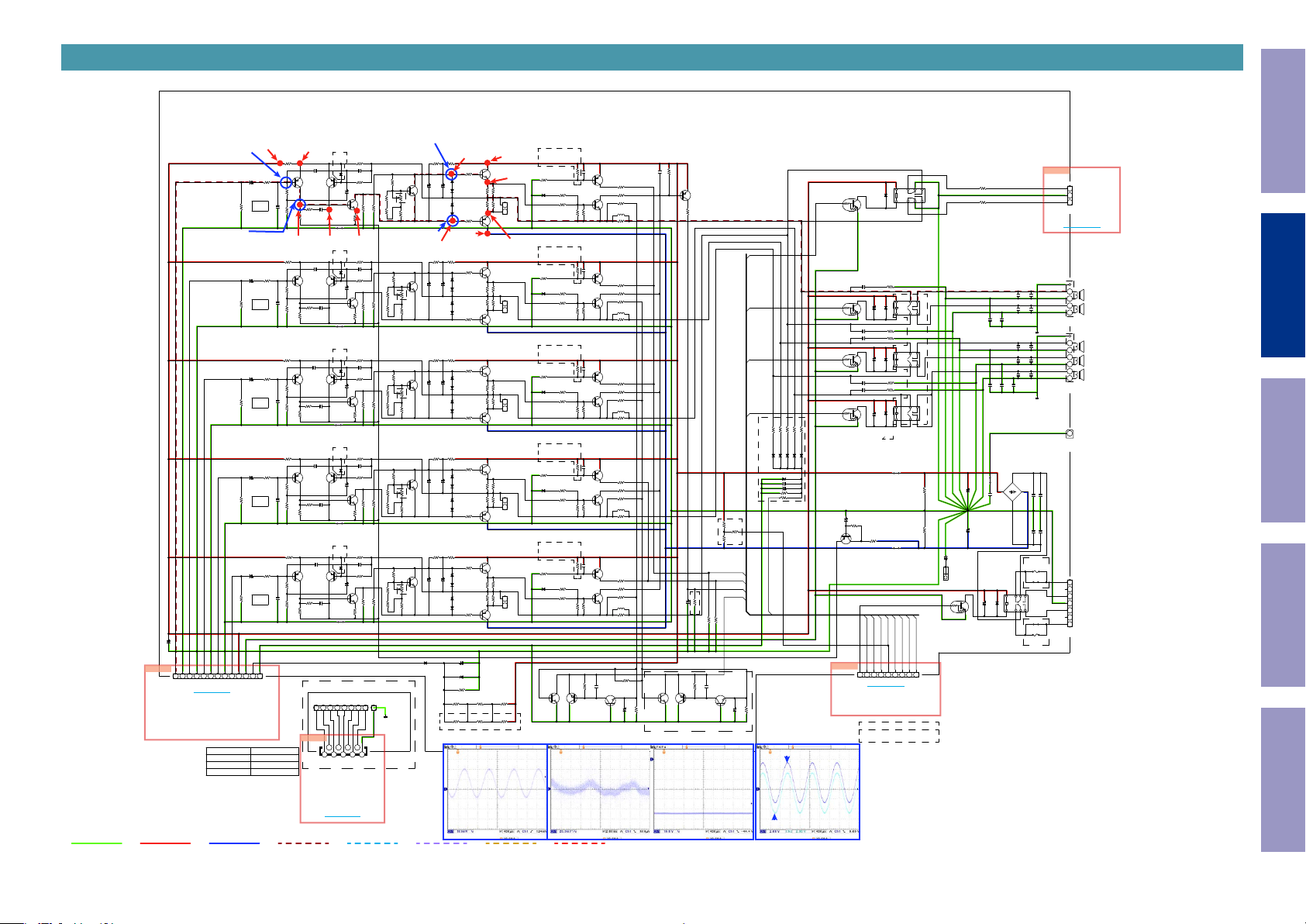
SCH07_AMP
Before Servicing
This Unit
GND LINE
FL_IN
C5723
10UF/50V
BN501
1.FL
POWER+ LINE
M AIN PART
Point A
LEFT FRONT -CH
C5101
50V/47uF
100K
R5101
Point B
LEFT SURROU ND-C H
SL_IN
TO CN772
2.AG ND
4.AG ND
3.SL
TO DIGI TAL B 'D
INP UT/V OLU ME PA RT
2.0 mm 13PIN W IRE
C5201
50V/47uF
100K
R5201
CENT ER-CH
C5301
CEN_ IN
50V/47uF
CEN
100K
R5301
RIGHT SURRO UND -CH
C5401
SR_IN
50V/47uF
100K
R5401
RIGHT FRO NT-C H
C5501
50V/47uF
FR_IN
100K
R5501
987654321
6.AG ND
8.AG ND
7.SR
9.FR
10.+12V
11.RLY _GN D
5.CE N
*TUNER MODULE OPTION
CNVYST990-A9U2
AVR-S540BT E3
CNVYST990-D8E3
AVR-X550BT E2
AVR-X550BT E1C
CNVYST990-A2J1
AVR-X550BT K
CNVYST990-A9U2
POWER- LINE
12V
FL
0.6V
R5103
C5103 82P
10K
Q5101
R5102
KSA992FT A
680
Q5102
KSA992FT A
18K
R5104
R5107
220
C5102 100V/470pF
R5106
R5105 1.2K
1.2K( 1W)
-50.3V -51.0V -50.8V
R5203
C5203 82P
10K
Q5201
R5202
KSA992FT A
680
Q5202
KSA992FT A
18K
R5204
SL
SR
FR
R5207
C5202 100V/470pF
220
R5205 1.2K
R5206
1.2K( 1W)
R5303
C5303 82P
10K
Q5301
R5302
KSA992FT A
680
Q5302
KSA992FT A
18K
R5304
R5307
C5302 100V/470pF
220
R5305 1.2K
R5306
1.2K( 1W)
R5403
C5403 82P
10K
Q5401
R5402
KSA992FT A
680
Q5402
KSA992FT A
18K
R5404
R5407
C5402 100V/470pF
220
R5405 1.2K
R5406
1.2K( 1W)
R5503
C5503 82P
10K
Q5501
R5502
KSA992FT A
680
Q5502
KSA992FT A
18K
R5504
100V/470pF
R5507
C5502
220
R5505 1.2K
R5506
1.2K( 1W)
DGN D
MUT E_+ B
BN501
13121110
12.MU TE_+ B
TUNER MODULE
13.DGN D
BN508
AUDIO SIGNAL
D5101
OPEN
C5104
2200P(M)
J5101
OPEN
D5201
OPEN
C5204
2200P(M)
J5201
OPEN
D5301
OPEN
C5304
2200P(M)
J5301
OPEN
D5401
OPEN
C5404
2200P(M)
J5401
OPEN
D5501
OPEN
C5504
2200P(M)
J5501
OPEN
TU500 YST 990-A9U 2
987654321
BN508
CJP09GI281Z
8.R-O UT
9.L-O UT
7.VC C
TO DIGI TAL B 'D
9P IN B'D TO B'D
TO TU771
Point C1
R5115
R5116
1.10V
5.6K( 1W)
R5108 470K
C5106 33P
R5109 33K
Q5103
R5113
KSC1845FT A
C5105
50V/220uF
515/F
R5133
18
R5134
R5111 OPEN
R5112 OPENR5212 OPENR5312 OPENR5412 OPENR5512 OPEN
R5110
47(1W)
PRE_- B
R5208 470K
C5206 33P
R5209 33K
R5213
Q5203
KSC1845FT A
C5205
50V/220uF
C5305
50V/220uF
C5405
50V/220uF
C5505
50V/220uF
6.SC LK
5.SD IO
515/F
R5233
18
R5234
R5211 OPEN
R5210
47(1W)
R5308 470K
C5306 33P
R5309 33K
R5313
Q5303
KSC1845FT A
515/F
R5333
18
R5334
R5311 OPEN
R5310
47(1W)
R5408 470K
C5406 33P
R5409 33K
R5413
Q5403
KSC1845FT A
515/F
R5433
18
R5434
R5411 OPEN
R5410
47(1W)
PRE_- B PRE_- BPRE_- B
R5508 470K
C5506 33P
R5509 33K
R5513
5503
Q
KSC1845FT A
515/F
R5533
18
R5534
R5511 OPEN
R5510
47(1W)
+12V
DGN D DGN D
AGND AGND
PRE_- B
MUT E_+ B
87654321
CHASSI S
4./C E
3./RS T
2.INT
1.CH_GND
DIGITAL AUDIO
Q5104
KTC3114A
2.7K/ F
VR510
OPEN
560/F
R5114
Point C2
-1.04V
Q5204
KTC3114A
2.7K/ F
VR520
OPEN
560/F
R5214
Q5304
KTC3114A
2.7K/ F
VR530
OPEN
560/F
R5314
Q5404
KTC3114A
2.7K/ F
VR540
OPEN
560/F
R5414
Q5504
KTC3114A
2.7K/ F
VR550
OPEN
560/F
R5514
D5704
1SS133MT
TMDS SIGNAL
C5107
C5207
C5307
C5407
C5507
R5215
5.6K( 1W)
5.6K( 1W)
R5415
5.6K( 1W)
R5515
5.6K( 1W)
5.6K( 1W)
R5117
4.7(1 W)
D5102
OPEN
D5103
C5108
100/63V
50V/47uF
OPEN
0.47(2W )
0.47(2W )
R5119
R5121
D5104
OPEN
R5120
R5122
0.47(2W )
0.47(2W )
D5105
R5118
OPEN
4.7(1 W)
-53.4V
R5216
5.6K( 1W)
R5217
4.7(1 W)
D5202
OPEN
D5203
C5208
100/63V
50V/47uF
OPEN
R5221
R5219
0.47(2W )
0.47(2W )
D5204
OPEN
R5220
R5222
0.47(2W )
0.47(2W )
D5205
OPEN
R5218
4.7(1 W)
R5315
R5316
5.6K( 1W)
R5317
4.7(1 W)
D5302
OPEN
D5303
C5308
100/63V
50V/47uF
OPEN
R5319
R5321
0.47(2W )
0.47(2W )
D5304
OPEN
R5320
R5322
D5305
0.47(2W )
0.47(2W )
OPEN
R5318
4.7(1 W)
R5416
5.6K( 1W)
R5417
4.7(1 W)
D5402
OPEN
D5403
C5408
100/63V
50V/47uF
OPEN
R5419
R5421
0.47(2W )
0.47(2W )
D5404
OPEN
R5420
R5422
D5405
0.47(2W )
0.47(2W )
OPEN
R5418
4.7(1 W)
R5516
5.6K( 1W)
R5517
4.7(1 W)
D5502
OPEN
D5503
C5508
100/63V
50V/47uF
OPEN
R5521
R5519
0.47(2W )
0.47(2W )
D5504
OPEN
R5522
R5520
0.47(2W )
0.47(2W )
D5505
R5518
OPEN
4.7(1 W)
C5717
10UF/50V
D5703
Z6.8V
R5714
OPEN
R5715
R5716
2.2K( 1W)
2.2K( 1W)
R5718
R5719
OPEN
OPEN
OPT.
Point A Point B
ANALOG VIDEO
Q5105
2SD2390
CN510
CJP02GA 01ZY
Q5106
2SB1560
Q5205
2SD2390
CN520
CJP02GA 01ZY
Q5206
2SB1560
Q5305
2SD2390
CN530
CJP02GA 01ZY
Q5306
2SB1560
Q5405
2SD2390
CN540
CJP02GA 01Z
Q5406
2SB1560
Q5505
2SD2390
CN550
CJP02GA 01ZY
Q5506
2SB1560
R5717
2.2K( 1W)
R5720
OPEN
53.4V
PTC T herm ist ors
R5126
PRF18BE 471QB5 RB/85'C
R5123
13mV
470K
D5106
R5124
150K
1SS133MT
21
R5125 10K
R5127
5.6K
9mV
PTC T herm ist ors
R5226
PRF18BE 471QB5 RB/85'C
R5223
470K
D5206
R5224
150K
1SS133MT
21
R5225 10K
R5227
5.6K
PTC T herm ist ors
R5326
PRF18BE 471QB5 RB/85'C
R5323
470K
D5306
R5324
150K
1SS133MT
21
R5325 10K
R5327
5.6K
PTC T herm ist ors
R5426
PRF18BE 471QB5 RB/85'C
R5423
470K
D5406
R5424
Y
150K
1SS133MT
21
R5425 10K
R5427
5.6K
PTC T herm ist ors
R5526
PRF18BE 471QB5 RB/85'C
R5523
470K
D5506
R5524
150K
1SS133MT
21
R5525 10K
R5527
5.6K
AGND
-B
AGNDAGND
PRE_- B
+B +B
DC_F RONT
Q5703
2SC3052
DC PR OTE CTIO N
STBY POWER
Q5704
ISA1530AC 1
MMBTA4 2
MMBTA4 2
MMBTA4 2
MMBTA4 2
MMBTA4 2
R5705
Q5107
0.1uF
C5109
MMBTA9 2
R5129 15K
R5130 22K
Q5108
R5131 22K
L5101
R5128
OPEN
R5132 10( 1W)
Q5207
0.1uF
C5209
MMBTA9 2
R5229 15K
R5230 22K
Q5208
R5231 22K
L5201
R5228
OPEN
R5232 10( 1W)
Q5307
0.1uF
C5309
MMBTA9 2
R5329 15K
R5330 22K
Q5308
R5331 22K
L5301
R5328
OPEN
R5332 10( 1W)
Q5407
0.1uF
C5409
MMBTA9 2
R5429 15K
R5430 22K
Q5408
R5431 22K
L5401
R5428
OPEN
R5432 10( 1W)
Q5507
0.1uF
C5509
MMBTA9 2
R5529 15K
R5530 22K
Q5508
R5531 22K
L5501
R5528
OPEN
R5532 10( 1W)
Q5705
100K
0.1uF
C5710
2SC3052
0.5UH
0
.5UH
0.5UH
DC_F RONT DC_F RONT DC_F RONT
0.5UH
DC_F RONT
0.5UH
R5728
0
C5711
R5706
6.3V/ 470uF
C5701
0.01uF
R5701 10K
FL_OU T
AGNDAGNDAGND
THEMAL DET _A
THEMAL DET _ATHEMAL DET _A
ASOASOASO ASO
+B +B+B+B
DC_S URROU ND
AGND
DC_S URROU ND DC_S URROU ND
-B -B -B -B
THEMAL DET _A
THEMAL DET _B
FR_OU T
-B
+12V+12V+12V
RLY_ GNDRLY_ GNDRLY_ GNDRLY_ GND
DGN D
AGND
PRE_- B
DC_S URROU ND
Q5706
OPEN
10K
DC P ROTE CT O PTIO N ( CE N, SR , SL C H )
Q5701
MMBTA9 2
22K
R5702
CEN_ OUT
FR_OU T
SL_O UT
SL_O UT
CEN_ OUT
FR_OU T
ASO_ DET
FR_OU T
ASO_ DET ASO_ DET ASO_ DET
FR_OU T
2.2K
C5716 47/16V
R5711
R5712 2.2 K
OPEN
C5712
R5707
Q5707
OPEN
SR_O UT
SR_O UT
SR_O UT
R5817
R5818
POWE R DE T.
B+/B -
THER MALDE T_A
THER MALDE T_B
R5713 2.2 K
OPEN
Q5708
OPEN
33K
R5819
33K
ASO_ DET
DC_P ROT
RY560
+12V
FL_OU T
CEN_ OUT
FR_OU T
SL_O UT
SR_O UT
H/P_ RLY
MCU_ CTL
FRONT _RLY
C/S_ RLY
C/S_ RLY
LEVE L DE T.
+B
AGND
DGND
33K
-B
B_DE TEC T
OPEN
OPEN
C5713
R5708
R5814 OPEN
R5815 OPEN
D5810 OP EN
D5811 OP EN
D5807 O PEN
C5806 OPEN
C5807 OPEN
R5810 O PEN
R5811 O PEN
Point C1
R5813 OPEN
D5809 OP EN
R5816 OPEN
D5808 OP EN
D5812 OP EN
+12V
RLY_ GND
B_D ETEC T
PRE_- B
Point C
RLY_ GND
FL_OU T
FR_OU T
SL_O UT
SR_O UT
CEN_ OUT
R5812 OPEN
C5708
100/100V
Q5702
KSA992FT A
HFD27/ 012-H
R5703
33(1W)
C5601
C5602
C5603
D5601
1SS133MT
R5721 10( 2W)
OPEN
D5602
1SS133MT
R5722 10( 2W)
R5723 10( 2W)
OPEN
D5603
1SS133MT
R5724 10( 2W)
R5725 10( 2W)
OPEN
D5604
1SS133MT
615 4
615 4
615 4
J5602
J5604
27183 4
RY562
2 3
RY563
2 3
2 3
RY564
Q5601
KRC105S
C5718 0.047u F
Q5602
KRC105S
C5719 0.047u F
C5720 0.047u F
Q5603
KRC105S
C5721 0.047u F
C5722 0.047u F
Q5604
KRC105S
981-21-12DS
RY562
981-21-12DS
RY563
981-21-12DS
RY564
R5704
100(1W)
PRE_- B
HI-B _RLY
C/S_ RLY
H/P_ RLY
ASO_ DET
DC_P ROT
B_DE TEC T
FRONT _RLY
THER MALDE T_A
BN502
TO CN712
6.ASO _DE T
7.DC _PRO T
5.B_D ETE CT
3.FRO NT_R LY
4.C/S _RLY
2.H/ P_RL Y
1.HI- B_RL Y
TO DIGI TAL B 'D
MC U PAR T
2.0 mm 9PIN WIRE
PTC T herm ist ors
FL-CH , SL- CH, C EN_C H
THER MALDE T_A
FR-CH , SR-C H
THER MALDE T_B
Measurement condition
・Voltage measurement
R5726
470(2W)
6 5
OPEN
R5709
OPEN
R5710
AGND
RLY_ GND
THER MALDE T_B
BN502
987654321
9.TH ERMALD ET_ B
8.TH ERMALD ET_ A
R5727
470(2W)
FL_OU T
FR_OU T
2200P
C5608
C5607
SL_O UT
SR_O UT
CEN_
OUT
2200P
C5612
C5613
OPEN
J5601
C5704
6800uF/63V
OPEN
C5615
D5701
D25SB6 0
C5706
6800uF/63V
0.1/50V
C5707
ET501
CHASSI S
Q5806
OPEN
C5801
KRC105S
D5806
HF115F/012
H/P_ FR
H/P_ FL
C5605
0.018uF
C5606
0.018uF
C5609
0.018uF
C5610
0.018uF
C5611
0.018uF
1
1SS133MT
RY586
2200P
2200P
C5614
2
3
4 351
BN505
1.HP _RCH
2.AGND
3 2 1
3.HP _LCH
BN505
TO FRON T B'D
TO CN104
2.0 mm 3PIN WIRE
Electrical Mechanical Repair Information Updating
C5616
OPEN
C5617
OPEN
C5618
OPEN
C5619
OPEN
C5620
OPEN
2200P
4
726 8
JUMPE R
JUMPE R
1
FL-CH
2
3
FR-CH
4
JK503
CJJ5P047Z D
1
SL-CH
SL-CH
2
3
SR-CH
SR-CH
4
5
C-CH
C-CH
6
JK504
CJJ5R023ZD
BK501
M3 BR ACK ET
CMD1 A569-V1
OPEN
C5714
C5702 250V/0 .1uFC5703 250V/0 .1uF
OPEN
C5715
F5801
OPEN
J5804
1234567
AC_L
N.C
AC_H
CEN
AC_H
N.C
J5805
AC_L
CN503
CJP07GA 90ZY
FRO M MAIN T RAN S
3.96mm 7 PIN W AFE R
F5802
OPEN
No signal
・Waveform measurement
INPUT: 200mVrms / 1KHz (ANALOG)
Point C2
Surround mode: MCh Stereo
VOL: 70
Speaker load: 8ohms
15
Page 16
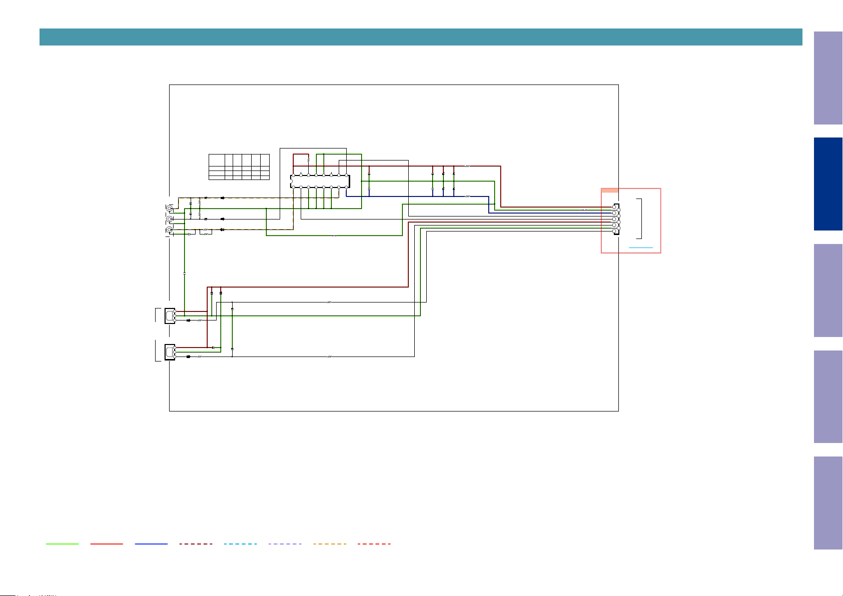
SCH08_VIDEO, OPTICAL INPUT
VIDEO /O PTICA L PART
Before Servicing
This Unit
CO MP OS ITE IN/ OU T
CB L/SAT IN
M EDIA PLAYER IN
M ON ITOR O UT
MEDIA PLAYER
TV
O PTIC AL RX 1/2
JK781
CJJ4S063ZD
JK782
CJSJSR 1124
JK783
CJSJSR 1124
OPT1 OPT2
NLM 2595 S/W TAB LE( SW2 ,5 CO NTR OL)
FU NC.IN
MUT E
MED IA
PLAY ER
CBL/ SAT
C7805
10/50V
PEN
R7804
O
75(1% )
C7803
OPEN
C7804
C7802
R7803
75(1% )
10/50V
R7801
1.8K
C7801
R7802
22pF
82(1% )
0.1uF
C7714
0.1uF
C7813
C7812
321
VCC
RX
GND
R7809
OUT
33
321
VCC
RX
GND
OUT
C7715
0.1uF
R7811
33
SW 3
SW 1
SW 2
(14)
(10)
FIX F IX F IX
L
X
H
L
H
X
X
H
H
100/50V
33PF
C7814
33PF
C7815
SW 4
SW 5
(6)
(4)
(2)
L
L
(L)
L
H
(L)
L
H
(L)
10K
R7806
VO2
VIN1
SW1
VCC
16 15 14 13 12 11 10
IC781
NJM2595MT E1
V01
SW5
SW3
VIN5
R7807
VO3
VIN2
SW2
GND
9
C7806
0.1uF
87654321
C7807
0.1uF
VSS
VIN3
VIN4
SW4
J7805
OPEN
R7810
33
R7812
33
C7808
C7809
270(1W)
Z5.1V
OPEN
D7801
C7810
10/50V
Z5.1V
OPEN
D7802
C7811
10/50V
R7808
270(1W)
J7806 OPEN
CN781
CN781
1.+12V
1
2.VGND
2
3.-12V
3
4.CVB S_SW 2
4
5.CVB S_SW 5
5
6.+5V D
6
7.OPT 1_IN
7
8.DGND
8
9.OPT 2_IN
9
DS P PAR T
TO DIGI TAL B 'D
TO CN741
Electrical Mechanical Repair Information Updating
GND LINE
POWER+ LINE
POWER- LINE
AUDIO SIGNAL
DIGITAL AUDIO
TMDS SIGNAL
ANALOG VIDEO
STBY POWER
16
Page 17
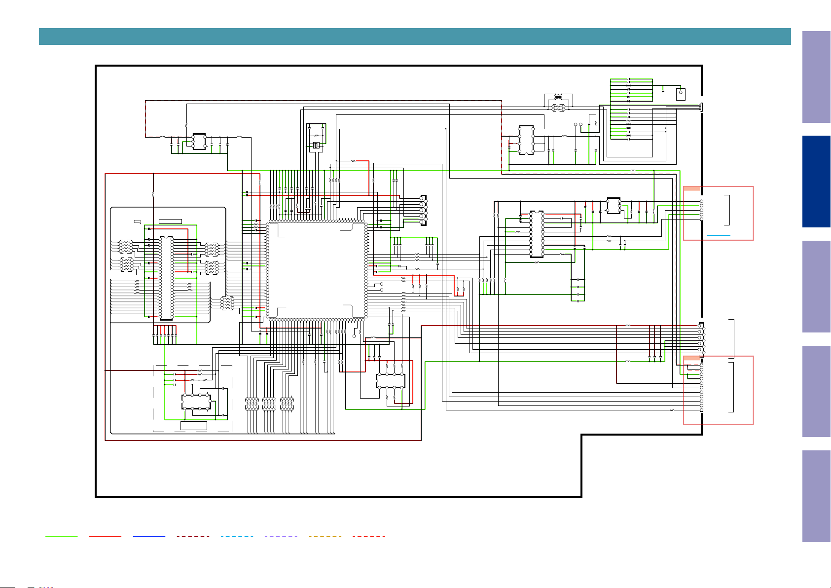
SCH09_USB, BT
USB / BT PART
D0
D1
D2
D3
D4
D5
D6
D7
LDQM
WEN
CASN
RASN
SDCSN
AD13
AD14
AD10
AD0
AD1
AD2
AD3
Before Servicing
This Unit
0.1uF
C9124
0.1uF
C9125
D9014
CDS3C05HDMI1
OPEN
C9107
C9029
0.1uF
CHASSIS
10uF
IC910
BU33TD3WG
5 1
VOUT
4
NC
KDS160
D9010
D9011
KDS160
C9037
OPEN
C9030
0.1uF
C9010
6.3V/220uF
2.2K
R9012
D9015
CDS3C05HDMI1
D9013
CDS3C05HDMI1
C9032
OPEN
D9012
CDS3C05HDMI1
C9031
OPEN
METAL PLATE
CJJ9X010Z
JK91
4.DGND
4321
3.USBD+
2.USBD-
1.VBUS
Electrical Mechanical Repair Information Updating
L9023
CB03YTYH600
BN914
BN914
VIN
2
GND
3
STBY
470
470
C9026
2200pF
L9019
CB05YTYH221
L9024
CB03YTYH600
10uF
10K
L9025
C9022
C9103
R9093
OPEN
0.1uF
C9027
2200pF
C9019
10uF
0.1uF
C9058
C9085
1000pF
R9092
1
1.+5VA
2
2.DA_GND
34
3.USB/BT_R
4.DA_GND
5
5.USB/BT_L
TO DIGITAL B'D
WIRE/5P/2.0mm
TO CN752
CN911
1
1.VDD
2
2.RESET
3
3.RTS
4
4.CTS
5
5.TXD
6
6.BT_GND
7
7.RXD
8
8.BT_GND
9
9.I2C_SCL
10.I2C_SDA
10
BN912
BN912
1
1.D5V
23
2.D5V
3.DGND
4
4.DGND
56
5.USB3V3
6.USB_POWER1
7
7.BT_TX
89
8.BT_RX
9.BX_RST
10.USB_DAC_MUTE
1011
0
11.USB_EN
DIGITAL POWER PART
TO BT MODULE
MCU PART
TO DIGITAL B'D
WIRE/11P/2.0mm
TO CN713
L9022
IC905
CVIBD82065FVJ-E2
4321
EN
IN
IN
GND
DVDD
DGND
LDOO
XSMT
FMT
LRCK
DIN
BCK
SCK
FLT
/OC
OUT
OUT
8 7 6 5
OUT
IC906
CVIPCM5100APWR
16 17 18 19 201413
15
11 12
R9090
OPEN
43
21
RN909
0x2
T9001
T9002
0.1uF
100
R9073
C9060
L9011
CB05YTYH221
1uF
0.1uF
C9059
C9033
CPVDD
123456789
C9035
CAPP
2.2uF
CPGND
CAPM
VNEG
OUTL
OUTR
AVDD
C9054
AGND
R9028
DEMP
10
10K
0
0.1uF
0.1uF
C9028
C9100
OPEN
C9013
0.1uF
C9056
C9021
0.1uF
C9055
2.2uF
C9036
R9060
0.1uF
R9061
10uF
C9020
C9121
0.1uF
C9120
0.1uF
C9122
0.1uF
C9128
0.1uF
D5V
15pF
C9087
C9086
12.0MHz/10pF
C9079
10uF
0.1uF
C9017
C9041
L9014
10uF
0.1uF
C9016
C9044
CB05YTYH221
119
118
117
116
115
IVSS33
USB_D-
USB_D+
USB_VDD33
USB_VSS33
IC901
BX8804
USB DECORDER
LDQM
UDQM
BA14
SDCSN
VDD12
434241
45
44
46
0.1uF
C9043
220
R9034
LDQM
UDQM
SDCSN
15pF
R9033
1M
X9001
10K
R9088
1k
100K
100
OPEN
1000pF
R9032
R9087
R9086
R9071
560
R9066
C9064
0.01uF
111
114
113
112
110
109
108
XI
XO
TEST
IVS33
NTRST
RESET
VDD33
CKE
RASN
VSS33
CASN
VSS12
SDCLK
VDD33
47
48
50
49
52
51
53
220
220
0.1uF
R9037
R9036
C9061
220
R9035
10pF
C9069
CKE
RASN
SDCLK
CASN
WEN
97
99
98
107
106
105
104
103
102
101
100
VSS12
NCNCNC
NC
NC
VDD12
TDI
NC
BD82065_OC
BD82065_EN
NC
97.TDO
100.TCK
99.TMS
98.TMS
NC
NC
NC
NC
NC
I2S_LRCK
I2S_BCK
I2S_MCLK
VSS33
VDD33
I2S_DATA
NC
NC
BT I2C_SCL
BT_I2C_SDA
NC
NC
NC
USB_TX
USB_RX
BT_RST
BT_RTS
61.NC
63.FLASH_CS
64.FLASH_CLK
62.NC
BT_CTS
BT_RX
BT_TX
FLASH_DI
FLASH_DO
WEN
GND
CP_SDA
CP_RESET
NC
NC
CP_SCL
54
55
57
56
59
58
60
62
61
64
63
0
47
47
100
470
R9050
T62
R9042
R9041
R9074
R9078
OPEN
OPEN
R9039
R9040
9695949392919089888786858483828180797877767574737271706968676665
CB05YTYH221
C9023
SERIAL FLASH
220pF
220pF
10K
R9023
C9088
C9089
for DEBUG
CN913
1
1.VCC
2
2.NTRST
3
3.TDI
4
4.TCK
5
5.TMS
6
6.TDO
7
7.RESET
C9078
1000pF
C9098
0.1uF
C9090 33pF
C9093 OPEN
C9039
0.1uF
C9077
1000pF
R9048
R9049
T75
T74
R9052
R9051
R9072
R9047
R9046
R9075
R9076
OPEN
OPEN
C9038
C9057
L9013
10uF
C9095
C9076
0.1uF
1000pF
10K
R9077
R9069
CLK
VCC
HOLD#
IC904
CS#DOWP#
1
2 3 4
EN25QH16B104HIP2A
47
R9068
R9043
8
8.DGND
9
9.DGND
OPEN
OPEN
OPEN
C9092 33pF
C9091 33pF
47
R9045
5678
10K
C9008
C9006
C9007
100
R9018
100
R9019
100
R9020
C9009
33pF
R9010
47
47
47
10K
10K
10K
R9022
R9067
R9044
470
470
1k
47
47
0
0
47
DI
VSS
10K
10K
R9079
R9080
1uF
C9034
10K
OPEN
C9052
0.1uF
C9053
R9026
R9025
0.1uF
R9017
0
0
OPEN
OPEN
OPEN
OPEN
OPEN
L9029
R9065
R9064
R9024
R9062
R9063
100
R9089
IC909
L9026
CB05YTYH221
BU12TD3WG
51
VOUT
VIN
2
GND
10uF
3
4
NC
STBY
C9110
C9109
0.1uF
L9027
CB05YTYH221
10uF
0.1uF
C9113
C9112
C9111
16V/10uF
USB1V2
USB3V3
L9010
0.1uF
C9096
C9080
1000pF
C9018
C9075
4 3 2 1
8
AD8
10uF
L9015
10K
10K
10K
0.1uF
C9042
10uF
C9015
CB05YTYH221
R9083
R9084
R9085
128
127
126
125
124
122
123
121
120
ADIN1
ADIN0
AVDD33
AVSS33
PLL2_VDD12
PLL2_VDD12
PLL2_VDD12
PLL2_VSS12
PLL2_VSS12
PLL2_VSS12
NC
NC
D0
D8
128.ADIN2
126.ADIN4
127.ADIN3
9 8 7 6 5 4 3 2 1
D1
D9
D2
D10
D3
VDD12
VSS12
NC
D11
D4
D12
D5
D13
D6
D14
D7
D15
ADO0
ADO1
ADO2
35.AD7
33.AD5
34.AD6
VDD33
VSS33
ADO3
ADO4
AD9
AD10
AD11
AD12
AD13
AD8
3231 3029 2827 2625 2423 2221 2019 1817 1615 1413 1211 10
33
34
36
35
38
37
39
40
1000pF
4 3 2 1
33x4
7 6 5
8
7 6 5
RN908
AD14
AD11
AD12
AD13
AD9
AD10
CB05YTYH221
C9012
6.3V/47uF
L9018
CB05YTYH221
+3.3V
SDRAM 64Mbit
C9014
16V/10uF
IC902
RN901
33x4
4 3 2 1
4 3 2 1
RN902
33x4
R9053
R9055
R9056
R9057
W9864G6KH-6
C9045
0.1uF
7 6 5
8
7 6 5
8
470
470
470
470
470
C9049
0.1uF
VSS
54535251504948474645
VDD
DQ15
DQ0
C9046
VSSQ
VDDQ
0.1uF
DQ14
DQ1
DQ13
DQ2
C9051
VDDQ
VSSQ
0.1uF
DQ12
7 6 5 4 3 2 1
DQ3
DQ11
8
DQ4
C9047
VSSQ
9
VDDQ
0.1uF
DQ10
DQ5
DQ9
DQ6
4443424140393837363534333231302928
C9050
VDDQ
VSSQ
0.1uF
DQ8
DQ7
C9048
VSS
VDD
0.1uF
NC
LDQM
/WE
/CAS
/RAS
/CS
BA0/A13
BA1/A14
A10/AP
A0
A1
A2
A3
VDD
2726 2524 2322 2120 1918 1716 1514 1312 1110
0.01uF
0.01uF
0.01uF
C9067
C9065
C9066
470R9054
R9059
UDQM
UDQM
220
R9038
SDCLK
CLK
R9058
470
CKE
AD12
AD12
AD11
A11
A9
A8
A7
A6
A5
A4
VSS
0.01uF
1000pF
1000pF
1000pF
C9068
C9082
C9083
C9084
C9094
C9062
C9063
47pF
0.1uF
0.1uF
IC903
23671011050AS_DM
Apple Auth.
R9029
R9030
R9031
10K
8 7 6 5
VCC
RST
GND
SDA
2.0c
AD9
AD8
AD7
AD6
AD5
AD4
10K
10K
R9070
1k
SCL
NC
C9011
6.3V/220uF
C9081
1000pF
10K
R9081
10K
R9082
C9097
0.1uF
RN903
33x4
D0
D8
D15
D1
D14
D9
D13
7 6 5
D2
D12
8
4 3 2 1
D10
D3
C9040
D11
0.1uF
D10
C9072
D9
7 6 5
1000pF
D11
D8
8
4 3 2 1
D4
RN904
D12
33x4
D5
D13
D6
CKE
D14
D7
D15
AD0
AD1
AD2
7 6 5
AD3
NC
9
NC
4321
C9099
8
4 3 2 1
0.1uF
RN905
33x4
C9073
1000pF
C9074
1000pF
CP_SDA
CP_SCL
C9071
OPEN
C9070
OPEN
4321
33x4
33x4
8
765
RN906
RN907
AD7
AD6
AD4
AD5
GND LINE
POWER+ LINE
POWER- LINE
AUDIO SIGNAL
DIGITAL AUDIO
TMDS SIGNAL
ANALOG VIDEO
STBY POWER
17
Page 18
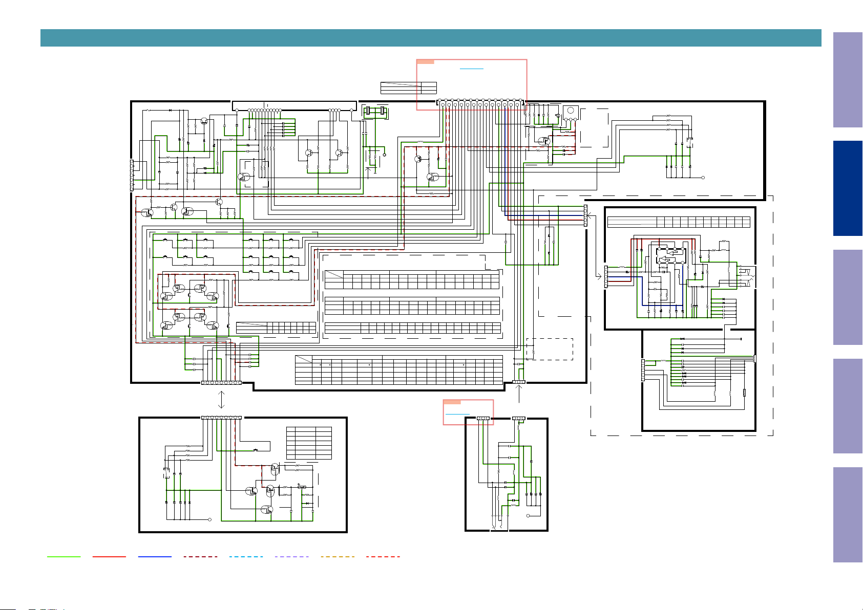
SCH10_FRONT
7. FL _AC
6. NC
5. FL _AC
4. NC
3. GND
FRO M TR ANS
2. NC
1. V DISP
2.5 mm 7PIN WAF ER
FRONT P A RT
F1001
D1001
T 200mA L 250V
1N4007SL
R1001
1.8(A XIAL )
R1002
OPEN (AXIA L)
OPEN
C1001
R1003
OPEN (AXIA L)
1 2 3 4 5 6 7
CN102
CJP07GB 03ZY
R1004
1.8(A XIAL )
2SC3052
Q1016
220K
R1428
R1429
Q1015
10K
R1430
KRC104S
SW102
SW108
R1091
RED_ LED
W/G_ LED
Q1017
KRC102S
Q1021
KRC102S
CUP 12957Z-3
VR102
CSR2A 060Z
C
12CL ICK
EN CO DE R
FU NCTIO N
(SMALL)
Before Servicing
BN12B1
*O PTIO N
27PIN
AVR-S640H /AV R-S740H /AVR -X1500H
FL101
CFL18BT 021GINK
F2
NP
CSCPDA
VFL
OSC
VDD
GND
VDDH
C1007
100V/0.047u F
C1010
C1011
Q1002
OPEN
TR OPT ION
C1088
C1089
C1090
C1091
9. PO WER_ KEY
9. PO WER_ KEY
C1009
47/16V
(SMALL)
0.1uF
KRC102S
SW105
R1073
150
SW111
R1078
100
SW117
R1083
150
AVR-S640H/ AVR- S740H/A VR-X 1500H
OTHER
OPEN
OPEN
OPEN
OPEN
ON/ STAN DBY
SW101
Q1009
KRC102S
0.1uF /50V
R1068
RESET
C1012
C1013
C1014
10(AXIA L)
C1015
C1016
R1067
100
100
100
100
R1012
R1013
R1014
R1015
39K
10K
OPEN
R1010
R1011
SW106 SW107
R1074
100
SW112
R1079
0
SW118
R1084
100
*O PTIO N
Q1017 Q1018 Q 1019 Q1020 Q1021 Q1022 Q1023
O O O O O O O O
OPEN OP EN OP EN O PEN
Q1008
KRA102S
Q1011
KRA102S
Q1012
KRC102S
Q1001
KTC1027Y T
OPEN
C1423
Z39V
10(AXIA L)
D1005
C1004
50V/1u F
C1003
R1423
220
10/50V
47K(AX IAL)
(SMALL)
D1003
Z6.8V
220
Q1014
KTC1027Y T
1W/10
R1425
R1426
SW104
R1072
OPEN
SW110
R1077
150
R1090
OPEN
Q1019
Q1020
R1082
KRC102S
R1092
OPEN
Q1023
Q1024
KRC102S
2. ISE L_A
3. ISE L_B
1. +3 V3
4. DGND
5. DGND
1 2 3 4 5 6 7 8 9
2.0 mm 9PIN WIRE
2.0 mm 9PIN WIRE
1 2 3 4 5 6 7 8 9
1. +3 V3
4. DGND
5. DGND
2. ISE L_A
3. ISE L_B
6. W/ G_LE D 6. W/ G_LE D
LUG1 4
OPEN
CHASSI S
OPEN
R1030
1W/10
R1427
180
OPEN
R1081
SW114
7. RED _LE D
8. MC U+5
8. MC U+5
7.RED _LED
R1007
R1062
10K(AX IAL)
27K(1/ 4W)
100uF/63V
C1006
50V/1u F
C1005
R1424
220
R1006
R1009
C1002
100V/0.1 uF
220
R1005
R1008
Q1013
22K
KRC102S
SW103
R1071
OPEN
SW109
R1076
OPEN
EN
OP
Q1018
KRA102S
KRA102S
SW115
Q1022
KRA102S
KRA102S
SW116
OPEN
C1087
OPEN
C1086
OPEN
C1085
BN101_1
BN101
R1413
10K
R1414
10K
R1415
1K
R1416
1K
AB
0.01uF
0.01uF
C1426
C1425
OPEN
OPEN
OPEN
OPEN
OPEN
C1427
D1406
C1429
C1428
D1407
TSA
TSB
434 4454 6474 8495 0515 25357
OPEN
100P
100P
330P
1000P
AVR-X 250BT
AVR-S 540BT/ X550BT
Q1002 OPE N
R1011 OPE N
R1068 0
AVR-S 640H/A VR-S740H /X1500H
Q1002 KRC 102S
R1011 10K
R1068 OPE N
R1075
0
KEY1
SW113
R1080
0
KEY2
SW119
R1085
0
KEY3
OPEN OPEN OPEN
OPEN
KE Y NAME
AVR-S 540BT
AVR-X 250BT
AVR-X 550BT
AVR-S 740H
AVR-X 1500H
AVR-S 640H
LED OPT ION
AVRX 1500H E3
D1012
WHIT E/RE D
R1041
R1042
R1043
R1044
D1002
R1041
R1042
D1012
CVDP VBW R5A2 M
R1043
R
4.7K
R1044
OPEN
C1054
0.1uF
NX
2SC3052
Q1003
39K
R1025
+3V3
Q1024
SW102 SW 110 SW111
ADJUS T
PURE
PURE
1K2
1K2
4K7
OPEN
1SS133M
1.2K
1.2K
W/G
R1045
OPEN
D1002
1SS133M
C1055
NP
Q18G
17G
18G
Q17G
100
R1018
R1019
2SC3052
Q1004
39K
100K
R1017
R1016
R1026
*O PTIO N
AV R-S540BT /X550B T/X 250BT R ESIST OR V ALUE
AVR-S 540BT
5.6K
AVR-X 550BT
OPEN
AVR-X 250BT
AV R-S740H /X1500H /S640H R ESIST OR V ALU E
R1071
AVR-S 640H
330 220 180
AVR-S 740H
OTH ER
OPEN
KE Y OP TION
AVR-S 540BT/ S740H/S 640H
OTH ER
KEY_ 1 KEY_ 2 KEY_ 3
ADJUS T
PRESE T-
TUNE +
-
STAT US
TUNE -
-
GAME
TUNE +
PRESE T-
--
STAT US
Z2 ON /OFF
TUNE -
MOD E
GAME
OTH ER
GREEN/R ED
1K2
1K2
4K7
OPEN
OPEN
SB-LE D
0.1uF
AVR-X250B T/A VR-S540B T/A VR-X 550BT
PCB B RAK ET
BK101
BK102
F1
1 2
1 2
15678
3 4
3 4
CMD1A572
CMD1A572
OPEN
100V/0.047u F
C1041
C1017
100
100K
BN10
OPEN
OPEN
OPEN
R1086
R1087
STY LE PI N
CHGND
BRACKE T
Op tion
AVR -X1500H E 2/E1 C/K
ON LY
KEY_ 1
KEY_ 2
KEY_ 3
R1076
1K
1.5K
2.7K
3.3K
1K
1.5K
OPEN
0
OPEN
R1076
R1075 R1078
R1074
R1073
330 220
150
100
OPEN
Z2 ON /OFF
OPEN
150
0
100
SW102 SW 103 SW104 SW105 S W106 SW107 SW 108 SW109 SW 110 SW111 SW 112 SW113 SW 114 SW115 SW116 SW 117 SW118 SW 119
O
O O O O O O O O O O O O O O O O O
OPEN
OPEN
O O O
SW107SW105 SW114SW103 S W104 SW106 SW 113SW108 SW116SW115SW112SW109
ON/O FF
Q/S_ 1
SOUN D
PRESE T-
-
-
MOVI E
Q/S_ 1
-
PRESE T-
-
PRESE T-
MOVI E
Q/S_ 1 Q/S_ 4
NET_FA CT_ RST
N.C
BN12B1
CJP27GB 286ZN
L1001
CB03YT YH 600
R1021
Q1005
ISA1530AC 1
R1020
+3V3
R1422
R1079 R1080R1077R1072 R1074 R1075 R1078R1073R1071
1.5K
2.7K3.3K5.6K 2.7K3.3K5.6K
1.5K
1K
KEY_ 2KEY_1
R1079
180 150 100
150 100
0 0
OPEN O PEN OPEN OPEN OPEN OPEN
O O O O O O O
PRESE T+
PRESE T+
TUNE +
Z2 SE L
TUNE +
Q/S_ 4
STAT US
SLEEP
Q/S_ 4
Q/S_ 2
MOD E
STAT US
Q/S_ 4
Q/S_ 4
Q/S_ 2
STAT US
SLEEP
EN CO D ER &P OW E R
27.NET_ FACT _RST
26.DGND
25.MCU_3V 3
27
1K
C1019
C1020
50V/10uF
3.3K
Q1006
KRC102S
OPEN
1K
OPEN
00
R1080R1077R1072
R1081
330 220 180
OPEN
Q/S_ 2
TREBLE
MUSIC
Q/S_ 2
MUSIC
Q/S_ 2
2.0 mm 3PIN WAF ER
CN104
TO BN505
TO CN711
FRO M DI GITAL B'D
1.25mm 27PIN FFC
15.KEY _1
22.FL_D ATA
20.FL_C E
24.MCU_5V
16.RED_ LED
21.FL_C LK
18.RC_IN
19.FL_R ST
23.CPU_ POW ER
17.W/G _LED
1517
1921
2325
16318
2022
2426
0.01uF
KEY_ 3KE Y_2KEY_ 1
R1084 R1085
R1083R1082R1081
1K
1.5K
0
1.5K2.7K
1K
KEY_ 3
R1082
R1085R1084
R1083
100
150
150 100
0
180
BASS/
MOD E
TUNE -
SOUN D
-
DIMMER
PRESE T+
Q/S_ 1
TUNE -
Z2 SE L
BAND
Q/S_ 1
-
DIMMER
PRESE T+
PRESE T+
INFO
BAND
TO MAIN
3.HP_ LCH
CN104
CUP 12957Z-4
13.KEY _3
14.KEY _2
R1090 R1092
R1090
OPEN
OPEN
2.AGND
1.ISEL _A
4.POW ER_ KEY
6.-12V
9.B/P _IRIN _DE
8.AGND
3.MIC _DET
5.+12V
7.MIC _SIGNAL
2.ISEL _B
11.VSEL _A
12.VSEL _B
10.H/P _DET
1011121314
AVR X1500H E3 ON LY
12456789
390
390
R1418
R1419
OPEN
R1069
R1022
Op tion
47K
R1420
Q1007
KRA102S
1K
RC101
38KHZ
OPEN
OPEN
C1430
D1408
R1023
(38kHz )
OPEN
Op tion
Vcc
GND
VOUT
AVR-X 250BT
LD101
321
AVR-S 540BT/ X550BT
R1421
47K
Q1007 OPE N
R1022 OPE N
R1023 OPE N
R1069 1K
AVR-S 640H
R1024
OPEN
AVR-S 740H/X 1500H
Q1007 KRA 102S
R1022 1K
R1023 47K
R1069 OPE N
R1053
10
C1038
47/16V
(SMALL)
C1039
100P
+3V3
D_GND
VOL-
VOL+
R1061
10K
10K
R1060
1K
R1059
R1058
1K
A B
0.01uF
0.01uF
VR101
CSR2A 055Z
C
C1077
C1076
VO LU ME
24CL ICK
OPEN
0.1uF
OPEN
OPEN
C1074
C1073
D1015
D1016
EN CO DE R
OPEN
(SMALL)
C1075
LUG1 1
CHASSI S
WIRE
CUP 12957Z-1
1. AGND
12345
BN12A
2. MIC _SIGNA L
3. -12V
4. +12V
5. MIC _DE T
Z5.1V
47K
OPEN
AVR -X250BT
OPEN
R1046
2.DGND
1.DGND
123
CN103
2.0 mm 3PIN WAF ER
2.0 mm 3PIN WIRE
2.DGND
1.DGND
123
L1011
CB03YT YH600
C1084
OPEN
1/50V
1/50V
0.1uF
0.1uF
C1065
C1067
C1068
C1066
LUG1 3
CHASSI S
WIRE
H EAD PHO NE
D1403
C1409
R1410
Z5.1V
D1402
AVR -S540BT /X550BT
ON LY
OPEN
C1082
0
0
00
R1092
OPEN
OPEN
SW119SW118SW117
C1081
Q/S_ 3
DIMMER
0.1uF
-----
Q/S_ 3
DIMMER
Q/S_ 3
3.H/ P_DE T
Q/S_ 3
-
DIMMER
Q/S_ 3
1.HP_ RCH
3.H/ P_DE T
123
BN131
C1424
0.1uF
C1069
OPEN
470
R1057
L1010
C1071
CB03YT YH 600
680P
C1072
680P
C1083
L1012
OPEN
CB03YT YH 600
L1013
CB03YT YH 600
18732
87321
CJJ2E041ZD
JK104
2. HP _LCH
3. HP _RCH
8. DGND
7. DE T
1. AGND
* O PTIO N : R ESIS TO R & CAP VA LUE
AVR-S 540BT/ AVR-X 550H
AVR-S 640H/A VR-S740H /AV R-X1500H
0.1uF
1/50V
C1411
2.0 mm 5PIN WIR E
2.0 mm 5PIN WIR E
BN12B
C1417
L1403
CB03YT YH600
1. AGND
12345
C1452
R1433
2. MIC _SIGNA L
50V/10uF
3. -12V
4. +12V
5. MIC _DE T
CU P12957Z-2
AV R-X250B T N OT US ED
100
TO DIGI TAL B OAR D
2.0 mm 5PIN USB WI RE
R1401 R1435R1408 R1409 C1408R1407 R1437R1434 C1450R1436 C1406
R1027
OPEN
56K
820
56K
4K7
100
1K
V+
8
7 6 5
(SMALL)
CM1
IC101
NJM4580CG
OPEN
O
R1435
R1434
10K
R1436
C1450
OPTIO N
33p
R1408
33K
C1408
33P
10K
100
R1027
R1407
R1409
100K
R1432
C1407
C1451
100/16V
(SMALL)
50V/100pF
BN104
L1404
CB03YT YH600
5.DGND
4.DGND
3.USB D-
2.USB D+
1 2 3 4 5
1.VBU S
CU P12957Z-5
AV R-X250B T S540B T/X550B T NO T US ED
AV R-S640H /AVR -S740H/ X1500H U SE
0
33K
10K
100
10K
+-O
2.2K
OPEN
CM2
0.1uF
R1412
R1411
4321
V-
+
100
R1406
C1405
10/50V
(SMALL)
OPEN
R1437
C1402
1/50V
(SMALL)
1K
100K
100P
OPEN
(SMALL)
10K
R1431
1/50V
C1406
C1410
C1404
C1403
R1404
0.047uF
D1008
CDS3 C05HD MI1
0.1uF
C1053
D1020
KDS160
D1019
KDS160
OPEN
C1051
0.1uF
C1050
220/10V
C1052
(SMALL)
R1040
2.2K
CDS3 C05HD MI1
D1011
CDS3 C05HD MI1
D1010
OPEN
C1049
CDS3 C05HD MI1
D1009
OPEN
C1048
OPEN
OPEN
0
27P
0.1uF
0.047uF
OPEN
C1401
Z5.1V
D1401
33P 33P
00OPEN
R1054
OPEN
R1401
L1401
CB03YT YH 600
100
100K
R1402
MICD ET
1
2.2K
7
6
L1402
CB03YT YH600
3
MIC
MIC
2
R1405
4
5
CJJ2D049ZD
JK105
KDS160
D1404
KDS160
D1405
100K
C1413
OPEN
C1414
0.1uF
C1415
1000P
R1403
C1416
OPEN
JAC K IN : SW OPEN
CHASSI S
META L PLA TE
JK101
4.DGND
3.DA TA+
1 2 3 4
2.DA TA-
1.VBU S
0
0
L1003
L1005
L1004
iP OD /U SB
CB08YT YH 600
This Unit
Electrical Mechanical Repair Information Updating
GND LINE
POWER+ LINE
POWER- LINE
AUDIO SIGNAL
DIGITAL AUDIO
TMDS SIGNAL
ANALOG VIDEO
STBY POWER
18
Page 19
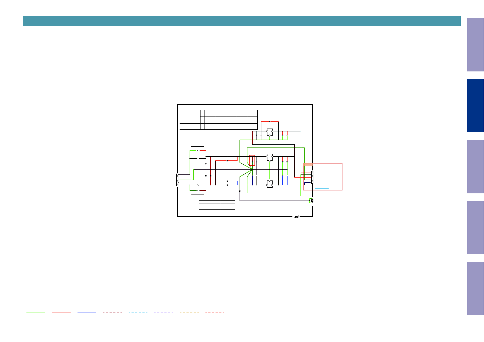
SCH11_REGULATOR
Before Servicing
This Unit
REGULATOR PART
FRO M TR ANS
1.AC _S2
3.RT N_GND
5.AC _S2
2.NC
4.NC
CN302
12345
FUS E OP TION
AVR -S740H/ X1500H
AVR -S540BT /S640H
AVR -X250BT /X550B T
MOD EL
FU SE O PTIO N
T 1.25A L 250V
T 1.25A L 250V
F3004
F3002
OPEN
F3001
OPEN
F3003
Ver
E3
E2
E1C
K
ALL
AC120~ 230V
C3004
C3003
MOD EL
AVR -S640H
AVR -S740H/ X1500H
AVR -S540BT /X550BT
AVR -X250BT
AC
AC120V
AC230V
AC220V
AC100V
OPEN
OPEN
C3005
0.1uF (M)
OPE N OPEN
218Seri es
OPE N OPEN
D3001 UF4004
D3002 UF4004
D3003 UF4004
D3004 UF4004
C3006
25V/6800uF
25V/4700uF
F3002F3001 F3003 F 3004
932Seri es 932Se ries
218Seri es
OPE N OPEN
932Seri es 932Se ries
OPEN
C3024
Electrical Mechanical Repair Information Updating
D3101
OPEN
IC305
CVIKI A7805BPI
IN
OUT
123
GND
OPEN
C3001
OPEN
C3002
IC301
CVIKI A7812BPI
IN
OUT
123
GND
OPEN
C3006
C3010
4700/25V
OPEN
C3007
C3011
3300/25V
GND
IN
OUT
213
IC302
HVIK IA7912PI
OPEN
OPEN
C3008
C3009
D3108
470/50V
OPEN
C3014
C3012
D3103
470/50V
1SS133MT
C3013
C3015
D3104
470/50V
1SS133MT
BN301
BN301
5.D A+5 V
OPEN
BK303
CMD1 A387
BRAC KET
4.VGND (RE T_GND)
3.+ 12V
2.RL Y_GND
1 2 3 4 5
1.-12V
TO CN771
BK301
CMD1 A569
BRAC KET
TO DIGI TAL B 'D
2mm 5 PIN W IRE
INP UT/V OLU ME PA RT
Bra cke t
No connec tion
GND LINE
POWER+ LINE
POWER- LINE
AUDIO SIGNAL
DIGITAL AUDIO
TMDS SIGNAL
ANALOG VIDEO
STBY POWER
19
Page 20
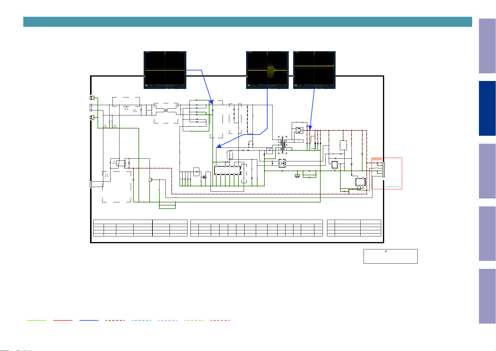
SCH12_SMPS
Before Servicing
This Unit
OP TIO N
CY601
CY602
400V/470pF
!!
!
C6001
250V/0.01u F
!
F6002
AVR -S740H/ X1500H
AC100~ 120V T 6.3A L 250V
AC220~ 230V T 3.15A L 250V
AVR -S540BT /X550BT /X250B T
AVR -S640H
AC120V T 5A L 250V
AC220~ 230V T 2.5A L 250V
OP TIO N
AVR S740H/X 1500H
AC
AC120V
AC220~ 230V
AC100V
AC100~ 120V T 2A L 250V
AC220~ 230V T 1.6A L 250V
F6001
!
400V/470pF
1
324
RY601
HF36FD /5-H LT
F6001 F 6002
2A L 250V
1.6A L 250V
2A L 250V
*O PT ION
8.2M
8.2M
R6027
R6029
!
CX601
0.1uF ,275V
8.2M
8.2M
LF602
R6030
R6028
E3,K :LF-4 ZB-E273H
E2,E 1C:L F-4ZB -E503H
D6009
1SS133MT
C6021
Q6003
50V/0.1 uF
CVT2 SC3052
R6024
10K(1608)
C6022
6.3A L 250V
3.15A L 250V
6.3A L 250V
OPEN
J6014
OPEN
J6015
OPEN
AVR S540BT/ X550BT /X250B T/S640H
F6001 F6002
2A L 250V
1.6A L 250V
-
BK602
BRAC KET
CMD1 A834
12
YAW 396-NNV
CN601
BK601
BRAC KET
CMD1 A834
CN602
YW396-NNB
12
TO POW ER T RANS
OP TIO N
Ver Ver
E3
E1C /E2
K
R6025
4.7K( 1608)
5A L 250V
2.5A L 250V
C6002 250V/0.01u F
D6001 1N 4007
D6002 1N 4007
OPEN
D6003 1N 4007
CX602
D6004 1N 4007
D6005 1N 4007
D6006 1N 4007
J6002
JUMPE R
C6003
250V/0.01u F
1
R603
1M(2125)
R6032
1M(2125)
R6033
1M(2125)
*O PTIO N
OPEN
C6009
50V/0.22u F
C6007 50V/0.1 uF
R6004 330K
C6005
C6006 OPEN
*O PT ION
E1C /E2
-
*O PT ION
*O PT ION
Z22V
ZD611
Z39V
R6008
C6004
200V/100uF
J6003
JUMPE R
Q6002
ZD621
2N7002KA
Z7.5V
D
G
S
R6006
1M(1608)
ZD621
AC
E3
K
AC120V
AC220~ 230V
AC100V
ZJ7.5 B
ZJ16B
ZJ5.6 B
ZD608
Z22V
2.2M( 0.2W )
ZD612
Z39V
ZD609
Z22V
ZD613
C6011
R6009
Z39V
ZD610
Z22V
2.2M( 0.2W )
ZD614
1KV/ 1000pF (S MD)
Z22V
ZD615
Z22V
ZD616
R6010
1M(0 .2W)
Z22V
E3, K:100UF /200V
E1C ,E2 : 100UF/400V
*O PT ION
ZD601
Z12V
4 3 2 1
6
F
D
IC601
CVITO P268VG
S
S S S S S
7
9
8
ZD608 ZD 609 ZD610
ZJ39B
OPE N OPEN OPE N O PEN OPE N OP EN
ZJ39B
ZD617
R6011
10(1608)
C6026
D6012
1N4007
1KV/ 47pF
D6007
ZD618
1N4007
Z27V
270K
R6012
VXC
R6015
R6013
6.8(0 .2W)
22K(1608)
1211
10
AVR S540BT/ X550BT /X250B T, S640H , S740H /X1500H OPT ION L IST
ZJ39B
ZJ39B
*O PTIO N
C6013
C6012
R6014
1K(1608)
47/25V(N XA)
R6008 R6009 R6010 R6012
ZJ39B
2M2 (0.2W )
2M2 (0.2W )
ZJ39B
2M2 (0.2W )
2M2 (0.2W )
C6027
R6034
OPEN
OPEN
OPEN
C6028
1
2
T6001
VLT9 Z132ZW
1
2
3
4
5
D6008
6
)
UF4004
7
C6008
50V/10UF( NXA
Z39V
ZD620
400V/2200pF
0.1uF (1608)
1M( 0.2W )
1M( 0.2W )
3
D6013
RBQ30T 65A
14
J6001
13
OPEN
12
11
10
9
8
12
3 4
IC602
EL817-B
C6023
BK603
CMD1A629
BRACKE T
R6013 R6014
270K
22K
1K
56K
22K
3K
270K
22K
1K
4.7uF (1608)
C6015
C6014 0.1uF(1608)
**OP TIO N
C6024 0.1uF (1608)
R6026
OPEN (1608)
C6025 OPEN (1608)
C6004
100UF/200V
100UF/400V
100UF/200V
100/50V
R6016
56(0.2W )
C6019 5600uF/6.3V (NX A)
C6017
C6018 5600uF/6.3V (NX A)
R6017
R6018
5.6K( 0.2W ) C6020
3.3K( 0.2W )
D6010 OPEN
IC603 K IA2431AP
321
**OP TIO N
Ref N o.
LF602
C6017
E273H
503H
E273H
R6019
22K/F(1608)
0.1uF (1608)
REF
CATHO DE
ANODE
OPEN
R6023
C6029
0.1uF (1608)
AVR S640H/S 740H/X 1500H
100/50V
R6020
OPEN (1608)
6.8K/ F
R6022
CVIPS T8448NR_ A
R6021
OPEN (0.2W )
Z6.8V
ZD619
OPEN
C6010
C6030
15N(1608)
4
NC
CD
IC604
GND
VDD
OUT
2
1 5
3
AVR S540BT/ X550BT
AVR X250BT
OPE N
** IMPO RTAN T SA FETY NOT ICE.
COMP ONEN T ID ENTIF IED B Y MARK HAV E SPE CIAL CHAR ACT ERISIC S.
IMPOR TAN T FOR SAFE TY. WHE N REP LACING ANY OF TH ESE COMP ONEN TS
USE O NLY MANUFA CTUR ER'S S PECI FIED P ART S.
** THE UNIT OF RE SIST ANCE IS OH M.
K = 1000 O HM. M = 1000KOH M.
** THE UNIT OF C APAC ITAN CE IS MICRO FARA D(u F)
pF = 10 uF
** THIS SCH EMATIC DIAG RAM MAY M ODI FIED A T AN Y TI ME W ITH T HE
IMPRO VEME NT O F PER FORMANC E.
BN601
12
D5.2 V
D5.2 V
L6001
3456
M_RES ET
0
DGND
DGND
MAINPOW ER
BN601
TO DIGI TAL B 'D
DIG ITAL POW ER P ART
TO CN751
-6
Electrical Mechanical Repair Information Updating
GND LINE
POWER+ LINE
POWER- LINE
AUDIO SIGNAL
DIGITAL AUDIO
TMDS SIGNAL
ANALOG VIDEO
STBY POWER
20
Page 21
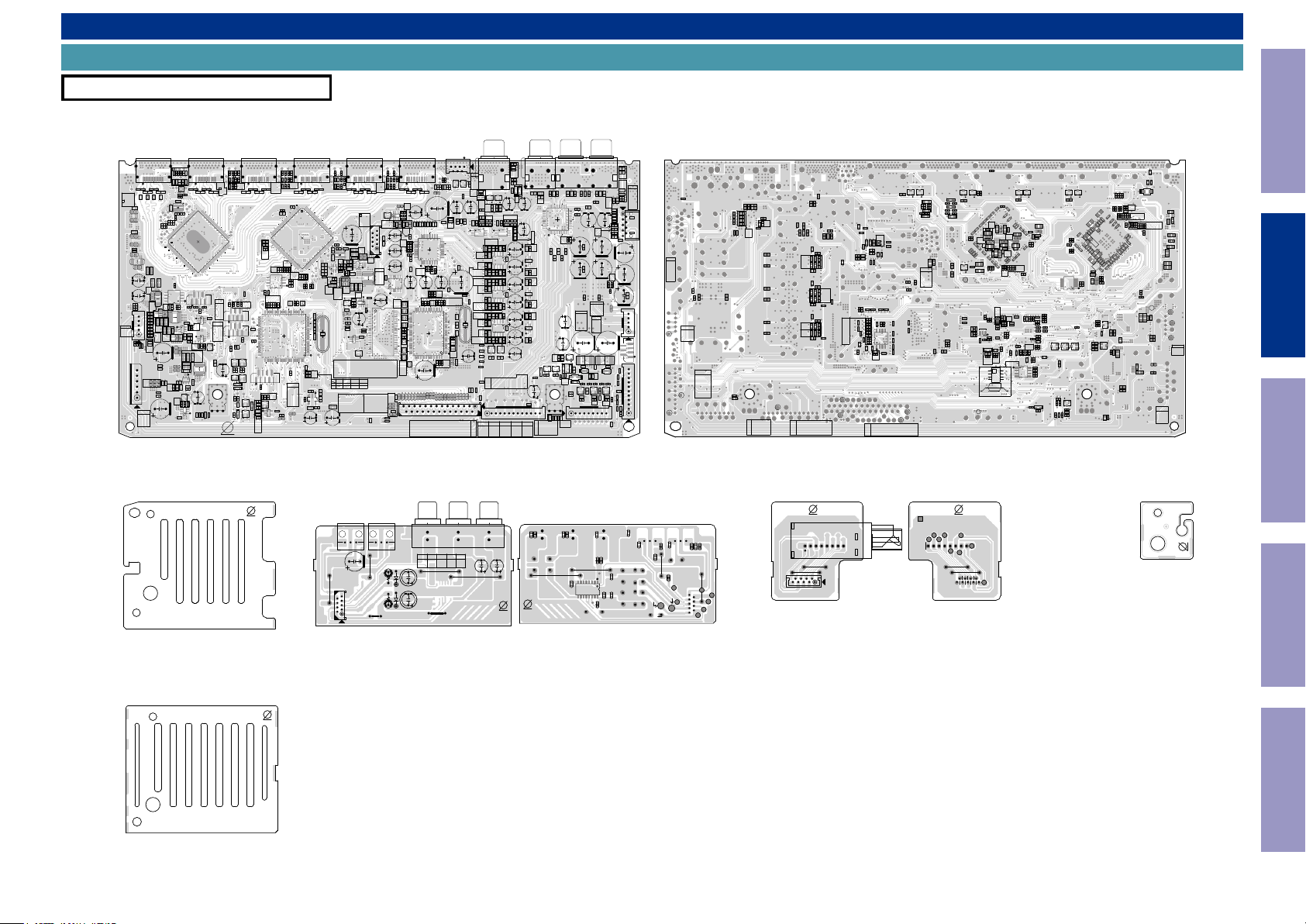
PRINTED CIRCUIT BOARDS
DIGITAL, USB WIRE GUIDE, VIDEO, TUNER, PHONE WIRE GUIDE, FRONT CABLE GUIDE
Lead-free Solder
When soldering, use the Lead-free Solder (Sn-Ag-Cu).
DIGITAL (A SIDE) DIGITAL (B SIDE)
MEDIA PLAYER
5.DA+5V
4.VGND(RET_GND)
3.+12V
2.RLY_GND
1.-12V
IN
D7322
D7321
T7226
CEC_COM
D7324D7323
R7364
R7363
R7362
R7361
D7331
D7330
RN731
RN732
A
C7341
C7340
C7339
R7367
R7366
C7358
L7305
L7301
C7361
L7306
L7308
C7356
C7350
L7302
L7303
C7344
L7309
C7365
C7396
L7310
L7307
C7367
R7145
R7772
R7148
R7773
R7147
R7722
R7759
51
CN771
CN771
R7762
R7763
C7441
C7439
C7472
C7440
C7438
CN751
L7503
L7502
L7501
1 6
CN751
6.MAIN_POWER
5.D_GND
4.D_GND
3.M_RESET
2.D5.2V
1.D5.2V
MONITOR
GAME(4K)
SCL
SDA
CEC
T7324
T7323
T7321
A
+5V
T7325
JK726
JK725
D7315
D7316
D7320
D7326D7325
D7319
UTIL
D7328
T7322
T7326
T7309
HPD
RN735
D7327
RN733
T7315
SD2
T7314
SD1
T7313
SD3
SD0
R7359
R7358
R7357
T7312
T7311
T7335
T7333
T7332
C7397
L7513
L7512
C7561
C7562
C7560
R7760
R7767
R7766
R7721
C7502
C7503
C7506
CUP12964Z_DIGITAL_MP
D7314
D7317
D7318
D7332
R7365
R7368
C7337
RN734
SDA
X731
T7328
C7338
T7331
SCL
H_MCLK
IC731
T7327
109 144
H_SCLK
10873
T7319
27MHz
T7317
T7318
R7350
H_LRCK
R7351
T7316
R7356
R7338
R7336
R7337
36
T7310
C7395
R7379
IC732
MN864788_ROM
26
4
CN731
85
7
R7384
R7396
C7399
R7381
R7398
R7397
R7382
T7337
L7511
T7336
R7383
T7339
T7338
C7524
C7558
IC752
Q7506
C7553
R7508
C7559
Q7503
L7510
L7509
C7556
C7557
C7555
R7512
R7513
R7511
R7527
R7526
C7597
Q7504
C7515
C7516
C7514
C7510
C7509
L7507
L7506
C7512
L7505
C7501
L7484
L7504
IC751
C7511
ET761
R7505
C7518
R7506
C7513
R7504
C7505
C7504
R7501
C7507
C7640
C7508
Q7509
R7534
R7533
C7527
C7742
C7641
C7733
C7743
C7732
Q7510
C7528
DIPPING
R7257
R7256
T7201
MCU UPDATE
SCL
Q7202Q7201
R7255
R7254
R7260
C7270
D7206
D7205
R7259
C7121
C7707
C7474
C7473
R7757
C7709
3217
T7404
T7403
T7402
T7401
C7734
C7735
C7453
C7615
R7417
R7416
R7411
R7410
R7409
R7413
R7407
RN743
38
C7404
R7403
C7403
R7402
RN742
RN741
128103
R7424
R7423
R7422
C7406
L7402
L7125
L7130
L7119
L7124
L7123
L7122
L7120
1020 2
4.POWER_KEY
5.+12V
6.-12V
7.MIC_SIGNAL
8.AGND
9.NC
10.H/P_DET
11.VSEL_A
12.VSEL_B
13.KEY_3
COAX IN
1267
CN716
1.RESET
2.MCU+3V3
3.TX
4.RX
5.DGND
6.N.C
7.BOOT
C7816
JK784
R7258
R7811
D7803
C7629
R7741
R7743
C7704
R7744
R7625
R7638
R7624
R7742
R7732
C7706
R7745
R7758
8
4
5
IC766
R7670
C7652
R7671
C7658
IC762
R7672
C7659
C7653
R7680
R7673
R7681
C7662
R7725
R7694
R7686
R7695
C7678
C7668
C7674
R7687
IC763
R7688
C7675
C7124
R7689
C7679
C7669
R7696
R7710
R7711 R7697
C7685
R7702
C7694
C7691
R7703
IC764
X741
24.576MHz
R7704
C7692
R7713
R7712
R7705
C7695
R7723
C7686
C7126
Q7608
C7142
C7120
R7735
C7141
C7405
C7143
C7125
CN772
C7792
C7791
C7147
L7127
L7126
C7148
FL
T7609
1 11
MI RPFCT2FCT1ICTMI RPFCT2FCT1ICT
CN711
1.ISEL_A
2.ISEL_B
3.MIC_DET
T7208
HPD
C7271
R7272
D7222
D7226
D7223
R7268
R7267
D7218D7219
D7225 D7224
D7221
D7220
Q7521
C
R7285
R7286
C7279
D7232
C7209
R7281
CN741
D7231
R7280
8 2
C7240
1 9
C7569
C7568
C7570
28.636MHz
L7515
L7514
CN741
IC753
9.OPT2_IN
8.DGND
7.OPT1_IN
C7571
6.+5VD
5.CVBS_SW5
4.CVBS_SW2
3.-12V
2.VGND
C7573
C7574
C7530
1.+12V
L7516
C7429
C7549
R7525
C7550
R7524
Q7502
C7430
C7431
C7427
Q7518
C7432
C7587
Q7517
25
BAR CODE LABEL
X550E1C
X550K
X250E1C
CUP12964Z_DIGITAL_MP
10K
10K
10K
C7803
+5V
T7207
R7273
C7591
C7520
C7801
C7444
C7437
IC745
IC743
DVD/Blu-ray
SDA
T7206
T7205
R7270
L7527
Q7522
L7508
C7468
C7802
C7470
RN749
RN748
RN751
RN750
L7101
L7102
C7122
L7104
C7793
C7149
CN716
SCL
R7269
SDA
T7202
T7203
+5V
JK721
HPD
D7209
D7210
D7213
T7204
L7403
D7214
D7212
D7207
D7208
D7211
C7454
R7557
C7459
R7558
C7590
C7455
4833
C7467
C7465
C7466
C7463
C7461
C7464
C7462
C7460
C7458
L7404
C7521
C7728
R7484
R7471
R7472
R7473
R7474
R7475
6449
R7476
C7447
16
IC744
9 16
R7478
R7193
R7479
R7477
C7451
C7423
8
C7446
R7415
R7414
R7408
IC741
6439
50
10265
26
R7418
R7430
C7434
RN747
R7419
RN744
RN745
RN746
C7442
L7105
L7116
L7115
L7114
L7113
L7112
L7111
L7110
L7109
L7108
L7107
L7106
L7117
L7103
C7123
212627
CN711
22.FL_DATA
24.MCU+5V
27.NC
25.MCU_3V3
26.DGND
23.CPU_POWER
14.KEY_2
15.KEY_1
16.RED_LED
17.W/G_LED
19.FL_RST
19.FL_RST
20.FL_CE
21.FL_CLK
CBL/SAT(4K)
BD(4K)
T7302
R7312
D7309
R7233
ADV7623 ROM
CEC_OUT
R7139
R7548
R7549
D7504
D7503
T7106
Q7113
T7301
SDA
SCL
T7304T7303
+5V
HPD
JK724
R7303
R7307
D7308
D7307
D7304
R7301
R7304
D7301
R7302
R7308
D7240
R7306
C7301
R7305
D7302
D7239
D7303
D7306
D7305
R7287
R7290
R7295
IC721
36
R7201
R7202
C7220
R7203
R7211
R7212
R7217
7237
R7206
R7210
R7209
4
C7233
R7245
R7244
R7246
T7220
HDMI_SDA
85
R7230
T7213
R7224
IC722
OSD_HOLD
R7228
C7281
C7282
R7223
R7116
R7115
RN712 RN711
R7177
R7176
R7175
R7174
R7222
R7173
T7102
R7235
R7234
CN721
73 108
T7103
T7104
C7114
R7127
109
IC711
T7108
298
R7170
Q7514
CN715
CN715
1.MCU+3V3
R7152
EMULATOR
2.DGND
3.RESET
4.JTDO
5.JTCK
C7545
R7545
R7546
6.JTMS
Q7112
7.JTDI
8.NJTRST
9.DGND
Q7512
L7521
R7541
C7551
D7502
IC755
R7547
L7129
C7543
C7578
R7544
C7544
C7788
C7542
T7306
T7305
SCL
SDA
+5V
T7307
B
1919191919 19
HPD
T7308
R7314
R7313
R7318
R7317
D7311
R7311
B
D7310
R7315
R7316
D7313
D7312
C7302
OSDTX_SCL
T7218
T7219
OSDTX_SDA
7237
T7330
T7329
OSD_MO
OSD_CS
OSD_MI
T7216
T7214
T7217
OSD_CLK
T7215
CN721
1.SCK
26
R7232
2.DGND
3.MOSI
4.VCC
5./CS
6.MISO
7.DGND
26
7
CN714
1.RESET
2.MCU+3V3
3.TX
4.RX
5.DGND
7
6.N.C
CN714
7.BOOT
MCU UPDATE
R7166
C7132
R7167
Q7513
Q7515
R7168
R7550
R7551
Q7516
C7133
T7105
R7178
R7179
C7134
R7185
D7102
Pb
MEDIA PLAYER
T7210
T7209
SDA
SCL
R7282
+5V
T7211
R7283
JK723
JK722
C
D7234
D7233
D7237
D7238
HPD
T7212
D7227
D7236
D7235
109 144
10873
R7250
R7296
R7251
X721
T7225
7623_RST
R7555
C7241
R7556
R7241
Q7520
R7240
T7224
R7238
R7239
C7588
T7222
T7223
C7285
T7221
HDMI_SCL
R7218
R7520
R7517
L7518
C7531
R7518
L7517
C7532
C7572
R7322
C7232
R7519
R7321
Q7501
R7514
C7529
37 72
C7443
C7104C7103
L7401
36
L7522
R7552
R7108
C7583
C7582
8MHz
R7107
X711
T7101
144
C7119
R7114
R7113
X550E2
S540E3
X250E2
4K7
X
R7113
10K
R7114
10K X
R7751
SET OPTION
R7750
R7746
R7749
C7746
VERSION
IC756
C7745
R7761
C7581
SW
1
1
R7627
C7702
C7703
R7765
R7764
2
JK772
5
Q7611Q7610
C7638
R7614
D7604
C7639
D7603
R7623
C7642
C7643
R7727
R7752
C7710
R7729
R7753
C7617
C7627
5240
8
4
R7678
R7679
5 8
5 8
5 8
1.FL
T7608
IC761
5
R7728
IC767
R7730
C7661
R7726
4
R7682
C7663
C7665
Q7604
C7667 C7666
C7664
4
R7719
R7698 R7683
C7682
C7680
Q7605
R7699
C7684 C7683
R7718
C7681
4
R7714
C7699
R7724
C7696
C7698
Q7606
C7697
R7715
C7700
Q7609
R7734
C7717
Q7614
D7605
C7144
R7652
C7577
11.RLY_GND
13.DGND
3.SL
5.CEN
12.MUTE_+B
2.AGND
4.AGND
6.AGND
7.SR
8.AGND
9.FR
10.+12V
T7603
T7604
SL
+12V
T7606
SR
CEN
FR
T7605
T7607
RLY_GND
T7601
DGND
CN772
C7714
T7602
MUTE_+B
131 7
CN712
1.HI-B_RLY
2.H/P_RLY
3.FRONT_RLY
4.C/S_RLY
3
41 63
42
R7622
R7619
R7621
3927
C7623
13
R7640
R7639
R7667
R7666
R7665
R7668
R7664
C7650
C7644
C7630
C7645
R7647
R7648
Q7612
Q7613
C7632
R7669
ET751
R7649
D7607
D7606
C7576
C7575
CN712
C7784
C7785
C7594
C7592
5.+/-B DETECT
6.ASO_DET
7.DC_PROT
8.THERMALDET_A
9.THERMALDET_B
CBL/SAT
OUT
2 57
R7738
R7655
C7621
C7622
R7659
R7658
JK771
R7617
C7624
R7620
R7606
2614
R7605
CN713
11.USB_EN
10.USB_DAC_MUTE
9.BX_RST
8.USB_RX
7.USB_TX
6.USB_POWER1
5.USB3V3
4.DGND
3.DGND
2.D5V
1.D5V
R7650
R7156
D7609
Q7105
C7129
R7165
C7593
T7112
T7110
H/P_RLY
TU771
1.CH_GND
2.INT
3./RST
R7618
R7740
R7654
4./CE
C7611
5.SDIO
R7634
C7612
R7616
6.SCLK
C7620
C7619
R7615
C7610
7.VCC
R7633
C7613
8.R-OUT
C7614
9.L-OUT
C7721
4
6
R7603
R7601
C7720
R7602
91
R7604
C7605
TU771
C7649
C7648
R7784 R7783
C7608
R7656
R7651
R7776
R7775
R7653
R7782
CN752
5.USB/BT_L
4.DA_GND
3.USB_/BT_R
L7601
2.DA_GND
1.+5VA
CN717
1.BT_RESET
2.BT_3V3
3.BT_TX
CN752
4.BT_RX
5.DGND
6.N.C
C7631
7.BOOT(SDA)
26
R7737
R7736
C7716
C7713
C7601
C7127
D7601
D7602
D7608
C7790
C7789
C7600C7599
R7158
R7160R7157
R7161
Q7106
R7162
C7602
Q7107
R7191
R7159
C7604
C7146
C7130
C7131
R7164
R7163
C7596
C7603
C7145
R7125
91 5
T7114
T7111
T7116
T7115
T7113
T7117
C7595
C/S_RLY
ASO_DET
DC_PROT
FRONT_RLY
+/-B DETECT
THERMALDET_B
THERMALDET_A
C7739
DA+5V
C7607
TU771
1.CH_GND
2.INT
3./RST
4./CE
5.SDIO
6.SCLK
7.VCC
8.R-OUT
9.L-OUT
C7609
C7646
R7657
R7777
R7637
51
CN752
5.USB/BT_L
4.DA_GND
3.USB_/BT_R
2.DA_GND
+5VA
1.+5VA
7
CN717
BT UPDATE
CN713
11.USB_EN
10.USB_DAC_MUTE
9.BX_RST
8.USB_RX
7.USB_TX
6.USB_POWER1
5.USB3V3
CN713
51 11
4.DGND
3.DGND
2.D5V
1.D5V
USB3V3
D5V
R7608
R7660
R7636
R7635
R7628
R7609
R7629
R7632
C7647
R7631
C7634
R7643
C7633
R7642
R7684
R7685
R7700
R7778
R7701
R7716
R7717
C7787
C7786
CN712
7.DC_PROT
6.ASO_DET
5.+/-B DETECT
4.C/S_RLY
3.FRONT_RLY
9.THERMALDET_B
8.THERMALDET_A
Before Servicing
This Unit
R7231
Q7205
R7271
C7618
R7641
R7626
C7651
R7610
C7712
R7756
C7711
R7755
R7754
C7660
R7674
C7656
C7654
C7657
C7655
R7675
R7677
C7676
R7693
C7693
C7689
C7687
R7707R7706
C7690
C7688
R7709
+12V
9.FR
CN772
11.RLY_GND
10.+12V
1.HI-B_RLY
2.H/P_RLY
13.DGND
12.MUTE_+B
C7479
C7705
R7748
C7478
R7611
R7747
C7708
R7676
R7481
R7480
C7477
R7692
R7690
C7672
C7670
R7691
C7671
C7673
C7738
C7737
R7708
R7445
R7446
R7431
R7432
R7443
R7444
R7404
C7407
C7736
R7428
R7427
R7426
C7401
+12V
-12V
8.AGND
7.SR
6.AGND
5.CEN
4.AGND
2.AGND
3.SL
1.FL
Q7204
C7480
C7475
C7727
C7452
C7450
R7405
R7406
C7409C7408
C7402
C7426
R7425
R7261
C7456
C7476
R7412
C7457
C7469
R7482
C7471
R7483
C7522
C7445
C7448
C7449
R7449
R7447
C7415C7414
C7412C7410
R7429
R7401
C7428
C7436
85
C7435
IC742
C7419C7418C7417 C7416
4
C7424
C7420
C7422
C7425
R7420
MCU_3V3
MCU+5V
CN711
1.ISEL_A
2.ISEL_B
12.VSEL_B
9.NC
6.-12V
5.+12V
4.POWER_KEY
3.MIC_DET
21.FL_CLK
16.RED_LED
15.KEY_1
14.KEY_2
13.KEY_3
11.VSEL_A
8.MIC_GND
7.MIC_SIGNAL
25.MCU_3V3
24.MCU+5V
22.FL_DATA
19.FL_RST
18.RC_IN
17.W/G_LED
10.H/P_DET
23.CPU_POWER
20.FL_CE
Q7206
Q7203
D7217
D7203
R7284
R7279R7278
R7266R7265
D7216
R7263
R7264
D7202
R7277R7276
R7274
R7275
R7262
D7215
D7201
R7253
R7252
R7248
R7249
C7237
C7589
C7567
C7566
R7516
CN741
9.OPT2_IN
8.DGND
Q7519
R7515
7.OPT1_IN
6.+5VD
5.CVBS_SW5
4.CVBS_SW2
3.-12V
2.VGND
R7448
1.+12V
26.DGND
27.NC
D1.8V
C7584
C7585
C7586
R7554
R7553
C7433
R7780
C7276
R7247
C7239
C7152
C7154
MCU+3V3
Q7302 Q7301
R7291
R7289
R7288
C7208
C7278
C7277
C7202
C7203
C7272
C7204
C7275
C7214
L7202
C7213
C7201
C7210
C7211
C7274
L7201
C7273
C7212
C7280
L7210
C7245
L7209
C7246
C7242
L7206
C7244
C7225
C7238
C7224
C7236
C7231
L7205
C7227
C7235
C7222 C7221
C7234
R7208
C7223
R7207
C7226
C7230
R7216
R7215
R7242
C7229
R7243
R7221
R7220
R7219
R7110
C7106
C7105
R7111
C7110
R7197
R7151
R7196
C7111
R7150
C7107
R7109
C7150
R7192
C7108
C7109
IC713
R7149
5
4
R7190
8
C7151
R7106
C7102
R7194
R7199
R7198
R7189
R7112
R7325
C7101
C7153
R7105
C7117
R7138
D7101
R7101
R7104
R7102
R7103
24C32WP
ST XXX
1
4
1
IC712
Q7304 Q7303
R7324R7323
C7362
C7206
C7205
C7207
L7203
C7216
R7204
R7205
R7214
R7213
R7229
R7117
C7112
R7118
R7292
R7121
C7113
R7122
R7123
R7120
R7119
R7128
R7130
R7140
R7143
R7144
R7142
C7118
R7188
R7124
C7128
85
R7155
R7154
R7153
IC712
D7501
R7543
R7542
C7394
C7215
L7204
C7218
C7217
R7134
R7133
R7132
R7131
R7172
R7171
R7195
Q7108
C7115
R7137
R7136
C7116
R7181
C7325
C7328
C7348
C7324
C7390
C7323
C7388
R7236
C7353
R7237
C7322
C7347
R7372
C7321
C7352
C7319
R7343
C7349
R7349
C7318
C7317
C7320
C7314
C7346
C7316
C7315
C7387
C7312
C7313
C7355
IC723
L7304
8
R7297
C7354
169
R7298
C7523
R7530
R7529
R7129
C7598
Q7412
Q7110
Q7109
R7562
R7563
R7564
R7779
Q7111
R7182
R7180
R7187
C7136
R7186
R7183
R7184
C7135
D7329
D7333
C7386
R7342
R7371
R7341
R7391
D7334
R7345
R7344
R7348
R7347
R7320
R7346
C7357
C7329
C7331
C7392
R7354
R7352
R7355
R7353
R7378
R7377
C7330
C7327
C7333
C7326
R7385
C7335
C7305
C7307
C7309
C7306
C7310
C7304
C7303
C7308
C7311
C7391
C7389
R7394
R7339
R7370
Q7505
R7510
R7509
C7554
D3.3V
R7507
C7517
C7519
R7502
R7503
C7740
C7741
C7342
C7343
R7335
R7334
R7333
C7334
R7393
R7392
R7360
R7340
C7380
R7369
C7336
C7360
C7363
C7332
C7351
C7345
C7393
R7387
R7386
CEC1V1
DA+5V
+12V
C7563
C7564
C7398
C7565
R7774
-12V
R7781
CN771
5.DA+5V
4.AGND(RET_GND)
3.+12V
2.RLY_GND
1.-12V
L7429
C7526
R7450
C7525
D5.2V
CN751
6.MAIN_POWER
5.D_GND
4.D_GND
3.M_RESET
2.D5.2V
1.D5.2V
Electrical Mechanical Repair Information Updating
USB WIRE GUIDE (A SIDE) VIDEO (A SIDE) TUNER (A SIDE) TUNER (B SIDE)VIDEO (B SIDE)
CUP12996Z-4 MP 2018.01.11
Pb
13
2
56 4
MONITOR OUT MEDIA PLAYER IN
JK781
OPT2
8.DGND
7.OPT1_IN
6.+5VD
5.CVBS_SW5
4.CVBS_SW2
3.-12V
2.VGND
1.+12V
CN781
1 9
JK783
OPT1
J7807
C7813
FCT1FCT2 RPICTIC
D7802
C7811
J7804
J7803
R7808
C7810
R7807
J7806
J7805
D7801
JK782
9.OPT2_IN
CUP12996Z-6 VIDEO & OPT MP 2018.01.11
J7801
8 2
CBL/SAT IN
R7804
C7803
R7803
CVBS
C7805C7804
C7802
C7807
Pb
Pb
C7714
C7801
C7715
R7801
R7802
C7809
IC781
C7808
C7806
R7806
FRONT CABLE GUIDE (A SIDE)
CUP12996Z-5 MP 2018.01.11
Pb
(+12V TP)
CN781_1 PIN
21
CUP12996Z-2 TUNER
Pb
MP 2018.01.11
1 8
R7811
C7814
R7810
R7809
C7812
C7815
9.OPT2_IN
8.DGND
7.OPT1_IN
6.+5VD
5.CVBS_SW5
4.CVBS_SW2
R7812
3.-12V
2.VGND
1.+12V
(+12V TP)
CN781_3 PIN
TU500
J5927
J5928
E3/K CNVYST990-A9U2
E2 CNVYST990-D8E3
E1C CNVYST990-A2J1
9.L_OUT
8.R_OUT
7.VCC
6.SCLK
5.SDIO
1.CH_GND
2.INT
3./RST
4./CE
2198
BN508
Pb
ET1
9.L_OUT
8.R_OUT
7.VCC
6.SCLK
5.SDIO
4./CE
3./RST
2.INT
1.CH_GND
PHONE WIRE GUIDE (A SIDE)
CUP12996Z-3 MP 2018.01.11
Pb
Page 22
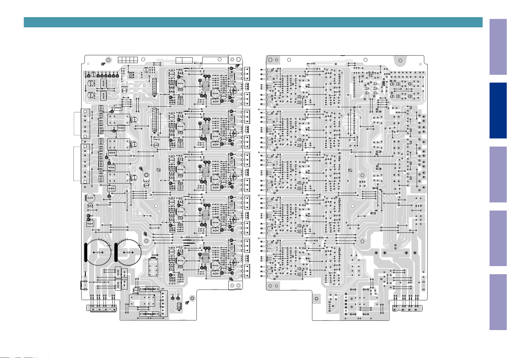
MAIN
Before Servicing
This Unit
MAIN (A SIDE) MAIN (A SIDE)
VERSION
R5505
C5503
J5518
R5405
C5403
J5418
R5305
C5303
J5318
R5205
C5203
J5218
C5206
R5209
R5208
D5201
R5105
J5118
R5727
3.HP_LCH
2.AGND
1.HP_RCH
BN505
J5603
J5501
J5515
J5514
R5522
R5520
J5509J5409J5309J5209
J5513
Q5503Q5403Q5303Q5203Q5103
R5510R5410R5310R5210R5110
FR
R5532
J5512
J5511
R5521
R5519
R5530
R5529
J5510
C5506
R5509
R5508
D5501
C5406
R5409
R5408
D5401
C5305
C5306
R5309
R5308
D5301
C5105 C5205 C5505C5405
C5103
C5106
R5109
R5108
D5101
J5401
J5411
J5301
CEN
J5311
J5201
J5101
J5508J5408J5308
J5416
J5415
J5414
R5422
R5420
J5413
SRSLFL
R5432
J5412
R5421
R5419
R5430
R5429
J5410
J5316
J5315
J5314
R5322
R5320
J5313
R5332R5232R5132
J5312
R5321
R5319
R5330
R5329
J5310
J5216
J5215
J5214
R5222
R5220
J5213
J5212
J5211
R5221
R5219
R5230
R5229
J5210
J5208
J5116
J5115
J5604
J5602
R5122
R5120
J5109
J5114
J5113
J5112
R5121
R5119
J5111
R5130
R5129
J5108
L5501
L5401
L5301
L5201
L5101
BAR CODE
CUP12996Z-1 MP 2018.01.11
R5518
J5505
CN550
ECCCBCBC
BE
Q5504Q5505 Q5506
B EB E
J5504
J5507
R5514
R5531
J5503
J5502
R5511
R5528
D5505
VR550
R5527
R5525
D5504
R5533
R5524
J5506
R5534
D5503
D5506
R5513
D5502
C5508
R5517
R5512
R5515
R5523
R5418
C5509
C5507
R5516
J5405
CN540
2SB1560
Q5404
KTC3114KTC3114
BE
B EB E
J5404
J5407
R5414
R5431
J5403
J5402
R5411
R5428
R5427
R5425
R5424
D5406
C5408
R5423
C5409
R5331
R5328
R5327
R5325
R5324
D5306
C5308
R5323
C5309
Q5405 Q5406
VR540
D5405
D5404
R5433
R5434
J5406
R5413
D5403
D5402
R5417
R5412
R5415
R5318
C5407
R5416
J5305
CN530
2SB1560 2SB1560KTC3114
Q5304
BE
B EB E
B E C
J5304
J5307
R5314
J5303
J5302
R5311
Q5305 Q5306
VR530
D5305
D5304
R5333
R5334
J5306
R5313
D5303
R5317
D5302
R5312
C5307
R5316
B E
R5315
R5218
J5205
R5526 R5426 R5326 R5226 R5126
Q5508
Q5507
Q5408
Q5407 Q5307
CEN
Q5308
Pb
CN520
Q5204
KTC3114
BE
B E
J5204
J5207
R5231
R5214
J5203
R5228
J5202
R5211
Q5205 Q5206
R5227
R5225
R5224
D5206
C5208
R5223
C5209
R5131
R5128
R5127
R5125
R5124
D5106
C5108
R5123
C5109
2SD2390 2SD2390 2SD2390 2SD2390
VR520
D5205
D5204
R5233
J5206
R5234
D5203
R5213
D5202
R5217
R5212
R5215
C5207
R5216
J5105
CN510
2SB1560 2SB1560
E
KTC3114
Q5104
BE
B E E EB B
B EB E
R5118
J5107
R5114
J5104
R5111
J5103
Q5105 Q5106
2SD2390
E C B E BC E BC E BC E C E BC E BC B E BC E BC
D5105
J5102
D5104
VR510
J5106
R5133
D5103
R5134
D5102
R5113
R5112
R5117
R5115
C5107
R5116
Q5208 Q5108
Q5207
FLSLSRFR
Q5107
Q5701
R5728
R5811
R5810
Q5603
Q5601
Q5806
Q5708 Q5705
Q5604
C5806
Q5602
R5813
D5809
D5812
R5816
R5815
D5811
D5810
R5814
R5812
D5808
Q5706 Q5703
Q5704Q5707
C5617
C5616
C5619C5620
C5618
Electrical Mechanical Repair Information Updating
J5624
J5620
J5619
J5618
J5617
J5934
J5626
9.THERMALDET_B
8.THERMALDET_A
7.DC_PROT
6.ASO_DET
5.AMPSIG_DET
4.C/S_RLY
3.FRONT_RLY
2.H/P_RLY
1.HI-B_RLY
13.DGND
12.MUTE_+B
11.RLY_GND
10.+12V
9.FR
8.AGND
7.SR
6.AGND
5.CEN
4.AGND
3.SL
2.AGND
1.FL
BN501
J5623
C5723
J5622
CUP12996Z-1 MAIN PART
J5616
1 2 3 4
F5801
J5804
8
J5805
IN
J5615
J5935
C5716
R5713
R5712
R5711
9
BN502
7 13
J5613
R5403
Pb
J5611
J5610
D5601
8 7 6 5
RY560
1.AC_L
2.NC
3.AC_H
4.CEN
5.AC_H
6.NC
7.AC_L
J5933
R5501
C5501
R5502
R5504
C5502
Q5501
Q5502
R5503
R5506
R5507
C5504
R5401
C5401
R5402
R5404
C5402
Q5401
J5614
Q5402
J5419
R5406
R5407
C5404
J5417
R5301
C5301
R5302
R5304
C5302
Q5301
Q5302
R5303
R5306
R5307
C5304
J5317
J5612
R5201
C5201
R5202
R5204
C5202
Q5201
Q5202
R5203
R5206
R5207
C5204
J5609
J5608J5605
J5607
J5606
R5101
C5101
R5102
R5104
C5102
Q5101
Q5102
R5106
R5107
C5104
R5103
R5726
CN503
FCT1FCT2 RPICTMI
RPICT
C5701
R5702
R5701
R5720
R5719
R5718
R5717
R5716
R5715
R5714
C5717
D5703
C5712C5710
R5707
R5708R5706
C5713C5711
D5704
R5705
C5606
C5608
C5607
C5605
R5722
J5677
JK503
J5656
JK504
J5655
C5706
CMD1A569-V1
J5629
-
FR
FL
J5658
CEN
SR
J5657
SL
C5708
J5645
R5710
J5630
~~
J5662
C5611C5610C5609
C5614C5613C5612
R5725
J5659
R5723
J5648
J5647
R5709
J5633
J5632
J5631
432
1
5
7 1 2 3 4 5 6
Q5702
J5643
R5704
R5703
C5615
J5601
BK501
J5628
D5701
J5627
R5818
R5817
R5819
D5807
J5672 J5671
J5670
C5807
J5908
J5668
J5667
J5666
J5665J5517
C5719
5 4
6
2 3
1
C5718
J5661
J5646
J5644
J5634
J5669
R5721
5 4
2 3
C5722
R5724
J5660
5 4
2 3
J5641
J5640
J5639
J5638
J5637
J5636
C5721
C5720
J5654
J5653
C5714
J5642
C5715
D5701
J5635
RY562
6
1
RY564
J5664J5621
J5663
6
1
RY563
J5652
J5651
J5650
J5649
C5703 C5702
+
J5901
J5902
J5907
J5625
C5601
D5602
J5673
D5604D5603
C5603
ET501
C5602
C5707
C5704
J5904
J5903
C5801
D5806
41
5
J5906
J5905
RY586
F5802
22
Page 23
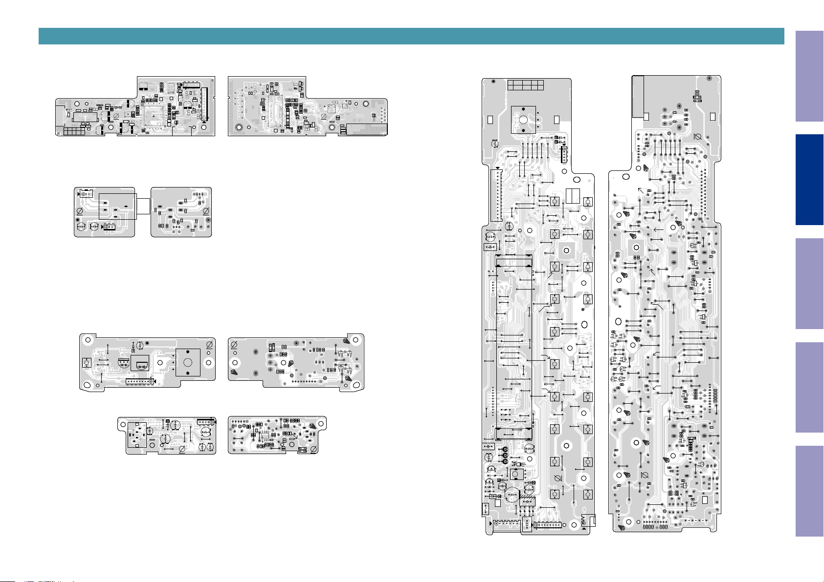
USB, FRONT, PHONE, STANDBY, MIC
5
Before Servicing
This Unit
USB (A SIDE)
C9013
R9065
C9065
R9017
C9049
R9026
R9018
C9009
R9049
C9053
C9078
R9010
R9048
C9098
C9077
R9019
R9020
CUP12965Z
C9023
MP 2018.01.08
C9060
R9073
C9095
C9028
C9076
T9002
L9019
1.VDD
2.RESET
3.RTS
4.CTS
10
5.TXD
6.BT_GND
7.RXD
8.BT_GND
CN911
IC
C9100
C9059
C9033
L9011
D9015
C9030
C9010
T9001
C9019
1 432
9.I2C_SCL
JK91
C9032C9031
10.I2C_SDA
C9125
D9013
D9012
ADJ2ADJ1ICT
RP
L9022
RN909
C9107
C9089
C9088
R9086
T75
C9012
97 128
R9043
R9068
C9086
X9001
R9033
R9069
R9077
R9045
R9071
Pb
C9064
R9066
R9032
C9017
C9087
L9014
C9016
C9011
R9081
IC901
R9092
R9082
C9124
C9014
1.VCC
2.NTRST
PHONE (A SIDE) PHONE (B SIDE)
CN104
LUG13
C1067 C1065
SW101
J1112
1
3287
JK104
BN131
STANDBY (A SIDE)
D1002
BN101
D1012
R W
9
1
C1429
MIC (A SIDE)
JK105
5
3
4
2
6
7
J1111
J1113
J1114
LUG14
C1083
R1057
1.D GND
3.H/P DET
2.D GND
J1106
C1402
J1005
Q1001
F1001
J1004
C1007
C1017
5
8
J1047
J1046
J1045
43
50
53
57
FRONT (A SIDE) FRONT (B SIDE)USB (B SIDE)
LUG11
C1075
BN12B1
1 21
11
27
J1053
C1010
BK101
J1051
FL101
BK102
R1427
C1004
R1426
R1425
Q1014
R1424
R1062
R1007
D1001
1 7
VR101
D1402
D1403
J1102
J1095
J1099
J1098
J1097
J1096
J1094
J1093
J1092
J1090
220 10
J1088
J1089
J1084
J1083
J1082
26
C1019
J1054
J1055
J1052
J1056
J1115
J1050
J1049
J1075
J1057
J1058
J1060
J1048
J1044
J1043
J1041
J1042 J1059
J1040
J1039
J1038
J1037
J1036
J1034
J1033
J1035
J1032
R1067
R1030
J1007
J1006
C1005
J1015
J1008
C1038
J1010
LD101
RC101
D1003
C1003
C1002
J1001
R1002
R1001
CN102
C1001
R1423
J1009
J1064
D1005
C1006
BN12A
J1101
J1100
5
S540BT : ADJUST
SW119
SW113 SW112
SW107
CN103
S640H/S740H : PURE
R1071
S540BT : ADJUST
S640H/S740H : GAME
S640H/S740H : MUSIC
S540BT : BASS/TREBLE
R1082
R1081
S640H/S740H : MOVIE
S540BT : ON/OFF
R1076
R1092
Q1023
Q1022
Q1017
Q1020
R1091
Q1018
/S740H : Q/S_4
R1079
S540BT/S640H/S740H : Q/S_3
R1085
R1080
S540BT/S640H/S740H : Q/S_1
R1075
3.H/P DET
2.D GND
1.D GND
C1081
Q1019
R1090
S540BT/S640H
S540BT/S640H/S740H : Q/S_2
9.POWER_KEY
J1091
SW111
J1087
J1086
J1085
J1078
J1081
J1079
J1077
J1076
SW110
J1067
J1061
J1028
J1062
J1063
J1031
SW116
J1029
J1109
SW109
J1002
R1004
R1003
SW102
J1074
J1080
J1073
J1072
SW118
SW103
J1071
SW114
J1070
J1068
J1066
J1065
SW108
SW117
BN10
J1027
J1026
J1025
SW104
J1020
J1022
J1021
J1023
J1019
J1018
J1024
J1103
J1017
J1014
J1016
J1069
J1013
SW105
J1030
J1012
SW115
J1011
J1003
SW106
BN101_1
1 3
9
3.USB/BT_R
2.DA_GND
5.USB/BT_L
4.DA_GND
C9027
R9062
BN914
R9061
R9063
R9064
R9060
IC906
11 20
10
BN912
5
C9026
C9128
4
L9025
C9070
R9029
RN906
L9029
RN905
T74
65 96
32
3.TDI
4.TCK
L1012
C9111
C9112
IC903
C9113
R9050
R9078
R9042
T62
C9071
R9070
R9040
R9039
C9069
R9041
R9035
R9074
R9036
C9061
C9075
C9074
C9043
R9057
R9034
C9051
C9082
33 64
RN908
RN907
5.TMS
6.TDO
7.RESET
8.DGND
9.DGND
C1424
L1011
L1013
C1069
7 11
85
R9089
IC909
C9109
C9050
C9067
L9027
L9023
C9110
L9026
9
CN913
1.H/P R
L1010
3.H/P L
2.A GND
Pb
C1072 C1071
C1084
C1068
C1066
1.+5VA
C9122
C9120
12.MIC_DET
11.USB_EN
10.USB_DAC_MUTE
9.BX_RST
8.USB_RX
7.USB_TX
6.USB_POWER1(USB1V2)
5.USB3V3
4.DGND
3.DGND
2.D5V
1.D5V
C9021
C9056
IC910
R9024
R9028
C9036
C9054
R9025
C9022
C9035
C9052
BN914-2P
C9020
C9055
28 54
C9121
C9062
C9094
C9063
R9031
R9030
R9058
R9038
R9059
RN904
RN903
C9103
R9093
C9008
C9007
R9055
C9006
R9090
R9054
R9080
R9079
C9093
R9053
C9066
27
C9048
C9090
C9039
C9092
C9091
R9067
R9052
R9044
R9022
R9072
R9056
R9037
R9047
R9088
R9051
C9057
C9038
R9023
RN902
R9046
R9075
R9087
C9047
C9044
R9076
C9079
C9068
C9041
C9080
C9096
C9018
C9042
RN901
C9015
R9085
R9084
R9083
C9046
C9083
C9045
C9084
IC902
C9040
C9099
C9073
L9010
L9015
C9072
C9081
L9018
C9097
C9034
L9013
IC904
4
5 8
IC905
C9037
Pb
R9012
C9029
D9014
D9010
D9011
1.VDD
2.RESET
3.RTS
4.CTS
5.TXD
6.BT_GND
7.RXD
8.BT_GND
9.I2C_SCL
845
10.I2C_SDA
C9058
C9085
L9024
BAR CODE
LABEL
STANDBY (B SIDE)
D1407
D1401
VR102
BN12B
C1405
J1108
J1107
C1407
J1110
C1411
Pb
L1403
C1452
J1104
C1410
R1411
R1412
+12V
-12V
5.MIC DET
4.+12V
3.-12V
2.MIC SIGNAL
1.AGND
D1406
C1428
A
C1426
C B
R1416
C1425
+12V
1.+3v3
6.GRN_LED
7.RED_LED
8.MCU+5
9.POWER_KEY
5.DGND
2.ISEL_A
3.ISEL_B
4.DGND
MIC (B SIDE)
R1408
C1408
R1409
C1417
R1433
R1435
R1434
R1436
C1450
R1405
IC101
5 8
C1413
R1407
C1414
R1027
C1406
4
C1415
C1416
R1431
R1432
R1437
C1451
C1427
R1415
R1413
R1403
R1414
R1042
R1041
R1045
C1055
Q1009
Q1008
Q1012
C1054
R1043
R1044
Q1011
+5V
L1402
L1401
R1401
R1054
C1401
R1402
R1404
R1406
C1404
C1403
D1404
D1405
Pb
BAR CODE
S540BT/S640H/S740H : ADJUST
X250BT/X550BT/X1500H : Q/S_4
R1084
R1087
R1086
Q1024
Q1021
GNDGND
GNDGND
GNDGND
3.ISEL_B
2.ISEL_A
5.DGND
4.DGND
8.MCU+5
7.RED_LED
6.GRN_LED
C1091
C1090
C1089
C1088
1.A GND
2.MIC SIGNAL
3.-12V
4.+12V
5.MIC DET
+12V
R1078
R1083
R1072
R1077
R1073
Pb
R1074
1.+3v3
C1409
R1410
CUP12957Z-1/FRONT PART/MP STAGE
GNDGND
C1076
C1077
-12V
C1082
R1046
X250BT/X550BT/X1500H : Q/S_3
S540BT/S640H/S740H : DIMMER
Cushion
X250BT/X550BT/X1500H : Q/S_2
S540BT/S640H : SLEEP
S740H : MODE
S540BT : MODE
S640H : INFO
S740H : BAND
X250BT/X550BT/X1500H : Q/S_1
S540BT/S740H : TUNE+
X250BT/X550BT/X1500H : STATUS
S640H : MODE
X250BT/X550BT/X1500H : DIMMER
S540BT/S740H : TUNE-
S640H : BAND
X250BT/X550BT/S640H : TUNE+
S540BT/S740H : PRESET+
X1500H : ZONE2 SEL
S540BT/S740H : PRESET-
X250BT/X550BT/S640H : TUNE-
X1500H : ZONE2 ON/OFF
R1022
S640H/X1500H : PRESET+
X250BT/X550BT : PRESET+
S740H : ZONE2 SEL
S540BT : SOUND
R1024
C1039
S640H/X1500H : PRESET-
S740H : ZONE2 ON/OFF
X250BT/X550BT : PRESET-
S540BT : SOUND
R1008
R1005
+3.3V
C1087
C1086
C1085
GND
R1068
R1023
R1011
R1010
Q1002
R1053
R1418
Q1016
R1421
R1420
R1419
R1009
R1006
R1020
R1021
R1069
C1073
C1074
GNDGND
R1017
R1019
C1009
Q1007
R1430
D1015
D1016
Q1006
R1015
R1014
R1013
Q1005
R1058
R1059
-12V
R1026
R1061
R1060
R1012
R1429
L1001
R1428
+3V3
C1020
Q1003
D1408
C1430
7.FL AC
Pb
R1422
Q1004
GNDGND
Q1015
Q1013
6.NC
R1025
5.FL AC
1.ISEL_A
2.ISEL_B
3.MIC_DET
4.POWER_KEY
5. +12V
6. -12V
7.MIC_SIGNAL
8.A_GND
9.B/P_IRIN_DE
10.H/P_DET
11.VSEL_A
12.VSEL_B
13.KEY_3
14.KEY_2
15.KEY_1
16.RED_LED
17.GRN_LED
18.RC_IN
19.FL_RST
20.FL_CE
21.FL_CLK
22.FL_DATA
23.CPU_POWER
24.MCU_5V
25.MCU_3V3
26.D_GND
27.NET_FACT_RST
+12V
Electrical Mechanical Repair Information Updating
C1011
C1041
R1018
R1016
C1013
C1014
C1015
C1016
C1012
C1423
2.NC
3.GND
4.NC
1.VDISP
23
Page 24
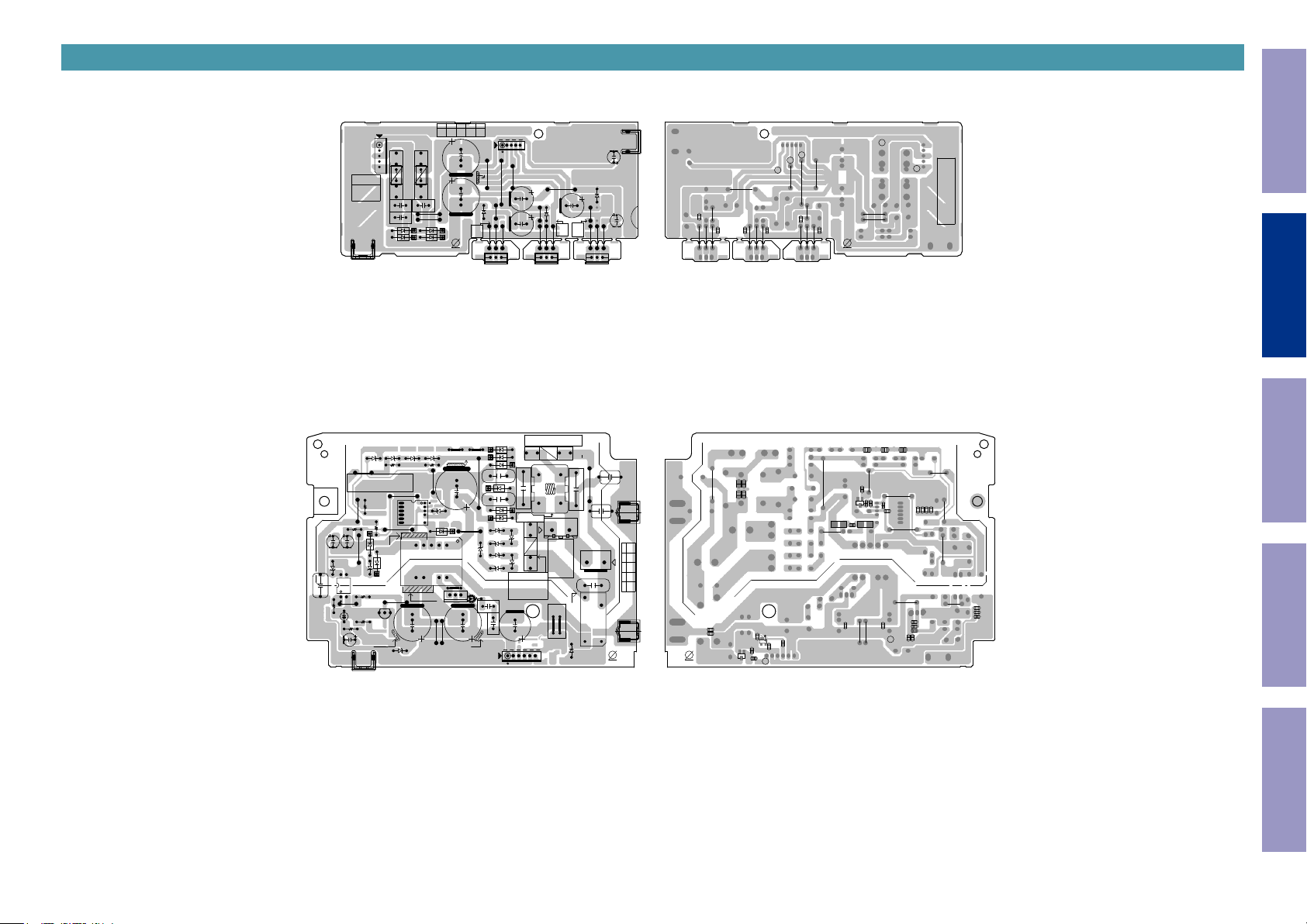
REGULATOR, SMPS
BOTTOM SIDE BOTTOM SIDE BOTTOM SIDE
Before Servicing
This Unit
CUP12910Z-1
SMPS PART
MP_STAGE
Sec.
Pri.
C6008 C6013
ZD620
C6023
R6017
R6021
C6010
BK303
BK603
1.AC_S2
2.NC
3.RTN_GND
4.NC
5.AC_S2
1A387
R6015
IC602
D6010
1A629
AC120V
F3003/F3004
AC100V
AC220~230V
F3001/F3002
J6004
BAR CODE
J6007
D6007
J6009
ZD618
Pri.
R6016
J6013
R6018
1 5
ZD621
R6004
R6010
D6008
Sec.
IC603
BONDING
REGULATOR (A SIDE)
CUP12910Z-2
REGULATOR PART
MP_STAGE
CN302
T 1.25A L 250V
T 1.25A L 250V
T 1.25A L 250V
T 1.25A L 250V
F3003
F3004
F3002
F3001
C3003
C3005
C3004
J3004
J3006
D3003
D3001
D3004
D3002
SMPS (A SIDE) SMPS (A SIDE)
ZD609
ZD608
ZD610
R6009 R6008
J6016
J6017
V
12 7
S
S
X
C
S
F
S
ZD601
S
6
D
S
D6012
J6018
IC601
BONDING
T6001
D6013
J6012
BONDING
R A C
J6020
J6019
C6019
ZD619
FCT1 FCT2 RPICTMI
C3007
Pb
BONDING
C6004
1 7
14 8
C6018
BONDING
REGULATOR (B SIDE)
5.DA+5V
4.VGND
3.+12V
2.RLY_GND
DA+5V TP
+12V TP
1.-12V
-12V TP
AC_S2 TP
AC_S2 TP
1.AC_S2
2.NC
3.RTN_GND
4.NC
5.AC_S2
BAR CODE
C3011
C3014
C6029
C6030
IC604
C3015
Pb
R6033R6032R6031
R6006
R6013
R6014
V
Q6002
X
C
F
C6026
C6011
R6011
D
Pri.
Sec.
C6015
C6014
L6001
C6012
D5.2V TP
C6009
C6007
C6006
C6005
S
S
R6012
S
S
S
S
R6022
R6023
C6020
R6020
R6019
Sec.
Pri.
Pri.
Sec.
C6024
C6025
R6026
Electrical Mechanical Repair Information Updating
BK301
J3015
C3008
1 .IN
1 .IN
2 .GND
3 .+12V
2 .GND
3 .+5VV
IC301
F6001
CX601
J6011
LF602
CN602
CN601
T 6.3A L 250V
(AC100V~120V AREA)
(AC220V~230V AREA)
C6001
J6015
BONDING
4 3
RY601
D6009
1A569-V1
C3024
D3101
D3108
J3013
C3001
J3032
J3033
J3034
I OG I G O OG I
IC305
KIA7805BPI
CY602
BK601
1A834
CY601
LN
FCT1 FCT2 RPICTMI
Pri.
2
Sec.
BK602
1A834
1
Pb
C3002
L N
Pri.
Sec.
C6022
C6021
Pb
C3009
C3010
R6027
R6029
R6030
R6028
R6024
Q6003
R6025
MAIN_POWER TP
5.DA+5V
3.+12V
1.-12V
2.RLY_GND
4.VGND
C3006
2 .IN
3 .-12V
J6003J6002
J6005
D6004
D6002
J6010
ZD617
Pri.
Sec.
J6001
R6034
1.D5.2V
2.D5.2V
BONDING
1 .GND
D6005
C6003
4.D_GND
3.M_RESET
D3104
J3026
C6028
5.D_GND
6.MAIN POWER
J3023
C3012
J3035
C3013
J3028
J3027
ZD611
ZD613
ZD614
ZD616
C6027
BN601
BN301
5
J3025
J3024
J3036
D3103
J3031
J3030
J3037
KIA7912 KIA7812
IC302
(AC220V~240V AREA)
T1.6A L 250V
T2A L 250V
(AC100V~120V AREA)
D6006
D6001
D6003
C6002
3
CX602
LF602
CLZ9Z126Z:E3,K
CLZ9Z133Z:E2,E1C
ZD612
ZD615
F6002
AVR-S730H/X1400H
AVR-S530BT/X540BT
T 2.5A L 250V
(AC220V~230V AREA)
T 5A L 250V
(AC100V~120V AREA)
C6017
OPEN
OPEN
6
142
T 3.15A L 250V
J6014
24
Page 25
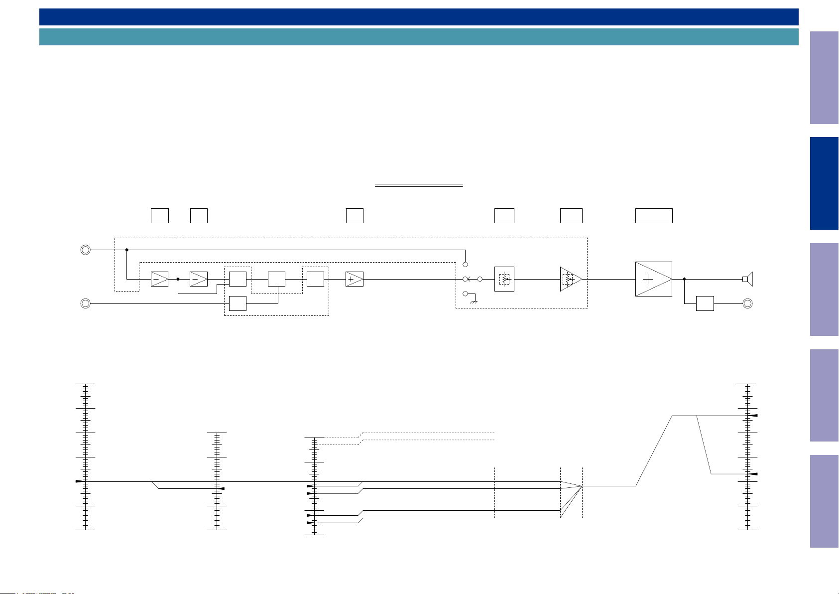
LEVEL DIAGRAM
FRONT ch
Before Servicing
This Unit
AVRS540BT /X550BT/X250BT L EVEL1 DIAG RAM
AUDIO IN
DIG ITAL
40dB
30dB
20dB
10dB
2CH IN 0dB
(200m V)
-10dB
-20dB
FR O NT
-2. 78dB
A/D IN
REV A MP
A/D IN
REV AM P
CS 42528
DIFF. INPUT
0dBFS= 5.6V pp
AD IN=145m V
A/ D
=1 .98Vrm s
A/ D
DIR
0dBF S
-10dBF S
-20dBFS
-22.78dB FS
(A/ D IN )
-30dBFS
-40dBF S
DS P
CS 42528
0dBF S
-10dBF S
-20dBF S(D IG.IN )
-22.78dB FS
(A/ D IN )
-30dBFS
-32dBF S(D IG.IN )
-34.78dBFS
(A/ D IN )
-40dBF S
D/ A
D/ A
CS 42528
DIFF. OUT
0dBF S=5V pp
=1 .77Vrm s
FRO NT ch
D/A OU T
LPF
FU LL SCA LE L EVEL =2V rms
DO LBY LIM IT LEVEL (ALL ch-3dBFS )
+1 .77dB
+1 .77dB
+1 .77dB
+1 .77dB
ELE CTRIC
VO LUM E
NJ U72340A FH 3
VO L 0 0
PRE AM P1
-2dB
+1dB
+10dB
+13dB
GA IN s etting of MASTER VOL 00dB
-SW :YES(D IGIT AL)
-SW :YES(A NAL OG)
-SW :N ONE (DIG ITAL)
-SW :N ONE (ANA LOG)
=- 2dB
=+1dB
=+10dB
=+13dB
+29dB
PO WER AM P
-24dB
AT T
40dB
30dB
20dB
10dB
-10dB
-20dB
0dB
SPK O UT
FR ONT
H/P OU T
SPK O UT
FR ONT
4.47V rms /8ohm
H/P OU T
282mV rms
/33ohm
Electrical Mechanical Repair Information Updating
25
Page 26
CENTER ch
Before Servicing
This Unit
AVRS540BT /X550BT/X250BT L EVEL2 DIAG RAM
40dB
30dB
20dB
10dB
2CH IN 0dB
(200m V)
-10dB
-20dB
CE NT ER
DSP OUT
-20dBF S(D IG.IN )
-22.78dB FS
0dBF S
-10dBF S
(A/ D IN )
-30dBFS
-40dBF S
D/ A
D/ A
CS 42528
DIFF. OUT
0dBF S=5V pp
=1 .77Vrm s
CENTER ch
D/A OU T
LPF
FU LL SCA LE L EVEL =2V rms
DO LBY LIM IT LEVEL (ALL ch-3dBFS )
+1 .77dB
+1 .77dB
ELE CTRIC
VO LUM E
NJ U72340A FH 3
VO L 0 0
PRE AM P1
+29dB
-2dB
+1dB
GA IN s etting of MASTER VOL 00dB
-PC M or DD C onfig1(D IG.IN )
-A/ D IN (ANA LOG)
-DD C onfig2(D IG.IN )
=- 2dB
=+1dB
=+1dB
PO WER AM P
40dB
30dB
20dB
10dB
-10dB
-20dB
0dB
SPK O UT
CE NTER
SPK O UT
FR ONT
4.47V rms /8ohm
Electrical Mechanical Repair Information Updating
26
Page 27

SURROUND ch
Before Servicing
This Unit
AVRS540BT /X550BT/X250BT L EVEL3 DIAG RAM
40dB
30dB
20dB
10dB
2CH IN 0dB
(200m V)
-10dB
-20dB
SURRO UND
DSP OUT
-20dBF S(D IG.IN )
-22.78dB FS
0dBF S
-10dBF S
(A/ D IN )
-30dBFS
-40dBF S
D/ A
D/ A
CS 42528
DIFF. OUT
0dBF S=5V pp
=1 .77Vrm s
SURRO UND ch
D/A OU T
LPF
FU LL SCA LE L EVEL =2V rms
DO LBY LIM IT LEVEL (ALL ch-3dBFS )
+1 .77dB
+1 .77dB
ELE CTRIC
VO LUM E
NJ U72340A FH 3
VO L 0 0
PRE AM P1
+29dB
-2dB
+1dB
GA IN s etting of MASTER VOL 00dB
-PC M or DD C onfig1(D IG.IN )
-A/ D IN (ANA LOG)
-DD C onfig2(D IG.IN )
=- 2dB
=+1dB
=+1dB
PO WER AM P
40dB
30dB
20dB
10dB
-10dB
-20dB
0dB
SPK O UT
SURRO UND
SPK O UT
FR ONT
4.47V rms /8ohm
Electrical Mechanical Repair Information Updating
27
Page 28

SUBWOOFER ch
Before Servicing
This Unit
AVRS540BT /X550BT/X250BT LEVEL4 DIAG R AM
40dB
30dB
20dB
10dB
2CH IN 0dB
(200m V)
-10dB
-20dB
SU BW OOFER
DSP O UT
-30dBFS( DIG .IN)
DD Conf ig1
-37dBF S(A /D IN )
0dBF S
-10dBF S
-20dBF S
-40dBF S
D/ A
D/ A
CS 42528
DIFF. OUT
0dBF S=5V pp
=1 .77Vrm s
SUBW OOFER ch
D/A OU T
LPF
REV AM P
FU LL SCA LE L EVEL =2V rms
DO LBY LIM IT LEVEL (ALL ch-3dBFS )
+8 .2dB
+8 .2dB
SW SUM
REV AM P
ELE CTRIC
VO LUM E
PRE AM P1
NJ U72340A FH 3
+12dB
VO L 0 0
+15dB
M UT E
40dB
30dB
20dB
10dB
0dB
-10dB
-20dB
SW W OOFER
PR EOU T
PR EOU T
SU BWOOF ER
500mV rms
PR EOU T
SU BWOOF ER
316mV rms
Electrical Mechanical Repair Information Updating
28
Page 29

BLOCK DIAGRAM
ANALOG AUDIO DIAGRAM
AVR-S540BT/X550BT/X250BT ANALOG AUDIO BLOCK
AUDIO IN
MEDIA PLAYER
CBL/SAT
SETUP MIC
MIC'
*AVR-S540BT/X550BT: USED
TUNER
TUNER
FM/AM
V+:+7.5V
V-:-7.5V
* LOGIC CONTROL HIGH LEVEL INPUT VOLTAGE(MIN: +2.5V / MAX: V+)
MAIN
ANA_FL
ANA_FR
DA_CEN
DA_SW
DA_SL
DA_SR
DA_SBL
DA_FL
DA_FR
MAIN AMP
2SD2390/2SB1560
H/P OUT
SPK OUT
+
-
+
-
+
-
+
-
+
-
H/P L
GND
H/P R
FL
FR
CEN
SL
SR
Before Servicing
This Unit
Electrical Mechanical Repair Information Updating
AD_FL
AD_FR
USB/BT_IN(AVR-S540BT/X550BT)
BT_IN(AVR-X250BT)
DA_FL
DA_FR
TO DIGITAL
DA_CEN
AUDIO BLOCK
DA_SW
DA_SL
DA_SR
29
DA_SBR
VOL IC
NJU72340A
PRE OUT
MUTE
AVR-X250BT: USED SW1
AVR-S540BT/X550BT: USED SW1 & SW2
SW1
SW2
Page 30

DIGITAL AUDIO / HDMI DIAGRAM
AVR-S540BT/X550BT/X250BT DIGITAL AUDIO/HDMI BLOCK
DIGTAL IN
OPTICAL IN1
OPTICAL IN2
COAXIAL IN1
DIR IN OPTION
OPT IN
COAX IN
2
2
2
VDD:USB3V3
IPOD AUTH.
I2C
USB
DECORDER
(BX8804)
MCU
VDD:MCU+3V3
1
0
0
AUDIO DAC
I2S
(PCM5100A)
CPVDD: 3V3
DVDD: 3V3
S.FLASH
32M
For GUI
VCC:CEC3V3
HDMI RX
ADV7623
CVDD, DVDD:D1V8H
PVDD:D1V8H
TXAVDD:D1V8H
TXPVDD:D1V8H
TXPLVDD:D1V8H
DVDDIO:CEC3V3
TVDD:CEC3V3
S540BT
X550BT
X250BT
VDD:USB3V3
BT
MODULE
USB IN
USB
*AVR-S540BT/X550BT:USED
BT
MODULE
*AVR-X250BT:USED
VDD:USB3V3
HDMI IN1
HDMI IN2
HDMI IN3
HDMI IN4
HDMI IN5
UART
D+/-
UART
TMDS
TMDS
TMDS
TMDS
TMDS
23671011050AS
(MFI337S3959)
VDD33:USB3V3
VDD12:USB1V2
I2S
TMDS
S.FLASH
32M
For GUI
VCC:CEC3V3
VDD11: CEC1V1
VDD33:CEC3V3
AVDD11:CEC1V1
AVDD33:CEC3V3
AVDDH33:CEC3V3
PVDD33:CEC3V3
HDMI TX(4K)
MN864788
Before Servicing
This Unit
DIR/CODEC
VD:+3V3D
VD:+5VD
LRCK
SCLK
SD0
SD1
SD2
CODEC
SD3
SERIAL
PORT
+
ADC
-
+
ADC
-
INPUT
SELECT
SN74AHC157PWR
HDMI MCLK
MCLK
SPDIF/SDATA3 (FOR ARC)
HDMI_SDATA0
HDMI_SDATA1
HDMI_SDATA2
HDMI_SDATA3
HDMI_LRCLK
HDMI_SCLK
HDMI_MCLK
TMDS
TX0
TMDS
TX1
DIGITAL
FILTER
DIGITAL
FILTER
MUX
VCC:+3V3D
+3V3D
VOLUME
CONTROL
Rx
CS42528
GAIN
&
CLIP
GAIN
&
CLIP
CLK/DATA
RECOVERY
DIGITAL
FILTER
SERIAL
RMCK
LRCK
SCLK
SD0
SD1
SD2
SD3
ADC
DATA
DAC
DAC
DAC
DAC
ANALOG
DAC
FILTER
DAC
DAC
DAC
+3
SERIAL
AUDIO I/F
DEM
S/PDIF
DECODER
OMCK
VDD:+1V8H
VDDA:+3V3D
DAO_MCK
VDDIO:+3V3D
XOUT
V3D
SAI_SCLK
SAI_LRCK
SAI_SDO
DSP
CS497024
S.FLASH
8M
VCC:+3V3D
SDRAM
16M
VCC:+3V3D
DA_FL
DA_FR
DA_CEN
DA_SW
DA_SL
DA_SR
Electrical Mechanical Repair Information Updating
--
AD_FL
--
AD_FR
DA_FL
DA_FR
DA_CEN
DA_SW
DA_SL
DA_SR
USB/BT_IN
HDMI OUT
TO ANALOG
AUDIO BLOCK
30
Page 31

VIDEO DIAGRAM
HDMI IN
HDMI IN1
(DVD/Blu-ray)
HDMI IN2
(MEDIA PLAYER)
RXA
RXB
RXC
AVR-S540BT/X550BT/X250BT VIDEO BLOCK
ADV7623
TRANSCEIVER
OSD Block
CVDD, DVDD:D1V8H
PVDD:D1V8H
TXAVDD:D1V8H
TXPVDD:D1V8H
X7201
28.6363MHz
TXPLVDD:D1V8H
DVDDIO:CEC3V3
TVDD:CEC3V3
S.FLASH
32M
For GUI
VCC:CEC3V3
Before Servicing
This Unit
Electrical Mechanical Repair Information Updating
HDMI IN
HDMI IN3
(CBL/SAT)
HDMI IN4
(Blu-ray)
HDMI IN5
(GAME)
CVBS IN
MEDIA PLAYER
CBL/SAT
P2 RX
P1 RX
P0 RX
NJM2595
P3 RX
MAIN
P2 RX
P1 RX
SUB
P0 RX
S.FLASH
32M
For GUI
VCC:CEC3V3
V+:+5V
V-:-5V
75ohm
6dB
20K
20K
20K
20K
Driver
75ohm
6dB
Driver
75ohm
6dB
Driver
27.000MHz
P0 TX
P1 TX
VDD11: CEC1V1
VDD33:CEC3V3
AVDD11:CEC1V1
AVDD33:CEC3V3
AVDDH33:CEC3V3
PVDD33:CEC3V3
HDMI OUT
MONITOR OUT
CVBS OUT
MONITOR OUT
HDMI TX(MN864788)
31
Page 32

POWER DIAGRAM
!
AVR-S540BT/X550BT/X250BT VCC DIAGRAM
!
S1(AMP+B,-B)
S2(+12V,-12V)
MAIN TRANS
HI+B
LOW+B
HI-B
LOW-B
2
4
1
3
TFZV7.5B
KIA7805BPI
KIA7812BPI
KIA7912PI
TFZV7.5B
MM1Z525V1B
MM1Z525V1B
37mA(28mA)
BU33TD3WG
178mA
10mA
50mA
75mA
25mA
22mA
25mA
45mA
MAIN+B
MAIN-B
RELAY*5
VOLUME IC
(NJU72340A)
A+12V
(NJM8080 X 4)
DA+3.3V
+5VA
(NJM2740V X 2)
TUNER+5V
CS42528(VA)
A-12V
VOLUME IC
(NJU72340A)
V+5V
(NJM2595)
V-5V
(NJM2595)
(USB DAC:PCM5100A)
Before Servicing
This Unit
Electrical Mechanical Repair Information Updating
S2 TOTAL : 415.6mA(AVR-S540BT/X550BT)
S2 TOTAL : 406.6mA(AVR-X250BT)
AC CORD
RELAY
!
S4(FL+Vdisp)
!
68mA
163mA
Vdisp(+37V)
FILAMENT AC
S5(FILAMENT)
FILAMENT AC
1
2
*DC-DC Effieciency:85%
+5.2V
MAIN PWR ON
(5.2V)
(5.2V)
(5.2V)
(5.2V)
TPS563200I(+3.3V)
BU12TD3WG
TPS563200(+1.8V)
TPS563200R(+1.1V)
AP7361-Y-13
(5.2V)
1281.91mA(AVR-S540BT/X550BT)
844.02mA(AVR-X250BT)
60mA
589.95mA
291.92mA
158.02mA
OPEN
650mA(50mA)
0.005mA
20mA
113mA
1000mA
20mA
357.5mA
410mA
339mA
60mA
982mA
500mA
1200mA
158mA
0.02mA
(HDMI CEC CONTROL/SN74CBT3251PWR)
SWM5V
FRONT LED(CVDBLBJEGJ204L)
MCU+5V
CS42528(VD), OPTICAL JACK X 2
D5V/VBUS : Only AVR-S540BT/X550BT USED
CEC5V/HDMI & DSP
+3V3D/DIR,DSP
(CS497024,CS42528,M12L16161A5TG2Q,EN25Q80B104HIP,SN74AHC157PWR)
CEC3V3/HDMI
(MN864788,EN25QH32B104HIP2B)
DV3.3V/ADV7623,EN25QH32B104HIP2B
USB3V3/BX8804,W9864G6JH-6, EN25QH16B104HIP2A, BT MODULE, IPOD CP : (Only AVR-S540BT/X540BT)
(USB3V3/BT MODULE: Only AVR-X250BT)
USB1V2/USB(Only AVR-S540BT/X550BT USED)
(BX8804)
D1V8H/HDMI
(ADV7623)
+1V8/DSP
(CS497024)
CEC1V1/HDMI TX
(MN864788)
MCU_3V3/MICOM
(STM32F101ZG,M24C32WMN6TP,PST8425NR,VFD)
SWM3V3/DETECT PULLUP
* TOTAL (5V): 1153.005mA(AVR-S540BT/X550BT)
* TOTAL (5V): 153.005mA(AVR-X250BT)
INPUT CURRENT (Ref Volage:5.2V)
SMPS Total Current : About 3607.786mA(AVR-S540BT/X550BT)
SMPS Total Current : About 2109.901mA(AVR-X250BT)
D
S
4
G
3
32
Page 33

WIRING DIAGRAM
AVR-S540BT/X550BT/X250BT WIRING DIAGRAM
AC CORD
BN601
6P
SMPS PCB
SMPS<-AC IN
CN602
2P
CN601
2P
TRANS -> SMPS
5P
5P
REGULATOR PCB
CN302
SMPS<-DIGITAL
BN301
REGUL.<- DIGITAL
CN771
5P
CN751
6P
DIGITAL PCB
CN711
27P
CN741
Before Servicing
This Unit
CN781
VIDEO & D_AUDIO PCB
9P
9P
CN752
CN772
13P
CN712
9P
CN713
11P
5P
Electrical Mechanical Repair Information Updating
TRANS
TRANS -> FRONT
BN101_1
9P
POWER LED<->FRONT
9P
BN101
FUNCTION
ENCODER
POWER
LED PCB
CN102
7P
TRANS -> REGUL.
TRANS->MAIN
CN104
H/P PCB
BN501
MAIN->DIGITAL
13P
7P
CN503
BN505
3P
FRONT <-> DIGITAL
27P
BN12B1
H/P <- MAIN
CN103
3P
3P
3P
BN131
FRONT PCB
BN12A
5P
H/P-FRONT
MIC PCB
BN12B
MIC
5P
BT MODULE
10P
CN911
USB
10P
USB & BT PCB
*AVR-S540BT/X550BT:MIC & USB & BT USED
USB & BT <-> DIGITAL
5P
BN914
11P
BN912
* AVR-X250BT: ONLY BT USED
MAIN PCB
USB & BT <-> DIGITAL
11P
BN912
5P
BN911
BT PCB
BT MODULE
BN502
MAIN->DIGITAL
9P
33
Page 34

PC13-TAMPER-RTC
SEMICONDUCTORS
Only major semiconductors are shown, general semiconductors etc. are omitted to list.
The semiconductor which described a detailed drawing in a schematic diagram are omitted to list.
1. IC's
STM32F101ZE (DIGITAL : IC711)
DD_3VSS_3
V
144
PE2
1
PE3
2
PE4
3
PE5
4
PE6
5
VBAT
6
V
SS_5
V
DD_5
PF10
OSC_IN
OSC_OUT
NRST
V
SSA
V
REF-
V
REF+
V
DDA
PA0-WKUP
7
8
9
PF0
10
PF1
11
PF2
12
PF3
13
PF4
14
PF5
15
16
17
PF6
18
PF7
19
PF8
20
PF9
21
22
23
24
25
26
PC0
27
PC1
28
PC2
29
PC3
30
31
32
33
34
35
PA1
36
PA2
3738394041424344454647484950515253545556575859
PA3
PC14-OSC32_IN
PC15-OSC32_OUT
STM32F101ZG Terminal Functions
Pin Pin Name Symbol
1 PE2 DC_PROTECT
2 PE3 USB_DAC_MUTE
3 PE4 POWER_DOWN
4 PE5 FRONT_RLY(SPK_RLY_ON)
5 PE6 C/S_RLY
6 VBAT VBAT
7 PC13 MIC_DET
8 PC14 / OSC32_IN OSC32_IN
PC15 / OSC32_
9
OUT
10 PF0 ISEL_B
11 PF1 ISEL_A
12 PF2 HI-B_RLY
13 PF3 CVBS_SW2
14 PF4 CVBS_SW5
15 PF5 CP_SDA
16 VSS_5
17 VDD_5
18 PF6 CEC_POWER2
19 PF7 USB_EN
20 PF8 HPD3
OSC32_OUT
PE1
PE0
PB9
PB8
BOOT0
143
142
141
140
139
138
PA4
PA5
PA6
PA7
SS_4
DD_4
V
V
DD_11VSS_11
PB7
PB6
PB5
PB4
PB3
PG15
V
PG14
137
136
135
134
133
132
131
130
129
LQFP144
PB0
PB1
PB2
PC4
PC5
PF11
PF12
DD_6
VSS_6
V
I/O Pullup STBY
PG13
128
PF13
PG12
127
PF14
PG11
PG10
126
125
PG0
PF15
Pass-
Trough
PG9
124
PG1
DD_10VSS_10
PD7
PD6
V
PD5
PD4
123
122
121
120
119
118
60
6162636465666768697071
PE7
PE8
PE9
PE10
SS_7
DD_7
V
V
BT
STBY
I M3VPu I I I I
O - O/L O/L O/L O/L
I M3VPu I I I I
O - O/L O/L O/L O/L
O - O/L O/L O/L O/L
- - - - - -
I Pd I I I I
- - - - - -
- - - - 0 -
I Pu I I I I
I Pu I I I I
O - O/L O/L O/L O/L
O - O/L O/L O/L O/L
O - O/L O/L O/L O/L
O - O/L O/L O/L O/L
- - - - - -
- - - - - -
O - L H L O/L
O - O/L O/L O/L O/L
O - O/L O/L O/L O/L
PD3
PD2
PD1
PD0
PC12
PC11
PC10
PA15
PA14
117
PE11
stop
116
PE12
109
115
114
113
112
111
110
108
V
DD_2
107
V
SS_2
106
NC
105
PA13
104
PA12
103
PA11
102
PA10
101
PA9
100
PA8
99
PC9
98
PC8
97
PC7
96
PC6
95
V
DD_9
94
V
SS_9
93
PG8
92
PG7
91
PG6
90
PG5
89
PG4
88
PG3
87
PG2
86
PD15
85
PD14
84
V
DD_8
83
V
SS_8
82
PD13
81
PD12
80
PD11
79
PD10
78
PD9
77
PD8
76
PB15
75
PB14
74
PB13
73
PB12
72
PE13
PE14
PE15
PB10
PB11
SS_1
DD_1
V
V
Function
DC Protection Detect
USB_DAC_MUTE control
Power Down detect
Front SPK RLY control
Surround/Center SPK RLY control
3.3V
MIC detect
FUNCTION ENDORDER input(A)
FUNCTION ENDORDER input(B)
HI-B_RLY control
CVBS(Video)SW2 control
CVBS(Video)SW5 control
APPLE AUTH CHIP_I2C_SDA (for AVR-
X250BT option)
GND
3.3V
CEC_POWER2 control
USB_CURRENT IC control
HDMI INPUT3 HOT PLUG control
Pin Pin Name Symbol
21 PF9 MAIN_VOL_DATA
22 PF10 MAIN_VOL_CLK
23 PH0 / OSC_IN XTAL_IN
24 PH1 / OSC_OUT XTAL_OUT
25 NRST RESET
26 PC0 KEY1
27 PC1 KEY2
28 PC2 KEY3
29 PC3 OPTION
30 VSSA
31 VREF32 VREF+
33 VDDA
34 PA0 / WKUP CP_SCL
35 PA1 USB_RESET
36 PA2 USB_RX
37 PA3 USB_TX
38 VSS_4
39 VDD_4
40 PA4 DSP_CS
41 PA5 DSP_CLK
42 PA6 DSP_MISO
43 PA7 DSP_MOSI
44 PC4 HPD4
45 PC5 HPD5
46 PB0 DIR_MISO
47 PB1 DIR_CLK
48 PB2 / BOOT1 BOOT1
49 PF11 DIR_MOSI
50 PF12 DSP_RST
51 VSS_6
52 VDD_6
53 PF13 DSP_MODE_SEL
54 PF14 CODEC_MUTE
55 PF15 DIR_RST
56 PG0 DIR_CE
57 PG1 DSP_SPC1_IRQ
58 PE7 DSP_PCP_BSY
59 PE8 CEC_POWER
60 PE9 HDMI_SW
61 VSS_7
62 VDD_7
63 PE10 DV5_POWER
64 PE11 HDMI_SPI_MISO
65 PE12 HDMI_SPI_MOSI
66 PE13 HDMI_SPI_CS
67 PE14 HDMI_SPI_CLK
68 PE15 HDMI_SPI_HOLD
Pass-
I/O Pullup STBY
Trough
BT
STBY
stop
O - O/L O/L O/L O/L
O - O/L O/L O/L O/L
I - - - - -
O - - - - -
I - - - - -
I M3VPu I I I I
I M3VPu I I I I
I M3VPu I I I I
I M3VPu I I I I
- - - - - -
- - - - - -
- - - - - -
- - - - - -
O - O/L O/L O/L O/L
O - O/L O/L O/L O/L
USB-
O
I
O/L O/L O/L O/L
3V3Pu
USB-
I I I I
3V3Pu
- - - - - -
- - - - - -
O - O/L O/L O/L O/L
O D3VPu O/L O/L O/L O/L
I D3VPu I I I I
O - O/L O/L O/L O/L
O - O/L O/L O/L O/L
O - O/L O/L O/L O/L
I - I I I I
O - O/L O/L O/L O/L
I - - - - -
O - O/L O/L O/L O/L
O - O/L O/L O/L O/L
- - - - - -
- - - - - Pull-
I/O
O/L O/L O/L O/L
Down
I(FT) - O/L O/L O/L O/L
O - O/L O/L O/L O/L
O - O/L O/L O/L O/L
I D3VPu I I I I
I D3VPu I I I I
O - L H L O/L
O - O/L O/L O/L O/L
- - - - - -
- - - - - -
O - O/L H H O/L
I - I I I I
O - O/L O/L O/L O/L
O +3VHPu O/L O/L O/L O/L
O - O/L O/L O/L O/L
O - O/L O/L O/L O/L
Function
Volume Data
Volume CLK
XTAL_IN(8MHz)
XTAL_OUT(8MHz)
RESET
KEY1
KEY2
KEY3
MODEL OPTION
GND
GND
3.3V
3.3V
APPLE AUTH CHIP_I2C_SCL (for AVR-
X250BT option)
BX8804(USB DECORDER) RESET
BX8804(USB DECORDER) RX
BX8804(USB DECORDER) TX
GND
3.3V
DSP Chip Select
DSP_CLK
DSP MISO
DSP MOSI
HDMI INPUT4 HOT PLUG control
HDMI INPUT5 HOT PLUG control
DIR_MISO
DIR_CLK(separated from AVR1312 DSP_
CLK)
GND
DIR MOSI(separated from AVR1312 DSP_
MOSI)
DSP Reset control
GND
3.3V
DSP_MODE_SEL
CODEC Mute Detect (*FT = 5V tolerant)
DIR Reset
DIR Chip Select
DSP INTERRRUPTQ
DSP BSY
CEC_POWER TIMING control
HDMI Audio Data MCLK Select SW
GND
3.3V
DV5_POWER TIMING control
HDMI OSD DATA input
HDMI OSD DATA output
HDMI OSD Chip Select
HDMI OSD Clock
HDMI OSD HOLD
Before Servicing
This Unit
Electrical Mechanical Repair Information Updating
34
Page 35

Pin Pin Name Symbol
69 PB10 HDMI_RST
70 PB11 HDMI_INT_TX_7623
71 VSS_1
72 VDD_1
73 PB12 788_OSD_SPI_CS
74 PB13 788_OSD_SPI_CLK
75 PB14 788_OSD_SPI_MISO
76 PB15 788_OSD_SPI_MOSI
77 PD8 DA_POWER
78 PD9 USB_POWER1
79 PD10 CEC_OUT
80
PD11
HDMI_INT
81 PD12 HDMI_INT2
82
PD13 HDMI_SDA
83 VSS_8
84 VDD_8
85 PD14 HDMI_SCL
86 PD15 H5V_DET
87 PG2 HINSEL_A
88 PG3 HINSEL_B
89 PG4 HINSEL_C
90 PG5 MAIN_POWER
91 PG6 CPU_POWER
92 PG7 VOL+
93 PG8 VOL94 VSS_9
95 VDD_9
96 PC6 PWR_FAIL_PROTECT
97 PC7 VFD_CE
98 PC8 VFD_CLK
99 PC9 THERMALDET_B
100 PA8 VFD_DATA
101 PA9 UPDATE_TX
102 PA10 UPDATE_RX
103 PA11 THERMALDET_A
104 PA12 MN864788_HAINT0(NC)
105 PA13 DEBUG
106 PCAP_2
107 VSS_2
108 VDD_2
109 PA14 DEBUG
110 PA15 DEBUG
111 PC10 MN864788_HINT
112 PC11 MN864788_HAINT1
113 PC12 ASO_DET
114 PD0 VFD_RST
115 PD1 HP_RLY
116 PD2 USB_POWER2
117 PD3 WAKE_UP
118 PD4 HP_DET
119 PD5 GRN_LED
120 VSS_10
121 VDD_10
122 PD6 MN864788_SCL
123 PD7 REMOTE_IN
Pass-
I/O Pullup STBY
O - O/L O/L O/L O/L
I +3VHPu I I I I
- - - - - -
- - - - - -
O +3VHPu O/L O/L O/L O/L
O - O/L O/L O/L O/L
I - I I I I
O - O/L O/L O/L O/L
O - L L L O/L
O - O/L O/L H O/L
O - O/L O/L O/L O/L
I +3VHPu I I I I
I +3VHPu I I I I
I/O +3VHPu O/L O/L O/L O/L
- - - - - -
- - - - - -
O - O/L O/L O/L O/L
I - I I I I
O - O/L O/L O/L O/L
O - O/L O/L O/L O/L
O - O/L O/L O/L O/L
O - O/L O/L O/L O/L
O - O/L O/L O/L O/L
I Pu I I I I
I Pu I I I I
- - - - - -
- - - - - -
I M3VPu I I I I
O - O/L O/L O/L O/L
O - O/L O/L O/L O/L
I M3VPu I I I I
O - O/L O/L O/L O/L
O M3VPu - - - -
I M3VPu - - - -
I M3VPu I I I I
CE-
I
I - - - - -
- - - - - -
- - - - - -
- - - - - -
I - - - - -
I - - - - -
I
I
I M3VPu I I I I
O - O/L O/L O/L O/L
O - O/L O/L O/L O/L
O - O/L O/L H O/L
I M3VPu I I I I
I Pu I I I I
O - O/L O/L O/L O/L
- - - - - -
- - - - - -
O
I M3VPu I I I I
C3VPu
CE-
C3VPu
CE-
C3VPu
CE-
C3VPu
I I I I
I I I I
I I I I
- - O/L O/L
Trough
BT
STBY
stop
Function
ADV7623_Reset control
HDMI INT TX interrupt
GND
3.3V
MN864788 OSD Chip Select
MN864788 OSD Clock
MN864788 O8D DATA input
MN864788 OSD DATA output
DA_POWER TIMING control
USB_POWER1(1.2V) TIMING control
CEC MODE control
HDMI INT interrupt
HDMI INT2 intreeupt
HDMI SDATA
GND
3.3V
HDMI SCL
HDMI CEC STBY_H5_DET
HDMI CEC STBY_HINSEL_A
HDMI CEC STBY_HINSEL_B
HDMI CEC STBY_HINSEL_C
POWER RELAY control
MCU POWER PULL UP SWITCHING
VOLUME UP
VOLUME DOWN
GND
3.3V
+12V/-12V CHECK PROTECTION
VFD_CE
VFD_CLK
TEMPERATURE PROTECTION_B
VFD_DATA
UPDATE TX
UPDATE RX
TEMPERATURE PROTECTION_A
NC(MN864788_HDMI AUDIO INTERRUPT0)
JTMS / SWDIO
Not Connected
GND
3.3V
JTCK / SWCLK
JTDI
MN864788_HDMI INTERRUPT
MN864788_HDMI AUDIO INTERRUPT1
ASO_DETECT
VFD_RESET(Low Active)
H/P RLY control
USB_POWER2(3.3V) TIMING control
WAKE UP
H/P DETECT
2COLOR LED GREEN
GND
3.3V
MN864788_I2C_SCL
REMOTE input(invert as AVR1312)
Pin Pin Name Symbol
124 PG9 MN864788_SDA
125 PG10 EEPROM_SDA
126 PG11 EEPROM_SCL
127 PG12 DAC_MUTE(NC)
128 PG13 TUNER_SCLK
129 PG14 TUNER_SDIO
130 VSS_11
131 VDD_11
132 PG15 MN864788_RST
133 PB3 DEBUG
134 PB4 DEBUG
135 PB5 SUB MUTE
136 PB6 CEC_CTL1
137 PB7 CP_RESET
138 BOOT0 BOOT0
139 PB8 TUNER_CE
140 PB9 TUNER_INT
141 PE0 TUNER_RST
142 PE1 RED_LED
143 VSS_3
144 VDD_3
Pass-
I/O Pullup STBY
CE-
I/O
I/O M3VPu O/L O/L O/L O/L
O M3VPu O/L O/L O/L O/L
O - O/L O/L O/L O/L
O - O/L O/L O/L O/L
I/O - O/L O/L O/L O/L
- - - - - -
- - - - - -
O - O/L O/L O/L O/L
O - - - - -
I - - - - -
O - O/L O/L O/L O/L
I - I I I I
O - O/L O/L O/L O/L
I Pd I I I I
O - O/L O/L O/L O/L
I - I I I I
O - O/L O/L O/L O/L
O - O/L H H O/L
- - - - - -
- - - - - -
- I/O - O/L
C3VPu
Trough
BT
STBY
stop
Function
MN864788_I2C_SDA
EEPROM SDA
EEPROM SCL
NC(DAC Mute control)
TUNER SCLK
TUNER SDIO
GND
3.3V
MN864788_RESET
JTDO / TRACESWO
NJTRST
Sub Woofer MUTE control
CEC IN_CEC_CTL1
APPLE AUTH_CHIP_RESET (FOR AVR-
X250BT)
UPDATE BOOT(HIGH:UPDATE /
LOW:NORMAL MODE)
TUNER CE
TUNER INTERRUPT
TUNER Reset control
2COLOR LED RED
GND
3.3V
Before Servicing
This Unit
Electrical Mechanical Repair Information Updating
35
Page 36

M24C32WMN6TP (DIGITAL : IC712)
M24128, M24C64, M24C32 Description
Table 2. Signal names
ADV7623 Hardware Manual
2.7 Pin Description
A
ADV7623 Hardware Manual
Table 6. Function Descriptions
Location Mnemonic Type Description
Signal name Function Direction
E0, E1, E2 Chip Enable Input
SDA Serial Data I/O
SCL Serial Clock Input
WC Write Control Input
V
CC
V
SS
Supply voltage
Ground
Figure 2. DIP, SO, TSSOP and UFDFPN connections
M24128
M24C64
M24C32
8
1
E0 V
2
3
E2
4
SS
CC
7
WCE1
6
SCL
5
SDAV
AI01845e
ADV7623 (DIGITAL : IC721)
DDCC_SDA
5V_DETC
HP_CTRLC
RXB_2+
RXB_2-
TVDD
RXB_1+
RXB_1-
CGND
RXB_0+
RXB_0-
TVDD
RXB_C+
RXB_C-
CGND
CVDD
DDCB_SCL
DDCB_SDA
DVDD
DGND
5V_DETB
HP_CTRLB
RXA_2+
RXA_2-
TVDD
RXA_1+
RXA_1-
CGND
RXA_0+
RXA_0-
TVDD
RXA_C+
RXA_C-
CGND
144
143
142
141
140
139
138
137
136
135
134
133
132
131
130
129
128
127
126
125
124
123
122
121
120
119
118
117
116
DDCC_SCL 1 108 DDCA_SDA
CVDD 2 107 RT ERM
CGND 3 106 5V_DETA
RXC_C- 4 105 HP_CTRLA
RXC_C+ 5 104 PGND
TVDD 6 103 PVDD
RXC_0- 7 102 XTAL1
RXC_0+ 8 101 XTAL
CGND 9 100 PVDD
RXC_1- 10 99 PG ND
RXC_1+ 11 98 PW RDNB
TVDD 12 97 RESET B
RXC_2- 13 96 MCLK_O UT
RXC_2+ 14 95 SCLK_OUT
HP_CTRLD 15 94 AP5_OUT
5V_DETD 16 93 DVDD
DGND 17 92 DGND
DVDD 18 91 AP4_OUT
DDCD_SDA 19 90 AP3_OUT
DDCD_SCL 20 89 AP2_OUT
CVDD 21 88 AP1_OUT
CGND 22 87 AP0_OUT
RXD_C- 23 86 DVDDIO
RXD_C+ 24 85 DGND IO
TVDD 25 84 INT_TX
RXD_0- 26 83 IN T2
RXD_0+ 27 82 INT 1
CGND 28 81 DVDD
RXD_1- 29 80 DGND
RXD_1+ 30 79 SC L
TVDD 31 78 SDATA
RXD_2- 32 77 AP0_IN
RXD_2+ 33 76 AP1_IN
CVDD 34 75 AP2_IN
CGND 35 74 AP3_IN
TXPVDD 36 73 DVDDI O
3738394041424344454647484950515253545556575859606162636465666768697071
TXPGND
TXPLVDD
TXPLGND
HPD_ARC-
EXT_SWING
TXC-
ARC+
TXGND
TXAVDD
TXDDC_SD
TXDDC_SCL
TX1-
TX0-
TXC+
TXGND
TX2-
TX0+
TX2+
TX1+
TXGND
TXAVDD
CSB
CEC
ALSB
DVDD
DGND
TXGND
EP_CS
EP_SCK
CVDD
115
114
113
112
111
110
AP5_IN
AP4_IN
SCLK_IN
MCLK_IN
EP_MOSI
EP_MISO
Terminal Functions
1 DDCC_SCL Digital Input HDCP slave serial clock port C.
Before Servicing
This Unit
DDCC_SCL is a 3.3 V input that is 5 V
tolerant.
2 CVDD Power Receiver comparator supply voltage (1.8V)
3 CGND Ground TVDD and CVDD Ground
4 RXC_C- HDMI Input Digital input clock Complement of port C
in the HDMI interface.
5 RXC_C+ HDMI Input Digital input clock True of port C in the
HDMI interface.
6 TVDD Power Receiver terminator supply voltage (3.3 V)
7 RXC_0- HDMI Input Digital input channel 0 Complement of port
Electrical Mechanical Repair Information Updating
C in the HDMI interface.
8 RXC_0+ HDMI Input Digital input channel 0 True of port C in
the HDMI interface.
9 CGND Ground TVDD and CVDD Ground
10 RXC_1- HDMI Input Digital input channel 1 Complement of port
C in the HDMI interface.
11 RXC_1+ HDMI Input Digital input channel 1 True of port C in
the HDMI interface.
12 TVDD Power Receiver terminator supply voltage (3.3 V)
13 RXC_2- HDMI Input Digital input channel 2 Complement of port
DDCA_SCL
109
14 RXC_2+ HDMI Input Digital input channel 2 True of port C in
C in the HDMI interface.
the HDMI interface.
15 HP_CTRLD Digital Output Hot Plug Detect for Port D.
16 5V_DETD Digital Input 5 V detect pin for port D in the HDMI
interface.
17 DGND Ground Ground for DVDD
18 DVDD Power Digital supply voltage (1.8 V)
19 DDCD_SDA Digital I/O HDCP slave serial data ports D.
DDCD_SDA is a 3.3 V input/output that is
5 V tolerant.
20 DDCD_SCL Digital Input HDCP slave serial clock port D.
DDCD_SCL is a 3.3 V input that is 5 V
tolerant.
21 CVDD Power Receiver comparator supply voltage (1.8V)
22 CGND Ground TVDD and CVDD Ground
23 RXD_C- HDMI Input Digital input clock Complement of port D
in the HDMI interface.
72
DGNDIO
24 RXD_C+ HDMI Input Digital input clock True of port D in the
HDMI interface.
25 TVDD Power Receiver terminator supply voltage (3.3 V)
26 RXD_0- HDMI Input Digital input channel 0 Complement of port
36
Page 37

ADV7623 Hardware Manual
Location Mnemonic Type Description
ADV7623 Hardware Manual
27 RXD_0+ HDMI Input Digital input channel 0 True of port D in
28 CGND Ground TVDD and CVDD Ground
29 RXD_1- HDMI Input Digital input channel 1 complement of port
30 RXD_1+ HDMI Input Digital input channel 1 true of port D in the
31 TVDD Power Receiver terminator supply voltage (3.3 V)
32 RXD_2- HDMI Input Digital input channel 2 complement of port
33 RXD_2+ HDMI Input Digital input channel 2 true of port D in the
34 CVDD Power Receiver comparator supply voltage (1.8V)
35 CGND Ground TVDD and CVDD Ground
36 TXPVDD Power 1.8 V Power Supply for Digital and I/O
37 TXPLVDD Power 1.8 V Power Supply.
38 TXGND Ground TXPVDD Ground
39 TXPGND Ground TXPLVDD Ground
40 EXT_SWING Analog Input Sets Internal Reference Currents. Place 887
41 HPD_ARC- Analog Input Hot Plug Detect Signal. This indicates to
42 ARC+ Analog Input Audio return channel input
43 TXDDC_SDA Digital I/O Serial Port Data I/O to Receiver. This pin
44 TXDDC_SCL Digital Input Serial Port Data Clock to Receiver. This pin
45 TXAVDD Power 1.8V power supply for TMDS outputs
46 TXGND Ground TXAVDD Ground
47 TXC- HDMI Output Differential Clock Output. Differential
48 TXC+ HDMI Output Differential Clock Output. Differential
D in the HDMI interface.
the HDMI interface.
D in the HDMI interface.
HDMI interface.
D in the HDMI interface.
HDMI interface.
Power Supply. These pins supply power to
the digital logic and I/Os. They should be
filtered and as quiet as possible.
Ω resistor (1% tolerance) between this pin
and ground.
the interface whether the receiver is
connected. Supports 1.8 V to 5.0V CMOS
logic levels.
serves as the master to the DDC bus.
Supports a 5 V CMOS logic level.
serves as the master clock for the DDC bus.
Supports a 5 V CMOS logic level.
clock output at the TMDS clock rate;
supports TMDS logic level.
clock output at the TMDS clock rate;
supports TMDS logic level.
Location Mnemonic Type Description
49 TXGND Ground TXAVDD Ground
50 TX0- HDMI Output Differential Output Channel 0
Complement. Differential output of the red
data at 10× the pixel clock rate; supports
TMDS logic level.
51 TX0+ HDMI Output Differential Output Channel 0 True.
Differential output of the red data at 10×
the pixel clock rate; supports TMDS logic
level.
52 TXGND Ground TXAVDD Ground
53 TX1- HDMI Output Differential Output Channel 1
Complement. Differential output of the red
data at 10× the pixel clock rate; supports
TMDS logic level.
54 TX1+ HDMI Output Differential Output Channel 1 True.
Differential output of the red data at 10×
the pixel clock rate; supports TMDS logic
level.
55 TXAVDD Power 1.8V power supply for TMDS outputs
56 TX2- HDMI Output Differential Output Channel 2
Complement. Differential output of the red
data at 10× the pixel clock rate; supports
TMDS logic level.
57 TX2+ HDMI Output Differential Output Channel 2 True.
Differential output of the red data at 10×
the pixel clock rate; supports TMDS logic
level.
58 TXGND Ground TXAVDD Ground
59 CEC Digital I/O Consumer electronic control channel.
60 DGND Ground Ground for DVDD
61 DVDD Power Digital supply voltage (1.8 V)
62 ALSB Digital Input This pin is used to set I2C address of the Rx
IO and the Tx Main Map.
63 CSB Digital Input Chip Select pin. This pin must be set low or
left floating for the chip to process I2C
messages that are destined to the
ADV7623. The ADV7623 ignores I2C
messages which he receives if this pin is
high.
64 EP_SCK Digital Output SPI clock interface for the EDID/OSD
65 EP_CS Digital Output SPI chip selected interface for the
EDID/OSD
66 EP_MOSI Digital Output SPI master out/slave in for the EDID/OSD
67 EP_MISO Digital Input SPI master in/slave out for the EDID/OSD
Before Servicing
This Unit
Electrical Mechanical Repair Information Updating
37
Page 38

ADV7623 Hardware Manual
Location Mnemonic Type Description
ADV7623 Hardware Manual
68 MCLK_IN Digital Input Audio Reference Clock. 128 × N × fs with
69 SCLK_IN Digital Input I2S Audio Clock. Supports CMOS logic
70 AP5_IN Digital Input Audio Input Port 5. CMOS logic levels
71 AP4_IN Digital Input Audio Input Port 4. CMOS logic levels
72 DGNDIO Ground Ground for DVDDIO
73 DVDDIO Power Digital I/O supply voltage (3.3 V)
74 AP3_IN Digital Input Audio Input Port 3. CMOS logic levels
75 AP2_IN Digital Input Audio Input Port 2. CMOS logic levels
76 AP1_IN Digital Input Audio Input Port 1. CMOS logic levels
77 AP0_IN Digital Input Audio Input Port 0. CMOS logic levels
78 SDATA Digital I/O I2C port serial data input/output pin. SDA
79 SCL Digital Input I2C port serial clock input. SCL is the clock
80 DGND Ground Ground for DVDD
81 DVDD Power Digital supply voltage (1.8 V)
82 INT1
(AMUTE1)
83 INT2
(AMUTE2)
84 INT_TX Digital Output Interrupt. Open drain. A 2 kΩ pull-up
85 DGNDIO
86 DVDDIO Power Digital I/O supply voltage (3.3 V)
N = 1, 2, 3, or 4. Set to 128 × sampling
frequency (fs), 256 × fs, 384 × fs, or 512 ×
fs. Supports 1.8 V to 3.3 V CMOS logic
levels.
levels from 1.8 V to 3.3 V.
from 1.8 V to 3.3 V.
from 1.8 V to 3.3 V.
from 1.8 V to 3.3 V.
from 1.8 V to 3.3 V.
from 1.8 V to 3.3 V.
from 1.8 V to 3.3 V.
is the data line for the control port.
line for the control port.
Digital Output Interrupt pin, can be active low or active
high. When status bits change, this pin is
triggered. The events that trigger an
interrupt are under user control. This pin
can also output an audio mute signal
Digital Output Interrupt pin, can be active low or active
high. When status bits change, this pin is
triggered. The events that trigger an
interrupt are under user control. This pin
can also output an audio mute signal.
I2C LSB selection.
resistor to the microcontroller I/O supply is
recommended.
Ground
Ground for DVDDIO
Location Mnemonic Type Description
87 AP0_OUT Digital Output Audio output port 0.
88 AP1_OUT Digital Output Audio output port 1.
89 AP2_OUT Digital Output Audio output port 2.
90 AP3_OUT Digital Output Audio output port 3.
91 AP4_OUT Digital Output Audio output port 4.
92 DGND Ground Ground for DVDD
93 DVDD Power Digital supply voltage (1.8 V)
94 AP5_OUT Digital Output Audio output port 5.
95 SCLK_OUT Digital Output Audio serial clock output.
96 MCLK_OUT Digital Output Audio master clock output.
97 RESETB Digital Input System reset input. Active low. A minimum
low reset pulse width of 5 ms is required to
reset the ADV7623 circuitry.
98 PWRDNB Digital Input Active low power-down pin. This pin
should be used as a system power detect
when the internal EDID is powered from
the 5V signal from the HDMI port when
connected to active equipment. Pin pulled
down internally.
99 PGND Ground Ground for PVDD
100 PVDD Power PLL supply voltage
101 XTAL Miscellaneous
Analog
102 XTAL1 Miscellaneous
Analog
103 PVDD Power PLL supply voltage
104 PGND Ground PVDD Ground
105 HP_CTRLA Digital Output Hot Plug Detect for port A.
106 5V_DETA Digital Input 5 V detect pin for port A in the HDMI
107 RTERM Miscellaneous
Analog
108 DDCA_SDA Digital I/O HDCP slave serial data port A.
109 DDCA_SCL Digital Input HDCP slave serial clock port A.
110 CVDD Power Receiver comparator supply voltage (1.8V)
Input pin for 28.63636 MHz crystal or an
external 1.8 V 28.63636 MHz clock
oscillator source to clock the ADV7623.
The following crystal frequencies are also
supported: 24.576 MHz and 27 MHz.
Crystal output pin. This pin should be left
floating if a clock oscillator is used.
interface.
Sets internal termination resistance. A 500
Ω resistor between this pin and GND
should be used.
DDCD_SDA is a 3.3 V input/output that is
5 V tolerant.
DDCD_SCL is a 3.3 V input that is 5 V
tolerant.
Before Servicing
This Unit
Electrical Mechanical Repair Information Updating
38
Page 39

ADV7623 Hardware Manual
Location Mnemonic Type Description
ADV7623 Hardware Manual
5 V tolerant.
1
2
3
4
8
7
6
5
111 CGND Ground TVDD and CVDD Ground
112 RXA_C- HDMI Input Digital input clock Complement of port A
113 RXA_C+ HDMI Input Digital input clock True of port A in the
114 TVDD Power Receiver terminator supply voltage (3.3 V)
115 RXA_0- HDMI Input Digital input channel 0 complement of port
116 RXA_0+ HDMI Input Digital input channel 0 true of port A in the
117 CGND Ground TVDD and CVDD Ground
118 RXA_1- HDMI Input Digital input channel 1 complement of port
119 RXA_1+ HDMI Input Digital input channel 1 true of port A in the
120 TVDD Power Receiver terminator supply voltage (3.3 V)
121 RXA_2- HDMI Input Digital input channel 2 complement of port
122 RXA_2+ HDMI Input Digital input channel 2 true of port A in the
123 HP_CTRLB Digital Output Hot Plug Detect for port B.
124 5V_DETB Digital Input 5 V detect pin for port B in the HDMI
125 DGND Ground Ground for DVDD
126 DVDD Power Digital supply voltage (1.8 V)
127 DDCB_SDA Digital I/O HDCP slave serial data ports B.
128 DDCB_SCL Digital Input HDCP slave serial clock port B.
129 CVDD Power Receiver comparator supply voltage (1.8V)
130 CGND Ground TVDD and CVDD Ground
131 RXB_C- HDMI Input Digital input clock complement of port B in
132 RXB_C+ HDMI Input Digital input clock true of port B in the
133 TVDD Power Receiver terminator supply voltage (3.3 V)
134 RXB_0- HDMI Input Digital input channel 0 complement of port
135 RXB_0+ HDMI Input Digital input channel 0 true of port B in the
136 CGND Ground TVDD and CVDD Ground
137 RXB_1- HDMI Input Digital input channel 1 complement of port
in the HDMI interface.
HDMI interface.
A in the HDMI interface.
HDMI interface.
A in the HDMI interface.
HDMI interface.
A in the HDMI interface.
HDMI interface.
interface.
DDCB_SDA is a 3.3 V input/output that is
5 V tolerant.
DDCB_SCL is a 3.3 V input that is 5 V
tolerant.
the HDMI interface.
HDMI interface.
B in the HDMI interface.
HDMI interface.
Location Mnemonic Type Description
B in the HDMI interface.
138 RXB_1+ HDMI Input Digital input channel 1 true of port B in the
HDMI interface.
139 TVDD Power Receiver terminator supply voltage (3.3 V)
140 RXB_2- HDMI Input Digital input channel 2 complement of port
B in the HDMI interface.
141 RXB_2+ HDMI Input Digital input channel 2 true of port B in the
HDMI interface.
142 HP_CTRLC Digital Output Hot Plug Detect for port C.
143 5V_DETC Digital Input 5 V detect pin for port C in the HDMI
interface.
144 DDCC_SDA Digital I/O HDCP slave serial clock port C.
DDCC_SDA is a 3.3 V input/output that is
EN25QH32B104HIP2B (DIGITAL : IC722, IC732)
CS#
DO (DQ1)
WP# (DQ2)
VSS
VCC
HOLD# (DQ3)
CLK
DI (DQ0)
8 - LEAD SOP / PDIP
Table 1. Pin Names
Symbol Pin Name
CLK Serial Clock Input
DI (DQ0) Serial Data Input (Data Input Output 0)
DO (DQ1) Serial Data Output (Data Input Output 1)
CS# Chip Select
WP# (DQ2) Write Protect (Data Input Output 2)
HOLD# (DQ3) HOLD# pin (Data Input Output 3)
Vcc Supply Voltage (2.7-3.6V)
Vss Ground
NC No Connect
Note:
and DQ1 are used for Dual and Quad instructions.
1. DQ
0
2. DQ
~ DQ3 are used for Quad instructions.
2
*2
Before Servicing
This Unit
Electrical Mechanical Repair Information Updating
*1
*1
*2
39
Page 40

CS497024CVZ (DIGITAL : IC741)
EN25Q80B104HIP (DIGITAL : IC742)
Before Servicing
DO (DQ1)
WP# (DQ2)
VSS
CS#
1
2
3
4
8 - LEAD SOP / VSOP / PDIP
8
7
6
5
VCC
NC (DQ3)
CLK
DI (DQ0)
Table 1. Pin Names
Symbol Pin Name
CLK
DI (DQ0)
DO (DQ1)
CS#
WP# (DQ2)
NC(DQ3)
Vcc
Vss
NC
Serial Clock Input
Serial Data Input (Data Input Output 0)
Serial Data Output (Data Input Output 1)
Chip Enable
Write Protect (Data Input Output 2)
Not Connect (Data Input Output 3)
Supply Voltage (2.7-3.6V)
Ground
No Connect
Note:
1. DQ
and DQ1 are used for Dual and Quad instructions.
0
2. DQ
~ DQ3 are used for Quad instructions.
0
This Unit
*1
*1
*2
*2
Electrical Mechanical Repair Information Updating
Block diagram
40
Page 41

M12L16161A5TG2Q (DIGITAL : IC743)
Terminal Functions
Pin Name Input Function
CLK System Clock Active on the positive going edge to sample all inputs.
CS Chip Select
CKE Clock Enable
A0 ~ A10/AP Address
BA Bank Select Address
RAS Row Address Strobe
CAS Column Address Strobe
WE Write Enable
L(U)DQM Data Input / Output Mask
DQ0~15 Data Input / Output Data inputs/outputs are multiplexed on the same pins.
VDD/VSS Power Supply/Ground Power and ground for the input buffers and the core logic.
VDDQ/VSSQ Data Output Power/Ground
N.C/RFU No Connection/ Reserved for Future Use This pin is recommended to be left No Connection on the device.
Disables or enables device operation by masking or enabling all inputs except
CLK, CKE and L(U)DQM.
Masks system clock to freeze operation from the next clock cycle.
CKE should be enabled at least one cycle prior to new command.
Disable input buffers for power down in standby.
Row / column addresses are multiplexed on the same pins.
Row address : RA0 ~ RA10, column address : CA0 ~ CA7
Selects bank to be activated during row address latch time. Selects bank for
read/write during column address latch time.
Latches row addresses on the positive going edge of the CLK with RAS low.
Enables row access & precharge.
Latches column addresses on the positive going edge of the CLK with CAS low.
Enables column access.
Enables write operation and row precharge. Latches data in starting from CAS ,
WE active.
Makes data output Hi-Z, tSHZ after the clock and masks the output.
Blocks data input when L(U)DQM active.
Isolated power supply and ground for the output buffers to provide improved
noise immunity.
CS42528-CQ (DIGITAL : IC744)
Block diagram
Before Servicing
This Unit
Electrical Mechanical Repair Information Updating
41
Page 42

Terminal Functions
TC74VHC157F/FN/FT/FK
Pin Assignment IEC Logic Symbol
A
A
TPS562200, TPS563200
TC74VHC157FT (DIGITAL : IC745)
SELECT
1
S G
1A
2
B A
1B
3
Y B
1Y
4
Y
5
2A
B A
6
2B
Y BY
2Y
7
GND
8
Truth Table
X: Don’t care
(top view)
Inputs
ST SELECT A B
H X X X L
L L L X L
L L H X H
L H X L L
L H X H H
16
V
CC
15
ST
4A
14
4B
13
12
4Y
3A
11
3B
10
9
3Y
Output
TPS563200 (DIGITAL : IC751 - IC753)
DDC (SOT) Package
GND
1
Top View
VBST
SELECT
Before Servicing
(15)
EN
ST
(1)
G1
(2)
1A
1MUX
(3)
1B
1
(5)
2A
(6)
2B
(11)
3A
(10)
3B
(14)
4A
(13)
4B
(4)
1Y
(7)
2Y
(9)
3Y
(12)
4Y
This Unit
Electrical Mechanical Repair Information Updating
6
SW
2
3
VIN
EN
5
VFB
4
Terminal Functions
PIN
NAME NUMBER
GND 1
Ground pin Source terminal of low-side power NFET as well as the ground terminal for controller circuit. Connect sensitive VFB to this GND at a single point.
DESCRIPTION
SW 2 Switch node connection between high-side NFET and low-side NFET.
VIN 3 Input voltage supply pin. The drain terminal of high-side power NFET.
VFB 4
Converter feedback input. Connect to output voltage with feedback resistor
divider.
EN 5 Enable input control. Active high and must be pulled up to enable the device.
VBST 6
Supply input for the high-side NFET gate drive circuit. Connect a 0.1 μ F capacitor between VBST and SW pins.
Block diagram
5EN
4
VFB
Voltage
Reference
Soft Start
threshold
+
V
UVP
Hiccup
Control Logic
UVP
+
OVP
V
OVP
PWM
Ref
+
+
SS
Ton
One-Shot
TSD
OCL
OCL
+
+
ZC
Regulator
UVLO
XCON
3 VIN
VREG5
VBST
6
HS
2 SW
VREG5
LS
1 GND
42
Page 43

NJU72340A (DIGITAL : IC761)
Terminal Functions
BX8804 (USB : IC901)
Before Servicing
This Unit
NT 9
VDD33
DMCK
DBCK
DLRCK
GP23 HUART1 DI
GP25 / EXT INT 5 / SPI2 CK
GP26 / EXT INT 6 / SPI2 MISO
GP22 / CS2 / EXT INT 4
GP24 / HUART1 DO
GP27 / EXT INT 7 / SPI2 MOSI
GP28 / Wake-Up
TDI / GP43
VDD12
VSS12
TDO / GP44
TMS / GP45
GP29 / CDDSP SCOR0
GP30 / CDDSP BCLK0
GP31 / CDDSP DATA0
GP32 / CDDSP LRCK0
GP33 / SBDT0
GP34
GP35 / Timer0 Output / EXT INT 10
/ SBCK
GP36 / EXT UCLK
RESETN
NTRST
VSS33
TEST
VDD33
VSS33
USBVDD33
USBDP
USBDM
USBVSS33
PLL3VSS12
PLL3VDD12
PLL2VSS12
PLL2VDD12
PLL1VSS12
PLL1VDD12
ADIN4
ADIN3
ADIN2
96
97
98
TCK
99
100
101
102
103
104
105
106
107
108
109
110
111
112
XI
113
XO
114
115
116
117
118
119
120
121
122
123
124
125
126
127
128
1
ADIN0
ADIN1
AVSS33
AVDD33
GP01 / EXT INT 1
GP00 / EXT INT 0
D2D9D1D8D0
DDATA
VSS33
BX8804
D3
NC
D10
VSS12
VDD12
GP21 / EXT INT 3 / SPI2 CS
GP20 / SPI1 MOSI
GP18 / SPI1 CK
GP19 / SPI1 MISO
GP15 / UART1 RX / I2C SCL
GP16 / UART1 TX / I2C SDA
GP17 / SPI1 CS
D14D6D13D5D12D4D11
GP10 / HUART0 RTS / EXT INT 11
GP11 / HUART0 CTS / EXT INT 12
GP09 / HUART0 DO
GP12 / CS1
GP13 / UART0 RX / EXT INT 8
GP14 / UART0 TX / EXT I
D7
D15
AD00
GP07 / SPI0 MOSI
GP08 / HUART0 DI
GP06 / SPI0 MISO
65666768697071727374757677787980818283848586878889909192939495
GP05 / SPI0 CK
64
GP04 / SPI0 CS
63
GP03 / EXT Clock
62
ECSN
61
EOEN / GP42
60
EWEN / GP41
59
EAD20 / GP40 / Boot Mode
58
EAD19 / GP39
57
EAD18 / GP38
56
EAD17 / GP37
55
WEN
54
CASN
53
SDCLK
52
VSS33
51
VDD33
50
RASN
49
CKE
48
VSS12
47
VDD12
46
SDCSN
45
UDQM
44
LDQM
43
BA1
42
BA0
41
AD12
40
AD11
39
AD10
38
AD09
37
AD08
36
AD07
35
AD06
34
AD05
33
323130292827262524232221201918171615141312111098765432
AD04
AD03
AD02
AD01
VSS33
VDD33
Electrical Mechanical Repair Information Updating
43
Page 44

Terminal Functions
Pin Name Type Description Alternative Function
1 ADIN1 I ADC analog input[1]
2 ADIN0 I ADC analog input[0]
3 AVDD33 P ADC Analog Power supply (3.3V)
4 AVSS33 P ADC Analog Ground
5 GP00 BD General Purpose IO 00 External Interrupt 0
6 GP01 BD General Purpose IO 01 External Interrupt 1
7 D0 B External SDRAM data bus [0] External program data bus [0]
8 D8 B External SDRAM data bus [8] External program data bus [8]
9 D1 B External SDRAM data bus [1] External program data bus [1]
10 D9 B External SDRAM data bus [9] External program data bus [9]
11 D2 B External SDRAM data bus [2] External program data bus [2]
12 D10 B External SDRAM data bus [10] External program data bus [10]
13 D3 B External SDRAM data bus [3] External program data bus [3]
14 VDD12 P Digital power supply (1.2V)
15 VSS12 P Digital Ground
16 NC Not Connected
17 D11 B External SDRAM data bus [11] External program data bus [11]
18 D4 B External SDRAM data bus [4] External program data bus [4]
19 D12 B External SDRAM data bus [12] External program data bus [12]
20 D5 B External SDRAM data bus [5] External program data bus [5]
21 D13 B External SDRAM data bus [13] External program data bus [13]
22 D6 B External SDRAM data bus [6] External program data bus [6]
23 D14 B External SDRAM data bus [14] External program data bus [14]
24 D7 B External SDRAM data bus [7] External program data bus [7]
25 D15 B External SDRAM data bus [15] External program data bus [15]
26 AD0 O External SDRAM address bus [0] External program address bus [0]
27 AD1 O External SDRAM address bus [1] External program address bus [1]
28 AD2 O External SDRAM address bus [2] External program address bus [2]
29 IOVDD33 P I/O Power supply (3.3V)
30 IOVSS33 P I/O Ground
31 AD3 O External SDRAM address bus [3] External program address bus [3]
32 AD4 O External SDRAM address bus [4] External program address bus [4]
33 AD5 O External SDRAM address bus [5] External program address bus [5]
34 AD6 O External SDRAM address bus [6] External program address bus [6]
35 AD7 O External SDRAM address bus [7] External program address bus [7]
36 AD8 O External SDRAM address bus [8] External program address bus [8]
37 AD9 O External SDRAM address bus [9] External program address bus [9]
38 AD10 O External SDRAM address bus [10] External program address bus [10]
39 AD11 O External SDRAM address bus [11] External program address bus [11]
40 AD12 O External SDRAM address bus [12] External program address bus [12]
41 BA0 O External SDRAM Bank selector 0 External program address bus [13]
42 BA1 O External SDRAM Bank selector 1 External program address bus [14]
43 LDQM O SDRAM Lower byte data mask External program address bus [15]
44 UDQM O SDRAM Upper byte data mask External program address bus [16]
45 SDCSN O SDRAM Chip select
46 VDD12 P Digital power supply (1.2V)
47 VSS12 P Digital Ground
48 CKE O SDRAM clock enable
49 RASN O SDRAM RAS
50 IOVDD33 P I/O Power supply (3.3V)
51 IOVSS33 P I/O Ground
52 SDCLK O SDRAM clock
53 CASN O SDRAM CAS
54 WEN O SDRAM WEN
55 EAD17 B External memory address[17] General Purpose IO 37
56 EAD18 B External memory address[18] General Purpose IO 38
57 EAD19 B External memory address[19] General Purpose IO 39
58 EAD20 B External memory address[20]
59 EWEN B External memory WEN General Purpose IO 41
60 EOEN B External memory OEN General Purpose IO 42
61 ECSN O External memory CSN
62 GP03 B General Purpose IO 03 External Clock (16.9344MHz)
63 GP04 B General Purpose IO 04 SPI0 CS
64 GP05 B General Purpose IO 05 SPI0 CK
65 GP06 B General Purpose IO 06 SPI0 MISO
66 GP07 B General Purpose IO 07 SPI0 MOSI
67 GP08 B General Purpose IO 08 HUART0 DI
68 GP09 B General Purpose IO 09 HUART0 DO
69 GP10 B General Purpose IO 10
70 GP11 B General Purpose IO 11
71 GP12 B General Purpose IO 12
72 GP13 B General Purpose IO 13
73 GP14 B General Purpose IO 14
74 GP15 B General Purpose IO 15
75 GP16 B General Purpose IO 16
76 GP17 B General Purpose IO 17 SPI1 CS
77 GP18 B General Purpose IO 18 SPI1 CK
General Purpose IO 40
Boong Mode
HUART0 RTS
External Interrupt 11
HUART0 CTS
External Interrupt 12
Chip Select 1
When GP12 is used for CS1, the external
pull-up resistor (48 kΩ) has to be connected
with this pin
UART0 RX Data
External Interrupt 8
UART0 TX Data
External Interrupt 9
UART1 RX Data
I2C SCL
UART1 TX Data
I2C SDA
Before Servicing
This Unit
Electrical Mechanical Repair Information Updating
44
Page 45

78 GP19 B General Purpose IO 19 SPI1 MISO
81
DDATA
O
Audio serial data for external DAC
External Interrupt 5
105
GP34 B General Purpose IO 34
SBCK
114
IOVDD33
P
I/O Power supply (3.3V)
128
ADIN2
I
ADC analog input[2]
79 GP20 B General Purpose IO 20 SPI1 MOSI
80 GP21 B General Purpose IO 21
82 IOVDD33 P I/O Power supply (3.3V)
83 IOVSS33 P I/O Ground
84 DMCK O Master clock for external DAC
85 DBCK O Audio serial data Bit clock
86 DLRCK O Audio serial data frame clock
87 GP22 B General Purpose IO 22
88 GP23 B General Purpose IO 23 HUART1 DI
89 GP24 B General Purpose IO 24 HUART1 DO
90 GP25 B General Purpose IO 25
91 GP26 B General Purpose IO 26
92 GP27 B General Purpose IO 27
93 GP28 B General Purpose IO 28
JTAG TDI input
When GP43is used for TDI of
94 TDI B
95 VDD12 P Digital power supply (1.2V)
96 VSS12 P Digital Ground
97 TDO B
98 TMS B
99 TCK I JTAG Clock Input
100 GP29 B General Purpose IO 29 CDDSP SCOR0
JTAG, the external pull-up resistor
(48kΩ) has to be connected with
this pin.
JTAG TDO Output
When GP44 is used for TDO of
JTAG, the external pull-up resistor
(48kΩ) has to be connected with
this pin.
JTAG TMS input
When GP45 is used for TMS of
JTAG, the external pull-up resistor
(48kΩ) has to be connected with
this pin.
External Interrupt 3
SPI2 CS
Chip Select 2
When GP22 is used for CS2, the external
pull-up resistor (48 kΩ) has to be connected
with this pin
External Interrupt 4
SPI2 CK
External Interrupt 6
SPI2 MISO
External Interrupt 7
SPI2 MOSI
Wake-UP
When GP28 is used for WAKE-UP signal
input pin, the external pull-down resistor
(48kΩ) has to be connected with this pin.
General Purpose IO 43
General Purpose IO 44
General Purpose IO 45
101 GP30 B General Purpose IO 30 CDDSP BCLK0
102 GP31 B General Purpose IO 31 CDDSP DATA0
103 GP32 B General Purpose IO 32 CDDSP LRCK0
104 GP33 B General Purpose IO 33 SBDT0
106 GP35 B General Purpose IO 35
Timer0 Output
External Interrupt 10
107 GP36 B General Purpose IO 36 External UCLK
108 RESETN I System Reset
JTAG NRST Input
When NTRSR is used for Reset of
109 NTRST I
JTAG, the external pull-up resistor
(48kΩ) has to be connected with
this pin.
110 IOVSS33 P I/O Ground
111 TEST I Test
112 XI I System clock input
113 XO O System clock output
115 IOVSS33 P I/O Ground
116 USBVDD33 P USB Power supply (3.3V)
117 USBDP B USB D+
118 USBDM B USB D-
119 USBVSS33 P USB Ground (3.3V)
120 PLL3VSS12 P PLL3 Ground (1.2V)
121 PLL3VDD12 P PLL3 Power supply (1.2V)
122 PLL2VSS12 P PLL2 Ground (1.2V)
123 PLL2VDD12 P PLL2 Power supply (1.2V)
124 PLL1VSS12 P PLL1 Ground (1.2V)
125 PLL1VDD12 P PLL1 Power supply (1.2V)
126 ADIN4 I ADC analog input[4]
127 ADIN3 I ADC analog input[3]
Note: Pin type ‘D’ means open drain output
Before Servicing
This Unit
Electrical Mechanical Repair Information Updating
45
Page 46

W9864G6KH-6 (USB : IC902)
PIN CONFIGURATION
Terminal Functions
VDDQ
VDDQ
LDQM
A10/AP
VDD
DQ0
DQ1
DQ2
VSSQ
DQ3
DQ4
DQ5
DQ6
VSSQ
DQ7
VDD
CAS
RAS
VDD
EN25QH16B104HIP2A (USB : IC904)
VSS
1
2
3
4
5
6
7
8
9
10
11
12
13
14
15
WE
16
17
18
CS
19
BS0
20
BS1
21
22
A0
23
A1
24
A2
25
A3
26
27
54
DQ15
53
VSSQ
52
DQ14
51
DQ13
50
VDDQ
49
DQ12
48
DQ11
47
VSSQ
46
DQ10
45
DQ9
44
VDDQ
43
DQ8
42
VSS
41
NC
40
UDQM
39
CLK
38
CKE
37
NC
36
A11
35
A9
34
A8
33
A7
32
A6
31
A5
30
A4
29
VSS
28
Terminal Functions
Table 1. Pin Names
Symbol Pin Name
CLK Serial Clock Input
DI (DQ0) Serial Data Input (Data Input Output 0)
DO (DQ1) Serial Data Output (Data Input Output 1)
CS# Chip Select
WP# (DQ2) W rite Protect (Data Input Output 2)
HOLD# (DQ3) HOLD# pin (Data Input Output 3)
*2
*1
*1
*2
Before Servicing
This Unit
Electrical Mechanical Repair Information Updating
Vcc Supply Voltage (2.7-3.6V)
Vss Ground
Note:
and DQ1 are used for Dual and Quad instructions.
1. DQ
0
~ DQ3 are used for Quad instructions.
2. DQ
2
BD82065FVJ (USB : IC905)
46
Page 47

SN74CBT3251PWR (DIGITAL : IC723)
SN74CBT3251
1-OF-8 FET MULTIPLEXER/DEMULTIPLEXER
SCDS019L − MAY 1995 − REVISED JANUARY 2004
(TOP VIEW)
RGY PACKAGE
(TOP VIEW)
1 16
2
3
4
5
6
7
15
14
13
12
11
10
B5
B6
B7
B8
S0
S1
B3
B2
B1
A
NC
OE
B4
V
CC
FUNCTION TABLE
(each multiplexer/demultiplexer)
INPUTS
OE S2 S1 S0
FUNCTION
L L L L A port = B1 port
L L L H A port = B2 port
L L H L A port = B3 port
L L H H A port = B4 port
L H L L A port = B5 port
L H L H A port = B6 port
L H H L A port = B7 port
L H H H A port = B8 port
H X X X Disconnect
Block diagram
OE
S0
S1
S2
5
A
7
11
10
9
B4
B3
B2
B1
NC
OE
GND
1
2
3
4
5
A
6
7
8
V
16
CC
B5
15
B6
14
13
B7
12
B8
11
S0
10
S1
9
S2
TOP268VG (SMPS : IC601)
-
+
-
+
-
+
LEADING
EDGE
K Package
(eSOP-12B)
DRAIN (D)
SOURCE (S)
12 S
11 S
10 S
9 S
8 S
7 S
PI-5568-061011
V
CONTROL (C)
EXTERNAL CURRENT
LIMIT (X)
VOLTAGE
MONITOR (V)
4
B1
3
B2
2
B3
1
B4
15
B5
14
B6
13
B7
12
B8
FREQUENCY (F)
Figure 3. Functional Block Diagram.
Z
C
SHUNT REGULATOR/
ERROR AMPLIFIER
-
+
I
FB
CURRENT
LIMIT
ADJUST
+ V
V
BG
1 V
LINE
SENSE
C
5.8 V
V
I (LIMIT)
ON/OFF
DC
T
OV/UVOVPV
MAX
K
PS(UPPER)
K
PS(LOWER)
STOP LOGIC
5.8 V
4.8 V
INTERNAL UV
COMPARATOR
DC
MAX
66k/132k
SOFT START
I
FB
I
PS(UPPER)
I
PS(LOWER)
+
-
SOFT
STOP
START
OSCILLATOR
WITH JITTER
F REDUCTION
F REDUCTION
PWM
SOFT START
D
MAX
CLOCK
OFF
Pin Functional Description
DRAIN (D) Pin:
High-voltage power MOSFET DR AIN pin. The internal start-up
bias current is drawn from this pin through a switched highvoltage current source. Internal current limit sense point for
drain current.
CONTROL (C) Pin:
Error amplifier and feedback current input pin for duty cycle
control. Internal shunt regulator connection to provide internal
bias current during normal operation. It is also used as the
connection point for the supply bypass and auto-restart/
compe
nsation capacitor.
EXTERNAL CURRENT LIMIT (X) Pin:
Input pin for external current limit adjustment remote-ON/OFF
and device reset. A connection to SOURCE pin disables all
functions on this pin. This pin should not be left floating.
VOLTAGE MONITOR (V) Pin:
Input for OV, UV, line feed-forward with DC
overvoltage protection (OVP), remote-ON/OFF. A connection to
the SOURCE pin disables all functions on this pin. This pin should
not be left flo
FREQUENCY (F) Pin :
Input pin for selecting switching frequency 132 kHz if connected
to SOURCE pin and 66 kHz if connected to CONTROL pin. This
pin should not be left floating.
SOURCE (S) Pin:
Output MOSFET source connection for high-voltage power return.
Primary-side control circuit common and reference point.
ating.
reduction, output
MAX
0
INTERNAL
SUPPLY
1
K
PS(UPPER)
K
÷ 16
SHUTDOWN/
AUTO-RESTART
HYSTERETIC
THERMAL
SHUTDOWN
SRQ
NO CONNECTION (NC) Pin:
Internally not connected, floating potential pin.
Exposed Pad (On Bottom)
Internally Connected to
SOURCE Pin
PS(LOWER)
CURRENT LIMIT
COMPARATOR
CONTROLLED
TURN-ON
GATE DRIVER
SOURCE (S)
BLANKING
PI-4511-012810
V 1
X 2
C 3
F 4
D 6
Figure 4. Pin Configuration (Top View).
Before Servicing
This Unit
Electrical Mechanical Repair Information Updating
47
Page 48

2. FL DISPLAY
qT7
8G 9G 10G 11G 12G 13G 14G 15G 16G 17G7G6G5G4G3G2G1G
FLD (018BT021GINK) (FRONT : FL101)
18G
PIN CONNECTION
57565554535251
PIN NO.
F2
NPNPNP
CONNECTION
5049484746454443424140393837363534333231302928272625242322212019181716151413121110
PIN NO.
OSC
VDD
CONNECTION
NOTE
1) F1, F2 ----Filament
2) NP ------No pin
3) DL ------Datum Line
4) NX ------No extend pin
5) LGND ----Logic GND pin
6) PGND ----Power GND pin
7) VH ------High Voltage Supply pin
8) VDD ------Logic Voltage Supply pin
9) CP ----Shift Register Clock
10) DA ----Serial Data Input
11) TSA, B --Test pin
12) CS ------Chip Select Input pin
13) RESET --Reset Input
14) OSC ----Pin for self-oscillation
15) Solder composition is Sn-3Ag-0.5Cu.
16) 17G, 18G ---Grid
17) Q17G, Q18G ---Driver Output Port.
18) Field of vision is a minimum of 21.8° from the lower side.
CS
RESET
VH
LGND
PGND
CP
NXNXNXNXNXNXNXNXNXNXNXNXNXNXNXNXNXNXNXNXNXNXNXNXNXNXNXNXNXNXNXNXNX
DA
TSB
TSA
8765432
9
NX
18G
17G
Q17G
Q18G
NPNPNP
ANODE CONNECTION
1G 2G 3G 4G 5G 6G 7G 8G 9G 10G 11G 12G 13G 14G 15G 16G 17G(AD3) 18G(AD4)
D0 1-1 1-1 1-1 1-1 1-1 1-1 1-1 1-1 1-1 1-1 1-1 1-1 1-1 1-1 1-1 1-1 S9 D1 2-1 2-1 2-1 2-1 2-1 2-1 2-1 2-1 2-1 2-1 2-1 2-1 2-1 2-1 2-1 2-1 3d D2 3-1 3-1 3-1 3-1 3-1 3-1 3-1 3-1 3-1 3-1 3-1 3-1 3-1 3-1 3-1 3-1 2d D3 4-1 4-1 4-1 4-1 4-1 4-1 4-1 4-1 4-1 4-1 4-1 4-1 4-1 4-1 4-1 4-1 3e D4 5-1 5-1 5-1 5-1 5-1 5-1 5-1 5-1 5-1 5-1 5-1 5-1 5-1 5-1 5-1 5-1 2e D5 1-2 1-2 1-2 1-2 1-2 1-2 1-2 1-2 1-2 1-2 1-2 1-2 1-2 1-2 1-2 1-2 3c D6 2-2 2-2 2-2 2-2 2-2 2-2 2-2 2-2 2-2 2-2 2-2 2-2 2-2 2-2 2-2 2-2 2c D7 3-2 3-2 3-2 3-2 3-2 3-2 3-2 3-2 3-2 3-2 3-2 3-2 3-2 3-2 3-2 3-2 3g D8 4-2 4-2 4-2 4-2 4-2 4-2 4-2 4-2 4-2 4-2 4-2 4-2 4-2 4-2 4-2 4-2 2g D9 5-2 5-2 5-2 5-2 5-2 5-2 5-2 5-2 5-2 5-2 5-2 5-2 5-2 5-2 5-2 5-2 3f -
D10 1-3 1-3 1-3 1-3 1-3 1-3 1-3 1-3 1-3 1-3 1-3 1-3 1-3 1-3 1-3 1-3 2f D11 2-3 2-3 2-3 2-3 2-3 2-3 2-3 2-3 2-3 2-3 2-3 2-3 2-3 2-3 2-3 2-3 3b D12 3-3 3-3 3-3 3-3 3-3 3-3 3-3 3-3 3-3 3-3 3-3 3-3 3-3 3-3 3-3 3-3 2b D13 4-3 4-3 4-3 4-3 4-3 4-3 4-3 4-3 4-3 4-3 4-3 4-3 4-3 4-3 4-3 4-3 3a D14 5-3 5-3 5-3 5-3 5-3 5-3 5-3 5-3 5-3 5-3 5-3 5-3 5-3 5-3 5-3 5-3 2a D15 1-4 1-4 1-4 1-4 1-4 1-4 1-4 1-4 1-4 1-4 1-4 1-4 1-4 1-4 1-4 1-4 Dp D16 2-4 2-4 2-4 2-4 2-4 2-4 2-4 2-4 2-4 2-4 2-4 2-4 2-4 2-4 2-4 2-4
D17 3-4 3-4 3-4 3-4 3-4 3-4 3-4 3-4 3-4 3-4 3-4 3-4 3-4 3-4 3-4 3-4 1d D18 4-4 4-4 4-4 4-4 4-4 4-4 4-4 4-4 4-4 4-4 4-4 4-4 4-4 4-4 4-4 4-4 1e D19 5-4 5-4 5-4 5-4 5-4 5-4 5-4 5-4 5-4 5-4 5-4 5-4 5-4 5-4 5-4 5-4 1c D20 1-5 1-5 1-5 1-5 1-5 1-5 1-5 1-5 1-5 1-5 1-5 1-5 1-5 1-5 1-5 1-5 1g D21 2-5 2-5 2-5 2-5 2-5 2-5 2-5 2-5 2-5 2-5 2-5 2-5 2-5 2-5 2-5 2-5 1f D22 3-5 3-5 3-5 3-5 3-5 3-5 3-5 3-5 3-5 3-5 3-5 3-5 3-5 3-5 3-5 3-5 1b D23 4-5 4-5 4-5 4-5 4-5 4-5 4-5 4-5 4-5 4-5 4-5 4-5 4-5 4-5 4-5 4-5 1a
1
D24 5-5 5-5 5-5 5-5 5-5 5-5 5-5 5-5 5-5 5-5 5-5 5-5 5-5 5-5 5-5 5-5 S1
D25 1-6 1-6 1-6 1-6 1-6 1-6 1-6 1-6 1-6 1-6 1-6 1-6 1-6 1-6 1-6 1-6 S2
D26 2-6 2-6 2-6 2-6 2-6 2-6 2-6 2-6 2-6 2-6 2-6 2-6 2-6 2-6 2-6 2-6 S3
F1
D27 3-6 3-6 3-6 3-6 3-6 3-6 3-6 3-6 3-6 3-6 3-6 3-6 3-6 3-6 3-6 3-6 S4
D28 4-6 4-6 4-6 4-6 4-6 4-6 4-6 4-6 4-6 4-6 4-6 4-6 4-6 4-6 4-6 4-6 S5
D29 5-6 5-6 5-6 5-6 5-6 5-6 5-6 5-6 5-6 5-6 5-6 5-6 5-6 5-6 5-6 5-6 S6
D30 1-7 1-7 1-7 1-7 1-7 1-7 1-7 1-7 1-7 1-7 1-7 1-7 1-7 1-7 1-7 1-7 S7
D31 2-7 2-7 2-7 2-7 2-7 2-7 2-7 2-7 2-7 2-7 2-7 2-7 2-7 2-7 2-7 2-7 S8
D32 3-7 3-7 3-7 3-7 3-7 3-7 3-7 3-7 3-7 3-7 3-7 3-7 3-7 3-7 3-7 3-7
D33 4-7 4-7 4-7 4-7 4-7 4-7 4-7 4-7 4-7 4-7 4-7 4-7 4-7 4-7 4-7 4-7
D34 5-7 5-7 5-7 5-7 5-7 5-7 5-7 5-7 5-7 5-7 5-7 5-7 5-7 5-7 5-7 5-7
AD1 - - - - - - - - - - - - - - - - -
AD2 - - - - - - - - - - - - - - - -
Before Servicing
This Unit
Electrical Mechanical Repair Information Updating
-
-
48
Page 49

3. Remote Code Table
FORMAT: SHARP / DATA CONSTRUCTION 15bits C14 0 C15 0=NOT INVERTED, 1=INVERTED /REMOTE ID : 1
SYSTEM ADDRESS(C1~C5) : 01000 , EXTENSION BIT(C12,C13) : 11
No.
RCSHP0230000
RCSHP0230001
RCSHP0230002
RCSHP0230003
RCSHP0230004
RCSHP0230005
RCSHP0230006
RCSHP0230007
RCSHP0230008
RCSHP0230009
RCSHP0230010
RCSHP0230011
RCSHP0230012
RCSHP0230013
RCSHP0230014
RCSHP0230015
No.
RCSHP0230032
RCSHP0230033
RCSHP0230034
RCSHP0230035
RCSHP0230036
RCSHP0230037
RCSHP0230038
RCSHP0230039
RCSHP0230040
RCSHP0230041
RCSHP0230042
RCSHP0230043
RCSHP0230044
RCSHP0230045
RCSHP0230046
RCSHP0230047
Data (C6~C11)
000000
100000
010000
110000
001000
101000
011000
111000
000100
100100
010100
110100
001100
101100
011100
111100
Data (C6~C11)
000001
100001
010001
110001
001001
101001
011001
111001
000101
100101
010101
110101
001101
101101
011101
111101
Key Name No.
POWER RCSHP0230017
FL LEVEL UP RCSHP0230018
PHONO RCSHP0230019
CD RCSHP0230020
TUNER RCSHP0230021
FL LEVEL DOWN RCSHP0230023
CBL/SAT RCSHP0230024
TV AUDIO RCSHP0230025
Blu-ray RCSHP0230026
FR LEVEL UP RCSHP0230027
AUX RCSHP0230028
GAME RCSHP0230029
MEDIA PLAYER RCSHP0230030
Key Name No.
ENTER RCSHP0230048
POWER ON RCSHP0230049
POWER OFF RCSHP0230050
DVD/Blu-ray RCSHP0230051
STANDARD (DOLBY/DTS SURR.)
SW LEVEL DOWN RCSHP0230053
SOUND MODE UP RCSHP0230054
SB/SBL LEVEL UP RCSHP0230055
TEST TONE RCSHP0230058
SB/SBL LEVEL DOWN RCSHP0230059
SW LEVEL UP RCSHP0230060
FRONT SPEAKER RCSHP0230061
SP-A ,FRONT RCSHP0230062
SP-B ,FRONT RCSHP0230063
RCSHP0230016
RCSHP0230022
RCSHP0230031
RCSHP0230052
RCSHP0230056
RCSHP0230057
Data (C6~C11)
000010
100010
010010
110010
001010
101010
011010
111010
000110
100110
010110
110110
001110
101110
011110
111110
Data (C6~C11)
000011
100011
010011
110011
001011
101011
011011
111011
000111
100111
010111
110111
001111
101111
011111
111111
FR LEVEL DOWN
Key Name
SR LEVEL UP
SR LEVEL DOWN
VIDEO SELECT
INPUT MODE ANALOG
CURSOR RIGHT
STATUS
INFO
Key Name
MUTING
MASTER VOLUME UP
MASTER VOLUME DOWN
SL LEVEL UP
SL LEVEL DOWN
CENTER LEVEL UP
CENTER LEVEL DOWN
SBR LEVEL UP
SBR LEVEL DOWN
TONE CONTROL OFF
TONE CONTROL ON
FORMAT: SHARP / DATA CONSTRUCTION 15bits C14 0 C15 0=NOT INVERTED, 1=INVERTED /REMOTE ID : 1
SYSTEM ADDRESS(C1~C5) : 00110 , EXTENSION BIT (C12,C13) : 01
RCSHP0C20000
RCSHP0C20001
RCSHP0C20002
RCSHP0C20003
RCSHP0C20004
RCSHP0C20005
RCSHP0C20006
RCSHP0C20007
RCSHP0C20008
RCSHP0C20009
RCSHP0C20010
RCSHP0C20011
RCSHP0C20012
RCSHP0C20013
RCSHP0C20014
RCSHP0C20015
RCSHP0C20032
RCSHP0C20033
RCSHP0C20034
RCSHP0C20035
RCSHP0C20036
RCSHP0C20037
RCSHP0C20038
RCSHP0C20039
RCSHP0C20040
RCSHP0C20041
RCSHP0C20042
RCSHP0C20043
RCSHP0C20044
RCSHP0C20045
RCSHP0C20046
RCSHP0C20047
FORMAT: SHARP / DATA CONSTRUCTION 15bits C14 0 C15 0=NOT INVERTED, 1=INVERTED /REMOTE ID : 1
SYSTEM ADDRESS(C1~C5) : 00110 , EXTENSION BIT (C12,C13) : 10
RCSHP0C10032
RCSHP0C10033
RCSHP0C10034
RCSHP0C10035
RCSHP0C10036
RCSHP0C10037
RCSHP0C10038
RCSHP0C10039
RCSHP0C10040
RCSHP0C10041
RCSHP0C10042
RCSHP0C10043
RCSHP0C10044
RCSHP0C10045
RCSHP0C10046
RCSHP0C10047
No.
No.
No.
Data (C6~C11)
000000
100000
010000
110000
001000
101000
011000
111000
000100
100100
010100
110100
001100
101100
011100
111100
Data (C6~C11)
000001
100001
010001
110001
001001
101001
011001
111001
000101
100101
010101
110101
001101
101101
011101
111101
Data (C6~C11)
000001
100001
010001
110001
001001
101001
011001
111001
000101
100101
010101
110101
001101
101101
011101
111101
ALL BASS DOWN RCSHP0C20016
Key Name No.
RCSHP0C20017
SURROUND BACK RCSHP0C20018
MASTER VOL. PRESET1(0dB) RCSHP0C20019
RCSHP0C20020
MASTER VOL. PRESET2(-20dB) RCSHP0C20021
MASTER VOL. PRESET3(-40dB) RCSHP0C20022
ZONE2 VOL. PRESET1(0dB) RCSHP0C20023
ZONE2 VOL. PRESET2(-20dB) RCSHP0C20024
ZONE2 VOL. PRESET3(-40dB) RCSHP0C20025
ZONE2 CBL/SAT RCSHP0C20026
RCSHP0C20027
ZONE3 VOL. PRESET1(0dB) RCSHP0C20028
ZONE2 VOLUME UP RCSHP0C20029
ZONE2 VOLUME DOWN RCSHP0C20030
ZONE2 PHONO RCSHP0C20031
Key Name No.
SETUP MENU RCSHP0C20048
SURROUND PARAMETER RCSHP0C20049
ZONE3 VOL. PRESET2(0dB) RCSHP0C20050
CURSOR UP RCSHP0C20051
CURSOR DOWN RCSHP0C20052
RCSHP0C20053
RCSHP0C20054
RCSHP0C20055
MULTI CH STEREO RCSHP0C20056
RCSHP0C20057
RCSHP0C20058
SHIFT F RCSHP0C20059
RCSHP0C20060
RCSHP0C20061
SHIFT G RCSHP0C20062
CH LEVEL RCSHP0C20063
Key Name No.
RCSHP0C10048
RCSHP0C10049
RCSHP0C10050
RCSHP0C10051
RCSHP0C10052
RCSHP0C10053
RCSHP0C10054
RCSHP0C10055
RCSHP0C10056
RCSHP0C10057
RCSHP0C10058
RCSHP0C10059
RCSHP0C10060
RCSHP0C10061
RCSHP0C10062
RCSHP0C10063
Data (C6~C11)
000010
100010
010010
110010
001010
101010
011010
111010
000110
100110
010110
110110
001110
101110
011110
111110
Data (C6~C11)
000011
100011
010011
110011
001011
101011
011011
111011
000111
100111
010111
110111
001111
101111
011111
111111
Data (C6~C11)
000011
100011
010011
110011
001011
101011
011011
111011
000111
100111
010111
110111
001111
101111
011111
111111
ZONE2 CD
Key Name
ZONE2 FM TUNER
ZONE2 Blu-ray
ZONE2 AUX
ZONE2 GAME
ZONE2 PRESET UP
ZONE2 PRESET DOWN
ZONE2 MEDIA PLAYER
ZONE2 TV AUDIO
STEREO
DIRECT
ZONE3 VOL. PRESET2(0dB)
Key Name
INPUT MODE
ALL TREBLE UP
ALL TREBLE DOWN
SHIFT A
SHIFT B
SHIFT C
SHIFT D
SHIFT E
ZONE2 DVD
ALL BASS UP
Key Name
CURSOR LEFT
Before Servicing
This Unit
Electrical Mechanical Repair Information Updating
49
Page 50

FORMAT: SHARP / DATA CONSTRUCTION 15bits C14 0 C15 0=NOT INVERTED, 1=INVERTED /REMOTE ID : 1
y
(*1)
)
(*3)
y
(*4)
0
SYSTEM ADDRESS(C1~C5) : 00110 , EXTENSION BIT (C12,C13) : 11
No.
Data (C6~C11)
RCSHP0C30000
RCSHP0C30001
RCSHP0C30002
RCSHP0C30003
RCSHP0C30004
RCSHP0C30005
RCSHP0C30006
RCSHP0C30007
RCSHP0C30008
RCSHP0C30009
RCSHP0C30010
RCSHP0C30011
RCSHP0C30012
RCSHP0C30013
RCSHP0C30014
RCSHP0C30015
FORMAT: SHARP / DATA CONSTRUCTION 15bits C14 0 C15 0=NOT INVERTED, 1=INVERTED /REMOTE ID : 1
SYSTEM ADDRESS (C1~C5) : 01000 , EXTENSION BIT (C12,C13) : 10
No.
RCSHP0210000
RCSHP0210001
RCSHP0210002
RCSHP0210003
RCSHP0210004
RCSHP0210005
RCSHP0210006
RCSHP0210007
RCSHP0210008
RCSHP0210009
RCSHP0210010
RCSHP0210011
RCSHP0210012
RCSHP0210013
RCSHP0210014
RCSHP0210015
No.
RCSHP0210032
RCSHP0210033
RCSHP0210034
RCSHP0210035
RCSHP0210036
RCSHP0210037
RCSHP0210038
000000
100000
010000
110000
001000
101000
011000
111000
000100
100100
010100
110100
001100
101100
011100
111100
Data (C6~C11)
000000
100000
010000
110000
001000
101000
011000
111000
000100
100100
010100
110100
001100
101100
011100
111100
Data (C6~C11)
000001
100001
010001
110001
001001
101001
011001
1 RCSHP0C30017
2 RCSHP0C30018
3 RCSHP0C30019
4 RCSHP0C30020
5 RCSHP0C30021
6 RCSHP0C30022
7 RCSHP0C30023
8 RCSHP0C30024
9 RCSHP0C30025
0 RCSHP0C30026
TUNER MEMORY RCSHP0C30028
TUNER SHIFT RCSHP0C30029
RT ※EU only
ZONE3 TUNER RCSHP0210024
ZONE3 PHONO RCSHP0210025
ZONE3 CD RCSHP0210026
ZONE3 DVD RCSHP0210030
ZONE3 Blu-ray RCSHP0210031
ZONE3 VOLUME DOWN RCSHP0210053
ZONE3 VOLUME UP RCSHP0210054
Key Name No.
RCSHP0C30016
RCSHP0C30027
RCSHP0C30030
RCSHP0C30031
Key Name No.
RCSHP0210016
RCSHP0210017
RCSHP0210018
RCSHP0210019
RCSHP0210020
RCSHP0210021
RCSHP0210022
RCSHP0210023
RCSHP0210027
RCSHP0210028
RCSHP0210029
Key Name No.
RCSHP0210048
RCSHP0210049
RCSHP0210050
RCSHP0210051
RCSHP0210052
Data (C6~C11)
000010
100010
010010
110010
001010
101010
011010
111010
000110
100110
010110
110110
001110
101110
011110
111110
Data (C6~C11)
000010
100010
010010
110010
001010
101010
011010
111010
000110
100110
010110
110110
001110
101110
011110
111110
Data (C6~C11)
000011
100011
010011
110011
001011
101011
011011
SEARCH
(RDS SEARCH ※EU only )
PTY ※EU only
TUNER PRESET DOWN
TUNER PRESET UP
TUNER BAND
TUNER TUNING MODE
TUNER TUNING UP
TUNER TUNING DOWN
DIMMER
ZONE3 TV AUDIO
ZONE3 CBL/SAT
ZONE3 GAME
ZONE3 MEDIAPLAYER
ZONE3 AUX
ZONE2 ON/OFF
Key Name
Key Name
Key Name
RCSHP0210039
RCSHP0210040
RCSHP0210041
RCSHP0210042
RCSHP0210043
RCSHP0210044
RCSHP0210045
RCSHP0210046
RCSHP0210047
FORMAT: SHARP / DATA CONSTRUCTION 15bits C14 0 C15 0=NOT INVERTED, 1=INVERTED /REMOTE ID : 1
SYSTEM ADDRESS (C1~C5) : 00100 , EXTENSION BIT (C12,C13) : 01
No.
RCSHP0420000
RCSHP0420001
RCSHP0420002
RCSHP0420003
RCSHP0420004
RCSHP0420005
RCSHP0420006
RCSHP0420007
RCSHP0420008
RCSHP0420009
RCSHP0420010
RCSHP0420011
RCSHP0420012
RCSHP0420013
RCSHP0420014
RCSHP0420015
No.
RCSHP0420032
RCSHP0420033
RCSHP0420034
RCSHP0420035
RCSHP0420036
RCSHP0420037
RCSHP0420038
RCSHP0420039
RCSHP0420040
RCSHP0420041
RCSHP0420042
RCSHP0420043
RCSHP0420044
RCSHP0420045
RCSHP0420046
RCSHP0420047
FORMAT KASEIKYO
DATA CONSTRUCTION 48bits
1 2 3 4 5 6 7 8 9 10 11 12 13 14 15 16 17 18 19 20 21 22 23 24
0 0 1 0 1 0 1 0 0 1 0 0 1 1 0 0 0 0 0 0
GENRE2(*2
25 26 27 28 29 30 31 32 33 34 35 36 37 38 39 40 41 42 43 44 45 46 47 48
* * * * * * * * * * * * * * * * * * * * * * * *
(*4) Parity :
Delimit of each to 8 bits, and add the 3rd byte and the 4th byte and the 5th byte with modulo 2(exclusive-OR).
3rd byte ( 17 - 24 bit)
4th byte ( 25 - 32 bit)
5th byte ( 33 - 40 bit)
REMOTE ID SETTING:
ID No. ZONE/DEVICE
1
AVR-S540BT and AVR-X550BT can receive only ID1 Code.
111001
000101
100101
010101
110101
001101
101101
011101
111101
Data (C6~C11)
000000
100000
010000
110000
001000
101000
011000
111000
000100
100100
010100
110100
001100
101100
011100
111100
Data (C6~C11)
000001
100001
010001
110001
001001
101001
011001
111001
000101
100101
010101
110101
001101
101101
011101
111101
DENON CODE Parit
Data ID
MAIN ZONE 0 0 1 0 1 0 0 0 0 0 SHARP&K4-1
FM TUNER 0 0 1 0 1 0 0 0 0 0 SHARP&K4-1
PURE DIRECT RCSHP0210058
Key Name No.
ROCK ARENA RCSHP0420019
JAZZ CLUB RCSHP0420020
MONO MOVIE RCSHP0420022
MATRIX RCSHP0420023
VIDEO GAME
VIRTUAL
DTS NEO:6 CINEMA RCSHP0420029
DTS NEO:6 MUSIC RCSHP0420030
DOLBY PL II CINEMA
Key Name No.
GENRE1
Parit
GENRE1(*1) GENRE2(*2) ID(*3)
21 22 23 24 25 26 27 28 39 4
RCSHP0210055
RCSHP0210056
RCSHP0210057
RCSHP0210059
RCSHP0210060
RCSHP0210061
RCSHP0210062
RCSHP0210063
RCSHP0420016
RCSHP0420017
RCSHP0420018
RCSHP0420021
RCSHP0420024
RCSHP0420025
RCSHP0420026
RCSHP0420027
RCSHP0420028
RCSHP0420031
RCSHP0420048
RCSHP0420049
RCSHP0420050
RCSHP0420051
RCSHP0420052
RCSHP0420053
RCSHP0420054
RCSHP0420055
RCSHP0420056
RCSHP0420057
RCSHP0420058
RCSHP0420059
RCSHP0420060
RCSHP0420061
RCSHP0420062
RCSHP0420063
* * * *
111011
000111
100111
010111
110111
001111
101111
011111
111111
Data (C6~C11)
000010
100010
010010
110010
001010
101010
011010
111010
000110
100110
010110
110110
001110
101110
011110
111110
Data (C6~C11)
000011
100011
010011
110011
001011
101011
011011
111011
000111
100111
010111
110111
001111
101111
011111
111111
MAIN ZONE ON
MAIN ZONE OFF
ZONE2 ON
ZONE2 OFF
ZONE3 ON
ZONE3 OFF
DOLBY PL II MUSIC
DOLBY PL
NIGHT MODE
MultEQ/ MultEQ XT
INPUT MDOE AUTO
Before Servicing
This Unit
Key Name
Electrical Mechanical Repair Information Updating
Key Name
50
Page 51

MAIN ZONE
y
8
a
y
8
3
6
5
3
5
8
7
3
8
5
8
6
8
7
8
8
8
9
3
3
3
6
3
7
3
8
9
8
REMOTE ID SET: 1
4 5 2 3 0
1 2 3 4 5 6 7 8 9 10 11 12 13 14 15 16 17 18 19 20 21 22 23 24
0 0 1 0 1 0 1 0 0 1 0 0 1 1 0 0 0 0 0 0 0 0 1 0 1 0 0 0
No.
RCKSK0410001 1 0 0 0 0 0 0 0 0 0 * * * * * * * * * * ALL POWER ON/OFF
RCKSK0410002 0 1 0 0 0 0 0 0 0 0 * * * * * * * * * * ALL POWER ON
RCKSK0410003 1 1 0 0 0 0 0 0 0 0 * * * * * * * * * * ALL POWER OFF
RCKSK0410005 1 0 1 0 0 0 0 0 0 0 * * * * * * * * * * MAIN ZONE ON/OFF
RCKSK0410006 0 1 1 0 0 0 0 0 0 0 * * * * * * * * * * MAIN ZONE ON
RCKSK0410007 1 1 1 0 0 0 0 0 0 0 * * * * * * * * * * MAIN ZONE OFF
RCKSK0410012 0 0 1 1 0 0 0 0 0 0 * * * * * * * * * * TRIGGER-1 ON
RCKSK0410013 1 0 1 1 0 0 0 0 0 0 * * * * * * * * * * TRIGGER-1 OFF
RCKSK0410014 0 1 1 1 0 0 0 0 0 0 * * * * * * * * * * TRIGGER-2 ON
RCKSK0410015 1 1 1 1 0 0 0 0 0 0 * * * * * * * * * * TRIGGER-2 OFF
RCKSK0410016 0 0 0 0 1 0 0 0 0 0 * * * * * * * * * * KEY1
RCKSK0410017 1 0 0 0 1 0 0 0 0 0 * * * * * * * * * * KEY2
RCKSK0410018 0 1 0 0 1 0 0 0 0 0 * * * * * * * * * * KEY3
RCKSK0410019 1 1 0 0 1 0 0 0 0 0 * * * * * * * * * * KEY4
RCKSK0410020 0 0 1 0 1 0 0 0 0 0 * * * * * * * * * * KEY5
RCKSK0410021 1 0 1 0 1 0 0 0 0 0 * * * * * * * * * * KEY6
RCKSK0410022 0 1 1 0 1 0 0 0 0 0 * * * * * * * * * * KEY7
RCKSK0410023 1 1 1 0 1 0 0 0 0 0 * * * * * * * * * * KEY8
RCKSK0410024 0 0 0 1 1 0 0 0 0 0 * * * * * * * * * * KEY9
RCKSK0410025 1 0 0 1 1 0 0 0 0 0 * * * * * * * * * * KEY0
RCKSK0410027 1 1 0 1 1 0 0 0 0 0 * * * * * * * * * * CURSOR UP
RCKSK0410028 0 0 1 1 1 0 0 0 0 0 * * * * * * * * * * CURSOR DOWN
RCKSK0410029 1 0 1 1 1 0 0 0 0 0 * * * * * * * * * * CURSOR LEFT
RCKSK0410030 0 1 1 1 1 0 0 0 0 0 * * * * * * * * * * CURSOR RIGHT
RCKSK0410031 1 1 1 1 1 0 0 0 0 0 * * * * * * * * * * ENTER
RCKSK0410034 0 1 0 0 0 1 0 0 0 0 * * * * * * * * * * RETURN/BACK
RCKSK0410035 1 1 0 0 0 1 0 0 0 0 * * * * * * * * * * SETUP MENU
RCKSK0410036 0 0 1 0 0 1 0 0 0 0 * * * * * * * * * * MEMORY
RCKSK0410042 0 1 0 1 0 1 0 0 0 0 * * * * * * * * * * UPGRADE ID ON
RCKSK0410045 1 0 1 1 0 1 0 0 0 0 * * * * * * * * * * Bilingual Mode(toggle) (JP only)
RCKSK0410112 0 0 0 0 1 1 1 0 0 0 * * * * * * * * * * VIDEO SELECT
RCKSK0410242 0 1 0 0 1 1 1 1 0 0 * * * * * * * * * * FAVORITE STATION 1
RCKSK0410243 1 1 0 0 1 1 1 1 0 0 * * * * * * * * * * FAVORITE STATION 2
RCKSK0410244 0 0 1 0 1 1 1 1 0 0 * * * * * * * * * * FAVORITE STATION 3
RCKSK0410292 0 0 1 0 0 1 0 0 1 0 * * * * * * * * * * QUICK SELECT 1
RCKSK0410293 1 0 1 0 0 1 0 0 1 0 * * * * * * * * * * QUICK SELECT 2
RCKSK0410294 0 1 1 0 0 1 0 0 1 0 * * * * * * * * * * QUICK SELECT 3
RCKSK0410295 1 1 1 0 0 1 0 0 1 0 * * * * * * * * * * QUICK SELECT 4
RCKSK0410296 0 0 0 1 0 1 0 0 1 0 * * * * * * * * * * QUICK SELECT 5
RCKSK0410304 0 0 0 0 1 1 0 0 1 0 * * * * * * * * * * STEREO
RCKSK0410305 1 0 0 0 1 1 0 0 1 0 * * * * * * * * * * DIRECT/STEREO
RCKSK0410306 0 1 0 0 1 1 0 0 1 0 * * * * * * * * * * DIRECT
RCKSK0410307 1 1 0 0 1 1 0 0 1 0 * * * * * * * * * * PURE DIRECT
RCKSK0410308 0 0 1 0 1 1 0 0 1 0 * * * * * * * * * * STANDARD
RCKSK0410309 1 0 1 0 1 1 0 0 1 0 * * * * * * * * * * DIRECT/PURE DIRECT
RCKSK0410314 0 1 0 1 1 1 0 0 1 0 * * * * * * * * * *
RCKSK0410315 1 1 0 1 1 1 0 0 1 0 * * * * * * * * * *
RCKSK0410316 0 0 1 1 1 1 0 0 1 0 * * * * * * * * * * DOLBY PROLOGIC
RCKSK0410320 0 0 0 0 0 0 1 0 1 0 * * * * * * * * * * DTS SURROUND
RCKSK0410322 0 1 0 0 0 0 1 0 1 0 * * * * * * * * * * DTS NEO6 CINEMA
RCKSK0410323 1 1 0 0 0 0 1 0 1 0 * * * * * * * * * * DTS NEO6 MUSIC
RCKSK0410329 1 0 0 1 0 0 1 0 1 0 * * * * * * * * * * MOVIE SURROUND
RCKSK0410330 0 1 0 1 0 0 1 0 1 0 * * * * * * * * * * MUSIC SURROUND
RCKSK0410331 1 1 0 1 0 0 1 0 1 0 * * * * * * * * * * GAME SURROUND
RCKSK0410332 0 0 1 1 0 0 1 0 1 0 * * * * * * * * * * SURROUND MODE DOWN
RCKSK04103
RCKSK0410337 1 0 0 0 1 0 1 0 1 0 * * * * * * * * * * MULTI CH STEREO
RCKSK0410340 0 0 1 0 1 0 1 0 1 0 * * * * * * * * * * ROCK ARENA
RCKSK0410341 1 0 1 0 1 0 1 0 1 0 * * * * * * * * * * JAZZ CLUB
RCKSK0410343 1 1 1 0 1 0 1 0 1 0 * * * * * * * * * * MONO MOVIE
RCKSK0410344 0 0 0 1 1 0 1 0 1 0 * * * * * * * * * * MATRIX
RCKSK0410345 1 0 0 1 1 0 1 0 1 0 * * * * * * * * * * VIDEO GAME
RCKSK0410346 0 1 0 1 1 0 1 0 1 0 * * * * * * * * * * VIRTUAL
RCKSK0410352 0 0 0 0 0 1 1 0 1 0 * * * * * * * * * * INPUT MODE SELE CT
RCKSK04103
RCKSK0410357 1 0 1 0 0 1 1 0 1 0 * * * * * * * * * * INPUT MODE HDMI
RCKSK04103
RCKSK0410359 1 1 1 0 0 1 1 0 1 0 * * * * * * * * * * INPUT MODE DIGITAL
RCKSK0410364 0 0 1 1 0 1 1 0 1 0 * * * * * * * * * * DECODE MODE
RCKSK0410368 0 0 0 0 1 1 1 0 1 0 * * * * * * * * * * Volume Up
RCKSK0410369 1 0 0 0 1 1 1 0 1 0 * * * * * * * * * * Volume Down
DENON CODE Parit
29 30 31 32 33 34 35 36 37 38 39 40 41 42 43 44 45 46 47 4
0 0 0 0 1 0 1 0 1 0 * * * * * * * * * * SURROUND MODE UP
1 0 0 0 0 1 1 0 1 0 * * * * * * * * * * INPUT MODE:ANALOG
0 1 1 0 0 1 1 0 1 0 * * * * * * * * * * INPUT MODE:AUTO
Dat
GENRE1 GENRE2
4
ID parit
1
25 26 27 2
Key Name
DOLBY PL II CINEMA
DOLBY PL II MUSIC
RCKSK0410370 0 1 0 0 1 1 1 0 1 0 * * * * * * * * * * Mute
RCKSK0410372 0 0 1 0 1 1 1 0 1 0 * * * * * * * * * * M.VR PRESET1(0dB)
RCKSK04103
RCKSK0410374 0 0 1 0 1 1 1 0 1 0 * * * * * * * * * * M.VR PRESET3(-40dB)
RCKSK0410378 0 1 0 1 1 1 1 0 1 0 * * * * * * * * * * Channel Level
RCKSK0410383 1 1 1 1 1 1 1 0 1 0 * * * * * * * * * :* TEST TONE ON/OFF
RCKSK0410384 0 0 0 0 0 0 0 1 1 0 * * * * * * * * * * FL LEVEL UP
RCKSK04103
RCKSK04103
RCKSK04103
RCKSK04103
RCKSK04103
RCKSK0410390 0 1 1 0 0 0 0 1 1 0 * * * * * * * * * * SW LEVEL UP
RCKSK0410391 1 1 1 0 0 0 0 1 1 0 * * * * * * * * * * SW LEVEL DOWN
RCKSK0410392 0 0 0 1 0 0 0 1 1 0 * * * * * * * * * * SL LEVEL UP
RCKSK0410393 1 0 0 1 0 0 0 1 1 0 * * * * * * * * * * SL LEVEL DOWN
RCKSK0410394 0 1 0 1 0 0 0 1 1 0 * * * * * * * * * * SR LEVEL UP
RCKSK0410395 1 1 0 1 0 0 0 1 1 0 * * * * * * * * * * SR LEVEL DOWN
RCKSK0410396 0 0 1 1 0 0 0 1 1 0 * * * * * * * * * * SBL LEVEL UP
RCKSK0410397 1 0 1 1 0 0 0 1 1 0 * * * * * * * * * * SBL LEVEL DOWN
RCKSK0410398 0 1 1 1 0 0 0 1 1 0 * * * * * * * * * * SBR LEVEL UP
RCKSK0410399 1 1 1 1 0 0 0 1 1 0 * * * * * * * * * * SBR LEVEL DOWN
RCKSK0410400 0 0 0 0 1 0 0 1 1 0 * * * * * * * * * * ALL TREBLE UP
RCKSK0410401 1 0 0 0 1 0 0 1 1 0 * * * * * * * * * * ALL TREBLE DOWN
RCKSK04104031 1 0 0 1 0 0 1 1 0 * * * * * * * * * * ALL BASS UP
RCKSK0410404 0 0 1 0 1 0 0 1 1 0 * * * * * * * * * * ALL BASS DOWN
RCKSK04104060 1 1 0 1 0 0 1 1 0 * * * * * * * * * * TONE CONTROL ON/OFF
RCKSK04104071 1 1 0 1 0 0 1 1 0 * * * * * * * * * * TONE CONTROL OFF
RCKSK04104080 0 0 1 1 0 0 1 1 0 * * * * * * * * * * TONE CONTROL ON
RCKSK0410448 0 0 0 0 0 0 1 1 1 0 * * * * * * * * * * SURROUND PARAMETER
RCKSK0410518 0 1 0 1 0 0 0 0 0 1 * * * * * * * * * * FRONT SPEAKER
RCKSK0410529 1 0 0 0 1 0 0 0 0 1 * * * * * * * * * * Audyssey DSX Select
RCKSK04105
RCKSK0410542 0 1 1 1 1 0 0 0 0 1 * * * * * * * * * * DYNAMIC VOLUME OFF
RCKSK0410545 1 0 0 0 0 1 0 0 0 1 * * * * * * * * * * DYNAMIC VOLUME SELECT
RCKSK0410546 0 1 0 0 0 1 0 0 0 1 * * * * * * * * * * NIGHT MODE
RCKSK0410547 1 1 0 0 0 1 0 0 0 1 * * * * * * * * * * DYNAMIC EQ SELECT
RCKSK0410548 0 0 1 0 0 1 0 0 0 1 * * * * * * * * * * AUDIO RESTORER SELECT
RCKSK0410549 1 0 1 0 0 1 0 0 0 1 * * * * * * * * * * DYNAMIC EQ/VOLUME SELECT
RCKSK0410556 0 0 1 1 0 1 0 0 0 1 * * * * * * * * * * RESTORER(OFF)
RCKSK0410557 1 0 1 1 0 1 0 0 0 1 * * * * * * * * * * RESTORER(Mode1)
RCKSK0410558 0 1 1 1 0 1 0 0 0 1 * * * * * * * * * * RESTORER(Mode2)
RCKSK0410559 1 1 1 1 0 1 0 0 0 1 * * * * * * * * * * RESTORER(Mode3)
RCKSK0410560 0 0 0 0 1 1 0 0 0 1 * * * * * * * * * * SYSTEM SETUP
RCKSK0410605 1 0 1 1 1 0 1 0 0 1 * * * * * * * * * * FRONTSP A ON/OFF
RCKSK0410606 0 1 1 1 1 0 1 0 0 1 * * * * * * * * * * FRONTSP B ON/OFF
RCKSK0410620 0 0 1 1 0 1 1 0 0 1 * * * * * * * * * * AUDIO DELAY MODE
RCKSK0410621 1 0 1 1 0 1 1 0 0 1 * * * * * * * * * * AUDIO DELAY UP
RCKSK0410622 0 1 1 1 0 1 1 0 0 1 * * * * * * * * * * AUDIO DELAY DOWN
RCKSK0410624 0 0 0 0 1 1 1 0 0 1 * * * * * * * * * * INFO
RCKSK0410635 1 1 0 1 1 1 1 0 0 1 * * * * * * * * * * FWL LEVEL UP
RCKSK04106
RCKSK04106
RCKSK04106
RCKSK0410640 0 0 0 0 0 0 0 1 0 1 * * * * * * * * * * FLD STATUS
RCKSK0410642 0 1 0 0 0 0 0 1 0 1 * * * * * * * * * * Audyssey DSX ON(Height)
RCKSK0410643 1 1 0 0 0 0 0 1 0 1 * * * * * * * * * * Audyssey DSX ON(Wide)
RCKSK0410644 0 0 1 0 0 0 0 1 0 1 * * * * * * * * * * Audyssey DSX OFF
RCKSK0410649 1 0 0 1 0 0 0 1 0 1 * * * * * * * * * * FHL LEVEL UP
RCKSK0410650 0 1 0 1 0 0 0 1 0 1 * * * * * * * * * * FHL LEVEL DOWN
RCKSK0410651 1 1 0 1 0 0 0 1 0 1 * * * * * * * * * * FHR LEVEL UP
RCKSK0410652 0 0 1 1 0 0 0 1 0 1 * * * * * * * * * * FHR LEVEL DOWN
RCKSK0410656 0 0 0 0 1 0 0 1 0 1 * * * * * * * * * * Front Display(Dimmer)
RCKSK0410667 1 1 0 1 1 0 0 1 0 1 * * * * * * * * * * iPod Play
RCKSK0410669 1 0 1 1 1 0 0 1 0 1 * * * * * * * * * * HDMI Monitor Select 1
RCKSK0410670 0 1 1 1 1 0 0 1 0 1 * * * * * * * * * * HDMI Monitor Select 2
RCKSK0410671 1 1 1 1 1 0 0 1 0 1 * * * * * * * * * * HDMI Monitor Select Auto(Dual)
RCKSK0410691 1 1 0 0 1 1 0 1 0 1 * * * * * * * * * * Internet Radio
RCKSK0410697 1 0 0 1 1 1 0 1 0 1 * * * * * * * * * * Flickr
RCKSK04106
RCKSK0410699 1 1 0 1 1 1 0 1 0 1 * * * * * * * * * * Media Server
RCKSK0410704 0 0 0 0 0 0 1 1 0 1 * * * * * * * * * * PHONO
RCKSK0410705 1 0 0 0 0 0 1 1 0 1 * * * * * * * * * * TUNER
RCKSK0410706 0 1 0 0 0 0 1 1 0 1 * * * * * * * * * * CD
RCKSK0410711 1 1 1 0 0 0 1 1 0 1 * * * * * * * * * * NETWORK
RCKSK0410714 0 1 0 1 0 0 1 1 0 1 * * * * * * * * * * SIRIUSXM (NA only)
RCKSK0410715 1 1 0 1 0 0 1 1 0 1 * * * * * * * * * * FM TUNER
RCKSK0410716 0 0 1 1 0 0 1 1 0 1 * * * * * * * * * * NETWORK
RCKSK0410717 1 0 1 1 0 0 1 1 0 1 * * * * * * * * * * DOCK
RCKSK0410718 0 1 1 1 0 0 1 1 0 1 * * * * * * * * * * USB
RCKSK0410719 1 1 1 1 0 0 1 1 0 1 * * * * * * * * * * TUNER
RCKSK0410720 0 0 0 0 1 0 1 1 0 1 * * * * * * * * * * DVD/Bu-ray
1 0 1 0 1 1 1 0 1 0 * * * * * * * * * * M.VR PRESET2(-20dB)
1 0 0 0 0 0 0 1 1 0 * * * * * * * * * * FL LEVEL DOWN
0 1 0 0 0 0 0 1 1 0 * * * * * * * * * * FR LEVEL UP
1 1 0 0 0 0 0 1 1 0 * * * * * * * * * * FR LEVEL DOWN
0 0 1 0 0 0 0 1 1 0 * * * * * * * * * * C LEVEL UP
1 0 1 0 0 0 0 1 1 0 * * * * * * * * * * C LEVEL DOWN
1 0 1 0 1 0 0 0 0 1 * * * * * * * * * * FRONT HEIGHT ON/OFF
0 0 1 1 1 1 1 0 0 1 * * * * * * * * * * FWL LEVEL DOWN
1 0 1 1 1 1 1 0 0 1 * * * * * * * * * * FWR LEVEL UP
0 1 1 1 1 1 1 0 0 1 * * * * * * * * * * FWR LEVEL DOWN
0 1 0 1 1 1 0 1 0 1 * * * * * * * * * * CD / PHONO (CD)
Before Servicing
This Unit
Electrical Mechanical Repair Information Updating
51
Page 52

RCKSK0410721 1 0 0 0 1 0 1 1 0 1 * * * * * * * * * * Blu-ray
R
6
7
8
7
5
7
5
1 0 0 0 1 1 0 1 1 1 * * * * * * * * * * PRESET CH-/PAGE Previous
RCKSK0410971 1 1 0 1 0 0 1 1 1 1 * * * * * * * * * * MAIN ZONE TUNING DOWN
3
1 0 1 1 0 0 1 1 1 1 * * * * * * * * * * MAIN ZONE PRESET CH DOWN
y
)
5
1 1 0 0 0 1 1 1 1 1 * * * * * * * * * * MAIN ZONE SKIP MINUS/TUNING DOWN
6
0 0 1 0 0 1 1 1 1 1 * * * * * * * * * * MAIN ZONE SKIP PLUS/TUNING U
P
y
8
a
y
8
)
RCKSK0410722 0 1 0 0 1 0 1 1 0 1 * * * * * * * * * * TV AUDIO
RCKSK0410723 1 1 0 0 1 0 1 1 0 1 * * * * * * * * * * CBL/SAT
RCKSK0410725 1 0 1 0 1 0 1 1 0 1 * * * * * * * * * * GAME
RCKSK0410726 0 1 1 0 1 0 1 1 0 1 * * * * * * * * * * MEDIA PLAYE
RCKSK0410727 1 1 1 0 1 0 1 1 0 1 * * * * * * * * * * GAME2
RCKSK0410729 1 0 0 1 1 0 1 1 0 1 * * * * * * * * * * AUX
RCKSK0410732 0 0 1 1 1 0 1 1 0 1 * * * * * * * * * * DVD/Blu-ray
RCKSK0410735 1 1 1 1 1 0 1 1 0 1 * * * * * * * * * * MEDIA PLAYER
RCKSK0410736 0 0 0 0 0 1 1 1 0 1 * * * * * * * * * * MultEQ/MultEQ XT
RCKSK0410741 1 0 1 0 0 1 1 1 0 1 * * * * * * * * * * INTERNET RADIO(Recent Play)
RCKSK0410744 0 0 1 0 1 0 0 0 0 0 PORTABLE
RCKSK0410746 0 1 0 1 0 1 1 1 0 1 * * * * * * * * * * DYNAMIC EQ ON
RCKSK0410747 1 1 0 1 0 1 1 1 0 1 * * * * * * * * * * DYNAMIC EQ OFF
RCKSK0410748 0 0 1 1 0 1 1 1 0 1 * * * * * * * * * * DYNAMIC VOLUME(Heavy)
RCKSK0410749 1 0 1 1 0 1 1 1 0 1 * * * * * * * * * * DYNAMIC VOLUME(Medium)
RCKSK0410750 0 1 1 1 0 1 1 1 0 1 * * * * * * * * * * DYNAMIC VOLUME(Light)
RCKSK0410751 1 1 1 1 0 1 1 1 0 1 * * * * * * * * * * Bluetooth
RCKSK0410752 0 0 0 0 1 1 1 1 0 1 * * * * * * * * * * RESOLUTION
RCKSK0410753 1 0 0 0 1 1 1 1 0 1 * * * * * * * * * * Monitor Select
RCKSK0410754 0 1 0 0 1 1 1 1 0 1 * * * * * * * * * * RESOLUTION(HDMI)
RCKSK0410760 0 0 0 1 1 1 1 1 0 1 * * * * * * * * * *
RCKSK0410761 1 0 0 1 1 1 1 1 0 1 * * * * * * * * * *
RCKSK0410762 0 1 0 1 1 1 1 1 0 1 * * * * * * * * * *
RCKSK0410763 1 1 0 1 1 1 1 1 0 1 * * * * * * * * * *
RCKSK0410765 1 0 1 1 1 1 1 1 0 1 * * * * * * * * * * Pandora (NA only)
RCKSK04107
RCKSK04107
RCKSK0410788 0 0 1 0 1 0 0 0 1 1 * * * * * * * * * * INPUT SOURCE SELECT Left
RCKSK0410826 0 1 0 1 1 1 0 0 1 1 * * * * * * * * * * HDMI(CEC)Control ON
RCKSK0410827 1 1 0 1 1 1 0 0 1 1 * * * * * * * * * * HDMI(CEC)Control OFF
RCKSK0410829 1 0 1 1 1 1 0 0 1 1 * * * * * * * * * * HDMI Audio Out Select
RCKSK0410830 0 1 1 1 1 1 0 0 1 1 * * * * * * * * * * HDMI Audio Out TV
RCKSK0410831 1 1 1 1 1 1 0 0 1 1 * * * * * * * * * * HDMI Audio Out AMP
RCKSK0410835 1 1 0 0 0 0 1 0 1 1 * * * * * * * * * * PARTY MODE
RCKSK0410836 0 0 1 0 0 0 1 0 1 1 * * * * * * * * * * SLEEP MODE
RCKSK0410849 1 0 0 0 1 0 1 0 1 1 * * * * * * * * * * Video Mode Select
RCKSK0410850 0 1 0 0 1 0 1 0 1 1 * * * * * * * * * * Video Mode Select Auto
RCKSK0410851 1 1 0 0 1 0 1 0 1 1 * * * * * * * * * * Video Mode Select Movie
RCKSK0410852 0 0 1 0 1 0 1 0 1 1 * * * * * * * * * * Video Mode Select Game
RCKSK04108
RCKSK0410872 0 0 0 1 0 1 1 0 1 1 * * * * * * * * * * ECO MODE (toggle)
RCKSK041094
RCKSK0410946 0 1 0 0 1 1 0 1 1 1 * * * * * * * * * * PRESET CH+/PAGE Next
RCKSK0410947 1 1 0 0 1 1 0 1 1 1 * * * * * * * * * * Pa use
RCKSK0410949 1 0 1 0 1 1 0 1 1 1 * * * * * * * * * * OPTION
RCKSK0410950 0 1 1 0 1 1 0 1 1 1 * * * * * * * * * * PAGE Previous
RCKSK0410951 1 1 1 0 1 1 0 1 1 1 * * * * * * * * * * PAGE Next
RCKSK0410956 0 0 1 1 1 1 0 1 1 1 * * * * * * * * * * MAIN ZONE REPEAT
RCKSK0410957 1 0 1 1 1 1 0 1 1 1 * * * * * * * * * * MAIN ZONE RANDOM/SHUFFLE
RCKSK0410958 0 1 1 1 1 1 0 1 1 1 * * * * * * * * * * MAIN ZONE USB DIRECT PLAY
RCKSK0410959 1 1 1 1 1 1 0 1 1 1 * * * * * * * * * * MAIN ZONE FAVORITE DIRECT PLAY
RCKSK0410970 0 1 0 1 0 0 1 1 1 1 * * * * * * * * * * MAIN ZONE TUNING UP
RCKSK0410972 0 0 1 1 0 0 1 1 1 1 * * * * * * * * * * MAIN ZONE PRESET CH UP
RCKSK041097
RCKSK0410974 0 1 1 1 0 0 1 1 1 1 * * * * * * * * * * MAIN ZONE PRESET CH SHIFT
RCKSK0410976 0 0 0 0 1 0 1 1 1 1 * * * * * * * * * * MAIN ZONE Rewind
RCKSK0410977 1 0 0 0 1 0 1 1 1 1 * * * * * * * * * * MAIN ZONE FM
RCKSK0410978 0 1 0 0 1 0 1 1 1 1 * * * * * * * * * * MAIN ZONE AM
RCKSK0410979 1 1 0 0 1 0 1 1 1 1 * * * * * * * * * * MAIN ZONE TUNING MODE
RCKSK0410983 1 1 1 0 1 0 1 1 1 1 * * * * * * * * * * MAIN ZONE SEARCH(RDS EU Onl
RCKSK0410992 0 0 0 0 0 1 1 1 1 1 * * * * * * * * * * MAIN ZONE PLAY/PAUSE
RCKSK0410993 1 0 0 0 0 1 1 1 1 1 * * * * * * * * * * MAIN ZONE STOP
RCKSK0410994 0 1 0 0 0 1 1 1 1 1 * * * * * * * * * * MAIN ZONE PAUSE
RCKSK041099
RCKSK041099
RCKSK0410997 1 0 1 0 0 1 1 1 1 1 * * * * * * * * * * MAIN ZONE TUNING ▼
RCKSK0410998 0 1 1 0 0 1 1 1 1 1 * * * * * * * * * * MAIN ZONE TUNING ▲
1 1 1 1 1 1 1 1 0 1 * * * * * * * * * * Last.fm (EU only)
1 1 0 0 1 0 0 0 1 1 * * * * * * * * * * INPUT SOURCE SELECT Right
1 0 0 1 1 0 1 0 1 1 * * * * * * * * * * Loudness Management ON/OFF
Reference Level Offset (0dB) for Dynamic EQ
Reference Level Offset (5dB) for Dynamic EQ
Reference Level Offset (10dB) for Dynamic EQ
Reference Level Offset (15dB) for Dynamic EQ
ANALOG TUNER
REMOTE ID SET: 1
4 5 2 3 0
1 2 3 4 5 6 7 8 9 10 11 12 13 14 15 16 17 18 19 20 21 22 23 24
0 0 1 0 1 0 1 0 0 1 0 0 1 1 0 0 0 0 0 0 0 0 1 0 1 0 0 0
No.
RCKSK0410144 0 0 0 0 1 0 0 1 0 0 * * * * * * * * * * TUNING UP
RCKSK0410145 1 0 0 0 1 0 0 1 0 0 * * * * * * * * * * TUNING DOWN
RCKSK0410146 0 1 0 0 1 0 0 1 0 0 * * * * * * * * * * PRESET CH UP
RCKSK0410147 1 1 0 0 1 0 0 1 0 0 * * * * * * * * * * PRESET CH DOWN
RCKSK0410148 0 0 1 0 1 0 0 1 0 0 * * * * * * * * * * PRESET CH SHIFT
RCKSK0410152 0 0 0 1 1 0 0 1 0 0 * * * * * * * * * * BAND FM/AM
RCKSK0410153 1 0 0 1 1 0 0 1 0 0 * * * * * * * * * * BAND FM
RCKSK0410154 0 1 0 1 1 0 0 1 0 0 * * * * * * * * * * BAND AM
RCKSK0410156 0 0 1 1 1 0 0 1 0 0 * * * * * * * * * * MODE AUTO/MANUAL
RCKSK0410160 0 0 0 0 0 1 0 1 0 0 * * * * * * * * * * MEMORY
RCKSK0410163 1 1 0 0 0 1 0 1 0 0 * * * * * * * * * * RDS(EU only)/SEARCH
RCKSK0410166 0 1 1 0 0 1 0 1 0 0 * * * * * * * * * * RT (EU only)
RCKSK0410169 1 0 0 1 0 1 0 1 0 0 * * * * * * * * * * PTY(EU only)
RCKSK0410170 0 1 0 1 0 1 0 1 0 0 * * * * * * * * * * CURSOR UP(TUNER)
RCKSK0410171 1 1 0 1 0 1 0 1 0 0 * * * * * * * * * * CURSOR DOWN(TUNER)
RCKSK0410173 1 0 1 1 0 1 0 1 0 0 * * * * * * * * * * CURSOR LEFT(TUNER)
RCKSK0410174 0 1 1 1 0 1 0 1 0 0 * * * * * * * * * * CURSOR RIGHT(TUNER)
RCKSK0410175 1 1 1 1 0 1 0 1 0 0 * * * * * * * * * * CURSOR ENTER(TUNER)
RCKSK0410176 0 0 0 0 1 1 0 1 0 0 * * * * * * * * * * PRESET 1 / Numeric 1
RCKSK0410177 1 0 0 0 1 1 0 1 0 0 * * * * * * * * * * PRESET 2 / Numeric 2
RCKSK0410178 0 1 0 0 1 1 0 1 0 0 * * * * * * * * * * PRESET 3 / Numeric 3
RCKSK0410179 1 1 0 0 1 1 0 1 0 0 * * * * * * * * * * PRESET 4 / Numeric 4
RCKSK0410180 0 0 1 0 1 1 0 1 0 0 * * * * * * * * * * PRESET 5 / Numeric 5
RCKSK0410181 1 0 1 0 1 1 0 1 0 0 * * * * * * * * * * PRESET 6 / Numeric 6
RCKSK0410182 0 1 1 0 1 1 0 1 0 0 * * * * * * * * * * PRESET 7 / Numeric 7
RCKSK0410183 1 1 1 0 1 1 0 1 0 0 * * * * * * * * * * PRESET 8 / Numeric 8
RCKSK0410184 0 0 0 1 1 1 0 1 0 0 * * * * * * * * * * Numeric 9
RCKSK0410185 1 0 0 1 1 1 0 1 0 0 * * * * * * * * * * Numeric 0
RCKSK0410241 1 0 0 0 1 1 1 1 0 0 * * * * * * * * * * RETURN(TUNER
RCKSK0410248 0 0 0 1 1 1 1 1 0 0 * * * * * * * * * * SHIFT A
RCKSK0410249 1 0 0 1 1 1 1 1 0 0 * * * * * * * * * * SHIFT B
RCKSK0410250 0 1 0 1 1 1 1 1 0 0 * * * * * * * * * * SHIFT C
RCKSK0410251 1 1 0 1 1 1 1 1 0 0 * * * * * * * * * * SHIFT D
RCKSK0410252 0 0 1 1 1 1 1 1 0 0 * * * * * * * * * * SHIFT E
RCKSK0410253 1 0 1 1 1 1 1 1 0 0 * * * * * * * * * * SHIFT F
RCKSK0410254 0 1 1 1 1 1 1 1 0 0 * * * * * * * * * * SHIFT G
DENON CODE Parit
29 30 31 32 33 34 35 36 37 38 39 40 41 42 43 44 45 46 47 4
Dat
GENRE1 GENRE2
4
25 26 27 2
ID parit
1
Key Name
Before Servicing
This Unit
Electrical Mechanical Repair Information Updating
52
Page 53

MECHANICAL
Before Servicing
DISASSEMBLY
Flowchart
1. FRONT PANEL ASSY
2. VIDEO PCB
3. DIGITAL PCB
4. MAIN PCB
5. SMPS PCB
6. REGULATOR PCB
7. TRANS
EXPLODED VIEW
PACKAGING VIEW
This Unit
Electrical Mechanical Repair Information Updating
53
Page 54

DISASSEMBLY
Flowchart
• Remove each part following the ow below.
• Reassemble the removed parts in the reverse order.
• Read "SAFETY PRECAUTIONS" before reassembling the removed parts.
• If wire bundles are removed or moved during adjustment or part replacement, reshape the wires after completing the work. Failure to shape the wires correctly may cause problems such as noise.
• See "EXPLODED VIEW"
TOP COVER
Before Servicing
This Unit
FRONT PANEL ASSY
DISASSEMBLY
1. FRONT PANEL ASSY
and "EXPLODED VIEW"
FRONT PCB
Ref. No. of EXPLODED VIEW : P 1
STNDBY PCB
Ref. No. of EXPLODED VIEW : P 2
PHONE PCB
Ref. No. of EXPLODED VIEW : P 3
MIC PCB
Ref. No. of EXPLODED VIEW : P 4
MODULE
Ref. No. of EXPLODED VIEW : P 5
USB PCB
Ref. No. of EXPLODED VIEW : P 6
USB WIRE GUIDE PCB
Ref. No. of EXPLODED VIEW : P 14
VIDEO PCB
DISASSEMBLY
2. VIDEO PCB
and "EXPLODED VIEW"
VIDEO PCB
Ref. No. of EXPLODED VIEW : P 11
DIGITAL PCB
DISASSEMBLY
3. DIGITAL PCB
and "EXPLODED VIEW"
DIGITAL PCB
Ref. No. of EXPLODED VIEW : P 9
TUNER PCB
Ref. No. of EXPLODED VIEW : P 10
MAIN PCB
DISASSEMBLY
4. MAIN PCB
and "EXPLODED VIEW"
MAIN PCB
Ref. No. of EXPLODED VIEW : P 7
FRONT CABLE GUIDE PCB
Ref. No. of EXPLODED VIEW : P 15
SMPS PCB
DISASSEMBLY
5. SMPS PCB
and "EXPLODED VIEW"
SMPS PCB
Ref. No. of EXPLODED VIEW : P 13
REGULATOR PCB
DISASSEMBLY
6. REGULATOR PCB
and "EXPLODED VIEW"
REGULATOR PCB
Ref. No. of EXPLODED VIEW : P 12
TRANS
DISASSEMBLY
7. TRANS
and "EXPLODED VIEW"
POWER TRANS
Ref. No. of EXPLODED VIEW : P 16
Electrical Mechanical Repair Information Updating
54
Page 55

Explanatory Photos for DISASSEMBLY
• For the shooting direction of each photos used in this manual, see the photo below.
• A, B, C and D in the photo below indicate the shooting directions of photos.
• The photographs with no shooting direction indicated were taken from the top of the unit.
• Photos of AVR-S540BT E3 are used in this manual.
The viewpoint of each photograph
(Shooting direction : X) [View from the top]
1. FRONT PANEL ASSY
Proceeding : TOP COVER → FRONT PANEL ASSY
(1) Remove the screws.
Before Servicing
This Unit
↓Shooting direction: B↓
x5
View from the bottom
(2) Remove the screws. Remove the connector. Remove the FFC.
Electrical Mechanical Repair Information Updating
CN102
CN104
↓Shooting direction: C↓
↑Shooting direction: A↑
↑Shooting direction: D↑
CN713
x1
FFC
x1 x1
CN752
55
Page 56

2. VIDEO PCB
Proceeding : TOP COVER → VIDEO PCB
(1) Remove the screws. Remove the FFC.
3. DIGITAL PCB
Proceeding : TOP COVER → VIDEO PCB → DIGITAL PCB
(1) Remove the screws. Remove the connector. Remove the FFC.
FFCCN712 CN772
Before Servicing
This Unit
FFC
x4
↑Shooting direction: A↑
CN713
CN752
x2
x3
x8
↑Shooting direction: A↑
CN751
CN771
Electrical Mechanical Repair Information Updating
56
Page 57

4. MAIN PCB
Proceeding : TOP COVER → VIDEO PCB → DIGITAL PCB → MAIN PCB
(1) Remove the screws.
5. SMPS PCB
Proceeding : TOP COVER → SMPS PCB
See "EXPLODED VIEW" for instructions on removing the SMPS PCB.
Before Servicing
This Unit
x1 x4
CN503
x2 x2x1
x4
x1
↑Shooting direction: A↑
6. REGULATOR PCB
Proceeding : TOP COVER → REGULATOR PCB
See "EXPLODED VIEW" for instructions on removing the REG PCB.
Electrical Mechanical Repair Information Updating
7. TRANS
Proceeding : TOP COVER → TRANS
See "EXPLODED VIEW" for instructions on removing the transformer (TRANS).
57
Page 58

EXPLODED VIEW
AVR-S540BT Parts List :
AVR-X550BT Parts List :
http://dmedia.dmglobal.com/Document/DocumentDetails/24350
http://dmedia.dmglobal.com/Document/DocumentDetails/24349
Before Servicing
This Unit
M11
AVRS540BT, AVRX550BT EXPLODED VIEW
x2
S3
x1
S6
x1
x3
S6
x3
S9
x2
S7
M12
x3
S9
x4
S10
x4
S4
x1
S7
F10
F9
F7
F6
F5
F2
F8
F1
P2
F11
x2
S4
P5
x1
S13
P3
F10
x1
S7
x2
S4
P1
F12
P4
x3
S4
F12
P6
z
P16
x13
S4
M13
x1
S1
x1
S1
x1
S7
P13
M8
M1
x1
S1
P12
x2
P8
S1
x3
S11
x2
S8
x1
S14
x1
S7
x1
S1
x4
S2
M6
M7
x1
S1
M9
M9
P7
x15
S12
x1
S1
x2
S7
x1
S1
x1
S7
x2
S1
P15
S3
M10
P9
x2
S1
P14
x2
S5
P17
z
x6
S3
x1
S3
x7
S6
x4
S6
S3
x3
S6
x1
S6
P11
P10
Electrical Mechanical Repair Information Updating
x2
M2
M3
x5
S5
F4
F3
M4
M5
x4
S7
M13
WARNING:
Parts marked with this symbol z have critical characteristics.
Use ONLY replacement parts recommended by the manufacturer.
58
Page 59

PACKAGING VIEW
AVR-S540BT Parts List :
AVR-X550BT Parts List :
http://dmedia.dmglobal.com/Document/DocumentDetails/24350
http://dmedia.dmglobal.com/Document/DocumentDetails/24349
5-2 5-3 5-4 5-5 5-6 5-7 5-8 5-9
5-10
Before Servicing
This Unit
5-1
Electrical Mechanical Repair Information Updating
5
3
6
7
8
z
1
2
4
UK plug Adaptor
11
10
9
11
59
Page 60

REPAIR INFORMATION
Before Servicing
TROUBLE SHOOTING
1. POWER
2. Analog video
3. HDMI/DVI
4. AUDIO
5. Bluetooth / USB
6. SMPS
CLOCK FLOW & WAVE FORM IN DIGITAL BLOCK
SPECIAL MODE
Special mode setting button AVR-S540BT
Special mode setting button AVR-X550BT
1. Version Display Mode
2. Video Format and Display Language change mode
3. Product mode
3-1. Remote Lock mode
3-2. Tuner Step Change mode (E3, E2 Only)
3-3. OSD Update Mode
3-4. Protection History Display Mode
3-5. PIMG Version Display Mode
3-6. Mic Mode
4. Front Panel Lock Mode
This Unit
Electrical Mechanical Repair Information Updating
ADJUSTMENT
60
Page 61

TROUBLE SHOOTING
1. POWER
1.1. The unit does not power on
1.2. Fuse is blown
Before Servicing
This Unit
The unit does not power on
Does the power indicator on the front panel ash
in green when the power is turned on?
YES
Is a fuse blown?
NO
YES
See "1.2. Fuse is blown"
Is DC 5 V being supplied from the SMPS PCB
[BN601] to the DIGITAL PCB?
YES YES
Check the circuits around the Microprocessor on the DIGITAL PCB and replace any faulty
parts.
Does the power display on the front panel lights
green after approximately 10 seconds?
NO
Does the power shut down after several
seconds?
NO
TO "6. SMPS"
NO
NO
Is DC5V output even when the connector
[CN751] supplying power from the SMPS PCB to
the DIGITAL PCB is removed?
Check for breakages and short circuits in the circuits and parts between [CN751] on the DIGITAL
PCB and the microprocessor power supply and
replace any faulty parts.
YES
Are there any parts not fully connected into the
connectors that connect the PCBs?
YES
Check for leaks and short circuits
in the parts on the primary side.
Replace any faulty parts.
NO
TO "3-4. Protection History
Display Mode"
Blown fuse
Check the rectier diode in the
rectier circuit on the secondary
side, and check for short circuits.
Replace any faulty parts.
Replace the fuse after repair.
Check for short circuits between the
regulator output terminal and GND
in the power supply stabilization
circuit. Replace faulty parts if there
is a short circuit.
Electrical Mechanical Repair Information Updating
NO
YES
Is a fuse blown?
NO
See "1.2. Fuse is blown"
Check the voltage of [CN712 : 6, 8, 9pin] on the
DIGITAL PCB while the power display is ashing in
green.
0.6V
Remove the connector [BN502] of the MAIN PCB.
Check the "3-4. Protection History Display Mode"
YES
Connect the connectors correctly.
0V 3.3V
Check the circuits around the Microprocessor on
the DIGITAL PCB and replace any faulty parts.
61
Check the voltage of [CN712 : 7pin] on the DIGITAL PCB while the power display is ashing in
green.
Page 62

2. Analog video
MONITOR OUT (CVBS) output NG
Before Servicing
This Unit
Is the power voltage being output correctly?
+5V : [C7810 : + side]
-5V : [C7811 : - side]
YES
Is a signal being output from the video amplier?
Output V : [IC781 : 1pin]
YES YES
Check the cable between the unit and the monitor or check the monitor.
VIDEO test point
VIDEO PCB (B SIDE)
NO
The power supply circuit is faulty.
NO NO
Does the signal input to the video amplier?
(for SAT/CBL function)
Vin3 : [IC781 : 7pin]
Check the settings of each IC. Are the following
NO
voltages set?
SW2 : [IC781 : 10pin] : 3.3V : OK
SW5 : [IC781 : 2pin] : 3.3V : OK
YES
The circuit around [IC781] is faulty.
Output V
SW2
Check the pattern between [JK781] and [IC781],
and then check the Blu-ray/DVD player or the
cable between the unit and the Blu-ray/DVD
player.
The CPU [IC711] is faulty.
Electrical Mechanical Repair Information Updating
R7810
C7814
R7809
1.+12V
2.VGND
3.-12V
R7812
4.CVBS_SW2
5.CVBS_SW5
6.+5VD
7.OPT1_IN
8.DGND
9.OPT2_IN
C7812
CN781_3 PIN
(+12V TP)
R7811
CN781_1 PIN
(+12V TP)
C7815
C7715
C7714
C7808
R7806
C7806
C7809
R7802
+5V
IC781
SW5
R7801
C7801
Input V
C7807
-5V
C7802
R7803
Pb
C7803
R7804
62
Page 63

3. HDMI/DVI
3.1. No picture or sound is output (HDMI to HDMI)
Before Servicing
This Unit
No picture or sound is output.
Check the connection of the HDMI/DVI cable.
(1) Is the HDMI/DVI cable correctly inserted?
YES
(2) Is an HDMI/DVI selector, repeater or image
quality improvement device being used?
NO
(3) Is a certied HDMI cable (with the HDMI mark)
being used?
YES
(4) Is the HDMI/DVI cable shorter than 5m?
YES
(5) When the input signal is Deep Color or 4K, are
you using a "
Ethernet
High speed HDMI cable with
High speed cable
" or "
" that bears the
HDMI logo?
YES
(6) Are a picture and sound output when a differ-
ent HDMI/DVI cable is used?
NO
Check the Blu-ray/DVD player.
NO
Check the connection of the HDMI/DVI cable.
YES
Remove all of these and connect only the HDMI/
DVI cable.
NO
Use a certied HDMI cable (with the HDMI mark).
NO
Replace the HDMI/DVI cable with the one shorter
than 5m (2m is recommended) and check again.
NO
High speed HDMI cable with Ethernet
Use an "
High speed cable
or "
" that comes with the HDMI
logo.
YES
The HDMI/DVI cable is faulty.
(8) When using a DENON Blu-ray/DVD player, is the "HDMI" indicator of the uorescent display lit?
Proceed to YES when using a Blu-ray/DVD player produced by other manufactures.
NO
(9) Are a picture and sound output when the res-
olution of the Blu-ray/DVD player is changed?
(10) Is sound output from the speaker terminal of
this unit when the power of the TV is turned
off or the cable connecting the TV to this unit
is removed?
(11) Are a picture and sound output when a differ-
ent Blu-ray/DVD player is used?
YES
NO
NO
NO
YES
Set the output resolution of the Blu-ray/
DVD player to the resolution supported by
the TV.
YES
The Blu-ray/DVD player may not support the
HDCP repeater function.
Refer to the manufacturer of the Blu-ray/DVD
player.
YES
The Blu-ray/DVD player is faulty.
Check the TV.
NO
(12) Does the TV support HDCP?
"
(13) Does the TV support 1080P/4K?
YES
Use a TV that supports HDCP. Computer monitors
cannot be used.
NO
If the TV does not support 1080P/4K, a picture
cannot be output even if the Blu-ray/DVD player is
set to 1080P/4K.
YES
NO
(14) Is the TV input setting set to HDMI?
YES
Check the instruction manual of the TV and check
the input setting.
Electrical Mechanical Repair Information Updating
(7) Are the HDMI output settings of the Blu-ray/
DVD player correct?
YES
NO
Check the instruction manual of the Blu-ray/DVD
player and set the HDMI output correctly.
(15) Are a picture and sound output when a differ-
ent TV is used?
NO
Check the unit.
63
YES
The TV is faulty.
Go to next page.
Page 64

Checking the condition of the HDMI pin.
See "Check the HDMI connector *1"
YES
(16) Is the unit input set to HDMI?
YES
The unit does not recognize the TV.
(17)
Does the HPD_O test point indicate "Hi" (3-5V)?
When the TV is connected, check the voltage on
the IC side that the TV is connected to.
Check the waveform of DDC_CLK/DDC_DATA
Is the TMDS signal 3.3V? [D7321-D7332]
See "3.2. HDMI test point and waveforms"
YES
NO
Replace the HDMI connector.
NO
Check the instruction manual of the this unit and
check the input setting.
NO
Either the pattern and circuit from HDMI connector [JK726] to [IC731] is faulty, or the HDMI output
circuit is faulty (IC731 and peripheral circuits).
Replace the [IC731].
YES
(20) Check the operation of the oscillator
[X721 : 28.6363MHz]
q
[X731 : 27MHz]
w
See "3.2. HDMI test point and waveforms"
YES
(21) Check the Reset signal.
[IC721 : 97pin]
q
(If the signal is standard, proceed to "YES")
[IC731 : 115pin]
w
NO
The [X721 or IC721] is faulty.
q
The [X731 or IC731] is faulty.
w
Replace any faulty parts.
NO
The RESET pattern or [IC721, IC731] is faulty.
Replace any faulty parts.
(If the signal is standard, proceed to "YES")
See "3.2. HDMI test point and waveforms"
YES
(22) Check the control signal (I2C).
Check the test point (SDA/SCL) waveform
(Proceed to "YES" if it is not "Lo")
NO
The SDATA/SCL signal pattern is faulty.
See "3.2. HDMI test point and waveforms"
YES
The HDMI output circuit is faulty ([IC721, IC731] and peripheral circuits).
Replace the [IC721, IC731].
Before Servicing
This Unit
Electrical Mechanical Repair Information Updating
The Blu-ray/DVD player does not recognize the connection with this unit.
(19)
Does the HPD test point indicate "Hi" (3-5V)?
(18)
When using a DENON Blu-ray/DVD player, is the
"HDMI" indicator of the uorescent display lit?
Proceed to "NO" when using a Blu-ray/DVD player
produced by other manufactures.
When the Blu-ray/DVD player is connected, check the voltage of the HDMI connector input on
the side that the Blu-ray/DVD player is connected to.
Check the waveform of DDC_CLK/DDC_DATA
Is the each TMDS signal 3.3V?
HDMI IN1 : [D7207-D7214]
HDMI IN2 : [D7220-D7227]
HDMI IN3 : [D7233-D7240]
HDMI IN4 : [D7303-D7310]
HDMI IN5 : [D7313-D7320]
YES YES
Check operation of the [IC721, IC731].
(Connect the Blu-ray/DVD player to the video input 480P/TV.)
Replace the [IC721, IC731].
(20) Check the power supply device.
Check whether 1.8V or 3.3V is supplied to
q
[IC721] (each power supply pin).
Check whether 1.1V or 3.3V is supplied to
w
NO
The power supply circuit is faulty.
[IC731] (each power supply pin).
YES
NONO
The pattern and circuit from HDMI connector [JK721726] to [IC721, IC731] are faulty.
Replace the [IC721, IC731].
Check the HDMI connector *1
Check for deformed pins.
OK NG
64
Page 65

3.2. HDMI test point and waveforms
A
SDA
SDA
SCL
CEC
H_MCLK
+5V
HPD
UTIL
T7309
R7368
R7365
RN735
RN733
RN732
RN731
T7328
C7337
X731
JK726
T7331
C7338
RN734
C7341
D7320
D7328
D7327
D7332
D7326D7325
D7324D7323
D7322
D7321
D7330
T7326
T7324
T7323
T7322
T7321
T7325
19
SCL
SDA
HPD
+5V
CN716
R7259
R7257
R7256
R7558
R7557
R7255
R7254
R7260
Q7201
JK721
C7454
C7270
D7213
D7212
D7211
D7210
D7209
D7208
D7207
D7206
D7205
T7203
T7204
T7201
T7202
L7403
C7459
C7707
6
7
19
7623_RST
R7251
R7241
R7240
R7239
R7238
R7212
R7211
R7287
R7245
R7244
R7246
R7296
R7217
IC721
T7225
T7224
C7241
C7233
109
144
10873
7237
36
SCL
OSDTX_SDA
OSDTX_SCL
R7338
R7337
R7356
T7310
R7336
R7350
R7351
IC731
T7330
T7327
T7333
T7332
T7219
T7218
T7312
T7311
109 144
10873
7237
36
DDC_CLK/DDC_DATA/TMDS : Check items (17),(19)
Before Servicing
TMDS D2-
TMDS D2+
A
TMDS D1-
TMDS D1+
TMDS D0-
TMDS D0+
MONITOR
IN
SCL
SDA
CEC
T7324
T7323
T7321
A B
A
+5V
T7325
JK726
JK725
D7322
D7320
D7321
D7326D7325
T7226
UTIL
CEC_COM
D7328
T7322
T7326
T7309
RN735
HPD
D7324D7323
D7327
D7332
R7365
R7368
R7364
R7363
R7362
R7361
D7331
D7330
C7337
RN731
RN733
RN732
RN734
A
SDA
X731
T7328
C7338
T7331
C7341
C7340
C7339
R7367
R7366
H_MCLK
H_SCLK
C7358
T7319
27MHz
T7315
L7305
T7317
SD2
T7318
R7350
H_LRCK
R7351
T7314
SD1
T7316
L7301
T7313
R7356
SD3
SD0
R7338
R7359
R7358
R7357
R7337
R7336
T7312
C7361
L7306
T7311
T7335
T7333
L7308
T7332
C7356
C7350
L7302
L7303
C7397
C7344
L7309
C7365
C7395
C7396
R7379
IC732
L7310
L7307
4
C7367
85
R7145
R7772
R7148
R7773
R7147
R7396
C7399
R7381
R7722
R7398
R7397
R7759
L7511
L7513
L7512
51
CN771
C7558
IC752
CN771
5.DA+5V
4.VGND(RET_GND)
C7561
C7562
C7560
3.+12V
2.RLY_GND
1.-12V
R7760
R7767
R7766
R7721
R7762
R7763
C7441
C7439
C7472
C7440
C7438
CN751
C7502
C7503
L7503
L7502
L7501
1 6
CN751
6.MAIN_POWER
5.D_GND
4.D_GND
C7506
3.M_RESET
2.D5.2V
1.D5.2V
CUP12964Z_DIGITAL_MP
DDC CLK
DDC DATA
C7559
L7510
L7509
C7556
C7557
C7555
R7512
R7513
R7511
L7507
L7506
L7505
C7501
L7504
IC751
R7505
R7506
C7513
R7504
C7505
C7504
R7501
C7507
C7508
Q7509
R7534
R7533
C7527
C7528
SCL
T7327
109 144
D
36
T7310
MN864788_ROM
R7382
T7339
C7597
C7511
C7518
Q7510
GAME(4K)
D7318
26
T7338
C7553
R7526
C7516
C7510
C7509
C7512
D7319
IC731
R7383
R7508
Q7503
R7527
C7515
C7641
C7732
D7315
D7316
D7314
D7317
10873
T7329
CN731
7
R7384
T7337
T7336
C7524
Q7506
Q7504
C7514
L7484
ET761
C7640
C7742
C7733
C7743
BD(4K)
T7302
T7301
T7306
T7305
SDA
SCL
SDA
+5V
T7307
1919191919 19
HPD
T7308
R7314
R7313
R7318
R7317
B
R7315
R7316
D7313
D7312
C7302
T7218
T7214
OSD_CLK
CN721
1.SCK
R7232
2.DGND
3.MOSI
4.VCC
5./CS
6.MISO
7.DGND
CN714
1.RESET
2.MCU+3V3
3.TX
4.RX
5.DGND
6.N.C
7.BOOT
MCU UPDATE
R7166
R7168
C7133
Pb
SCL
T7304T7303
+5V
B
HPD
JK724
R7303
R7307
D7308
D7307
D7304
R7301
R7304
D7301
D7311
R7302
R7308
R7311
R7312
D7240
D7310
R7306
C7301
R7305
D7302
D7239
D7309
D7303
D7306
D7305
R7287
R7290
R7295
IC721
OSDTX_SCL
36
T7219
OSDTX_SDA
7237
T7330
T7216
26
26
CN714
Q7515
R7550
R7551
Q7516
T7105
R7179
R7185
C
R7201
R7202
C7220
R7203
R7211
R7212
R7217
7237
R7206
R7210
R7209
4
C7233
R7245
R7244
R7246
HDMI_SDA
85
R7230
T7213
R7224
IC722
OSD_HOLD
OSD_MO
R7228
OSD_CS
OSD_MI
C7281
C7282
R7223
T7217
T7215
R7116
R7115
RN712 RN711
R7177
R7176
R7175
R7174
R7222
R7173
T7102
R7235
R7234
R7233
ADV7623 ROM
CN721
73 108
T7103
7
CEC_OUT
T7104
C7114
7
R7127
R7139
C7132
R7167
Q7513
109
IC711
T7108
298
R7548
R7549
R7170
Q7514
D7504
CN715
CN715
D7503
1.MCU+3V3
R7152
EMULATOR
2.DGND
T7106
3.RESET
4.JTDO
5.JTCK
R7178
C7545
R7546
R7545
6.JTMS
Q7112
7.JTDI
8.NJTRST
C7134
9.DGND
Q7512
L7521
R7541
C7551
D7502
D7102
IC755
Q7113
R7547
L7129
C7543
R7544
C7544
C7788
C7542
B
+5V
HPD
TMDS D2-
TMDS D1-
TMDS D0-
TMDS CK-
TMDS D2+
TMDS D1+
TMDS D0+
TMDS CK-
TMDS CK+
TMDS CK+
CBL/SAT(4K)
D7238
T7220
R7218
37 72
144
R7746
C7745
C7578
MEDIA PLAYER
SW
R7728
R7730
R7682
Q7604
C7667 C7666
R7698 R7683
Q7605
R7699
C7684 C7683
R7714
C7577
T7602
JK772
C7639
R7623
5240
IC761
D7605
T7601
MUTE_+B
131 7
CN712
1.HI-B_RLY
2.H/P_RLY
3
42
R7621
3927
C7623
R7667
R7666
R7668
R7647
R7648
Q7613
Q7614
R7669
R7652
ET751
DGND
3.FRONT_RLY
4.C/S_RLY
5.+/-B DETECT
6.ASO_DET
7.DC_PROT
8.THERMALDET_A
9.THERMALDET_B
41 63
JK771
R7622
R7619
R7617
C7619
R7615
R7620
C7624
R7633
R7606
2614
R7605
C7720
13
R7640
R7639
R7665
C7649
R7664
R7784 R7783
C7608
C7650
R7776
C7644
CN713
11.USB_EN
10.USB_DAC_MUTE
9.BX_RST
8.USB_RX
7.USB_TX
6.USB_POWER1
5.USB3V3
4.DGND
3.DGND
2.D5V
1.D5V
C7630
C7645
Q7612
C7713
R7650
D7608
C7632
R7649
R7156
D7607
D7606
D7609
Q7106
C7576
Q7105
C7129
C7575
R7159
R7165
CN712
C7784
C7785
C7594
C7593
C7592
T7111
T7112
T7110
C/S_RLY
H/P_RLY
FRONT_RLY
CBL/SAT
OUT
2 57
R7738
R7655
C7621
C7622
R7659
R7658
TU771
1.CH_GND
2.INT
3./RST
R7618
R7740
R7654
4./CE
C7611
5.SDIO
R7634
C7612
R7616
6.SCLK
C7620
C7610
7.VCC
C7613
8.R-OUT
C7614
9.L-OUT
C7721
4
6
R7603
R7601
R7602
91
R7604
C7605
TU771
C7607
C7648
R7656
R7651
C7609
R7775
R7653
R7782
C7646
CN752
5.USB/BT_L
4.DA_GND
3.USB_/BT_R
L7601
2.DA_GND
51
1.+5VA
CN717
1.BT_RESET
2.BT_3V3
3.BT_TX
CN752
4.BT_RX
5.DGND
6.N.C
C7631
7.BOOT(SDA)
7
CN717
26
R7737
R7736
BT UPDATE
C7716
C7601
C7127
D7601
D7602
C7790
C7789
C7600C7599
R7158
R7160R7157
R7161
R7162
C7602
Q7107
CN713
51 11
R7191
C7604
C7146
C7130
C7131
R7164
R7163
C7596
C7603
C7145
R7125
91 5
T7114
T7116
T7115
T7113
T7117
C7595
ASO_DET
DC_PROT
+/-B DETECT
THERMALDET_B
THERMALDET_A
TMDS SIGNAL
0.9V
DDC_CLK
2.48V
DDC_DATA
DVD/Blu-ray
MEDIA PLAYER
SDA
T7210
T7209
T7206
SDA
SCL
T7205
SCL
R7269
R7270
R7282
+5V
T7211
+5V
T7207
R7283
T7208
HPD
JK723
JK722
JK721
C
D7234
D7233
D7237
HPD
T7212
D7227
D7225 D7224
D7236
D7235
C7209
109 144
10873
R7250
R7296
C7240
R7251
X721
T7225
28.636MHz
7623_RST
R7555
C7241
R7556
Q7520
R7241
R7240
T7224
IC753
R7238
R7239
C7588
C7571
T7222
T7223
C7285
C7574
T7221
HDMI_SCL
R7520
R7517
L7518
C7531
R7518
L7517
C7532
C7572
C7549
R7322
C7232
R7519
R7321
R7525
Q7501
R7524
R7514
C7529
C7443
C7104C7103
L7401
36
L7522
R7552
R7108
C7583
C7582
C7427
8MHz
R7107
Q7518
X711
Q7517
T7101
C7119
BAR CODE LABEL
R7114
R7113
X550E2
X550K
S540E3
X250E2
4K7
X
10K
R7113
10K
R7114
10K X
R7751
SET OPTION
R7750
R7749
C7746
VERSION
IC756
R7761
C7581
D7222
D7226
D7223
D7218D7219
D7221
D7220
Q7521
C
R7285
R7286
C7279
D7232
R7281
CN741
D7231
R7280
8 2
C7569
C7568
C7570
L7515
L7514
CN741
9.OPT2_IN
8.DGND
7.OPT1_IN
6.+5VD
5.CVBS_SW5
4.CVBS_SW2
3.-12V
2.VGND
C7573
C7530
1.+12V
L7516
C7429
C7550
Q7502
C7430
C7431
C7432
C7587
25
X550E1C
X250E1C
CUP12964Z_DIGITAL_MP
10K
10K
C7803
D7209
C7271
R7272
D7210
D7213
R7273
R7268
R7267
D7214
D7212
D7207
D7208
D7211
R7557
C7459
R7558
L7527
C7590
Q7522
C7591
L7508
C7520
4833
C7467
C7465
C7466
C7463
C7464
L7404
C7521
C7801
C7728
R7484
R7471
R7472
C7468
R7473
R7474
C7802
1 9
R7475
6449
C7470
R7476
C7444
C7447
IC744
9 16
R7478
R7193
C7437
R7479
R7477
IC745
C7423
8
C7446
RN749
RN748
IC741
RN751
6439
IC743
RN750
50
10265
26
R7418
R7430
C7434
RN747
R7419
RN744
RN745
RN746
C7442
L7105
L7112
L7111
L7110
L7109
L7108
L7107
L7106
L7103
C7123
L7101
L7102
C7122
212627
L7104
C7793
C7149
22.FL_DATA
24.MCU+5V
27.NC
25.MCU_3V3
26.DGND
23.CPU_POWER
21.FL_CLK
COAX IN
DIPPING
1267
CN716
R7257
R7256
SDA
T7202
T7201
MCU UPDATE
SCL
T7203
+5V
HPD
T7204
Q7202Q7201
L7403
R7258
R7255
R7254
R7260
C7270
D7206
D7205
R7259
C7454
C7121
C7707
C7629
C7706
C7455
C7474
C7473
R7757
R7758
C7709
C7461
C7462
C7460
C7458
4
3217
T7404
T7403
T7402
16
T7401
C7734
C7451
C7735
R7415
R7414
R7408
C7453
C7615
R7417
R7416
R7411
R7410
R7409
R7407
R7413
RN743
38
C7404
R7403
C7403
R7402
RN742
RN741
128103
C7405
R7424
R7423
R7422
C7406
L7402
L7125
L7116
L7115
L7114
L7113
L7130
L7119
L7127
L7126
L7124
L7123
L7122
L7120
L7117
CN711
1020 2
1.ISEL_A
2.ISEL_B
3.MIC_DET
4.POWER_KEY
5.+12V
6.-12V
7.MIC_SIGNAL
8.AGND
9.NC
10.H/P_DET
11.VSEL_A
12.VSEL_B
13.KEY_3
14.KEY_2
15.KEY_1
16.RED_LED
17.W/G_LED
19.FL_RST
19.FL_RST
20.FL_CE
1
1
R7627
C7702
CN716
C7703
1.RESET
2.MCU+3V3
R7765
3.TX
4.RX
R7764
5.DGND
6.N.C
7.BOOT
2
C7816
JK784
5
R7811
Q7611Q7610
D7803
C7638
R7614
D7604
D7603
R7741
R7743
C7704
R7744
R7625
R7638
R7624
C7642
C7643
R7727
R7752
R7742
C7710
R7729
R7732
R7753
R7745
C7617
C7627
8
8
4
5
5
IC767
IC766
R7670
R7679
R7678
C7661
R7726
C7652
4
R7671
C7658
C7663
IC762
C7665
R7672
C7659
5 8
C7653
R7673
R7681
R7680
C7662
R7725
C7664
4
R7719
R7686
R7695
C7668
R7694
C7678
C7674
R7687
C7680
C7682
IC763
R7688
C7675
C7124
5 8
R7689
C7679
C7669
R7696
R7718
C7681
4
R7710
R7711 R7697
C7685
R7702
C7694
C7699
R7724
C7696
C7698
C7691
R7703
Q7606
IC764
X741
24.576MHz
R7704
C7692
5 8
R7713
R7712
R7705
C7695
R7723
C7686
C7697
C7126
R7715
C7700
Q7609
Q7608
C7142
C7120
R7734
R7735
C7717
C7141
C7143
C7144
C7125
CN772
1.FL
C7792
C7791
C7147
11.RLY_GND
13.DGND
3.SL
5.CEN
12.MUTE_+B
2.AGND
4.AGND
6.AGND
7.SR
8.AGND
9.FR
10.+12V
C7148
FL
T7609
T7603
T7604
SL
T7608
+12V
1 11
T7606
SR
CEN
FR
T7605
T7607
RLY_GND
CN772
C7714
MI RPFCT2FCT1ICTMI RPFCT2FCT1ICT
CN711
This Unit
Electrical Mechanical Repair Information Updating
DVDD/XTAL/RESET/SCL : Check items (20),(21),(22)
P-ON
DDC CLK
HPD
+5V DDC DATA
C
B: 1.8V
2, 18, 21, 34, 36, 37, 45, 55, 61,
81, 93, 100, 103, 110, 126, 129 pin
HDMI_SDA/SCL(I2C) : Check item (23)
HDMI_SDA
A: 3.3V 15, 29, 38, 39, 41, 54, 69, 79, 92, 117, 130, 138 pin
A: 3.3V 6, 12, 25, 31, 73, 86, 114, 120, 133, 139 pin
D
B: 1.1V
7, 9, 12, 18, 21, 23, 26, 32, 35,
44, 47, 50, 57, 60, 63, 67,78, 82, 85,
88, 95, 98, 101, 112, 121, 123, 137 pin
HDMI_SCL
65
Page 66

4. AUDIO
4.1. AUDIO CHECK
No audio output
YES
Before Servicing
This Unit
CHECK 1 INPUT SURROUND MODE SOURCE
Audio output OK? ANALOG 2CH DIRECT ANALOG
YES
CHECK 2 INPUT SURROUND MODE SOURCE
Audio output OK? COAX or OPT -
YES
(PCM or DolbyDigital or dts…)
Legacy
CHECK 3 INPUT SURROUND MODE SOURCE
Audio output OK? ANALOG 2CH MULTICH STEREO ANALOG
YES
CHECK 4 INPUT SURROUND MODE SOURCE
Audio output OK? HDMI -
YES
(PCM2ch or DolbyDigital or dts…)
Legacy
CHECK 5 INPUT SURROUND MODE SOURCE
Audio output OK? HDMI -
HD MA audio
(DolbyTrueHD or dts HD MA)
NOYES (DIGITAL AUDIO BLOCK is OK)
Check for other causes
CHECK 6 Setting SOURCE
HDMI OUT → other AVR HDMI IN HDMI
NOYES
NO
Check the ANALOG AUDIO BLOCK
NO
Check the DIGITAL AUDIO BLOCK
NO
Check the ADC BLOCK
NO
Check the HDMI BLOCK
HD AUDIO
(PCM MULTI or DolbyTrueHD or dts HD MA)
HDMI IN
OPT
IN
Analog IN
USB
COAX
IN
in1-2
in3-5
TRANSCEIVER
②
③
①
Decode DAC
USB PCB
HDMI
HDMI Tx
DSP
TMDS
I2S
④
I2S
I2S
DIGITAL PCB
⑤
DIR + CODEC
INPUT
SELECTOR
+
VOLUME
HDMI PCB
MAIN PCB
Electrical Mechanical Repair Information Updating
HDMI OUT
Check the HDMI BLOCKCheck the DIGITAL AUDIO BLOCK
66
Page 67

4.2. Power AMP (MAIN PCB)
Before Servicing
No audio output.
Protection is activated.
YES
Is the power transistor open or short circuited?
2SB1560 / 2SD2390
NO
Is the emitter resistor of the power transistor
open?
0.47 Ω
NO
Is the base resistor of the power transistor open?
4.7 Ω
NO
Are any other transistors faulty?
NO
Are any other resistors faulty?
NO
YES
Replace the power transistor.
YES
Replace the emitter resistor.
YES
Replace the base resistor.
YES
Replace the transistor.
YES
Replace the resistor.
This Unit
Electrical Mechanical Repair Information Updating
Turn on the power and, check that the voltage of each part is correct and that there is an idling current.
67
Page 68

5. Bluetooth / USB
Before Servicing
5.2. Cannot recognize the connected USB device5.1. Cannot establish a Bluetooth connection
This Unit
Check the Bluetooth device being used
Are there other Bluetooth devices on close by?
YES
Is the Bluetooth device supported by this unit?
YES
Checking the unit
Is [USB PCB : CN911 and BT module : BX8811] correctly connected?
YES
Can a voltage (3.3V) be conrmed between pin 1
and pin 1 of [CN911] on USB PCB?
YES
NO
Turn off other Bluetooth devices.
NO
This unit supports devices with A2DP support.
NO
Connect the connectors correctly.
NO
The circuit around [Q7510] of the DIGITAL PCB is
faulty.
Check the USB device being used
Is a USB hub being used?
NO
Is the USB device supported by this unit?
YES
Checking the unit
Are [BN912 and BN914] correctly connected?
YES
Can a voltage (5V) be conrmed between [JK91 :
1-4pin] (USB Connector) on USB PCB?
YES
YES
Do not use a USB hub.
NO
This unit supports devices in the FAT16- and
FAT32-formatted mass storage class, MTP-compatible devices and iPod devices (except for some
models).
NO
Connect the connectors correctly.
NO
The circuit around [IC905] of the DIGITAL PCB is
faulty.
Electrical Mechanical Repair Information Updating
The circuit around [USB PCB : CN911 and BT module : BX8811] is faulty.
The USB signal circuit from [IC901] to [JK91] on the USB PCB are faulty.
68
Page 69

6. SMPS
R6004 330K
R6031
R6032
R6033
DC 5V is not output.
Is [IC601 : TOP268VG] damaged?
NO
Is the fuse [F6001] functioning
properly?
NO
Are there any short circuits
caused by the soldering on the
PCB?
NO
Are any parts damaged?
YES
Replace the [IC601 : TOP268VG
and D6001, D6002, D6003,
D6004].
YES
Is [D6001, D6002, D6003, D6004]
damaged?
YES
Repair the short circuited area
on the PCB.
YES
Check the damaged parts.
YES
Replace the damaged part.
YES
Replace the damaged part.
Operation waveform for each part
A B C
After primary side rectification
(Caution: High voltage, electric shock)
C6002 250V /0.01uF
D6001 1N 4007
D6002 1N 4007
OPEN
D6003 1N 4007
CX602
D6004 1N 4007
D6005 1N 4007
D6006 1N 4007
J6002
JUMPE R
C6003
250V/0.01u F
1M(2125)
1M(2125)
1M(2125)
*O PTIO N
OPEN
C6009
50V/0.22u F
C6007 50V/0.1u F
C6005
C6006 O PEN
*O PT ION
C6004
200V/100uF
J6003
JUMPE R
E3, K:100UF /200V
E1C ,E2 : 100UF/400V
6
D
Q6002
ZD621
2N7002KA
S
Z7.5V
R6006
S S S S S
7
D
8
G
S
1M(1608)
(Caution: High voltage, electric shock)
*O PT ION
Z22V
ZD611
Z39V
R6008
ZD608
Z22V
2.2M( 0.2W )
ZD612
Z39V
ZD609
Z22V
ZD613
C6011
R6009
Z39V
ZD610
Z22V
2.2M( 0.2W )
ZD614
1KV/ 1000pF (S MD)
Z22V
ZD615
Z22V
ZD616
R6010
1M(0. 2W)
Z22V
ZD617
R6011
10(1608)
C6026
D6012
*O PT ION
R6012
ZD601
Z12V
4 3 2 1
F
IC601
CVITO P268VG
9
10
270K
1N4007
1KV/ 47pF
D6007
ZD618
1N4007
Z27V
VXC
R6013
R6015
6.8(0 .2W)
22K(1608)
1211
*O PTIO N
C6013
R6014
C6012
1K(1608)
47/25V(NX A)
0.1uF( 1608)
Primary drain
T6001
VLT9 Z132ZW
1
2
3
4
5
D6008
6
UF4004
7
C6008
50V/10UF( NXA )
Z39V
ZD620
3 4
C6023
400V/2200pF
Before Servicing
This Unit
After secondary rectifications
C6027
R6034
OPEN
OPEN
OPEN
C6028
1
2
3
D6013
RBQ30T 65A
14
J6001
13
OPEN
12
11
10
9
8
12
IC602
EL817-B
CMD1A629
BRACKE T
BK603
4.7uF( 1608)
C6015
C6014 0 .1uF( 1608)
**OP TIO N
C6024 0.1uF(1608)
R6026
OPEN( 1608)
C6025 OPEN( 1608)
100/50V
R6016
56(0.2W )
C6019 5600uF/6.3V( NXA )
C6017
C6018 5600uF/6.3V( NXA )
R6017
R6018
5.6K( 0.2W ) C6020
3.3K( 0.2W )
D6010 OPEN
321
0.1uF( 1608)
IC603 K IA2431AP
REF
CATHO DE
ANODE
R6019
R6023
22K/F(1608)
OPEN
R6022
CVIPS T8448NR_ A
C6029
R6021
R6020
OPEN( 1608)
OPEN( 0.2W )
Z6.8V
ZD619
OPEN
C6010
6.8K/ F
C6030
15N(1608)
4
NC
CD
IC604
GND
VDD
OUT
2
1 5
3
Electrical Mechanical Repair Information Updating
SMPS unit
(Unloaded)
Set
69
A B C
A B C
Page 70

q
w
e
(49)RXP0
(47)RXP2/GPO2
(32)DAI2_LRCK
(33)DAI2_SCLK
(34)DAI2_DATA,DSD5
RMCK(55)
SAI_SCLK(61)
SAI_LRCK(60)
SAI_SDOUT(54)
IC744
CS42528
(DIR+CODEC)
IC741
CS497024CVZ
(AUDIO DSP)
(43)RXP6/GPO6
(59)OMCK
(3)CX_LRCK
(2)CX_SCLK
(1)CX_SDIN1
(64)CX_SDIN2
(63)CX_SDIN3
(62)CX_SDIN4
(135) CH0 ASD1
(136) CH0 ASD0
(134) CH0 ASD2
(133) CH0 ASD3
(132) CH0 ALRCK
(131) CH0 ABCLK
(129) CH0 AMCLK
(47)DAO1_D3
(48)DAO1_D2,HS2
(49)DAO1_DATA1,HS1
(51)DAO1_DATA0,HS0
DAI1_DATA0,DSD0(27)
DAI1_DATA1,DSD1(26)
DAI1_DATA2,DSD2(24)
DAI1_DATA3,DSD3(23)
(52)DAO1_SCLK
(54)DAO1_LRCLK
(16)XTAL_OUT
DAI1_LRCK,DSD4(30)
DAI1_SCLK,DSD-CLK(29)
DAO_MCLK(40)
Coaxial1
Optical1
Optical2
IC721 ADV7623BSDZ
HDMI
Transceiver
(W/GUI)
HDMI 1 - 2
HDMI 3 - 5
IC731
MN864788
CUP12964Z_DIGITAL_MP
DIPPING
IN
8MHz
MEDIA PLAYER
CBL/SAT
CBL/SAT(4K)
MONITOR
COAX IN
MEDIA PLAYER
DVD/Blu-ray
BD(4K)
GAME(4K)
SW
A
A
24.576MHz
27MHz
28.636MHz
OUT
B
B
C
C
SDA
SCL
SDA
SCL
CEC
CEC_COM
H_MCLK
H_LRCK
SD3
SD2
SD0
SD1
OSDTX_SDA
OSDTX_SCL
OSD_HOLD
OSD_CLK
OSD_MO
OSD_CS
OSD_MI
CEC_OUT
7623_RST
SDA
SCL
+5V
HPD
+5V
SCL
SDA
+5V
HPD
HPD
UTIL
HPD
+5V
SCL
SDA
+5V
HPD
SCL
SDA
SCL
SDA
HPD
+5V
MUTE_+B
RLY_GND
+12V
FR
SR
CEN
SL
FL
H/P_RLY
FRONT_RLY
C/S_RLY
+/-B DETECT
ASO_DET
DC_PROT
THERMALDET_B
THERMALDET_A
HDMI_SDA
HDMI_SCL
SET OPTION
X
10K X
10K
X550K
X550E2
S540E3
4K7
10K
R7114
R7113
H_SCLK
CUP12964Z_DIGITAL_MP
X550E1C
10K
10K
X250E2
DGND
X250E1C
EMULATOR
MCU UPDATE
ADV7623 ROM
MN864788_ROM
BT UPDATE
MCU UPDATE
1.BT_RESET
2.BT_3V3
3.BT_TX
4.BT_RX
5.DGND
6.N.C
7.BOOT(SDA)
CN717
VERSION
1.RESET
CN716
7.BOOT
6.N.C
5.DGND
4.RX
3.TX
2.MCU+3V3
MI RPFCT2FCT1ICTMI RPFCT2FCT1ICT
1.+12V
2.VGND
3.-12V
4.CVBS_SW2
5.CVBS_SW5
6.+5VD
7.OPT1_IN
9.OPT2_IN
8.DGND
CN741
4.VGND(RET_GND)
2.RLY_GND
1.-12V
3.+12V
5.DA+5V
CN771
CN751
6.MAIN_POWER
2.D5.2V
3.M_RESET
4.D_GND
5.D_GND
1.D5.2V
1.+5VA
3.USB_/BT_R
4.DA_GND
CN752
2.DA_GND
5.USB/BT_L
10.USB_DAC_MUTE
CN713
3.DGND
5.USB3V3
11.USB_EN
1.D5V
2.D5V
4.DGND
6.USB_POWER1
7.USB_TX
8.USB_RX
9.BX_RST
BAR CODE LABEL
22.FL_DATA
CN711
24.MCU+5V
27.NC
25.MCU_3V3
26.DGND
1.ISEL_A
2.ISEL_B
23.CPU_POWER
3.MIC_DET
4.POWER_KEY
5.+12V
6.-12V
7.MIC_SIGNAL
8.AGND
9.NC
10.H/P_DET
11.VSEL_A
12.VSEL_B
13.KEY_3
14.KEY_2
15.KEY_1
16.RED_LED
17.W/G_LED
19.FL_RST
19.FL_RST
20.FL_CE
21.FL_CLK
1.SCK
2.DGND
3.MOSI
4.VCC
5./CS
6.MISO
7.DGND
CN721
1.RESET
CN714
7.BOOT
6.N.C
5.DGND
4.RX
3.TX
2.MCU+3V3
1.MCU+3V3
2.DGND
3.RESET
4.JTDO
5.JTCK
6.JTMS
7.JTDI
8.NJTRST
9.DGND
CN715
1.HI-B_RLY
2.H/P_RLY
3.FRONT_RLY
4.C/S_RLY
5.+/-B DETECT
6.ASO_DET
7.DC_PROT
8.THERMALDET_A
9.THERMALDET_B
CN712
11.RLY_GND
CN772
13.DGND
3.SL
5.CEN
12.MUTE_+B
1.FL
2.AGND
4.AGND
6.AGND
7.SR
8.AGND
9.FR
10.+12V
5.SDIO
TU771
1.CH_GND
2.INT
3./RST
4./CE
6.SCLK
7.VCC
8.R-OUT
9.L-OUT
Pb
R7668
R7667
R7664
R7666
R7665
R7696
R7712
R7710
R7694
R7680
R7678
R7705
R7704
R7703
R7702
R7687
R7688
R7689
R7686
R7673
R7672
R7671
R7670
R7338
R7337
R7356
R7784 R7783
R7782
R7669
R7650
D7609
D7608
CN713
CN752
JK771
IC732
IC722
T7310
R7742
R7758
R7749
R7751
R7761
R7750
R7746
CN716
C7745
C7746
IC756
JK772
R7125
CN717
IC745
IC767
IC766
TU771
JK784
T7339
T7338
T7337
T7336
T7309
R7379
R7398
R7397
R7396
R7384
R7383
R7382
R7381
L7130
CN731
C7399
C7282
R7652
R7734
R7647
R7752
R7744
R7295
R7258
R7113
R7638
R7625
R7251
R7168
R7604
R7603
R7602
R7601
R7148
R7147
R7145
R7166
R7614
R7713
R7711 R7697
R7695
R7681
R7679
R7732
R7727
R7729
R7162
R7159
R7757
R7622
R7621
R7618
R7617
R7403
R7107
R7743
R7728
R7715
R7714
R7699
R7698 R7683
R7682
R7634
R7633
R7624
R7623
R7114
R7735
R7648
R7753
R7745
R7726
R7725
R7724
R7723
R7719
R7718
R7620
R7619
R7616
R7615
R7776
R7775
R7767
R7766
R7765
R7764
R7760
R7759
R7741
R7740
R7738
R7730
R7721
R7655
R7654
R7627
R7606
R7605
R7552
R7519
R7513
R7505
R7250
R7241
R7240
R7239
R7238
R7108
R7367
R7366
R7512
R7506
R7202
R7201
R7518
R7517
R7511
R7504
R7811
R7430
R7368
R7484
R7547
R7520
R7315
R7314
R7313
R7305
R7304
R7303
R7286
R7283
R7282
R7273
R7270
R7269
R7259
R7257
R7256
R7209
R7206
R7160R7157
R7156
R7127
R7544
R7218
R7322
R7321
R7525
R7551
R7549
R7479
R7424
R7423
R7422
R7402
R7514
R7508
R7501
R7475
R7471
R7419
R7418
R7417
R7416
R7411
R7410
R7409
R7336
R7222
R7212
R7211
R7210
R7177
R7176
R7175
R7174
R7173
R7116
R7115
R7185
R7161
R7158
R7472
R7364
R7363
R7359
R7358
R7350
R7545
R7179
R7167
R7649
R7558
R7557
R7556
R7555
R7550
R7548
R7534
R7533
R7527
R7526
R7524
R7415
R7414
R7408
R7407
R7312
R7302
R7287
R7281
R7268
R7255
R7245
R7244
R7230
R7228
R7224
R7223
R7203
R7178
R7474
R7473
R7311
R7301
R7280
R7267
R7254
R7152
R7656
R7653
R7651
R7640
R7639
R7546
R7478
R7477
R7476
R7413
R7246
R7235
R7234
R7233
R7232
R7165
R7164
R7163
R7139
R7773
R7772
R7763
R7762
R7722
R7659
R7658
R7541
R7365
R7362
R7361
R7357
R7351
R7318
R7317
R7316
R7308
R7307
R7306
R7296
R7290
R7285
R7272
R7260
R7217
R7193
R7191
R7170
RN751
RN750
RN749
RN748
RN747
RN746
RN745
RN744
RN743
RN742
RN741
RN712 RN711
RN735
RN733
RN732
RN731
R7737
R7736
C7697
C7696
C7681
C7680
C7664
C7663
CN751
D7602
D7601
C7397
Q7611Q7610
Q7614
Q7612
Q7613
Q7521
Q7517
Q7509
Q7504
Q7501
Q7516
Q7202Q7201
Q7608
Q7514
Q7609
Q7515
Q7513
Q7522
Q7520
Q7518
Q7506
Q7503
Q7502
Q7510
Q7112
Q7512
Q7113
Q7107
Q7106
Q7105
IC764
IC763
IC762
IC761
IC743
IC755
IC741
IC711
X741
X711
IC721
IC731
D7607
D7606
D7605
D7604
D7603
D7504
D7503
D7502
L7518
L7484
L7511
C7572
C7558
C7512
C7511
C7559
C7569
C7556
IC753
IC752
IC751
L7516
C7510
C7571
C7568
C7557
C7513
C7555
C7509
C7573
C7516
C7574
C7570
C7515
CN715
CN714
CN721
C7560
C7561
L7310
L7309
C7365
C7367
CN771
C7803
C7793
C7792
C7791
C7790
C7789
C7149
C7802
C7801
C7714
C7632
C7148
C7147
C7146
C7604
T7330
T7225
T7224
T7223
T7222
T7220
C7396
C7395
C7241
C7240
C7233
C7232
X721
T7221
T7328
T7327
C7337
C7356
C7350
T7316
T7315
T7333
T7332
T7219
T7218
X731
T7319
C7597
JK725
JK724
JK723
JK722
JK721
JK726
T7335
T7312
T7311
T7331
T7329
T7318
T7317
T7314
T7313
C7788
L7307
L7303
C7344
C7463
C7442
C7209
C7454
C7453
C7607
C7630
C7631
L7105
C7104C7103
C7404
C7403
L7503
L7502
L7501
C7784
C7742
C7785
C7743
C7602
C7601
C7600C7599
C7285
C7603
L7517
L7512
L7507
L7119
L7104
L7103
C7126
C7721
C7720
C7338
RN734
C7124
C7735
C7734
C7733
C7732
C7596
C7595
C7594
C7593
C7592
C7145
C7144
C7143
C7142
C7141
C7120
L7129
C7728
C7675
C7695
C7694
C7678
C7662
C7661
C7639
C7706
C7617
C7700
C7699
C7684 C7683
C7667 C7666
C7710
C7704
C7624
C7623
C7620
C7619
C7692
C7691
C7686
C7685
C7674
C7669
C7668
C7659
C7658
C7653
C7652
C7638
C7622
C7621
C7531
C7679
C7544
C7406
C7341
C7340
C7339
C7521
C7520
C7361
C7358
C7434
C7441
C7440
C7816
C7614
C7613
C7611
C7610
C7716
C7713
C7551
C7576
C7467
C7465
C7461
C7439
C7131
C7130
C7129
C7123
C7122
C7709
C7703
C7702
C7698
C7682
C7665
C7641
C7615
C7612
C7605
C7591
C7590
C7588
C7587
C7583
C7582
C7575
C7553
C7550
C7549
C7545
C7543
C7542
C7528
C7527
C7524
C7518
C7529
C7508
C7507
C7505
C7504
C7503
C7502
C7474
C7473
C7472
C7466
C7464
C7462
C7460
C7458
C7455
C7447
C7443
C7438
C7437
C7432
C7431
C7430
C7302
C7301
C7281
C7279
C7271
C7270
C7220
C7134
C7132
C7127
C7125
C7121
C7119
C7114
C7530
C7562
C7514
C7532
CN712
CN741
CN711
CN772
C7506
C7501
L7527
T7117
T7601
D7218D7219
D7214
D7213
D7212
D7211
D7210
D7209
D7208
D7207
D7206
D7205
D7240
D7239
D7238
D7237
D7236
D7235
D7234
D7233
D7232
D7231
D7310
D7309
D7308
D7307
D7306
D7305
D7304
D7303
D7302
D7301
D7320
D7319
D7318
D7317
D7316
D7315
D7314
D7313
D7312
D7311
D7328
D7327
D7332
D7326D7325
D7324D7323
D7322
D7321
D7331
D7330
T7326
T7324
T7323
T7322
T7321
T7308
T7307
T7306
T7305
T7304T7303
T7302
T7301
T7226
T7108
T7104
T7103
T7101
L7402
L7401
L7308
L7306
L7305
L7302
L7301
L7601
L7522
L7521
L7514
L7515
L7513
L7510
L7509
L7506
L7505
L7504
L7508
L7127
L7126
L7125
L7124
L7123
L7122
L7120
L7117
L7116
L7115
L7114
L7113
L7112
L7111
L7110
L7109
L7108
L7107
L7106
L7102
L7101
D7102
C7451
T7602
T7603
T7604
T7605
T7606
T7607
T7608
T7609
T7116
T7115
T7114
T7113
T7112
T7111
T7110
C7644
C7133
C7650
C7649
C7646
C7609
C7608
C7648
T7203
T7206
T7205
T7207
T7208
T7210
T7209
T7217
T7216
T7211
T7215
T7214
T7213
T7204
T7201
T7202
D7227
D7226
D7225 D7224
D7223
D7222
D7221
D7220
C7645
C7643
C7642
T7325
T7105
T7106
T7404
T7403
L7403
D7803
Q7606
Q7605
Q7604
T7402
T7102
C7640
C7405
ET761
ET751
C7577
C7427
C7468
C7429
C7578
C7470
C7444
C7459
C7446
C7423
C7629
C7707
C7627
C7717
C7581
T7401
L7404
IC744
T7212
51 11
51
41 63
2 57
4
85
4
85
1267
42
3
1
5
26
7
8
9 16
8
4
5
8
4
5
6
91
4
2
1
26
7
1 6
4
5 8
4
5 8
4
5 8
13
5240
3927
2614
50
25
26
38
128103
10265
6439
109
36
37 72
73 108
144
109 144
10873
7237
36
109 144
10873
7237
36
298
26
7
26
7
51
1919191919 19
91 5
1 9
8 2
1 11
1020 2
212627
131 7
16
6449
4833
3217
A
R7758
C7615
CLOCK FLOW & WAVE FORM IN DIGITAL BLOCK
WAVE FORM
1
CH1:RXP2
2
CH1: SDOUT
CH2: LRCLK2
CH3: SCLK2
3
CH1: DATA0
CH2: LRCK1
CH3: SCLK1
CH4: X-OUT
70
RXP2
SDOUT
LRCK2
SCLK2
SCLK1
LRCK1
DATA0
X-out
C7468
C7470
RN749
RN748
RN751
RN750
L7404
C7521
C7728
R7471
R7472
R7473
R7474
R7475
R7476
C7447
9
8
C7446
5026
10265
A
4833
C7467
C7465
C7466
C7461
C7464
C7462
C7460
C7463
R7484
6449
IC744
R7478
R7193
R7479
R7477
C7451
C7423
IC741
6439
C7458
16
R7408
C7455
R7414
R7415
Before Servicing
This Unit
Electrical Mechanical Repair Information Updating
C7474
C7473
R7757
C7709
3217
T7404
T7403
T7402
T7401
C7734
C7735
C7453
R7413
R7417
R7416
R7411
R7410
R7409
R7407
RN743
38
C7404
R7403
C7403
R7402
RN742
RN741
Page 71

SPECIAL MODE
Special mode setting button
No. 1, 2 : While holding down buttons "A" and "B" simultaneously, press the power button to turn on the power.
b
No. 3, 4 : While the power is on, hold down buttons "A", "B", and "C" for at least 3 seconds .
b
No. 5 : Press "A" and "B" simultaneously while on standby.
b
No. Mode Button A Button B Button C Descriptions
1 Initialization Mode
Version Display mode
2
(u-COM / DSP Error Display)
Video Format and Display Language
3
change mode
3-1 Video Format
3-2 Language
4 Product mode
4-1 Remote Lock mode
4-2 Tuner Step Change Mode
4-3 OSD Update Mode
4-4 Protection history display mode
4-5 PIMG Version Display Mode
4-6 Mic mode
5 Front Panel Lock Mode
AVR-S540BT
SOUND
MODE
TUNER
PRESET CH +
TUNER
PRESET CH -
- - -
- - -
SOUND
MODE
- - -
- - -
- - -
- - -
- - -
- - -
TUNER
PRESET CH -
TUNER
PRESET CH +
1
TUNE - -
TUNER
PRESET CH +
TUNER
PRESET CH -
1
Quick Select3 -
-
TUNE -
TUNER
PRESET CH +
Initializes backup data.
(See Initializing this Unit AVR-S540BT)
The rmware version is shown on the display. Errors that have occurred are displayed.
(See 1. Version Display Mode)
Select the following mode.
"Video Format" and "Language".
(See 2. Video Format and Display Language change mode)
Select or change "NTSC" or "PAL".
Default : E2 / E1C PAL, E3 / JP NTSC
Select or change the language.
"ENGLISH" or "SPANISH" or "FRENCH" or "CHINESE" or "JAPANESE"
Default : E3 / E2 = ENGLISH, E1C = CHINESE, JP = JAPANESE
Select the following mode.
"Protection History Display", "PIMG" and "Mic Mode".
(See 3. Product mode)
This mode prohibits remote control operation.
Switches the tuning frequency of the tuner.
Updates the OSD ash ROM in forced power off mode.
This is not used during servicing.
b
Displays the protection occurrence history.
This Mode is used to check the serial ash writing path for the 4k GUI.
This is not used during servicing.
b
Mode that connects the microphone terminal input to speaker output.
This is not used during servicing.
b
Switches the panel lock mode. (See 4. Front Panel Lock Mode)
Before Servicing
This Unit
Electrical Mechanical Repair Information Updating
MASTER VOLUME
TUNER
SOUND
X
MODE
1
PRESET CH -
QUICK
SELECT 3
TUNER
PRESET CH +
TUNE -
71
Page 72

Special mode setting button
No. 1, 2 : While holding down buttons "A" and "B" simultaneously, press the power button to turn on the power.
b
No. 3, 4 : While the power is on, hold down buttons "A", "B", and "C" for at least 3 seconds .
b
No. 5 : Press "A" and "B" simultaneously while on standby.
b
AVR-X550BT
No. Mode Button A Button B Button C Descriptions
1 Initialization Mode
Version Display mode
2
(u-COM / DSP Error Display)
Video Format and Display Language
3
change mode
3-1 Video Format
TUNER
PRESET CH +
TUNE + DIMMER -
TUNE - TUNE + DIMMER
- - -
TUNE + -
Initializes backup data.
(See Initializing this Unit AVR-X550BT)
The rmware version is shown on the display. Errors that have occurred are displayed.
(See 1. Version Display Mode)
Select the following mode.
"Video Format" and "Language".
(See 2. Video Format and Display Language change mode)
Select or change "NTSC" or "PAL".
Default : E2 / E1C PAL, E3 / JP NTSC
Select or change the language.
3-2 Language
- - -
"ENGLISH" or "SPANISH" or "FRENCH" or "CHINESE" or "JAPANESE"
Default : E3 / E2 = ENGLISH, E1C = CHINESE, JP = JAPANESE
4 Product mode
4-1 Remote Lock mode
4-2 Tuner Step Change Mode
4-3 OSD Update Mode
4-4 Protection history display mode
4-5 PIMG Version Display Mode
4-6 Mic mode
5 Front Panel Lock Mode
TUNER
PRESET CH +
- - -
- - -
- - -
- - -
- - -
- - -
TUNER
PRESET CH -
TUNE - TUNE +
Quick Select3 -
Select the following mode.
"Protection History Display", "PIMG" and "Mic Mode".
(See 3. Product mode)
This mode prohibits remote control operation.
Switches the tuning frequency of the tuner.
Updates the OSD ash ROM in forced power off mode.
This is not used during servicing.
b
Displays the protection occurrence history.
This Mode is used to check the serial ash writing path for the 4k GUI.
This is not used during servicing.
b
Mode that connects the microphone terminal input to speaker output.
This is not used during servicing.
b
Switches the panel lock mode. (See 4. Front Panel Lock Mode)
Before Servicing
This Unit
Electrical Mechanical Repair Information Updating
TUNER
X
PRESET CH +
TUNE -
DIMMER
TUNE + QUICK
SELECT 3
72
Page 73

1. Version Display Mode
1.1. Actions
Version information is displayed when the device is started in this mode.
1.2. Starting up
AVR-S540BT
· While holding down buttons "
button to turn on the power.
AVR-X550BT
· While holding down buttons "
turn on the power.
then press the "
STATUS
TUNER PRESET CH +
TUNE +
" button to display the information in section 1.3 on the display.
" and "
DIMMER
1.3. Display Order
Error information(See "1.4. Error display") → q Model destination information
→ w Main µ-com → e Main IAP → r DSP version → t OSD version → y 4k GUI version
→ u USB version
TUNE -
" and "
" simultaneously, press the power button to
" simultaneously, press the power
1.4. Error display
See the table below for descriptions of the displayed errors and countermeasures for these.
If multiple errors occur, only one item is displayed.
Condi-
tion
DSP NG Cannot execute DSP reset in DSP code boot.
DSP OK - (No Error display)
States Display
DSP ERROR 01
Before Servicing
This Unit
Electrical Mechanical Repair Information Updating
Model destination information :
q
AVR-S540 E3 *
AVR-X550 \\\ *
Main µ-com :
w
\
: Region (E3, E2, E1C, JP)
Main :**.**
Main IAP :
e
Main IAP V**.**
DSP version :
r
DSP.*.*.*
OSD version :
t
OSD :**.**
4k GUI version :
y
PIMG :********
USB version :
u
USB.**.**.**
73
Page 74

2. Video Format and Display Language change mode
2.1. Actions
Select or change "NTSC" or "PAL". Select or change the language.
2.2. Starting up
AVR-S540BT
· While the power is On, hold down buttons "
TUNE -
"
AVR-X550BT
· While the power is On, hold down buttons "
" for at least 3 seconds.
TUNER PRESET CH -
TUNE -
TUNE +
", "
TUNER PRESET CH +
, "
DIMMER
" and "
2.3. Displaying and Selecting Each Mode
Pressing the button each time switches the display shown as follows.
V.Format:<****>
AVR-S540BT : "
AVR-X550BT : "
TUNE +
STATUS
"
"
Lang.:<*******>
Select Video Format
q
V.Format:<NTSC>
AVR-S540BT : "
AVR-X550BT : "
TUNER PRESET CH +
TUNER PRESET CH +
" or "
" or "
TUNE -
DIMMER
"
"
V.Format:<PAL>
· AVR-S540BT : Press the "
· AVR-X550BT : Press the "
Do not turn off the power until the display switches to the normal mode screen.
PRESET -
TUNE -
" button to conrm the displayed mode.
" button to conrm the displayed mode.
" and
" for at least 3 seconds.
Select Display Language
w
Lang.:<ENGLISH>
AVR-S540BT : "
AVR-X550BT : "
TUNER PRESET CH +
TUNER PRESET CH +
Lang.:<SPANISH>
AVR-X550BT : "
AVR-S540BT : "
TUNER PRESET CH +
TUNER PRESET CH +
Lang.:<FRENCH >
AVR-X550BT : "
AVR-S540BT : "
TUNER PRESET CH +
TUNER PRESET CH +
Lang.:<CHINESE>
AVR-S540BT : "
AVR-X550BT : "
TUNER PRESET CH +
TUNER PRESET CH +
Lang.:<JAPANESE>
· AVR-S540BT : Press the "
· AVR-X550BT : Press the "
Do not turn off the power until the display switches to the normal mode screen.
PRESET TUNE -
" button to conrm the displayed mode.
· E3, E2, E1C, JP when the model
TUNE -
" or "
" or "
· E3, E2 when the model
" or "
" or "
· E3, E2 when the model
" or "
" or "
· E1C when the model
" or "
" or "
· JP when the model
" button to conrm the displayed mode.
DIMMER
TUNE -
DIMMER
TUNE -
DIMMER
TUNE -
DIMMER
"
"
"
"
"
"
"
"
Before Servicing
This Unit
Electrical Mechanical Repair Information Updating
74
Page 75

3. Product mode 3-1. Remote Lock mode
1. Actions
Select Remote Lock mode, Tuner Step Change mode, OSD Update mode, Protection History Display
mode, Mic mode.
2. Starting up
AVR-S540BT
· While the power is On, hold down buttons "
PRESET CH +
AVR-X550BT
· While the power is On, hold down buttons "
least 3 seconds.
" for at least 3 seconds.
SOUND MODE
TUNER PRESET CH +
TUNER PRESET CH -
", "
1
TUNE -
, "
" and "
" and "
TUNE +
TUNER
" for at
3-1.1. Actions
This mode prohibits remote control operation.
3-1.2. Starting up
AVR-S540BT
· While the power is On, hold down buttons "
PRESET CH +
Displays "
AVR-X550BT
· While the power is On, hold down buttons "
least 3 seconds.
Displays "
" for at least 3 seconds.
REMOTE LOCK:
REMOTE LOCK:
" using the "
" using the "
SOUND MODE
TUNE +
" button.
TUNER PRESET CH +
STATUS
" button.
TUNER PRESET CH -
", "
1
TUNE-
, "
" and "
" and "
TUNE +
Before Servicing
This Unit
TUNER
" for at
Electrical Mechanical Repair Information Updating
3. Displaying and Selecting Each Mode
Pressing the button each time switches the display shown as follows.
REMOTE LOCK:Off
AVR-S540BT : "
AVR-X550BT : "
TUNER:AM**/FM***
AVR-X550BT : "
AVR-S540BT : "
TUNE +
STATUS
TUNE +
STATUS
"
"
E3, E2 Only
"
"
OSD Update:Off
AVR-S540BT : "
AVR-X550BT : "
TUNE +
STATUS
"
"
PMIG :********
AVR-S540BT : "
AVR-X550BT : "
TUNE +
STATUS
"
"
NO PROTECT
AVR-S540BT : "
AVR-X550BT : "
TUNE +
STATUS
"
"
MIC Mode
4. Canceling the selected mode
Press the power button to turn off the power.
3-1.3. Displays
Pressing the button each time switches the display shown as follows.
REMOTE LOCK:Off
AVR-S540BT : "
AVR-X550BT : "
TUNER PRESET CH +
TUNER PRESET CH +
" or "
" or "
TUNE -
DIMMER
REMOTE LOCK:On
AVR-S540BT : Enter using the "
AVR-X550BT : Enter using the "
The display then returns to normal mode.
TUNER PRESET CH -
TUNE -
" button.
" button.
"
"
75
Page 76

3-2. Tuner Step Change mode (E3, E2 Only) 3-3. OSD Update Mode
3-2.1. Actions
Switches the tuning frequency of the tuner.
3-2.2. Starting up
AVR-S540BT
· While the power is On, hold down buttons "
PRESET CH +
Displays "
AVR-X550BT
· While the power is On, hold down buttons "
least 3 seconds.
Displays "
" for at least 3 seconds.
TUNER:
" using the "
TUNER:
" using the "
TUNE +
STATUS
SOUND MODE
" button.
TUNER PRESET CH +
" button.
", "
1
3-2.3. Displays
Pressing the button each time switches the display shown as follows.
TUNER PRESET CH -
TUNE -
, "
" and "
TUNE +
" and "
" for at
TUNER
This is not used during servicing. Do not use.
3-3.1. Operations
Exit the OSD Update mode
Remove the power plug to exit this mode.
OSD Update:Off
TUNER:AM9/FM50
AVR-S540BT : "
AVR-X550BT : "
TUNER PRESET CH +
TUNER PRESET CH +
" or "
" or "
TUNE -
DIMMER
"
"
TUNER:AM10/FM200
Before Servicing
This Unit
Electrical Mechanical Repair Information Updating
AVR-S540BT : Enter using the "
AVR-X550BT : Enter using the "
The display then returns to normal mode.
The step frequency of the tuner is not initialized during initialization.
b
TUNER PRESET CH -
TUNE -
" button.
" button.
76
Page 77

3-4. Protection History Display Mode
3-4.1. Actions
This mode enables the unit to record and display the event when the THERMAL, ASO or DC protection is
activated.
If protections have been activated multiple times, the latest protection operation is recorded.
3-4.2. Starting up
AVR-S540BT
· While the power is On, hold down buttons "
PRESET CH +
Displays "
AVR-X550BT
· While the power is On, hold down buttons "
least 3 seconds.
Displays "
" for at least 3 seconds.
PROTECT
PROTECT
" using the "
" using the "
TUNE +
STATUS
" button.
" button.
SOUND MODE
TUNER PRESET CH +
TUNER PRESET CH -
", "
1
TUNE -
, "
" and "
" and "
TUNE +
TUNER
" for at
(e) Case of Power supply (when the last protection incident is Power protection)
PRT:Power
Cause : Abnormal ( ± B, ± 12V).
Caution : These protections may also be activated due to other factors such as disconnection of connec-
tors or operations around the microcomputer.
After viewing the above protection history, press the
AVR-S540BT : "
AVR-X550BT : "
to return to the normal display.
3-4.4. Clearing the Protection History
There are two ways to clear the protection history.
TUNER PRESET CH TUNE -
" button
" button
Before Servicing
This Unit
Electrical Mechanical Repair Information Updating
3-4.3. Displays
· The protection history can be checked.
(a) If no protections has occurred.
NO PROTECT
(b) ASO (if the last protection is ASO)
PRT:ASO
Cause A short circuit occurred between the speaker terminals, or speakers with an impedance outside
the rating were connected.
Note : Short circuits in speaker terminals or speakers can be identied.
If the power is turned on in the abnormal state, protection is activated after around 6 seconds and the
power is turned off.
(c) DC (if the last protection is DC)
PRT:DC
Cause : DC output of the power amplier is abnormal.
If the power is turned on in the abnormal state, protection is activated after around 6 seconds and the
power is turned off.
(d) THERMAL (if the last protection is THERMAL(A) or THERMAL(B))
PRT:THERMAL A
PRT:THERMAL B
Cause : Abnormal heat sink temperature.
(a) Activate Protection History Display Mode.
Press and hold the following button for 3 seconds.
PRT:DC
AVR-S540BT : Press and hold the "
AVR-X550BT : Press and hold the "
TUNER PRESET CH +
TUNE +
" button for 3 seconds.
" button for 3 seconds.
PRT:CLEAR
The above message is displayed and the protection history is cleared.
NO PROTECT
(b) Initialize this unit. (See "POST-SERVICE PRECAUTIONS")
Use the method in 3-4.4. (a) if you do not want to erase your settings from this unit.
b
77
Page 78

3-5. PIMG Version Display Mode
This is not used during servicing. Do not use.
3-5.1. Operations
Exit the PIMG Version Display Mode.
Remove the power plug to exit this mode.
PMIG :********
3-6. Mic Mode
This is not used during servicing. Do not use.
4. Front Panel Lock Mode
4.1. Actions
Switches the panel lock mode.
4.2. Starting up
TUNER PRESET CH -
Press "
QUICK SELECT 3
" and "
Panel Lock:On
4.3. Canceling the selected mode
TUNER PRESET CH -
Press "
QUICK SELECT 4
" and "
Panel Lock:Off
" simultaneously while on standby.
" simultaneously while on standby.
Before Servicing
This Unit
Electrical Mechanical Repair Information Updating
3-6.1. Operations
Exit the Mic Mode.
Remove the power plug to exit this mode.
MIC Mode
78
Page 79

ADJUSTMENT
Adjusting Idling Current
1. Preparation
(1) PrepareaDCvoltmeter.
(2) Placetheunitundernormalusageconditions,awayfromhighlyventilatedareassuchasnexttoan
airconditioningmachineorelectricfan.
Thesetrequiresanambienttemperatureof15℃to30℃andstandardhumidity.
(3) SettingsofThisUnit
•POWER(Powersourceswitch) STANDBY
•SPEAKER(Speakerterminal) Noload
(Donotconnectequipmentsuchasspeakersordummyresistors.)
2. Adjustment Procedure
(1) Removethetopcover.
(2) ConnecttheDCVoltmetertothetestpoints.
FRONT-Lch :CN510
FRONT-Rch :CN550
CENTERch :CN530
SURROUND-Lch :CN520
SURROUND-Rch :CN540
(3) Connectthepowercordtoanoutlet.Next,pressthepowerbuttontoturnonthepower.
(4) Setthisunitasfollows.
MASTERVOLUME :"---"(cmin.):turncounterclockwisetothelowestposition.
SPEAKER(Speakerterminal) :Noload
(Donotconnectequipmentsuchasspeakersordummyresistors.)
MODE :MCHSTEREO
FUNCTION :CBL/SAT
(5) Wait10minutesafterturningonthepowerandcheckthatthevoltagebecomes"2.0mV ± 0.5mV
DC".
(6) Usethesamemethodtocheckthevoltageofeachchannel.
DC Voltmeter
F Lch
S Lch
C ch
S Rch
CN540CN510 CN520 CN530 CN550
F Rch
MAIN PCB
Before Servicing
This Unit
Electrical Mechanical Repair Information Updating
79
Page 80

UPDATING
Before Servicing
PROCEDURE AFTER REPLACING THE PCB.
PROCEDURE AFTER REPLACING THE U-COM, ETC.
FIRMWARE UPDATE PROCEDURE
1. Items necessary for update
2. Update preparation with a USB ash drive
This Unit
Electrical Mechanical Repair Information Updating
80
Page 81

PROCEDURE AFTER REPLACING THE PCB. PROCEDURE AFTER REPLACING THE U-COM, ETC.
The procedure after replacing the printed circuit boards is as follows.
(1) Change the resistor for setting the region.
Model Area
DIGITAL PCB
R7113 R7114
AVR-S540BT (E3) 4.7K 10K
AVR-X550BT (E2) OPEN 10K
AVR-X550BT (E1C) 10k 10k
AVR-X550BT (JP) 10K OPEN
See the PCB below.
(2) Be sure to replace the software with the latest version.
DVD/Blu-ray
MEDIA PLAYER
R7311
OSD_MI
T7217
7
7
Q7513
R7178
C7134
D7102
R7312
R7233
ADV7623 ROM
CEC_OUT
R7139
R7548
R7549
D7504
D7503
T7106
Q7113
CBL/SAT(4K)
BD(4K)
T7302
T7301
T7210
T7209
SDA
SDA
T7304T7303
+5V
HPD
JK724
R7303
R7307
D7308
D7307
D7304
R7304
R7308
R7306
R7305
D7302
C7301
D7309
D7303
D7306
D7305
R7290
R7295
IC721
36
R7201
R7202
C7220
R7203
R7211
R7206
R7210
R7209
85
T7213
IC722
OSD_HOLD
C7281
C7282
R7223
R7177
R7176
R7175
R7174
R7222
R7173
T7102
R7235
R7234
CN721
73 108
T7103
T7104
C7114
R7127
109
IC711
298
Q7514
CN715
R7152
EMULATOR
R7546
R7545
C7545
Q7112
Q7512
R7541
C7551
D7502
IC755
R7547
L7129
C7543
R7544
C7544
C7788
C7542
R7212
T7108
D7240
R7287
R7217
4
R7230
R7224
R7228
RN712 RN711
R7170
CN715
1.MCU+3V3
2.DGND
3.RESET
4.JTDO
5.JTCK
6.JTMS
7.JTDI
8.NJTRST
9.DGND
L7521
SCL
SCL
R7282
+5V
T7211
T7207
R7283
T7208
T7212
R7251
C7241
Q7520
R7520
C7531
C7532
X711
R7113
R7114
SET OPTION
R7750
R7749
C7746
HPD
8MHz
109 144
10873
R7296
R7555
R7556
C7588
R7517
R7518
C7572
R7519
R7514
C7443
L7401
L7522
R7552
C7583
C7582
S540E3
4K7
10K
C
R7250
L7518
L7517
Q7501
C7529
X550E2
X250E2
10K X
VERSION
JK722
D7222
D7226
D7223
D7227
D7225 D7224
D7221
D7220
C
R7286
R7285
D7232
C7279
C7209
R7281
CN741
D7231
R7280
8 2
C7240
C7569
C7568
C7570
X721
28.636MHz
L7515
L7514
IC753
7.OPT1_IN
C7571
6.+5VD
5.CVBS_SW5
4.CVBS_SW2
3.-12V
2.VGND
C7573
C7574
C7530
1.+12V
L7516
C7549
R7525
C7550
R7524
Q7502
C7430
C7431
C7427
Q7518
C7432
C7587
Q7517
25
BAR CODE LABEL
X550E1C
X550K
X250E1C
X
10K
10K
10K
C7803
HPD
C7271
R7272
R7273
R7268
R7267
D7218D7219
Q7521
C7591
C7801
1 9
CN741
9.OPT2_IN
8.DGND
C7429
IC743
CUP12964Z_DIGITAL_MP
JK723
D7234
D7233
R7301
D7237
D7301
R7302
D7238
D7239
D7236
D7235
T7225
7623_RST
R7241
R7240
T7224
7237
R7238
R7239
R7245
R7244
R7246
C7233
T7222
T7223
C7285
T7220
HDMI_SDA
T7221
HDMI_SCL
R7218
R7322
C7232
R7321
R7116
R7115
37 72
C7104C7103
36
R7108
R7107
T7101
144
C7119
R7114
R7113
R7751
R7746
IC756
C7745
R7761
C7578
C7581
DIPPING
D7213
R7557
R7558
L7404
C7521
C7728
R7475
R7476
C7447
C7446
10265
C7442
L7107
L7106
D7209
D7210
D7208
D7211
C7459
4833
C7467
C7465
C7466
C7464
R7484
6449
IC744
R7193
R7477
R7479
C7423
IC741
6439
RN747
L7111
L7110
L7109
L7108
212627
22.FL_DATA
24.MCU+5V
27.NC
25.MCU_3V3
26.DGND
23.CPU_POWER
1267
CN716
CN716
R7257
R7256
SDA
T7202
T7201
1.RESET
MCU UPDATE
2.MCU+3V3
3.TX
4.RX
SCL
T7203
+5V
5.DGND
6.N.C
HPD
7.BOOT
T7204
Q7202Q7201
C7816
L7403
R7258
R7811
D7207
D7803
R7255
R7254
R7260
C7270
D7206
D7205
R7259
C7454
C7121
C7707
C7629
R7741
R7743
C7704
R7744
R7624
R7742
R7732
C7706
R7745
C7455
C7474
C7473
R7758
R7757
C7709
C7461
C7462
C7460
C7458
C7463
4
IC766
3217
C7652
R7671
C7658
T7404
IC762
T7403
T7402
16
C7659
R7672
T7401
C7734
C7653
R7478
R7673
R7725
C7662
R7680
R7681
C7451
C7668
R7686
C7678
R7694
R7695
C7674
R7687
C7735
IC763
R7415
R7414
R7408
C7453
C7615
C7675
R7688
R7413
R7417
R7416
R7411
R7410
R7409
R7407
RN743
C7124
C7669
R7689
C7679
R7696
38
C7685
R7710
R7702
R7711 R7697
C7694
C7404
C7691
R7703
R7403
IC764
X741
24.576MHz
C7403
C7692
R7704
R7713
R7723
C7686
C7695
R7712
R7705
C7126
R7402
Q7608
C7142
RN742
RN741
C7120
128103
C7141
C7405
R7424
R7423
R7422
C7143
C7406
L7402
C7125
C7792
C7791
C7147
L7125
L7116
L7115
L7114
L7113
L7112
L7127
L7126
L7124
L7123
L7122
L7120
L7117
L7119
L7130
C7148
T7609
1 11
CN711
1020 2
MI RPFCT2FCT1ICTMI RPFCT2FCT1ICT
CN711
1.ISEL_A
2.ISEL_B
3.MIC_DET
4.POWER_KEY
5.+12V
6.-12V
7.MIC_SIGNAL
8.AGND
9.NC
10.H/P_DET
11.VSEL_A
12.VSEL_B
13.KEY_3
14.KEY_2
15.KEY_1
16.RED_LED
17.W/G_LED
19.FL_RST
19.FL_RST
20.FL_CE
21.FL_CLK
SDA
T7206
SCL
T7205
R7269
R7270
+5V
JK721
D7214
D7212
L7527
C7590
Q7522
L7508
C7520
R7471
R7472
C7468
R7473
R7474
C7802
C7470
C7444
9 16
C7437
IC745
8
RN749
RN748
RN751
RN750
50
26
R7418
R7430
C7434
R7419
RN744
RN745
RN746
L7105
L7103
C7123
L7101
L7102
C7122
L7104
C7793
C7149
IN
D7322
D7321
T7226
CEC_COM
R7364
R7363
R7362
R7361
D7331
D7330
RN731
RN732
A
C7341
C7340
C7339
R7367
R7366
C7358
L7305
L7301
C7361
L7306
L7308
C7356
C7350
L7302
L7303
L7309
C7365
C7367
R7772
R7773
R7722
CN771
CN771
5.DA+5V
4.VGND(RET_GND)
3.+12V
2.RLY_GND
1.-12V
R7762
R7763
C7440
C7438
CN751
L7503
1 6
CN751
6.MAIN_POWER
5.D_GND
4.D_GND
3.M_RESET
2.D5.2V
1.D5.2V
MONITOR
GAME(4K)
SCL
SDA
CEC
T7324
T7323
T7321
A
+5V
T7325
JK726
JK725
D7320
D7326D7325
UTIL
D7328
T7322
T7326
T7309
HPD
RN735
D7324D7323
D7327
D7318
D7332
R7365
R7368
C7337
RN733
RN734
SDA
X731
T7328
C7338
T7331
SCL
H_MCLK
IC731
T7327
109 144
H_SCLK
T7319
27MHz
T7315
T7317
T7318
SD2
R7350
H_LRCK
R7351
T7314
SD1
T7316
T7313
R7356
SD3
SD0
R7338
R7359
R7358
R7357
R7337
R7336
T7312
T7311
T7335
T7333
T7332
C7397
C7344
36
T7310
C7395
C7396
R7379
R7114
IC732
MN864788_ROM
26
L7310
L7307
4
85
R7145
R7113
R7148
R7147
R7396
C7399
R7381
R7398
R7397
R7382
R7759
L7511
L7513
L7512
T7339
51
T7338
C7558
IC752
C7553
C7562
C7561
C7560
C7559
R7760
R7767
L7510
L7509
R7766
C7556
C7557
C7555
R7721
R7513
R7512
R7511
C7441
C7439
C7597
R7527
R7526
C7472
C7516
C7510
C7509
L7507
L7506
C7512
L7505
C7501
C7502
C7503
L7504
IC751
C7511
R7505
L7502
L7501
C7518
C7513
R7506
R7504
C7505
C7504
R7501
C7507
C7508
Q7509
R7534
R7533
C7527
C7641
Q7510
C7528
C7506
CUP12964Z_DIGITAL_MP
D7315
D7316
D7319
D7314
D7317
10873
CN731
7
R7384
T7337
T7336
R7383
C7524
Q7506
R7508
Q7503
Q7504
C7515
C7514
L7484
ET761
C7640
C7742
C7733
C7732
C7743
T7306
T7305
SCL
SDA
+5V
T7307
B
1919191919 19
HPD
T7308
R7314
R7313
R7318
R7317
D7311
B
D7310
R7315
R7316
D7313
D7312
C7302
OSDTX_SCL
T7218
T7219
OSDTX_SDA
7237
T7330
T7329
OSD_MO
OSD_CS
T7216
T7214
T7215
OSD_CLK
CN721
1.SCK
26
R7232
2.DGND
3.MOSI
4.VCC
5./CS
6.MISO
7.DGND
26
CN714
1.RESET
2.MCU+3V3
3.TX
4.RX
5.DGND
6.N.C
CN714
7.BOOT
MCU UPDATE
R7166
R7167
C7132
Q7515
R7168
R7550
R7551
Q7516
C7133
T7105
R7179
R7185
Pb
COAX IN
JK784
R7625
R7638
8
5
R7670
R7735
CN772
FL
MEDIA PLAYER
SW
CBL/SAT
OUT
2 57
3
1
1
R7627
C7702
C7703
R7765
R7764
2
JK772
42
5
Q7611Q7610
C7638
R7619
R7614
C7639
D7604
D7603
R7621
3927
R7623
C7623
C7642
C7643
R7727
R7752
C7710
R7729
C7617
R7753
C7627
5240
8
IC761
4
5
R7728
IC767
R7730
R7726
C7661
R7678
R7679
4
R7682
R7667
R7666
C7663
R7668
R7664
C7665
Q7604
5 8
C7667 C7666
C7664
4
R7719
R7698 R7683
C7682
C7680
Q7605
5 8
R7699
C7684 C7683
R7718
C7681
4
R7714
C7699
R7724
C7696
C7698
Q7606
5 8
R7734
1.FL
3.SL
2.AGND
SL
T7608
T7607
C7645
C7697
R7715
C7700
Q7609
R7647
R7648
C7717
Q7613
Q7614
D7605
C7144
R7669
R7652
C7577
ET751
R7649
11.RLY_GND
13.DGND
5.CEN
12.MUTE_+B
4.AGND
6.AGND
7.SR
8.AGND
9.FR
10.+12V
T7603
T7604
+12V
T7606
SR
CEN
FR
T7605
RLY_GND
DGND
T7601
CN772
C7714
T7602
MUTE_+B
131 7
CN712
1.HI-B_RLY
2.H/P_RLY
3.FRONT_RLY
4.C/S_RLY
5.+/-B DETECT
6.ASO_DET
7.DC_PROT
8.THERMALDET_A
9.THERMALDET_B
41 63
JK771
R7622
R7618
R7634
C7619
R7617
R7615
R7620
C7624
R7633
R7606
2614
R7605
R7603
R7601
C7720
R7602
R7604
13
R7640
R7639
R7665
C7649
R7784 R7783
C7608
C7650
R7776
CN752
5.USB/BT_L
4.DA_GND
3.USB_/BT_R
C7644
2.DA_GND
CN713
1.+5VA
11.USB_EN
10.USB_DAC_MUTE
9.BX_RST
CN717
8.USB_RX
7.USB_TX
1.BT_RESET
6.USB_POWER1
2.BT_3V3
5.USB3V3
3.BT_TX
4.DGND
4.BT_RX
3.DGND
2.D5V
5.DGND
1.D5V
6.N.C
7.BOOT(SDA)
C7630
R7737
R7736
Q7612
C7713
D7601
R7650
D7608
C7632
C7790
R7158
R7156
D7607
D7606
D7609
Q7106
C7576
Q7105
C7129
C7575
R7159
R7165
C7130
CN712
R7164
C7784
C7594
C7593
C7592
C7785
T7111
T7113
T7112
T7117
T7110
C/S_RLY
ASO_DET
H/P_RLY
FRONT_RLY
+/-B DETECT
R7738
R7655
C7621
C7622
R7659
R7658
TU771
1.CH_GND
2.INT
3./RST
R7740
R7654
4./CE
C7611
5.SDIO
C7612
R7616
6.SCLK
C7620
C7610
7.VCC
C7613
8.R-OUT
C7614
9.L-OUT
C7721
4
6
91
C7605
TU771
C7607
C7648
R7656
R7651
C7609
R7775
R7653
R7782
C7646
L7601
51
CN752
C7631
7
CN717
26
BT UPDATE
C7716
C7601
C7127
D7602
C7789
C7600C7599
R7160R7157
R7161
R7162
C7602
Q7107
CN713
R7191
51 11
C7604
C7146
C7131
R7163
C7596
C7603
C7145
R7125
91 5
T7114
C7595
T7116
T7115
DC_PROT
THERMALDET_B
THERMALDET_A
The procedure after replacing the u-COM (microprocessor), ash ROM, etc. is as follows.
Implement the update method when the DIGITAL PCB or network module is replaced.
Procedure
PCB Name Ref. No. Description
after Re-
placement
Remark
DIGITAL IC711 STM32F101ZG B SOFTWARE : Main
DIGITAL IC722 EN25QH32B104HIP2B B SOFTWARE : GUI ROM
DIGITAL IC742 EN25Q80B104HIP B SOFTWARE : DSP ROM
DIGITAL IC732 EN25QH32B104HIP2B B SOFTWARE : 4K GUI ROM
Procedure after Replacement
A : The software has been written. The software is not written at the time of replacement.
B : The software has been written. The software may need to be rewritten by version updates. Check the
version.
C : The software has not been written. The software needs to be written after replacement.
See "FIRMWARE UPDATE PROCEDURE" for information on writing the software.
D : The software has been written. Be sure to replace the software with the latest version.
See "FIRMWARE UPDATE PROCEDURE" for information on writing the software.
Before Servicing
This Unit
Electrical Mechanical Repair Information Updating
81
Page 82

FIRMWARE UPDATE PROCEDURE
1. Items necessary for update
Items necessary for update are as follows.
Update Type Needed Part for Update Requirement
Via USB USB Stick (USB 2.0 : Min 1GB) Formatting FAT 32 X -
Standard Service Equipment
Not offered by D&M
Before Servicing
This Unit
Offered / not Offered
Purchase from D&M Article code Download from SDI
2. Update preparation with a USB
ash drive
Electrical Mechanical Repair Information Updating
82
Page 83

2. Update preparation with a USB ash drive
You can update the rmware by downloading the latest version with USB ash drive.
2.1. Connecting to the USB ash drive
(1) Preparation
・ Windows PC
・ USB ash drive format : Prepare a USB ash drive formatted in FAT16 or FAT32.
b We recommend a USB ash drive that has an LED installed.
NOTE :
• Use a memory that supports USB2.0.
• Do not run the USB ash drive through a hub.
• Do not connect a computer to the USB port of this unit using a USB cable.
• Do not use an extension cable when connecting the USB ash drive.
• Save the update le on a blank USB ash drive for use.
• If a USB ash drive cannot be updated, replace it with a different USB ash drive and perform the
update again.
2.2. Unzipping the Downloaded File
Unzip the downloaded le on your computer.
XXXXXXXXXXX xxxxxxxxxx_xxxxxxxx.zip
2.3. Insert the USB memory into the USB port.
Download firmware
in USB flash drive.
Before Servicing
This Unit
Electrical Mechanical Repair Information Updating
copy to USB flash drive
There are folders or les after unzipping.
Copy these folders or les onto the USB ash drive.
The folders or les must be placed in the root directory of the USB ash drive.
83
Page 84

2.4. Start the update.
Turn on the power of this unit.
Press the "SETUP" button on the remote control.
(1) Select "General".
(3) Press the "ENTER" button.
Firmware :Start
Before Servicing
This Unit
Electrical Mechanical Repair Information Updating
General
(2) Select "Firmware".
Language
ECO
Bluetooth
Front Display
Firmware
Setup Lock
Reset
Firmware
(4) Select "Yes". Press the "ENTER" button.
General
Firmware :Yesr-
Update Time**:**
(5) After updating the rmware, check the version.
See "1. Version Display Mode"
---Cautions on Firmware Update---
• Do not remove the USB ash drive until updating is completed.
• Do not turn off the power until updating is completed.
• It takes around 35 minutes to complete the update.
Once an update is started, normal operations cannot be performed until it is completed.
The GUI menu settings and image adjustment settings of this unit may be initialized.
Note down the settings before updating, and set them again after updating.
84
Page 85

2.5. About the error codes
No FirmwareFile in USB.
FirmwareFile in USB for unsupported Model name/area.
Before Servicing
This Unit
Electrical Mechanical Repair Information Updating
85
Page 86

www.denon.com
Copyright © 2018 D&M Holdings Inc. All Rights Reserved.
 Loading...