

Page 1
SERVICE MANUAL
For U.S.A., Canada
& Japan model
Ver. 2
MODEL
ADV-M71
DVD SURROUND RECEIVER
注 意
サービスをおこなう前に、このサービスマニュアルを
必ずお読みください。本機は、火災、感電、けがなど
に対する安全性を確保するために、さまざまな配慮を
おこなっており、また法的には「電気用品安全法」に
もとづき、所定の許可を得て製造されております。
従ってサービスをおこなう際は、これらの安全性が維
持されるよう、このサービスマニュアルに記載されて
いる注意事項を必ずお守りください。
For purposes of improvement, specifications and
●
design are subject to change without notice.
Please use this service manual with referring to
●
the operating instructions without fail.
●
Some illustrations using in this service manual are
slightly different from the actual set.
16-11, YUSHIMA 3-CHOME, BUNKYO-KU, TOKYO 113-0034 JAPAN
● 本機の仕様は性能改良のため、予告なく変更すること
があります。
● 補修用性能部品の保有期間は、製造打切後
修理の際は、必ず取扱説明書を参照の上、作業を行って,
●
ください。
● 本文中に使用しているイラストは、説明の都合上現物
と多少異なる場合があります。
X0182V.02 DE/CDM 0308
8年です。
Page 2
ADV-M71
SAFETY PRECAUTIONS
Thefollowingcheckshouldbeperformedforthecontinuedprotectionofthecustomerandservicetechnician.
LEAKAGE CURRENT CHECK
Beforereturningtheunittothecustomer,makesureyoumakeeither(1)aleakagecurrentcheckor(2)alinetochassis
resistancecheck.Iftheleakagecurrentexceeds0.5milliamps,oriftheresistancefromchassistoeithersideofthe
powercordislessthan460kohms,theunitisdefective.
LASER RADIATION
Donotstareintobeamorviewdirectlywithopticalinstruments,class3Alaserproduct.
500V
1M
2
(1)
(2)
(1)
(2)
2
Page 3
ADV-M71
3
DISASSEMBLY
(Follow the procedure below in reverse order when reassembling)
1. TOP COVER
Remove 2 screws on both sides and 4 screws on the rear,
then detach upward the Top Cover.
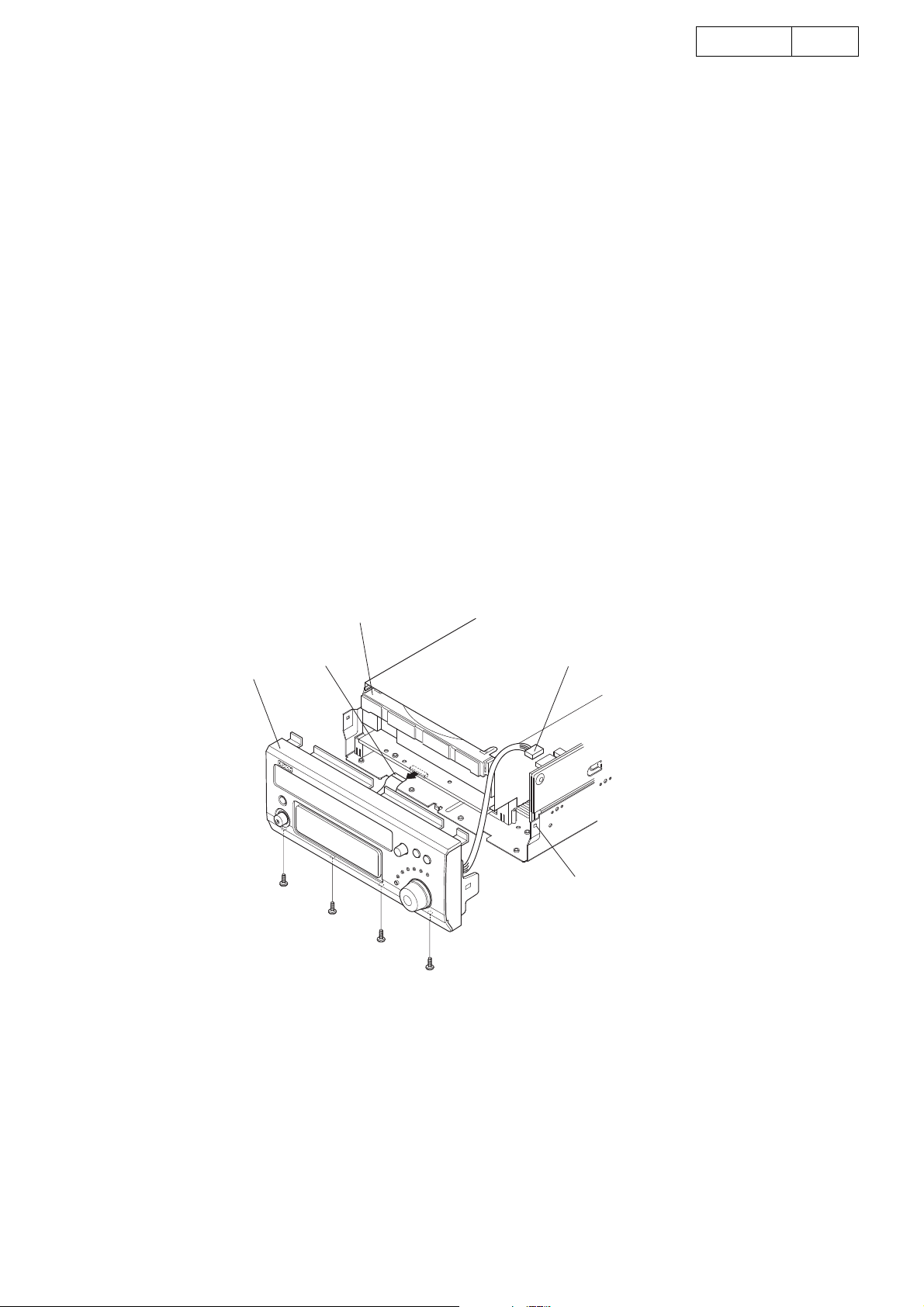
2. FRONT PANEL
(1)Disconnect FFC and 3p WIRG on the P.W.B..
(2)Remove 4 lower screws.
(3)Detach the Front Panel with releasing the hook on both
sides.
各部のはずしかた
(組み立てるときは、逆の順序でおこなってください。)
1. トップカバーのはずしかた
両サイドのからねじ 2本、リアパネルからのねじ 4本を
はずし、トップカバーを上にはずします。
2. フロントパネルのはずしかた
(1)基板から、FFC と 3P ワイヤをはずします。
(2)FRONTPANELの下側からねじ 4 本をはずします。
(3)両サイドの HOOK をはずし、FRONTPANEL をはずし
ます。
FRONT PANEL
DVD MECHA
FFC
3P WIRG
HOOK
3
Page 4
ADV-M71
4
3. DVD MECHANISM UNIT
(1)Remove 5 screws to detach the MECHA COVER and
the DVD Mecha.
(2)Disconnect WIRG from the DVD Mecha.
DVD MECHA
3. DVDメカのはずしかた
(1)ねじ 6 本をはずし、MECHACOVERとDVDMECHA-
EARTHCLIPをはずします。
(2)DVDMECHAからワイヤをはずします。
MECHA COVER
4. REAR PANEL
(1)Pull out the cord bush.
(2) Remove 26 screws.
EARTH CLIP
4. リアパネルのはずしかた
(1)CORDBUSHをはずします。
(2)ねじ 26 本をはずします。
CORD BUSH
4
Page 5
ADV-M71
5
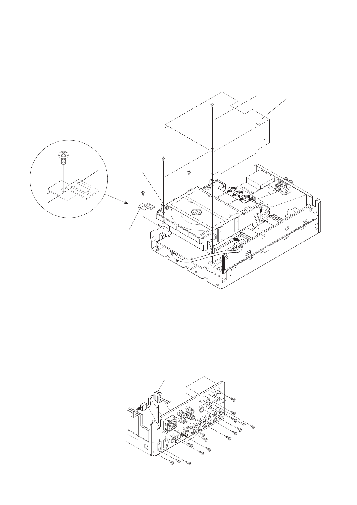
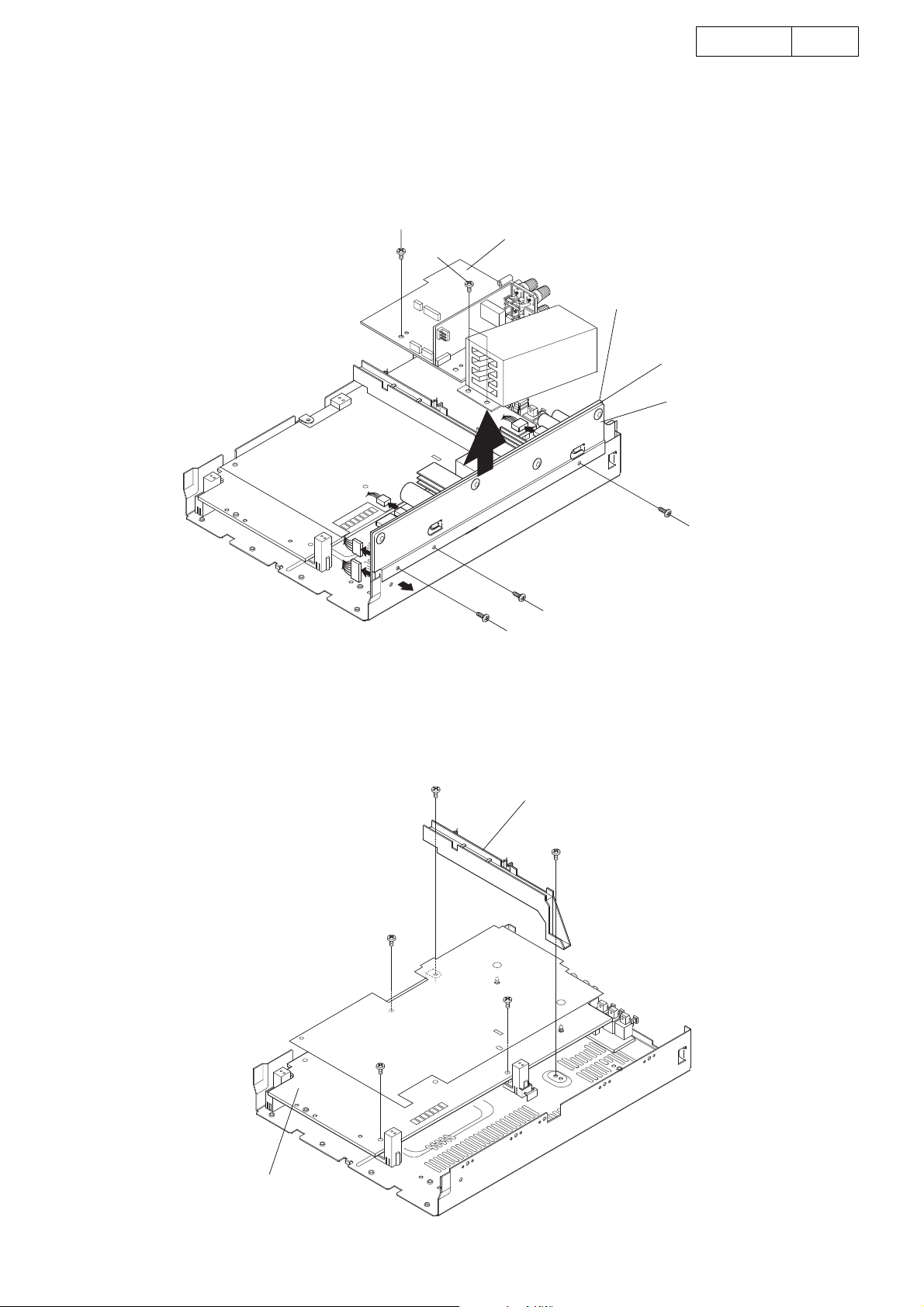
5. POWER P.W.B. / AMP VIDEO P.W.B.
(1)Remove 3 screws to detach the P.W.B. BRACKET
together with the POWER P.W.B..
(2)Unplug 4 connectors on the POWER P.W.B..
(3)Remove 3 screws.
(3)
5. パワー基板/アンプビデオ基板
(1)ねじ 3 本をはずし、POWERP.W.B.といっしょにP.W.B.
BRACKETをはずします。
(2)POWERP.W.B.のコネクタ4か所をはずします。
(3)ねじ3本をはずします。
AMP VIDEO P.W.B.
(3)
POWER P.W.B.
PVC SHEET
P.W.B. BRACKET
6. MAIN P.W.B.
(1)Remove 2 screws fixing the P.W.B. stay.
(2)Remove 3 screws.
(1)
(1)
(1)
メイ
6.
ン基板
(1)P.W.B.STAYを止めているねじ2本をはずします。
(2)ねじ 3 本をはずします。
P.W.B. STAY
MAIN P.W.B.
5
Page 6
ADV-M71
6
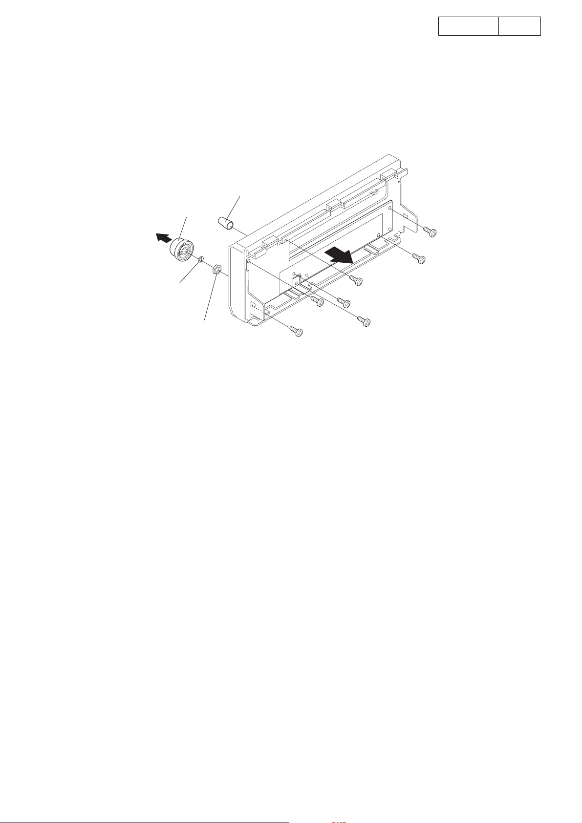
7. DISPLAY P.W.B.
(1)Pull out the VR knob and TUNING knob.
(2)Remove the spacer and the VR nut.
(3)Remove 7 screws.
VR KNOB
SPACER
VR NUT
7. ディスプレイ基板
(1)VRKNOBとTUNINGKNOBをはずします。
(2)SPACERとVRNUTをはずします。
(3)ねじ7本をはずします。
TUNNING KNOB
6
Page 7
g
RGB_H
p
(
)
50/60
BACK END DSP
YUV[0-7]
C
g
Pr/C
CS
AUDIO DECODER
M66005AFP
RESET
D.D/DTS/PCM/AAC
(
))
VR-JOG
KEY
KEY-0/1
D
V.MUTE 1/2YY/C
ROTARY ENCODER
byMONITOR OUT
16MB
DelayC
CLK
SPDIF OUT
I/O1䌾I/O7
DIR
OPT IN 1
RXOUT
LC89057
DI/DO/CE/CLK
STEREO
DI/DO/CE/CLK/RST
SYR
AUDIO/EMPHA/INT
DATA
VR MUTE
FL/FR
CLK
C
FM ANT
SL/SR
RELAY FR
[+6dB]
[0dB]
FL
PASS
POWER AMP
TU.MUTE
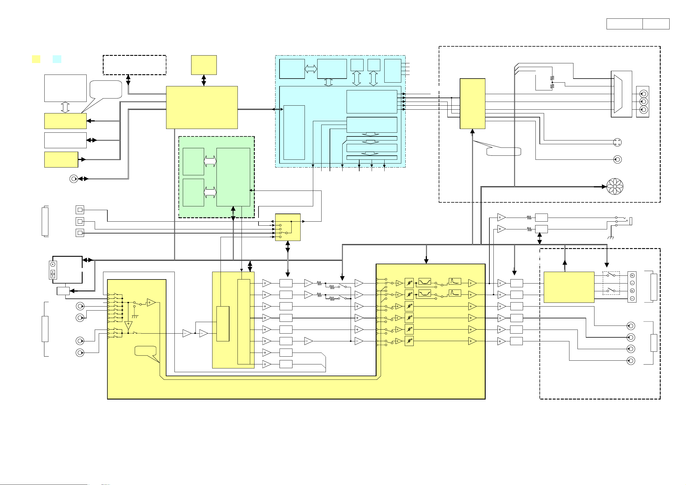
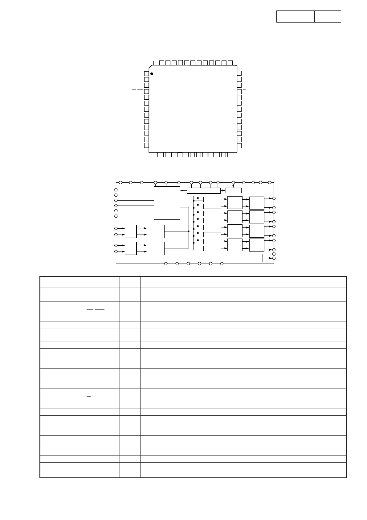
BLOCK DIAGRAMS
ADV-M71
7
:IC :DVD Engine Block
FL TUBE P ON/OFF
HNV-15SS04T SUB ON/OFF
13digit Dot Matrix SYSTEM uCOM ES6028 PY/Y
DISC information is
received from DVD
and it displays it in the
FL tube.
SWITCHING POWER SUPPLY EEPROM PROG/INTE
16k
DVD ON/OFF DI/DO/CS/CK
M30626 FHPGP
CLK
FL DRIVER DA/CK/CE/RST
SDATA I/O
A/B TBCK
LED LED-G DENON BASS Management
REMOCON REMOTE
GP1UE271XK AUDIO DSP MONITOR OUT
DENON BUS
x2
Communicate with DENON-BUS : MD/DECK/CD-R 64MB
OPT OUT RESET/ACK/REQUEST/BUSY NJM4556AD
[GP1Z352TZ] WRIGHT/OSC/IOPOWER/POM_RST
[GP1F352RZ] SPDIF SDATA
OPT IN 2 DIN 0 RBCK
DIGITAL IN/OUTAUDIO IN/OUT
[GP1F352RZ] PCM MCLK H/P MUTE
LED-R
ROM
RXD ADSST-MEL100 SPDIF RSD TSD3 TSD 2 TSD 1 TSD 0
TXD
MELODY 100
SD-RAM FAN ON/OFF COOLING FAN
PCM/AAC/D.D/DTS bitstream SPDIF RWS
DVD ENGINE UNIT RL-871 1U-3528 AMP/POWER UNIT
DVD MECHA ROM RAM
PU/Traverse FRONT END
Loadin
User I/F
Developed
( MCLK)
TWS
VIDEO DAC 4ch
with Pro
ressive scan
PLII/MP3/(WMA)/2chVirtual
PPCM(DVD-Audio
ownMix
Config-1(ON/OFF each CH)
for VDAC ex
UD-M30DVx : no use
Pb/Cb
and VIDEO DRIVER
r
with Filter
PY IN
Pb IN
Pr IN
YIN
CIN
BH7862
MIXOUT
C OUT
PY/Y
Pb/Cb
Pr/Cr
Y
C
V
Mute PY/Pb/Pr or Y/C/V
constantly
PCM/D.D/DTS bitstream H/P AMP
1U-3527 MAIN UNIT
VCNT1/YC_H
VCNT2/WIDE
MUTE
MUTE
LINE_2
LINE_3
J:D-TERMINAL VIDEO OUT
C
omposite
H/P SW
E3:COMPONENT VIDEO OUT
H/P
TUNED [I2S x 3] ERR/CS FLAG/96DET
FM/AM SDATA(AD) DO/CE/CLK/RST ERR MUTE SUB SUM
AM ANT NJM2068 BA15218 BA15218 DSP/EXT/DIRECT BASS/TREBLE SDB
TUNER PACK LRCK/BCK for SP Config-2 SWITCHING
VR
㪤㪬㪫㪜
MUTING
LINE-1 IN C
MUTE
LINE-2 IN SL
LINE-1 OUT LFE
LINE-2 OUT AD1837 DMIXL [0dB] 4.2Vrms
Route of
DIRECT mode
BA15218
A/D CONVERTER
8ch CODEC
㪏㪺㪿㩷㪛㪆㪘㩷㪚㪦㪥㪭㪜㪩㪫㪜㪩
FR
㪤㪬㪫㪜
㪤㪬㪫㪜
㪤㪬㪫㪜
SR
㪤㪬㪫㪜
㪤㪬㪫㪜
㪤㪬㪫㪜
DMIXR FUNCTION/VR/TONE/SDB IC
for RECOUT
㪤㪬㪫㪜
INPUT GAIN AMP
0/+6dB
BD3811K1
OUTPUT GAIN
0䌾+18dB
2dBstep BA15218
Max output
PRE AMP
MUTE
MUTE
MUTE
MUTE
MUTE
MUTE
SW
[STK-402-050]
1U-3528 AMP/POWER UNIT
PROTECT
THERMO
FL
FR
SW
C
SL
SR
SPEAKER OUT
PRE OUT
7
Page 8
LEVEL DIAGRAMS
DIGITAL
OPT IN
-20dBFs
DIR
DSP
ADV-M71
8
POWER AMPPRE AMP
ANALOG
LINE IN
200mVrms
ANALOG
DIGITAL
L,R
L/R ch
FL/FR ch
SL/SR/C ch
ANALOG ANALOG DIRECT
-6dB
To A/D
470
470
2ch
A/D
AD1837
8ch CODEC
0dBFs
=1Vrms
-10dBFs
-20dBFs
-23dB
8ch
D/A
FL/FR
SL/SR/C
SW
ANALOG DIRECT
Prologic
+6dB
MUTE
MUTE
MUTE
For
Config2
TONE
SDB
BD3811
ELEC. VR
ELEC. VR Head Room (4.2Vrms)
26.4dB
-18dB
-15dB
Prologic
at VR "00"
FL/FR
SL/SR/C
SW
+6dB
+10dB
+19dB
PRE AMP Head Room (7.0Vrms)
21.0dB
SL/SR/C
+10dB
+6dB
FL/FR
MUTE
MUTE
MUTE
30dB
30dB
SL/SR/C
SW
SP OUTFL/FR
VR MAX: 12.6Vrms
VR MAX : 632mVrms
VR " 00 " : 80mVrms
FL/FR
(20W, 8Ω)
SW ch
Input Sens : 200mVrms
SP Output Power : 20W (THD 0.08%,8Ω)
Total GAIN : 36dB
0dBFs
=1Vrms
-10dBFs
-20dBFs
-30dBFs
-35dBFs
+6dB
+2.85dB
PRE AMP Head Room (7.0Vrms)
ELEC. VR Head Room (4.2Vrms)
21.0dB
VR MAX : 632mVrms
VR " 00 " : 80mVrms
Config-1
+7.5dB
+3.31dB
Config-2
To Front ch
-18dB
atVR"00"
8
Page 9
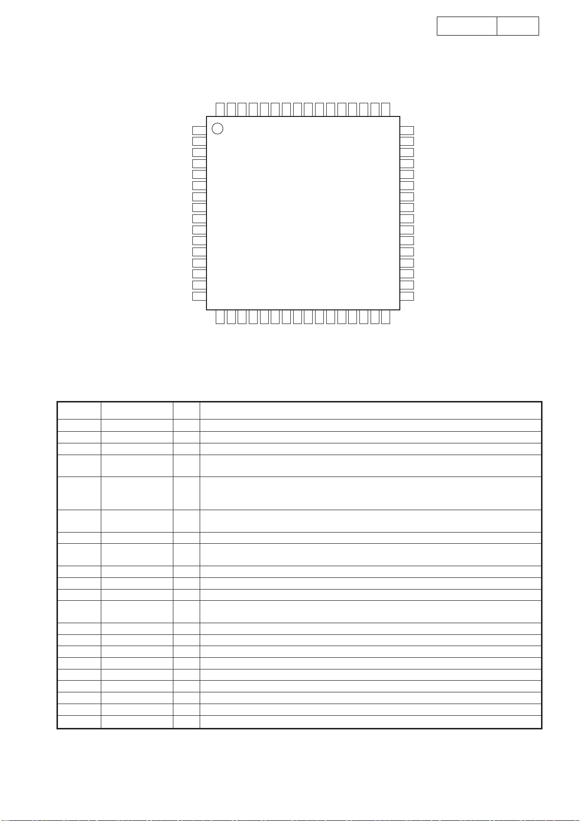
SEMICONDUCTORS
Only major IC's are shown, general IC's etc. are omitted to list.
主な半導体を記載しています。汎用の半導体等は記載を省略しています。
●IC's
Note: Abbreviation ahead of IC No. indicates the name of P.W.B., etc.
注 ) : IC No. の前の記号は、基板の名称を表します。
DS : DSP P.W.B. AP: AMP/POWER P.W.B.
MA: Main P.W.B. ME : MECHA P.W.B.
ADSST-MEL100(DS:IC801)
Note : When this IC is defecitive, replace P.W.B. Unit Ass'y
TOP VIEW
ADV-M71
123456789101112131415
A
B
C
D
E
F
G
H
J
K
L
M
N
P
R
9
ADSST-MEL100 Terminal Function
Pin Name
NC A01
BMSTR A02
BMS_B A03
SPIDS A04
EBOOT A05
LBOOT A06
SCLK2 A07
SD3B A08
L0DAT[4] A09
L0ACK A10
L0DAT[2] A11
L1DAT[6] A12
L1CLK A13
L1DAT[2] A14
NC A15
FLAG10 E01
RESET_B E02
FLAG8 E03
SD0A E04
VDDEXT E05
VDDINT E06
VDDEXT E07
VDDINT E08
VDDEXT E09
VDDINT E10
VDDEXT E11
L0DAT[0] E12
DATA[39] E13
DATA[43] E14
TRST_B B01
TD1 B02
RPBA B03
MOSI B04
Pin No.
Pin Name
SFS0 B05
SCLK1 B06
SD2B B07
SD3A B08
L0DAT[7] B09
L0CLK B10
L0DAT[1] B11
L1DAT[4] B12
L1ACK B13
L1DAT[0] B14
NC B15
FLAG5 F01
FLAG7 F02
FLAG9 F03
FLAG6 F04
VDDINT F05
GND F06
GND F07
GND F08
GND F09
GND F10
VDDINT F11
DATA[37] F12
DATA[40] F13
DATA[38] F14
TMS C01
EMU_B C02
GND C03
SPICLK C04
SD08 C05
SD1A C06
SD2A C07
SFS2 C08
Pin No.
Pin Name
SFS3 C09
L0DAT[6] C10
L1DAT[7] C11
L1DAT[3] C12
L1DAT[1] C13
DATA[45] C14
DATA[47] C15
FLAG1 G01
FLAG2 G02
FLAG4 G03
FLAG3 G04
VDDEXT G05
GND G06
GND G07
GND G08
GND G09
GND G10
VDDEXT G11
DATA[34] G12
DATA[35] G13
DATA[33] G14
DATA[41] E15
IRQ2_B J01
ID1 J02
ID2 J03
ID0 J04
VDDEXT J05
GND J06
GND J07
GND J08
GND J09
GND J10
VDDEXT J11
Pin No.
Pin Name
DATA[26] J12
DATA[24] J13
DATA[25] J14
DATA[27] J15
ADDR[14] N01
ADDR[15] N02
ADDR[10] N03
ADDR[5] N04
ADDR[1] N05
MS0_B N06
BR5_B N07
BR2_B N08
BRST N09
SDCKE N10
CS_B N11
CLK_CFG1 N12
CLK_CFG0 N13
AVDD N14
DMARI1_B N15
DATA[36] F15
TIMEXP K01
ADDR[22] K02
ADDR[20] K03
ADDR[23] K04
VDDINT K05
GND K06
GND K07
GND K08
GND K09
GND K10
VDDINT K11
DATA[22] K12
DATA[19] K13
Pin No.
BOTTOM VIEW
Pin Name
DATA[21] K14
DATA[23] K15
ADDR[13] P01
ADDR[9] P02
ADDR[8] P03
ADDR[4] P04
MS2_B P05
SBTS_B P06
BR4_B P07
BR1_B P08
SDCLK1 P09
SDCLK0 P10
REDY P11
CLKIN P12
DQM P13
AVSS P14
DMAR2_B P15
DATA[32] G15
ADDR[19] L01
ADDR[17] L02
ADDR[21] L03
ADDR[2] L04
VDDEXT L05
VDDINT L06
VDDEXT L07
VDDINT L08
VDDEXT L09
VDDINT L10
VDDEXT L11
CAS_B L12
DATA[20] L13
DATA[16] L14
DATA[18] L15
Pin No.
Pin Name
NC R01
ADDR[11] R02
ADDR[7] R03
ADDR[3] R04
MS3_B R05
PA_B R06
BR3_B R07
RDL_B R08
CLKOUT R09
HBR_B R10
HBG_B R11
CLKDBL R12
XTAL R13
SDWE_B R14
NC R15
DATA[31] H15
ADDR[16] M01
ADDR[12] M02
ADDR[18] M03
ADDR[6] M04
ADDR[0] M05
MS1_B M06
BR6_B M07
VDDEXT M08
WRL_B M09
SDA10 M10
RAS_B M11
ACK M12
DATA[17] M13
DMAG2_B M14
DMAG1_B M15
Pin No.
9
Page 10
ES6028 (ME: U9)
VSS
HA1
156
VEE
HA2
VEE
AUX[0]
AUX[1]
AUX[2]
VSS
VEE
AUX[3]
AUX[4]
AUX[5]
AUX[6]
AUX[7]
LOE#
VSS
VCC
LCS0#
LCS1#
LCS2#
LCS3#
VSS
VEE
VSS
LD10
LD11
VSS
VEE
LD12
LD13
LD14
LD15
LWRLL#
LWRHL#
VSS
VEE
CAMIN0
CAMIN1
VSS
LD0
LD1
LD2
LD3
LD4
LD5
LD6
LD7
LD8
LD9
LA0
LA1
LA2
LA3
155
157
158
159
160
161
162
163
164
165
166
167
168
169
170
171
172
173
174
175
176
177
178
179
180
181
182
183
184
185
186
187
188
189
190
191
192
193
194
195
196
197
198
199
200
201
202
203
204
205
206
207
208
123456789101112131415161718192021222324252627282930313233343536373839404142434445464748495051
HA0
154
HCS3FX#
HCS1FX#
153
152
VEE
VSS
DSCK
DQM
DCS0#
VEE
VSS
DCS1#
DB15
DB14
DB13
DB12
VEE
VSS
DB11
DB10
DB9
DB8
DB7
DB6
VSS
VCC
DB5
DB4
DB3
DB2
DB1
DB0
VSS
VEE
DMBS1
DMBS0
DRAS#
DWE#
DSCK_EN
DCAS#
VEE
VSS
DMA11
DMA10
DMA9
DMA8
DMA7
DMA6
VSS
VEE
DMA5
DMA4
DMA3
DMA2
DMA1
DMA0
10
ADV-M71
HIOCS16#
HRD#
HWR#
VEE
VSS
HIORDY
HRST#
HIRQ
HRDQ#
HWRQ#
HD15
HD14
VCC
VSS
HD13
HD12
HD11
HD10
HD9
HD8
HD7
VEE
VSS
HD6
HD5
HD4
HD3
HD2
HD1
HD0
VCC
VSS
HSYNC#
VSYNC#
PCLKQSCN
PCLK2XSCN
YUV7
YUV6
YUV5
VSS
ADVEE
YUV4
YUV3
YUV2
YUV1
YUV0
DCLK
151
150
149
148
147
146
145
144
143
142
141
140
139
138
137
136
135
134
133
132
131
130
129
128
127
126
125
124
123
122
121
120
119
118
117
116
115
114
113
112
111
110
109
108
107
106
105
104
103
102
101
100
99
98
97
96
95
94
93
92
91
90
89
88
87
86
85
84
83
82
81
80
79
78
77
76
75
74
73
72
71
70
69
68
67
66
65
64
63
62
61
60
59
58
57
56
55
54
53
52
LA4
LA5
LA6
LA7
LA8
VEE
LA9
VSS
VCC
VSS
LA10
LA11
LA12
LA13
VEE
LA14
LA15
LA16
LA17
ES6038 Terminal Function
1, 18, 27, 59,
68, 75, 92, 99,
104, 130, 148, VEE I I/O power supply.
157, 159, 164,
183, 193, 201
8, 17, 26, 34,
43, 52, 60, 67,
76, 84, 91, 98,
103, 112, 120, VSS I Ground.
129, 138, 147,
156, 163, 171,
177, 184, 192,
200, 208
23:19, 16:10,
7:2, 207:204
9, 35, 44, 83,
121, 139, 172
LA[21:0] O Device address output.
VCC I Core power supply.
TDMFS
TDMTSC#
VSS
VCC
TSD2
TWS/SEL_PLL2
TSD0/SEL_PLL0
TSD1/SEL_PLL1
VSS
LA18
LA19
LA20
VEE
LA21
TDMDX
TDMDR
RESET#
TDMCLK
NC
TSD3
VSS
TBCK
MCLK
SPDIF/PLL3
VCC
RSD
RWS
RBCK
NC
XIN
VSS
AVEE
XOUT
FunctionI/OPin No. Pin Name
10
Page 11
ADV-M71
11
Pin No. Pin Name
24 RESET# I Reset input, active low.
25 TDMDX O TDM transmit data.
28 TDMDR I TDM receive data.
29 TDMCLK I TDM clock input.
30 TDMFS I TDM frame sync.
31 TDMTSC# O TDM output enable.
TWS O Audio transmit frame sync.
SEL_PLL2 I System and DSCK output clock frequency selection is made at the rising edge of RESET#.
The matrix below lists the available clock frequencies and their respective PLL bit settings.
SEL_PLL2 SEL_PLL1 SEL_PLL0 Clock Type
0 0 0 VCO off.
0 0 1 DCLK
32 0 1 0 Bypass mode
0 1 1 DCLK x 2
1 0 0 DCLK x 4.5
1 0 1 DCLK x 3
1 1 0 DCLK x 3.5z
1 1 1 DCLK x 4
33
36
37 TSD[2] O Audio transmit serial data output 2.
38 TSD[3] O Audio transmit serial data output 3.
39 MCLK I/O Audio master clock for audio DAC.
40 TBCK O Audio transmit bit clock.
41 SEL_PLL3 Clock Source
42,48 NC No connect pins. Leave open.
45 RSD I Audio receive serial data.
46 RWS I Audio receive frame sync.
47 RBCK I Audio receive bit clock.
49 XIN I Crystal input.
50 XOUT O Crystal output.
51 AVEE I Analog power for PLL.
66:61, 58:53 DMA[11:0] O DRAM address bus [11:0]
69 DCAS# O DRAM column address strobe,
70 DSCK_EN O DRAM clock enable.
71 DWE# O DRAM write enable.
72 DRAS# O DRAM row address strobe.
73 DMBS0 O SDRAM bank select 0.
74 DMBS1 O SDRAM bank select 1.
96:93, 90:85,
82:77
97, 100 DCS[1:0]# O SDRAM chip select [1:0]
101 DQM O Data input/output mask.
102 DSCK O Output clock to SDRAM.
105 DCLK I 27 MHz clock input to PLL.
106 UDAC O Video UDAC output.
107 VREF I Internal voltage to video DAC.
108 CDAC O Video CDAC output.
109 COMP I Compensation input.
110 RSET I DAC current adjustment resistor input.
111 ADVEE I Analog power for video DAC.
113 YDAC O Video YDAC output.
TSD0 O Audio transmit serial data port 0.
SEL_PLL0 I Refer to the description and matrix for SEL_PLL2 pin 32.
TSD1 O Audio transmit serial data port 1.
SEL_PLL1 I Refer to the description and matrix for SEL_PLL2 pin 32.
SPDIF O S/PDIF output.
SEL_PLL3 I Clock source select.
0 Crystal oscillator
1 DCLK input
DB[15:0] I/O DRAM data bus [15:0]
FunctionI/O
11
Page 12
ADV-M71
12
Pin No. Pin Name
114 VDAC O Video VDAC output.
115 YUV7 O YUV7 pixel output data.
116 PCLK2XSCN I/O 27 MHz video output pixel clock.
117 PCLKQSCN O 13.5 MHz video output pixel clock.
118 VSYNC# I/O Ver tical sync, active low.
119 HSYNC# I/O Horizontal sync, active low.
127:122 HD[5:0] I/O Host data I/O [5:0].
128 HD[6] I/O Host data I/O [6].
131 HD[7] I/O Host data I/O [7].
132 HD[8] I/O Host data bus 8.
133 HD[9] I/O Host data bus line 9.
134 HD[10] I/O Host data bus line 10.
135 HD[11] I/O Host data bus line 11.
136 HD[12] I/O Host data bus line 12.
137 HD[13] I/O Host data bus line 13.
140 HD[14] I/O Host data bus line 14.
141 HD[15] I/O Host data bus line 15.
142 HWRQ# O Host write request.
143 HRRQ# O Host read request.
144 HIRQ I/O Host interrupt.
145 HRST# O Host reset.
146 HIORDY I Host I/O ready.
149 HWR# I/O Host write.
150 HRD# O Host read.
151 HIOCS16# I Device16-bit data transfer.
152 HCS1FX# O Host select 1.
153 HCS3FX# O Host select 3.
158, 155:154 HA[2:0] I/O Host address bus.
160 AUX[0] O I2C DATA.
162 AUX[2] I/O Auxiliary ports 2.
165 AUX[3] I/O Auxiliary ports 3.
169:166 AUX[7:3] I/O Auxiliary ports 7:3.
170 LOE# O Device output enable.
176:173 LCS[3:0]# O Chip select [3:0].
197:194,
191:185, LD[15:0] I/O EPROM device data bus.
182:178
198 LWRLL# O Device low-byte write enable.
199 LWRHL# O Device high-byte write enable.
202 CAMIN0 I Camera YUV 0.
203 CAMIN1 I Camera YUV 1.
161 AUX[1]OI2C CLK.
FunctionI/O
12
Page 13
M5705 (ME: U1)
AVSS-DS
XSRFIN
XSIPIN
AVDD5-DS
XSDSSLV
XSRSLINT
XSAWRC
XSRFGC
XSEFGC
XSFOCUS
XSTRACK
XSSLEG
AVDD5-DA
XSMOTOR
AVSS-DA
XSRFRPLP
XSTELP
XSVREF2
XSRFRP
XSTEXI
AVSS-AD
XSTEI
XSFEI
XSAEI
AVDD5-AD
XSSBAD
GND
XSDFCT
XSCSJ
XSCLK
XSDATA
XSLDC
XSFGIN
XSSPDON
XSFLAG(3)
XSFLAG(2)
XSFLAG(1)
XSFLAG(0)
XMP1_7
XMP1_6
GND
XMP1_4
XSAWRCVCO
XSVREFO
XSPDOFTR2
XSVR_PLL
XSFTROPI
XSFDO
AVSS_PL
XSPLLFTR2
AVDD5_PL
XSFDIREF
XSPDIREF
GND
XTSLRF
XTPLCK
VDD
XRA(3)
XRA(2)
XRA(1)
XRA(0)
XRA(4)
XRA(5)
XRA(6)
GND
XRA(7)
XRA(10)
XRA(11)
VDD
XRA(8)
XRA(9)
XROEJ
VDD
176
175
174
173
172
171
170
169
168
167
166
165
164
163
162
161
160
159
158
157
156
155
154
153
152
151
150
149
148
147
1
2
3
4
5
6
VDD
7
8
9
10
11
12
13
14
15
16
17
18
19
20
21
22
23
24
25
26
27
28
29
30
31
32
33
34
35
36
37
38
39
40
41
42
NC
43
44
45464748495051525354555657585960616263646566676869707172737475767778798081828384858687
VDD
VDD
GND
XOSC1
XOSC2
XMALE
XMD(0)
XMD(1)
XMD(2)
XMD(3)
XMD(4)
XMD(5)
XMD(6)
XMP1_3
XMFSCSJ
XMP1_2
XGPIO(2)
XMP1_1
XMRSTJ
XGPO(1)
XGPO(0)
XCRSTJ
XMPSENJ
XMP1_0
XMD(7)
146
XMCSJ
XMRDJ
XMWRJ
XMA(11)
XMA(10)
XMINT1J
4M DRAM
M5705
XRCASJ
XRRASJ
145
144
VDD
XMA(9)
XRSDCLK
XRWEJ
143
142
XMA(8)
XMA(7)
XRD(7)
141
XMA(6)
XRD(8)
140
XMA(5)
XRD(6)
139
XMA(4)
GND
138
XMA(3)
XRD(9)
137
XMA(2)
XRD(5)
136
XMA(1)
XRD(10)
XRD(4)
135
134
XMA(0)
XMA(12)
XRD(11)
133
132
131
130
129
128
127
126
125
124
123
122
121
120
119
118
117
116
115
114
113
112
111
110
109
108
107
106
105
104
103
102
101
100
88
GND
99
98
97
96
95
94
93
92
91
90
89
XRD(3)
XRD(12)
GND
XRD(2)
XRD(13)
XRD(1)
XRD(14)
XRD(0)
XRD(15)
XHD(7)
XHD(8)
XHD(6)
XHD(9)
XHD(5)
XHD(10)
XHD(4)
XHD(11)
VDD
XHD(3)
XHD(12)
XHD(2)
XHD(13)
GND
XHD(1)
XHD(14)
XHD(0)
XHD(15)
XHDRQ
XHIOWJ
XHIORJ
XHIORDY
XHDACKJ
XHINT
XHCS16J
XHA(1)
XHPDIAGJ
XHA(0)
XHA(2)
XHCS1J
XHCS3J
XHDASPJ
XMA(15)
XMA(14)
XMA(13)
ADV-M71
13
ATAPI
M
Motor
Driver
Data
Separator
Digital
Servo
DVD-DSP
CD-DSP
RAM
Arbiter
Target
Search
&
MPEG
I/F
C3 ECC
EDC
MCU
ROM
M5705 Terminal Function
Pin Name
Type
2 XSRFIN I/A Analog RF signal input after passing through the equalizer
3 XSIPIN I/A Inverting input pin of data slicer
5 XSDSSLV O/A Slice level output pin
6 XSRSLINT I/A Reference current setting pin for analog data slicer
8 XSAWRC O/A Output for enlarge VCO range. Analog output from DAC buffer
9 XSRFGC O/A RF gain control output
10 XSEFGC O/A E,F gain control output
11 XSFOCUS O/A Output voltage level for focusing buffer IC
12 XSTRACK O/A Output voltage level for tracking buffer IC
13 XSSLEG O/A Output voltage level for sledge buffer IC
15 XSMOTOR O/A Output voltage level for spindle motor buffer IC
17 XSRFRPLP I/A High bandwidth low pass filter input for RFRP
18 XSTELP I/A High bandwidth low pass filter input for TE
19 XSVREF2 I/A 2.1V reference voltage input
20 XSRFRP I/A RF ripple/envelope signal input
21 XSTEXI I/A Tracking zero crossing input signal
23 XSTEI I/A Tracking error input signal
24 XSFEI I/A Focus error input signal
25 XSCEI I/A
1. Center error input signal
2. Photo Interrupt input
DescriptionPin No.
PC
MPEG
DEC.
13
Page 14
ADV-M71
14
Pin Name
27 XSSBAD I/A Sub-beam addition signal input
166 XSPDIREF I/A
167 XSFDIREF I/A
169 XSPLLFTR2 I/A Data PLL loop filter pin#2
171 XSFDO O/A Output node of frequency detector charge pump circuit
172 XSFTROPI I/A Input node of loop filter OP circuit
173 XSVR_PLL I/A PLL reference voltage input
174 XSPDOFTR2 I/A Phase detector filter pin#1
175 XSVREFO O/A Reference voltage output
176 XSAWRCVCO I/A Auto Wide Range Control of VCO input pin. For enlarge VCO range in CAV mode
29 XSDFCT I Detect detection signal input
30 XSCSJ O Chip select signal for accessing control registers
31 XSCLK O Clock output for accessing control registers
32 XSDATA I/O Registers data input/output pin
33 XSLDC O Laser diode on/off control output for both CD/DVD
34 XSFGIN I Motor Hall sensor input
35 XSSPDON O Spindle motor on output
36, 37, 38, 39 XSFLAG[3:0] O These pins are used to monitor some status of servo control block
48, 51, 52 XGPIO[2:0] I/O
40 XMP1_7 I/O Internal microcontroller programmable I/O port 1.7.
41 XMP1_6 I/O Internal microcontroller programmable I/O port 1.6.
43 XMP1_5 I/O This pin is now changed to be NC.
44 XMP1_4 I/O Internal microcontroller programmable I/O port 1.4.
45 XMP1_3 I/O Internal microcontroller programmable I/O port 1.3.
47 XMP1_2 I/O Internal microcontroller programmable I/O port 1.2.
49 XMP1_1 I/O Internal microcontroller programmable I/O port 1.1.
57 XMP1_0 I/O
46 XMFSCSJ I/O Output chip select connected to external flash ROM chip enable pin
54 XMPSENJ I/O Output program store enable connected to external ROM PSENJ pin.
56 XMALE I/O This signal is used as address latch signal in address/data mux mode
70 XMCSJ I/O
71 XMRDJ I/O
72 XMWRJ I/O This signal is used as the Wire Strobe signal
73 XMINT1J I/O
74, 75, 77, 78,
79, 80, 81, 82,
83, 84, 85, 86,
87, 89, 90, 91
62, 63, 64, 65,
66, 67, 68, 69 bus for the 8-bit processor mode.
163 XTPLCK I/O PLCK test pin
164 XTSLRF I/O SLRF test pin
59 XOSC1 I Crystal input/System clock. The input frequency from outside crystal or oscillator is 33.8688MHz
60 XOSC2 O Crystal output
53 XCRSTJ I
94 XHCS1J I This pin is used to select the command block task file registers
93 XHCS3J I This pin is used to select the control block task file registers
103 XHIORJ I Asserted by the host during a host I/O read operation
104 XHIOWJ I Asser ted by the host during a host I/O write operation
105 XHDRQ O
101 XHDACKJ I
99 XHCS16J O
50 XHRSTJ I Host Reset. The reset of ATA bus
100 XHINT O
XMA[15:0] I/O These pins are used as address bus
XMD[7:0] I/O
Type
Phase detector reference current generator. Connect a resistor between this pin and
ground to set reference current
Frequency detector reference current generator. Connect a resistor between this pin and
ground to set reference current
1. These pins are used as general purpose I/O bus
2. When use internal microcontroller, XGPIO[2] can be used as programmable I/O port 3.6.
Internal microcontroller programmable I/O port 1.0.
This pin is default used as the A16 (microcontroller address line 16)
1. This signal must be asserted for all microcontroller accesses to the register of this chip
2. When use internal microcontroller, this signal can be used as programmable I/O port 3.1
1. This signal is used as the Read Strobe signal
2. When use internal microcontroller, this signal can be used as programmable I/O port 3.0
1. This signal is an interrupt line to the microcontroller
2. When use internal microcontroller, this signal can be used as programmable I/O port 3.7
These pins are used as data bus for the 16-bit processor mode, or the address/data mux
Chip Reset. As asserted low input generates a component reset that stops all operations within
the chip and deasserts all output signals. All input/output signals are set to input.
1.
DMA request. This pin is configured as the DMA request signal, and is used during DMA transfer
between the host and the controller. This pin is tri-stated when DMA transfers are not enabled.
2.
MPEG acknowledge. This pin is used as the ACKJ signal when MPEG interface mode is selected.
1. DMA acknowledge. This pin is configured as DACKJ, and is used as the DMA acknowledge
signal during DMA data transfers.
2. MPEG request. This pin is used as the REQ signal when MPEG interface mode is selected
1. 16-bit data select. This signal indicates that a 16-bit data transfer is active on the host data
bus. This pin is open-drain tri-state output.
2. MPEG clock. This pin is used as the CLOCK signal when MPEG interface mode is selected.
1. Host interface request. This tri-state pin is the host interrupt request, and is asserted to
indicate to the host that the controller needs attention.
2. MPEG begin. This pin is used as the BEGIN signal when MPEG interface mode is selected
DescriptionPin No.
14
Page 15
ADV-M71
15
Pin Name
97 XHPDIAGJ I/O This pin is used as the Passed Diagnostics signal, and may be an input or an open-drain output
92 XHDASPJ I/O
102 XHIORDY I/O
95, 96, 98 XHA[2:0] I
106, 107, 108, 2.
109, 111, 112, 3. VCD I/F. Bit3-0 are used as VCD I/F signal when VCD function is enabled. The relationship of
113, 114, 116, bit3-0 and VCD I/F is as follow
117, 118, 119, HD0—CD-DATA
120, 121, 122, HD1—CD-LRCK
123 HD2—CD-BCK
143 XRSDCLK O This signal is the clock output for SDRAM
147 XROEJ O
142 XRWEJ O This signal is asserted low when a buffer memory write operation is active
144 XRRASJ O
145 XRCASJ O
148, 149, 151,
152, 153, 155,
156, 157, 158,
159, 160, 161
124, 125, 126,
127, 128, 129,
131, 132, 134,
135, 136, 137,
138, 139, 140,
141
4 AVDD5_DS Analog Power +5V for Data Slicer part
14 AVDD5_DA Analog Power +5V for DAC part
26 AVDD5_AD Analog Power +5V for ADC part
168 AVDD5_PL Analog Power +5V for Data PLL part
7, 55, 58, 76,
115, 146,
150, 162
1 AVSS_DS Analog Ground for Data Slicer part
16 AVSS_DA Analog Ground for DAC part
22 AVSS_AD Analog Ground for ADC part
170 AVSS_PL Analog Ground for Data PLL part
28, 42, 61,
88, 110, 130,
138, 154, 165
XHD[15.0] I/O
XRA[11:0] O 1: Normal operation
XRD[15:0] I/O These signals are the 8-bit parallel data lines to/from the buffer memory.
VDD Power +3.3V for digital core logic and pad
GND Digital Ground core logic and pad.
Type
This pin is used as the Drive Active/Slave Present signal, and is an input or an open-drain
output. This pin is used for Master/Slave drive communication and/or for driving an LED
1. I/O channel ready. This signal is driven low to extend host transfer cycles when the controller
is not ready to respond. This pin will be tri-stated when a read or write is not in progress.
2. MPEG error. This pin is used as the ERROR signal when MPEG interface mode is selected
Host address lines. The host address lines A[2:0] are used to access the various host control,
status, and data registers
1. Host data bus. This bus is used to transfer data and status between the host and the controller.
MPEG data bus 7-8. The HD[7:0] are used as the DATA [7:0] when MPEG interface mode is selected.
HD3—CD-C2PO
This signal is used as the memory output enable for external DRAM buffers. After RSTJ is
asserted, this signal will be low
This signal is used as Row address output to external DRAM buffer. After RSTJ is asserted, this
signal will be high
This signal is used as column address output to external DRAM. After RSTJ is asserted, this
signal will be high
1. RAM address lines. These are bits11-0 for addressing the buffer memory.
2. Hardware setting. The bits6-0 are used as hardware setting for some functions.
RA[9] : FLASH size is 64K/128K
1: FLASH size is 64K
0: FLASH size is 128K
RA[8] : External CPU is 8032/H8
1: 8032
0: H8
RA[7] : Microcontroller programmable I/O port 1 pin control
1: By internal microcontroller
0: By registers to decide input/output
RA[6] : System test pin output
0: System test pin output
RA[5] : For testing purpose, don’t need to set
RA[4] : IDE master/slave
1: Slave
0: Master
RA[3] : For testing purpose, don’t need to set
RA[2] : For testing purpose, don’t need to set
RA[1-0] : MCU Mode selection
11: Normal Mode (internal uP, internal address latch)
10: Outside uP Mode (ICE Mode)
01: Test mode for internal uP testing
00: Internal uP mode with external address latch
DescriptionPin No.
15
Page 16
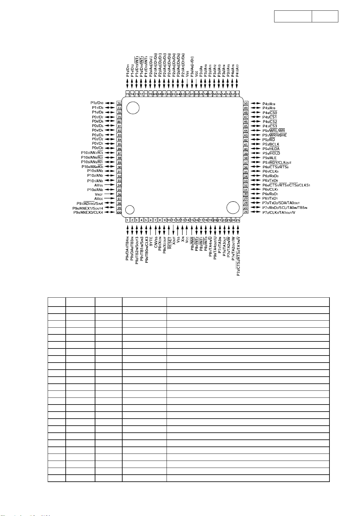
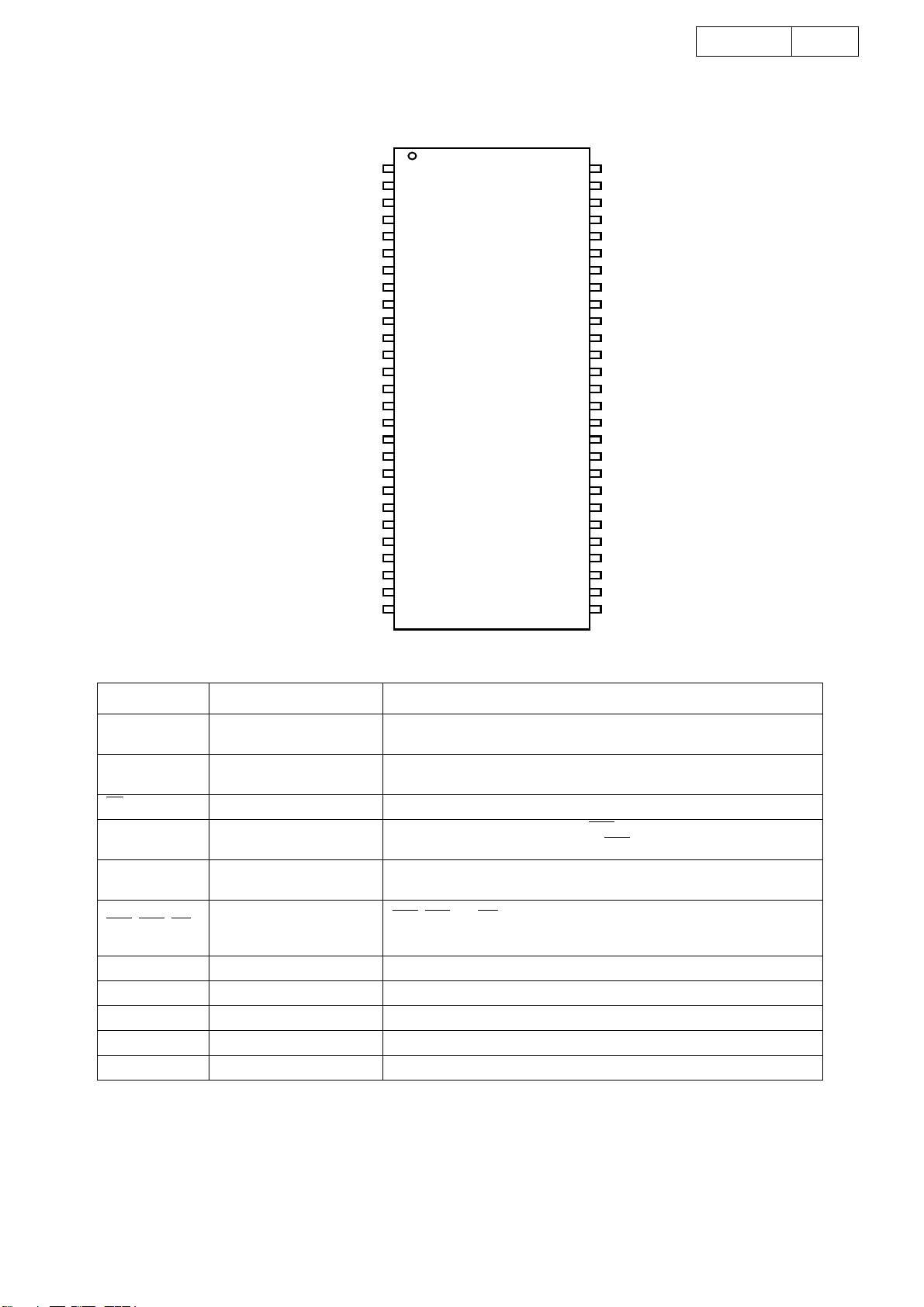
M30626FHPGP (MA: IC302)
ADV-M71
16
M30626FHPGP PORT
Pin No. port function Port setting Port name Explanation
1P94
2P93
3P92
4P91
5P90
6 BYTE - Gnd
7 CNVSS - don't use
8P87
9P86
10 RESET RESET Reset input
11 XOUT XOUT Xtal output
12 VSS VSS Gnd
13 XIN XIN Xtal input
14 VCC VCC Vcc
15 NMI - don't use
16 INT2
17 INT1
18 INT0 INT DE RXD Serial data input from DENON BUS
19 TA4IN
20 P80
21 P77
22 P76
23 P75
24 P74
25 P73
OE2P CS
O 3811 DATA
SO E2P DI
SI E2P DO
SO E2P CK
O 3811 CLK
OVMUTE
INT PROTECT
INT ESS CS
I50/60
O PROG/INTE
IVR JOG-B
IVR JOG-A
IFN JOG-B
IFN JOG-A
OFLCS
Chip select output to EEPROM
Serial data output to elec.VR
Serial data output to EEPROM
Serial data input from EEPROM
Serial clock output to EEPROM
Serial clock output to elec.VR
Mute output to video driver
Protect signal input L:Protect detect
Chip select input from ESS
Line pulse input(50/60Hz)
Progressive/Interlace switching signal output
VR encoder pulse-B input
VR encoder pulse-A input
Function encoder pulse-B input
Function encoder pulse-A input
Chip select output to FLD driver
16
Page 17

Pin No. port function Port setting Port name Explanation
26 CLK2
27 RXD2
28 TXD2
29 TXD1
30 P66 O DSPCOREPOW DSP(Mel100) core power ON/OFF switching H:P-ON
31 CLK1
32 P64
33 TXD0
34 RXD0
35 CLK0
36 P60
37 P57
38 P56
39 P55 O - don't use
40 P54
41 P53
42 P52 O RGB H Conposite/S/RGB switching
43 P51
44 P50 O - don't use
45 P47
46 P46
47 P45
48 P44
49 P43
50 P42
51 P41
52 P40
53 P37
54 P36
55 P35
56 P34
57 P33 O EXP OE for port expand
58 P32 O EXP STB for port expand
59 P31 O EXP DA for port expand
60 VCC VCC Vcc
61 P30 O EXP CLK for port expand
62 VSS VSS Gnd
63 P27
64 P26
65 P25
66 P24
67 P23
68 P22
69 P21
70 P20
71 INT5
72 INT4
73 INT3
74 P14
75 P13
76 P12
77 P11
78 P10
79 P07
80 P06
81 P05
82 P04
83 P03
84 P02
85 P01
SO DE CK
SI DE RXD
SO DE TXD
SO FLDA
SO FLCK
OFLRST
SO ESS DO
SI ESS DI
SI ESS CK
I ESS ON
ODVD RST
I HP SW
O
REQ1
O DVD ON/OFF
O VCONT1
O VCONT2
OCODEC RST
O SEL CLK
O BSE
OERR MUTE
ODIR CE
ODIR RST
OCLATCH
OP.ON/OFF
OSCART MUTE
OSUB ON
O FR-RELAY
I TEMP FAN
ISTEREO
ITUNED
OTMUTE
OTU CE
OTU DI
OTU CK
ITU DO
DFRES Ext reset signal from ESS
I
I DIR INT1
IREMOTE
O SYR
O DSP1-RST
OROM RST1
O DSPOSCON
O DSPIOPOWER
IO IO8
IO IO7
IO IO6
IO IO5
IO IO4
IO IO3
IO IO2
Serial clock output to DENON BUS
Serial data input from DENON BUS
Serial data output to DENON BUS
Serial data output to FLD driver
Serial clock output to FLD driver
RESET output to FLD driver
Serial data output to ESS
Serial data input from ESS
Serial clock input from ESS
ESS"Active" signal input H:Active
Forced reset output to DVD drive
H/P insert detect signal input H:insert
Control signal input from DSP(Mel100)
DVD drive power supply ON/OFF switching H:P-ON
Aspect ratio switching-1
Aspect ratio switching-2
Reset output to CODEC(AD1837)
DSP clock switching
DSP mute output
Mute output at DSP error
Chip select output to DIR(LC89057)
Reset output to DIR(LC89057)
Latch output to DIR(LC89057)
Main power ON/OFF switching H:ON
Mute output to SCART audio output H:mute-on
Standby power ON/OFF switching H:OFF
Front SP relay ON/OFF switching H:ON
Temp detect input for fan L: fan-on
"STEREO"indicator input from tuner
Tuned detect input from tuner
Mute output to tuner audio signal L:mute-on
Chip enable output to tuner
Serial data output to tuner
Serial clock output to tuner
Serial data input from tuner
Interrupt request from DIR
Remote controler signal input
Reset output to RDS IC
Reset output to DSP
Reset output to DSP ROM
OSC(for DSP) ON/OFF switching
DSP(Mel100) I/O power ON/OFF switching H:P-ON
I/O interface port to DSP
I/O interface port to DSP
I/O interface port to DSP
I/O interface port to DSP
I/O interface port to DSP
I/O interface port to DSP
I/O interface port to DSP
ADV-M71
17
17
Page 18
Pin No. port function Port setting Port name Explanation
86 P00
87 P107
88 P106
89 P105
90 P104
91 AN3 AD MODE2 Mode select-2
92 AN2 AD MODE1 Mode select-1
93 AN1
94 AVSS AVSS Gnd
95 AN0
96 VREF VREF Ref voltage of A/D port
97 AVCC AVCC Avcc
98 P96
99 P97
100 P95
INT:Interrupt Input
IO IO1
OR/W
IACK1
I BUSY1
IFLAG3A
AD KEY-0
AD KEY-1
SI DIR DOUT
SO DIR/CODEC DIN
SO DIR/CODEC CLK
I:Input
O:Output
SI:Serial Input
SO:Serial Output
I/O interface port to DSP
Write/Read switching output to ROM for DSP
Control signal input from DSP(Mel100)
Control signal input from DSP(Mel100)
Control signal input from DSP(Mel100)
KEY A/D input-0
KEY A/D input-1
Serial data input from DIR
Serial data output to DIR/CODEC
Serial clock output to DIR/CODEC
ADV-M71
18
18
Page 19
BD3811K1 (MA: IC504)
()
IN31
1
IN32
2
IN41
3
IN42
4
IN51
5
IN52
6
IN61
7
IN62
8
IN71
9
IN72
10
IN81
11
IN82
12
INDVDSR
13
INDVDSL
14
INDVDC
15
INDVDSW
16
OUT2(+)
17
OUT2(-)
18
OUT1(+)
19
OUT1(-)
20
IN1DSP
21
IN1MIX
22
IN2DSP
23
IN2MIX
24
BD3811K1 Pin Description
IN22
IN21
IN12
IN11
ROUT32
ROUT31
ROUT22
ROUT21
ROUT12
ROUT11
AGND10
GOUT2
VIN2
AGND9
TREBLE
LOGIC
BASS
BASS
BOOST
OUTSR
GOUT1
VINSL
80 79 78 77 76 75 74 73 72 71 70 69 68 67 66 65
47k
47k
47k
47k
47k
47k
47k
47k
47k
47k
47k
47k
47k
47k
47k
47k
47k
25 26
INDSPSR
47k
47k
GOUTSW
RECSW
23
VINSW
RECSW
1
2
3
1
2
3
Input mute SW
5.1ch Mode SW2 DVD
47k
47k
47k
47k
5.1ch Mode SW2 DSP
47k
47k
47k
47k
47k
27 28 29 30 31 32 33 34 35 36 37 38 39 40
INDSPSL
INDSPC
INDSPSW
AGND1
AGND2
REC
SW1
REC
INSW
LINE
R/L
MIX
LINE
R/L
MIX
5.1ch Mode SW1
GOUTC
VINC
OUTSW
OUTC
OUTSL
VCC
VEE
ADV-M71
VIN1
64
63
62
61
60
59
58
57
56
55
54
53
52
51
50
49
48
47
46
45
44
43
42
41
GOUTSL
19
TNF2
TNF1
BNF11
BNF21
BNF12
BNF22
BBNF2
OUT2
BBNF1
OUT1
AGND8
AGND7
VCC
AGND6
VEE
AGND5
MUTE
CL
DA
DGND
AGND4
GOUTSR
VINSR
AGND3
Pin No. DescriptionPin Name
1 IN31 1ch input terminal 3
2 IN32 2ch input terminal 3
3 IN41 1ch input terminal 4
4 IN42 2ch input terminal 4
5 IN51 1ch input terminal 5
6 IN52 2ch input terminal 5
7 IN61 1ch input terminal 6
8 IN62 2ch input terminal 6
9 IN71 1ch input terminal 7
10 IN72 2ch input terminal 7
11 IN81 1ch input terminal 8
12 IN82 2ch input terminal 8
13 INDVDSR DVD surround Rch input terminal
14 INDVDSL DVD surround Lch input terminal
15 INDVDC DVD center speaker input terminal
16 INDVDSW DVD sub woofer input terminal
17 OUT2(+) 2ch (+) A/D output terminal
18 OUT2(-) 2ch (-) A/D output terminal
19 OUT1(+) 1ch (+) A/D output terminal
20 OUT1(-) 1ch (-) A/D output terminal
19
Page 20
Pin No. DescriptionPin Name
21 IN1DSP 1ch DSP input terminal
22 IN1MIX 1ch DSP MIX input terminal
23 IN2DSP 2ch DSP input terminal
24 IN2MIX 2ch DSP MIX input terminal
25 INDSPSR DSP surround Rch input terminal
26 INDSPSL DSP surround Lch input terminal
27 INDSPC DVD center speaker input terminal
28 INDSPSW DSP sub woofer input terminal
29 AGND1 Analog ground terminal
30 GOUTSW Sub woofer input gain output terminal
31 VINSW Sub woofer volume input terminal
32 AGND2 Analog ground terminal
33 GOUTC Center speaker input gain output terminal
34 VINC Center speaker volume input terminal
35 OUTSW Sub woofer output terminal
36 OUTC Center speaker output terminal
37 OUTSL Surround Lch output terminal
38 OUTSR Surround Rch output terminal
39 VINSL Surround Lch volume inut terminal
40 GOUTSL Surround Lch input gain output terminal
41 AGND3 Analog ground terminal
42 VINSR Surround Rch volume input terminal
43 GOUTSR Surround Rch input gain output terminal
44 AGND4 Analog ground terminal
45 DGND Ground terminal for comparator.
46 DA Serial data and latch input terminal
47 CL Serial clock input terminal
48 MUTE Mute terminal
49 AGND5 Analog ground terminal
50 VEE (-) Power supply terminal
51 AGND6 Analog ground terminal
52 VCC (+) Powr supply terminal
53 AGND7 Analog ground terminal
54 AGND8 Analog ground terminal
55 OUT1 1ch output terminal
56 BBNF1 1ch bass boost filter terminal
57 OUT2 2ch output terminal
58 BBNF2 2ch bass boost filter terminal
59 BNF22 2ch bass filter terminal 2
60 BNF12 2ch bass filter terminal 1
61 BNF21 1ch bass filter terminal 2
62 BNF11 1ch bass filter terminal 1
63 TNF1 1ch treble filter terminal
64 TNF2 2ch treble filter terminal
65 VIN1 1ch (Lch) volume input terminal
66 GOUT1 1ch (Lch) input gain output terminal
67 AGND9 Analog ground terminal
68 VIN2 2ch (Rch) volume input terminal
69 GOUT2 2ch (Rch) input gain output terminal
70 AGND10 Analog ground terminal
71 ROUT11 1ch REC input and output terminal 1
72 ROUT12 2ch REC input and output terminal 1
73 ROUT21 1ch REC output terminal 2
74 ROUT22 2ch REC output terminal 2
75 ROUT31 1ch REC output terminal 3
76 ROUT32 2ch REC output terminal 3
77 IN11 1ch input terminal 1
78 IN12 2ch input terminal 1
79 IN21 1ch input terminal 2
80 IN22 2ch input terminal 2
ADV-M71
20
20
Page 21
M66005AFP (MA: IC101)
ADV-M71
21
21
Page 22
SP3721A (ME: U2)
ATOP
CDRF
CDRDDC
ATON
AIN
AIP
ADV-M71
HOLD1
VNA
FNN
FNP
DIP
DIN
RX
BYP
SIGO
VPA
49505152535455565758596061626364
22
DVDRFP
DVDRFN
PD1
PD2
A2
B2
C2
D2
CP
CN
1
2
3
4
5
6
7
8
9
10
11
D
12
C
13
B
14
A
15
F
16
E
NC
VCI2
CDTE
TOP VIEW
VNB
DVDLD
DVDPD
CDLD
CDPD
VC
LDON#
VCI
VPB
VIIRR
VIP
32313029282726252423222120191817
VIB
48
47
46
45
44
43
42
41
40
39
38
37
36
35
34
33
FDCHG#
SDEN
SD ATA
SCLK
LCP
LCN
CE
FE
TE
MEI
MEV
TPH
DFT
PI
MIN
MEVO
MLPF
SP3721A Terminal Function
Pin Name
Type
1, 2 DVDREP, DVDREN I RF Signal Inputs. Differential RF signal attenuator input pins
63 CDRF I RF Signal Inputs. Single-ended RF signal attenuator input pin
59, 60 AIP, AIN I AGC Amplifier Inputs. Differential AGC amplifier input pins
53, 54 DIP, DIN I
Analog inputs for RF Single Buffer. Differential analog inputs to the RF single-ended output buffer
and full wave rectifier
Low Impedance Enable. A TTL compatible input pin that activates the FDCHG switches. A low
32 FDCHG# I
level activates the switches and the falling edge of the internal FDCHG triggers the fast decay for
the MIRR bottom hold circuit. (open high)
49 HOLD1 I
Hold Control. A TLL compatible control pin which, when pulled high, disables the RF AGC charge
pump and holds the RF AGC amplifier gain at its present value. (open high)
11~14 D, C, B, A I Photo Detector Interface Inputs. Inputs from the main beam Photo detector matrix outputs
5~8 A2, B2, C2, D2 I
Photo Detector Interface Inputs. AC coupled inputs for the DPD from the main beam Photo
detector matrix outputs
15~16 F, E I CD tracking Error Inputs. Inputs from the CD photo detector error outputs.
3~4 PD1, PD2 I CD Photo detector Interface Inputs. Inputs from the CD photo detector error outputs
40 MEI I Mirror Envelope Inputs. The SIGO envelope input pin
35 MIN I
RF signal Input for Mirror. AC coupled inputs for the mirror detection circuit from the pull-in signal
output. (PI)
21 DVDPD I APC Input. DVD APC input pin from the monitor photo diode
23 CDPD I APC Input. CD APC input pin from the monitor photo diode
25 LDON# I APC Output On/Off. APC output control pin. A low level activates the LD output. (open high)
61, 62 ATON/ATOP O Differential Attenuator Output. Attenuator outputs
51, 52 FNN, FNP O Differential Normal Output. Filter normal outputs
57 SIGO O Single Ended Normal Output. Single-ended RF output
64 CDRFDC O CD RF Signal Output. Single ended CD RF summing output
42 FE O Focusing Error Signal Output. Focus error output reference to VCI
41 TE O Tracking Error Signal Output. Tracking error output reference to VCI
DescriptionPin No.
22
Page 23
ADV-M71
23
Pin Name
43 CE O Center Error Signal Output. Center error output reference to VCI
34 NEVO O SIGO Bottom Envelope Output. Bottom envelope for mirror detection
37 DFT O
29 MIRR O Mirror Detect Output. Mirror Detect comparator output. Pseudo CMOS output
36 PI O
22 DVDLD O APC output. DVD APC output pin to control the laser power
24 CDLD O APC output. CD APC output pin to control the laser power
56 BYP I/O The RF AGC integration capacitor CBYP, is connected between BYP and VPA
9 CP I/O
10 CN I/O
45 LCP — Center Error LPF pin. An external capacitance is connected between this pin and the LCN pin
44 LCN — Center Error LPF pin. An external capacitance is connected between this pin and the LCP pin
30 MP — MIRR signal Peak hold pin. An external capacitance is connected to between this pin and VPB
31 MB — MIRR signal Bottom hold pin. An external capacitance is connected to between this pin and VPB
39 MEV — Sigo Bottom Envelope pin. An external capacitance is connected to between this pin and VPB
17 CDTE — CD Tracking. E-F Opamp output for feedback
38 TPH — PI Top Hold pin. An external capacitance is connected to between this pin and VPB
26 VC —
27 VCI — Reference Voltage input. DC bias voltage input for the servo input reference
18 VCI2 — Reference Voltage input. DC bias voltage input for the servo input reference
55 RX —
33 MLPF — MIRR signal LPF pin. An external capacitance is connected between this pin and VPB
19 NC — No Connect
48 SDEN I
47 SDATA I/O
46 SCLK I
58 VPA Power. Power supply pin for the RF block and serial port
28 VPB Power. Power supply pin for the servo block
50 VNA Ground. Ground pin for the RF block and serial port
20 VNB Ground. Ground pin for the servo bolck
Type
Defect Output. Pseudo CMOS output. When a defect is detected, the DFT output goes high. Also
the servo AGC output can be monitored at this pin, when CAR bits 7-4 are ‘0011’
Pull-in Signal Output. The summing signal output of A, B, C, D or PD1, PD2 for mirror detection.
Reference to VCI
Differential Phase tracking LPF pin. An external capacitance is connected between this pin and
the CN pin
Differential Phase tracking LPF pin. An external capacitance is connected between this pin and
the CP pin
Reference Voltage output. This pin provides the internal DC bias reference voltage (+2.5V lix).
Output Impedance is less than 50ohms
Reference Resistor Input. An external 8.2kohm, 1% resistor is connected from this pin to ground
to establish a precise PTAT (proportional to absolute temperature) reference current for the filter
Serial Data Enable. Serial Enable CMOS input. A high level input enable the serial port (Not to be
left open)
Serial Data. Serial data bi-directional CMOS pin. NRZ programming data for the internal registers
is applied to this input ( Not to be left open)
Serial Clock. Serial Clock CMOS input. The clock applied to this pin is synchronized with the data
applied to SDATA (Not to be left open)
DescriptionPin No.
23
Page 24
HY57V651620BTC-75 (ME: U11)
ADV-M71
24
DD
V
DQ0
V
DDQ
DQ1
DQ2
SSQ
V
DQ3
DQ4
DDQ
V
DQ5
DQ6
V
SSQ
DQ7
DD
V
LDQM
/WE
/CAS
/RAS
/CS
BA0
BA1
A10/ AP
A0
A1
A2
A3
V
DD
1
2
3
4
5
6
7
8
9
10
11
12
13
14
15
16
17
18
19
20
21
22
23
24
25
26
27
54
53
52
51
50
49
48
47
46
45
44
43
42
41
40
39
38
37
36
35
34
33
32
31
30
29
28
SS
V
DQ15
V
SSQ
DQ14
DQ13
DDQ
V
DQ12
DQ11
SSQ
V
DQ10
DQ9
V
DDQ
DQ8
SS
V
NC
UDQM
CLK
CKE
NC
A11
A9
A8
A7
A6
A5
A4
V
SS
PIN DESCRIPTION
PIN PIN NAME DESCRIPTION
CLK Clock
CKE Clock Enable
CS
BA0,BA1 Bank Address
A0 ~ A11 Address
RAS
, CAS, WE
LDQM, UDQM Data Input/Output Mask Controls output buffers in read mode and masks input data in write mode
DQ0 ~ DQ15 Data Input/Output Multiplexed data input / output pin
V
DD/VSS Power Supply/Ground Power supply for internal circuits and input buffers
V
DDQ/VSSQ Data Output Power/Ground Power supply for output buffers
NC No Connection No connection
Chip Select Enables or disables all inputs except CLK, CKE and DQM
Row Address Strobe,
Column Address Strobe,
Write Enable
The system clock input. All other inputs are registered to the SDRAM on the
rising edge of CLK
Controls internal clock signal and when deactivated, the SDRAM will be one
of the states among power down, suspend or self refresh
Selects bank to be activated during RAS activity
Selects bank to be read/written during CAS
Row Address : RA0 ~ RA11, Column Address : CA0 ~ CA7
Auto-precharge flag : A10
RAS
, CAS and WE define the operation
Refer function truth table for details
activity
24
Page 25
AD1837A (MA: IC711)
ADV-M71
25
DSDATA2
DSDATA1
NC
AGND
CLOCK
DIGITAL
FILTER
DIGITAL
FILTER
DIGITAL
FILTER
DIGITAL
FILTER
DGND
DVDD
39
38
DBCLK
37
DLRCLK
M/S
36
AGND
35
34
OUTR4
33
NC
32
OUTL4
31
NC
30
AGND
29
AVDD
28
OUTR3
NC
27
OUTL3
MCLKASDATAABCLKALRCLKODVDDDVDD DVDD
PD/RST M/S AVDD AVDD
DescriptionPin No.
V
Σ-∆
DAC
Σ-∆
DAC
Σ-∆
DAC
Σ-∆
DAC
REF
OUTL1
OUTR1
OUTL2
OUTR2
OUTL3
OUTR3
OUTL4
OUTR4
FILTD
FILTR
DLRCLK
DBCLK
DSDATA1
DSDATA2
DSDATA3
DSDATA4
ADCLP
ADCLN
ADCRP
ADCRN
AD1837 Terminal Function
Pin Name
CLATCH
PD/RST
OUTL1
OUTR1
OUTL2
Σ-∆
ADC
Σ-∆
ADC
AD1837
Input/
Output
DVDD
CIN
AGND
NC
NC
AGND
AVDD
NC
DGND
CCLK
COUT
ASDATA
ODVDD
MCLK
ALRCLK
ABCLK
50 494847 46 45 44 43 42 41 40
51
52
1
2
3
4
5
6
7
8
9
10
11
12
13
14 15 16 17 18 19 20 21 22 23 24 25 26
NC
SERIAL DATA
I/O PORT
DIGITAL
FILTER
DIGITAL
FILTER
AGND
OUTR2
TOP VIEW
AVDD
FILTD
FILTR
DGND AGND AGND AGND AGNDDGND
DSDATA4
ADCLP
ADCLN
ADCRN
CONTROL PORT
VOLUME
VOLUME
VOLUME
VOLUME
VOLUME
VOLUME
VOLUME
VOLUME
DSDATA3
ADCRP
CINCLATCHCCLK COUT
1,39 DVDD Digital Power Supply. Connect to digital 5V supply.
2 CLATCH I Latch Input for Control Data
33 CIN I Serial Control Input
4 PD/RST I Power-Down/Reset
5,10,16,24,30,35 AGND Analog Ground
6,12,25,31 NC Not connected
7,13,26,32 OUTLx O DACx Left Channel Output
8,14,27,33 NC Not connected
9,15,28,34 OUTRx O DACx Right Channel Output
11,19,29 AVDD Analog Power Supply. Connect to analog 5V supply.
17 FILTD Filter Capacitor Connection. Recommend 10µF/100nF.
18 FILTR Reference Filter Capacitor Connection. Recommended 10µF/100nF.
20 ADCLN I ADC Left Channel Negative Input
21 ADCLP I ADC Left Channel Positive Input
22 ADCRN I ADC Right Channel Negative Input
23 ADCRP I ADC Right Channel Positive Input
36 M/S I ADC Master/Slave Select
37 DLRCLK I/O DAC LR Clock
38 DBCLK I/O DAC Bit Clock
40,52 DGND Digital Ground
41-44 DSDATAx I DACx Input Data (Left and Right Supply)
45 ABCLK I/O ADC Bit Clock
46 ALRCLK I/O ADC LR Clock
47 MCLK I Master Clock Input
48 ADVDD Digital Output Driver Power Supply
49 ASDATA O ADC Serial Data Output
50 COUT O Output for Control Data
51 CCLK I Control Clock Input for Control Data
25
Page 26
T431616A-8S (ME: U5)
ADV-M71
26
DD
V
DQ0
DQ1
SSQ
V
DQ2
DQ3
DDQ
V
DQ4
DQ5
V
SSQ
DQ6
DQ7
DDQ
V
LDQM
WE
CAS
RAS
CS
BA
A10/ AP
A0
A1
A2
A3
V
DD
1
2
3
4
5
6
7
8
9
10
11
12
13
14
15
16
17
18
19
20
21
22
23
24
25
50
49
48
47
46
45
44
43
42
41
40
39
38
37
36
35
34
33
32
31
30
29
28
27
26
SS
V
DQ15
DQ14
V
SSQ
DQ13
DQ12
DDQ
V
DQ11
DQ10
SSQ
V
DQ9
DQ8
V
DDQ
N . C / RFU
UDQM
CLK
CKE
N . C
A9
A8
A7
A6
A5
A4
V
SS
PIN DESCRIPTION
PIN PIN NAME DESCRIPTION
CLK System Clock
CS
CKE Clock Enable
A0 ~ A10/AP
BA Bank Select Address
RAS
CAS
WE
L(U)DQM Data Input/Output Mask
DQ0 ~ DQ15
DD/VSS Power Supply/Ground
V
VDDQ/VSSQ
N.C/RFU
Chip Select
Address
Row Address Strobe
Column Address Strobe
Write Enable
Data Input/Output
Data Output Power/Ground
No Connection/Reserved
for Future Use
Active on the positive going edge to sample all input.
Disables or enables device operation by masking or enabling all input
except CLK,CKE and L(U)DQM
Masks system clock to freeze operation from the next clock cycle.
CKE should be enabled at least one cycle prior to new command.
Disable input buffers for power down in standby.
Row/column aaddresses are multiplexed on the same pins.
Row address : RA0 ~ RA10,column address : CA0 ~ CA7
Selects bank to activated during row address latch time.
Select bank for read/write during column address latch time.
Latches row addresses on the positive going edge of the CLK
with RAS low.
Enables row access & precharge.
Latches column addresses on the positive going edge of the CLK
with CAS low.
Enables column access.
Enables write operation and row precharge.
Latches data in starting from CAS, WE active.
Makes data output Hi-Z, t
Blocks data input when L(U)DQM active.
Data inputs/outputs are multiplexed on the same pins.
Powe and ground for the input buffers and the core logic.
Isolated power supply and ground for the output buffers to provide
improved noise immunity.
This pin is recommended to be left No Connection on the device.
SHZ after the clock and masks the output.
26
Page 27
LC89057W (MA: IC707)
( )
ADV-M71
27
RXOUT
RX0
RX1
RX2
RX3
RX4
RX5/VI
RX6/UI
LPF
TMCK/PIO0
TBCK/PIO1
TLRCK/PIO2
TDATA/PIO3
TXO/PIOEN
1
2
3
4
5
8
9
10
13
44
45
46
47
48
EMPHA/UO33AUDIO/VO35INT40CL39CE38DI
32
Microcontroller
Clock
27
Input
Selector
Modulation
or
Parallel Port
29
XIN
C bit, U bit
Demodulation
&
Lock Detect
PLL
28
XOUT
Selector
XMCK34CKST
I/F
Data
Selector
I/N
XMODE
41
37
36
21
24
16
17
20
22
23
DO
RERR
RD ATA
SDIN
RMCK
RBCK
RLRCK
SBCK
SLRCK
36 RERR1RXOUT
35 INT2RX0
34 CKST3RX1
TOP VIEW
33 AUDIO/VO4RX2
32 EMPHA/UO5RX3
31 DGND6DGND
30 DVDD7DVDD
29 XIN8RX4
28 XOUT9RX5/VI
27 XMCK10RX6/UI
26 DVDD11DVDD
25 DGND12DGND
24 SDIN37DO
23 SLRCK38DI
22 SBCK39CE
21 RDATA40CL
20 RLRCK41XMODE
19 DVDD42DGND
18 DGND43DVDD
17 RBCK44TMCK/PIO0
16 RMCK45TBCK/PIO1
15 AGND46TLRCK/PIO2
14 AVDD47TDATA/PIO3
13 LPF48TXO/PIOEN
LC89057W Terminal Function
Pin
No.
1 RXOUT O Input bi-phase select data output terminal
2 RX0 I TTL compatible digital data input terminal
3 RX1 I Coaxial compatible amp built-in digital data input terminal
4 RX2 I TTL compatible digital data input terminal
5 RX3 I TTL compatible digital data input terminal
6 DGND — Digital GND
7 DVDD — Digital power
8 RX4 I TTL compatible digital data input terminal
9 RX5/VI I TTL compatible digital data/Validity flag input terminal for modulation
10 RX6/UI I TTL compatible digital data/User data input terminal for modulation
11 DVDD — Digital power for PLL
12 DGND — Digital GND for PLL
13 LPF O PLL loop filter connecting terminal
14 AVDD — Analog power for PLL
15 AGND — Analog GND for PLL
16 RMCK O RMCK clock output terminal (256fs, 512fs, XIN, VCO)
17 RBCK O/I RBCK clock in/output terminal (64fs)
18 DGND — Digital GND
19 DVDD — Digital power
20 RLRCK O/I RLRCK clock in/output terminal (fs)
21 RDATA O Serial audio data output terminal
22 SBCK O SBCK clock output terminal (32fs, 64fs, 128fs)
23 SLRCK O SLRCK clock output terminal (fs/2, fs, 2fs)
24 SDIN I Serial audio data input terminal
25 DGND — Digital GND
26 DVDD — Digital power
27 XMCK O Osc. amp output terminal
Pin Name
I/O
Function
27
Page 28
ADV-M71
CONTROL
INPUT
LOGIC
PROGRAM/ERASE
HIGH VOLTAGE
WRITE
S TATE
MACHINE
(WSM)
STATE
REGISTER
FLASH
ARRAY
X-DECODER
ADDRESS
LATCH
AND
BUFFER
Y-PASS GATE
Y-DECODER
ARRAY
SOURCE
HV
COMMAND
DATA
DECODER
COMMAND
DATA LATCH
I/O BUFFER
PGM
DATA
HV
PROGRAM
DATA LAT CH
SENSE
AMPLIFIER
Q0-Q15/A-1
A0-A19
CE
OE
WE
RESET
28
Pin
No.
Pin Name I/O
Function
28 XOUT O X’tal osc. connecting output terminal
29 XIN I X’tal osc. connection, external clock input terminal (24.576MHz or 12.288MHz)
30 DVDD — Digital power
31 DGND — Digital GND
32 EMPHA/UO I/O Emphasis information/U-data output/Chip address setting terminal
33 AUDIO/VO I/O Non-PCM detect/V-flag output/ Chip address setting terminal
34 CKST I/O Clock switch transition period output/Demodulation master or slave function switching ter minal
35 INT I/O Interrupt output for ∝com (Interrupt factor selectable)/Modulation or general I/O switching terminal
36 RERR O PLL lock error, data error flag output
37 DO O ∝com I/F, read out data output terminal (3-state)
38 DI I ∝com I/F, write data input terminal
39 CE I ∝com I/F, chip enable input terminal
40 CL I ∝com I/F, clock input terminal
41 XMODE I System reset input terminal
42 DGND — Digital GND
43 DVDD — Digital power
44 TMCK/PIO0 I/O 256fs system clock input for modulation/General I/O in/output terminal
45 TBCK/PIO1 I/O 64fs bit clock input for modulation/General I/O in/output terminal
46 TLRCK/PIO2 I/O fs clock input for modulation/General I/O in/output terminal
47 TDATA/PIO3 I/O Serial audio data input for modulation/General I/O in/output terminal
48 TXO/PIOEN O/I Modulation data output/ General I/O enable input terminal
* For latch-up countermeasure, perform each power supply ON/OFF in the same timing.
MX29LV160ABTC-70 (ME: U10))
1
A15
2
A14
3
A13
4
A12
5
A11
6
A10
7
A9
8
A8
9
A19
10
NC
11
WE
12
RESET
13
NC
14
NC
15
RY/BY
A18
A17
A7
A6
A5
A4
A3
A2
A1
16
17
18
19
20
21
22
23
24
48
47
46
45
44
43
42
41
40
39
38
37
36
35
34
33
32
31
30
29
28
27
26
25
A16
BYTE
GND
Q15/A-1
Q7
Q14
Q6
Q13
Q5
Q12
Q4
VCC
Q11
Q3
Q10
Q2
Q9
Q1
Q8
Q0
OE
GND
CE
A0
BLOCK DIAGLAM
28
Page 29
BH7862FS (AP: IC202)
ADV-M71
29
01CTRAP
02MUTE1 MUTE1
CIN
03
04GND
05YIN
06VCC
07GND
08PYIN
09GND
10PYTRAP
11VCC
12PbIN
13GND
14PrIN
15MUTE2
1.5-6M
20k
CLAMP
CLAMP
20k
20k
MUTE2
BPF
12M
LPF
6M
LPF
6M
LPF
6M
LPF
6dB
6dB
6dB
6dB
6dB
75ohm
75ohm
75ohm
75ohm
75ohm
TEST
32
31
30
29
28
27
22
21
20
19
18
COUT
TEST
MIXOUT
MIXFB
GND
YTRAP
GND26
YOUT25
YFB24
GND23
PYOUT
PYFB
GND
PbOUT
N.C.
16PrTRAP
6dB
75ohm
BH7862FS Terminal Function
Pin No.
Port
1 CTRAP
10 PYTRAP
16 PrTRAP
Pin for LC resonation
27 YTRAP
2 MUTE1 Mute control pin, L: C, MIX, Y simultaneous mute
3 CIN
12 PbIN Signal input pin, chroma signal & color-difference signal
14 PrIN
4, 7, 9, 13, 20, 23, 26, 28
GND GND pin
5 YIN Signal input pin, luminance signal
8 PYIN
6
11 Power supply for PY, Pb, Pr
VCC
Power supply for C, MIX, Y
15 MUTE2 Mute control pin, L: PY, Pb, Pr simultaneous mute
17 PrOUT
19 PbOUT
Signal output pin, color-difference signal
18 N.C.
21 PYFB
22 PYOUT
24 YFB
25 YOUT
29 MIXFB
30 MIXOUT
Signal output pin, luminance signal (progressive)
Signal output pin, luminance signal (interlace)
Signal output pin, Y/C MIX signal
31 TEST TEST pin
32 COUT Signal output pin, chroma signal
Description
17
PrOUT
29
Page 30

AT49F001N-70JC (ME: U3)
A12
A15
A16
432
5
A7
6
A6
7
A5
8
A4
9
A3
10
A2
11
A1
12
A0
13
I/O0
14151617181920
I/O1
I/O2
GND
*Note: This pin is a DC on the AT49F001N(T).
FAN8024BDTF (ME: U6)
RESET *
VCCWENC
1
323130
I/O3
I/O4
I/O5
29
28
27
26
25
24
23
22
21
I/O6
A14
A13
A8
A9
A11
OE
A10
CE
I/O7
Pin Configurations
Pin Name Function
A0 - A16 Addresses
CE
OE
WE
RESET
I/O0 - I/O7 Data Inputs/Outputs
NC No Connect
DC Don’t Connect
Chip Enable
Output Enable
Write Enable
RESET
ADV-M71
30
STBY
REF
IN4
CAP4.1
CAP4.2
+
7
5
.
-
IN2.2
IN3
K
X
2
67
OUT2
28 27 26 25 24 23 22 21 20 19 18 17 16 15
S
T
D
+
-
+
12345
IN1
K
0
1
K
5
.
-
+
-
K
0
2
K
5
.
7
K
0
1
CAP1.1
7
K
0
2
-
+
7
.
5
K
IN2.1
CAP1.2
VCCGND
FB1
GND
PVCC2
FB4
PGND2
DO3−DO3+
V
P
C
C
2
1
5
K
1
0
K
+
-
2
5
K
C
V
P
V
C
C
89
VCC
-
C
PVCC1
+
1
10 11
PGND1
Loading
Driver
Sled
Driver
−
DO2
V
P
C
V
P
C
V
12
DO2+
X
2
1
0
K
GND
Pin Definitions
Pin Number Pin Name I/O Pin Function Description
1 IN1 I CH1 input
2 CAP1.1 - Connection with capacitor
3 CAP1.2 - for CH1
4 IN2.1 I OP-AMP CH2 input(+)
5 IN2.2 I OP-AMP CH2 input(-)
6 OUT2 O OP-AMP CH2 output
7 FB1 I Feedback for CH1
8 VCC - Signal Vcc
9 PVCC1 - Power Supply 1
10 PGND1 - Power Ground 1
11 D O2
12 DO2+ O Drive2 Output (+)
13 DO1
14 DO1+ O Drive1 Output (+)
15 DO4+ O Drive4 Output (+)
16 DO4
17 DO3+ O Drive3 Output (+)
18 DO3
19 PGND2 - Power Ground 2
20 FB4 - Feedback for CH4
21 PVCC2 - Power Supply 2
22 VCCGND - Vcc ground
23 IN3 I CH3 input
24 CAP4.2 - Connection with capacitor
25 CAP4.1 - for CH4
26 IN4 I CH4 input
27 REF I Bias voltage input
28 STBY I Stand-by input
−
−
−
−
O Drive2 Output (-)
O Drive1 Output (-)
O Drive4 Output (-)
O Drive3 Output (-)
Actuator
Driver
C
1
2
C
C
C
Actuator
Driver
13 14
DO4−DO4+
−
DO1
DO1+
30
Page 31

FAN8423D3TF (ME: U7)
Pin Definitions
Pine Number Pin Name I/O Pin Function Description
1 NC - No connection
2 A3 O Output (A3)
3 NC - No connection
4 A2 O Output (A2)
5 NC - No connection
6 NC - No connection
7 A1 O Output (A1)
8 GND - Ground
9 H1+ I Hall signal (H1+)
10 H1- I Hall signal (H1-)
11 H2+ I Hall signal (H2+)
12 H2- I Hall signal (H2-)
13 H3+ I Hall signal (H3+)
14 H3- I Hall signal (H3-)
15 VH I Hall bias
16 NC - No connection
17 PC1 - Phase compensation capacitor
18 SB I Short brake
19 FG3X O FG waveform (3X)
20 DIR O Rotational direction output
21 ECR I Output current control reference
22 EC I Output current control voltage
23 S/S I Power save (Start/Stop switch)
24 FG1X O FG waveform (1X)
25 VCC - Supply voltage (Signal)
26 NC - No connection
27 VM - Supply voltage (Motor)
28 CS1 - Output current detection
GND
CS1
VM
NC
VCC
28 27 26 25 24 23 22 21 20 19 18 17 16 15
1234567
A3
NC
NC
FG1X
FG1X
A2
NC
EC
S/S
-
Stop
Start
Generator
Current Sense
Amp
A1
NC
GND
+
Absolute
Values
Output
Current Limit
ECR
DIR
FG3X
SB
Short
Brake
FG3X
Generator
tion
Logic
Reverse Rota-
tor
tion
Direc-
Upper
Lower
Distribu-
Distribu-
8
GND
Detec-
Selector
Commutation
91011121314
H1+
Hall Amp
H1-
H2+
PC1
NC
TSD
H2-
H3+
ADV-M71
VH
Hall
H3-
31
SN74HCT244APW (MA: IC304)
SN74LV244APW (MA: IC708)
logic symbol Function Table
INPUTS OUTPUT
GA Y
LH H
LL L
HX Z
31
Page 32

74VHC573MTCX (DS: IC803,804)
FUNCTION
Vcc
OE
D0
D1
D2
D3
D4
D5
D6
D7
GND
1
2
3
4
5
6
7
8
9
10
20
Q0
19
Q1
18
Q2
17
Q3
16
Q4
15
Q5
14
13
12
11
Q6
Q7
LE
E
OE
D0
234
D
Q
11
1
L
SN74AHCT595PW (MA: IC306)
Q
Q
Q
Q
Q
Q
Q
GND
1
B
2
C
3
D
4
E
5
F
6
G
7
H
8
16
15
14
13
12
11
10
9
V
CC
Q
A
SER
OE
RCLK
SRCLK
SRCLR
Q
H′
D1 D2
D
Q
L
1819
Q0 Q1
D3 D4 D5 D6
567
D
D
L
Q
Q
L
L
16
17
Q2
Q3
D
D
Q
Q
L
L
Q4 Q5 Q6 Q7
D7
89
D
D
Q
Q
L
L
12131415
PQ018EF01SZ (MA: IC706)
FUNCTION TABLE
INPUTS
SER SRCLK SRCLR RCLK OE
X X X X H Outputs QA–QH are disabled.
X X X X L Outputs QA–QH are enabled.
X X L X X Shift register is cleared.
L ↑ H X X
H ↑ H X X
First stage of the shift register goes low.
Other stages store the data of previous stage, respectively.
First stage of the shift register goes high.
Other stages store the data of previous stage, respectively.
X ↓ H X X Shift-register state is not changed.
X XX↑ X Shift-register data is stored in the storage register.
X X X ↓ X Storage-register state is not changed.
ADV-M71
FRONT
VIEW
C
IN
V
VO
V
GND
32
logic diagram (positive logic)
13
OE
12
RCLK
10
SRCLR
11
SRCLK
14
SER
Q
1D
C1
R
Q
2D
C2
R
2D
Q
C2
R
2D
Q
C2
R
2D
Q
C2
R
2D
Q
C2
R
2D
Q
C2
R
3D
Q
C3
3D
Q
C3
3D
Q
C3
3D
Q
C3
3D
Q
C3
3D
Q
C3
3D
Q
C3
15
Q
A
1
Q
B
2
Q
C
3
Q
D
4
Q
E
5
Q
F
6
Q
G
2D
Q
C2
R
3D
Q
C3
7
Q
H
9
Q
H
32
Page 33

STK402-050 (AP: IC401)
Block Diagram
ADV-M71
33
8
FRONT VIEW
1
SN74HCU04PWR (ME: U8)
1
1Y
2Y
GND
1A
2
3
2A
4
5
3A
6
3Y
7
14
13
12
11
10
9
8
4
R1
C1
1
TR1 TR2
2
R3
R4
15
TR3
D1
R2
SUB
13
5
TR4
TR7
R6
TR5
TR8
TR6
R5
R7
7610
12
TR9
TR11
R8
C2
TR14
TR12
TR13
R9
R11
R12
R10
TR10
11
R13
TR15
TR16
R14
9
14 15
AT24C02N-10SC (ME: U13)
Vcc
6A
6Y
1
5A
5Y
4A
A0
A1
A2
GND
2
3
4
4Y
VCC
8
WP
7
SCL
6
SDA
5
BD4828G (MA: IC303)
VDD
2
1V
OUT
V
DD
GND
2
3
N.C.
5
4 N.C.
Vref
GND
1
VOUT
3
SE-B2 (AP: IC908) SI-8050JF (AP: IC910,911)
SI-8120JF (AP: IC909)
FRONT
VIEW
REF
GROUND
2
1 REF
3
GND
FRONT
VIEW
IN
V
OUT
GND
SW
OS
V
ON/OFF
C
COLLECTOR
33
Page 34

STR-F6238S (AP: IC902)
O.C.P.
GND
D
V
IN
F.B
FRONT
VIEW
PC123 (AP: IC914)
UVLO
REG
Drive
OVP
TSD
TSD
Icont
GND
OCP/FB
S
D
1
3
4
2 , 5
7 , 8
Comp.
OCP
OSC
PWM Latch
Internal Bias
Vin
Latch
Delay
R
S Q
TOP VIEW
ANODE
CATHODE
COLLECTOR
EMITTER
Start
Reg.
T.S.D.
O.L.P
ADV-M71
4
VIN
34
3
D
DRV.REG
O.V.P
Latch
O. S. C
DRV
Rg3
O.C.P
INH1
Rg2
Rg1
2
GND
1
O.C.P
STR-A6359 (AP: IC801)
1
S
GND
2
3
IN
V
OCP/FB
4
Cu rre nt
Mi rro r
5
F.B
D
8
D
7
6
N.C.
GND
5
INH2
F.B
RC1117S285T (ME: Q4) VA6309M (ME; Q5)
3
IN
2
1
OUT
ADJ/GND
34
V
OUT
Page 35

TRANSISTORS
ADV-M71
35
2SC4132T100(PQR)
B
TOP
CC
VIEW
E
DIODES (LED included)
SPR-54MVW
TOP VIEW
SIDE VIEW
Red Green
2SK2731
G
TOP
VIEW
S
D
MMBD4148SE
35
Page 36

●FLTUBEHNV-15SS04T(MA:FL101)
(45)
(46) (90)
ADV-M71
(1)
36
PIN CONNECTION
GRID ASSIGNMENT
36
Page 37

ANODE CONNECTION
ADV-M71
37
37
Page 38

PRINTED WIRING BOADE
1U-3527 MAIN UNIT ASS’Y COMPONENT SIDE
ADV-M71
38
38
Page 39

1U-3527 MAIN UNIT ASS’Y FOIL SIDE
ADV-M71
39
39
Page 40

1U-3528 AMP/POWER UNIT ASS’Y COMPONENT SIDE
ADV-M71
40
40
Page 41

1U-3528 AMP/POWER UNIT ASS’Y FOIL SIDE
ADV-M71
41
41
Page 42

1U-3474A DSP UNIT ASS'Y
ADV-M71
42
COMPONENT SIDE
42
FOIL SIDE
Page 43

RL-S871 MECHANISM UNIT ASS’Y COMPONENT SIDE RL-S871 MECHANISM UNIT ASS’Y FOIL SIDE
ADV-M71
43
43
Page 44

NOTE FOR PARTS LIST
l Part indicated with the mark "" are not always in stock and possibly to
take a long period of time for supplying, or in some case supplying of
part may be refused.
l When ordering of part, clearly indicate "1" and "I" (i) to avoid mis-
supplying.
l Ordering part without stating its part number can not be supplied.
l Part indicated with the mark "
l Not including Carbon Film Resister ±5%, 1/4W Type in the P.W.Board
parts list. (Refer to the Schematic Diagram for those parts.)
l Not including Carbon Chip Resister 1/16W Type in the P.W.Board parts
list. (Refer to the Schematic Diagram for those parts.)
WARNING:
Parts marked with this symbol
Use ONLY replacement parts recommended by the manufacturer.
ll
Resistors
l
ll
Ex.: RN 14K 2E 182 G FR
Type Shape Power Resist- Allowable Others
and per- ance error
formance
" is not illustrated in the exploded view.
have critical characteristics.
ADV-M71
5% 1/4W
1/16W
RN 14K 2E 182 G FR
44
RD : Carbon 2B : 1/8W F : ±1% P : Pulse-resistant type
RC : Composition 2E : 1/4W G : ±2% NL : Low noise type
RS : Metal oxide film 2H : 1/2W J : ±5% NB : Non-burning type
RW : Winding 3A : 1W K : ±10% FR : Fuse-resistor
RN : Metal film 3D : 2W M : ±20% F : Lead wire forming
RK : Metal mixture 3F : 3W
] Resistance
1 8 2 ⇒ 1800 ohm = 1.8 kohm
s
s
• Units: ohm
1 R 2 ⇒ 1.2 ohm
s
s
• Units: ohm
ll
l
Capacitors
ll
Ex.: CE 04W 1H 2R2 M BP
Type Shape Dielectric Capacity Allowable Others
and per- strength error
3H : 5W
Indicates number of zeros after effective number.
2-digit effective number.
1-digit effective number.
2-digit effective number, decimal point indicated by R.
formance
CE : Aluminum foil 0J : 6.3V F : ±1% HS : High stability type
electrolytic
CA : Aluminum solid 1A : 10V G : ±2% BP : Non-polar type
electrolytic
CS : Tantalum electrolytic 1C : 16V J : ±5% HR : Ripple-resistant type
CQ : Film 1E : 25V K : ±10% DL : For change and discharge
CK : Ceramic 1V : 35V M : ±20% HF : For assuring high
CC : Ceramic 1H : 50V Z : +80% U : UL part
CP : Oil 2A : 100V –20% C : CSA part
CM : Mica 2B : 125V P : +100% W : UL-CSA type
CF : Metallized 2C : 160V –0% F : Lead wire forming
CH : Metallized 2D : 200V C : ±0.25pF
2E : 250V D : ±0.5pF
2H : 500V = : Others
2J : 630V
requency
RD : 2B : 1/8 W F : ±1% P :
RC : 2E : 1/4 W G : ±2% NL :
RS : 2H : 1/2 W J : ±5% NB :
RW : 3A : 1 W K : ±10% FR :
RN : 3D : 2 W M : ±20% F :
RK : 3F : 3 W
∗
CE 04W 1H 2R2 M BP
CE : 0J : 6.3 V F : ±1% HS :
CA : 1A : 10 V G : ±2% BP :
CS : 1C : 16 V J : ±5% HR :
CQ : 1E : 25 V K : ±10% DL :
CK : 1V : 35 V M : ±20% HF :
CC : 1H : 50 V Z : +80% U : UL
CP : 2A : 100 V −20% C : CSA
CM : 2B : 125 V P : +100% W : UL-CSA
CF : 2C : 160 V − 0% F :
CH : 2D : 200 V C : ±0.25pF
3H : 5 W
18 2
1R 2
Ö
2
Ö
1
2 R
2E : 250 V D : ±0.5pF
2H : 500 V = :
2J : 630 V
1800
1.2
=1.8k
0
] Capacity (electrolyte only)
2 2 2 ⇒ 2200µF
s
s
• Units: µF.
2 R 2 ⇒ 2.2µF
s
s
• Units: µF.
] Capacity (except electrolyte)
2 2 2 ⇒ 2200pF=0.0022µF
s
s
• Units: pF.
2 2 1 ⇒ 220pF
s
s
• Units: pF.
• When the dielectric strength is indicated in AC, "AC" is included after the dieelectric
strength value.
Indicates number of zeros after effective number.
2-digit effective number.
1-digit effective number.
2-digit effective number, decimal point indicated by R.
(More than 2) Indicates number of zeros after effective number.
(0 or 1) Indicates number of zeros after effective number.
2-digit effective number.
2-digit effective number.
44
∗
22 2
22 2
Ö
2
µ
F
Ö
(0 2 )
2
p
F
2200µF
0
2200pF=0.0022µF
0
2R 2
22 1
Ö
1
2 R
µ
F
Ö
(0 0 1 )
2
p
F
AC
2.2µF
220pF
0
Page 45

ADV-M71
The symbols in the column ”Remarks” indicate
PARTS LIST OF P.W.B. UNIT ASS'Y
1U-3527 MAIN UNIT ASS’Y
Ref.No. Part No. Part Name Remarks New
SEMICONDUCTORS GROUP
IC101 262 3228 908 M66005AFP
IC102 499 0306 001 GP1UE271XK
IC251 269 0210 004 GP1FA352TZ
IC252,253 269 0209 002 GP1FA352RZ
IC301 262 2960 908 S29590ADFJA-TB
IC302 262 3250 002 M30626FHPGP *
IC303 263 1189 903 BD4828G-TR *
IC304 262 2953 902 SN74HCT244APW
IC305 262 2517 908 SN74LV08APW-EL2
IC306 262 3249 903 SN74AHCT595PW *
IC501-503 263 0615 902 BA15218F-DXE2
IC504 263 1156 004 BD3811K1
IC505 263 0995 004 NJM4556AD
IC507-509 263 0615 902 BA15218F-DXE2
IC510 263 1179 049 NJM7812FA(SS)-#4MS *
IC511 263 0641 002 NJM7912FA
IC701,702 262 3175 909 74VHC00MTCX
IC703 262 3176 908 74VHC74MTCX
IC704 262 2870 904 74LVX157MTC
IC705 263 1048 002 BA033T
IC706 263 1164 009 PQ018EF01SZ
IC707 262 3066 102 LC89057W-VF4-E(AC)
IC708 262 2959 906 SN74LV244APW
IC709 262 2729 903 SN74LV02APW-EL2
IC710 262 3176 908 74VHC74MTCX
IC711 262 3248 001 AD1837AAS *
IC712 263 1179 007 NJM7805FA(SS)-#4MS *
IC713,714 263 0934 900 BA4510F-E2
IC715-718 263 0896 909 NJM2068MD-TE1
Note:
the following destinations.
JP : Japan model
E3 : U.S.A. & Canada model
45
TR101,102 269 0083 901 DTA114EKT96
TR251,252 273 0384 900 2SC2412KT96(S)
TR253 271 0309 905 2SA1037AKT146S
TR301-305 269 0083 901 DTA114EKT96
TR306 269 0054 901 DTC144EKT96
TR307,308 269 0082 902 DTC114EKT96
TR501,502 273 0472 906 2SC4132T100(PQR) *
TR503,504 275 0100 902 2SK771-5-TB
TR505 269 0144 905 DTC114YK-T146
TR506 269 0083 901 DTA114EKT96
TR507-510 273 0460 905 KTC2875B-RTK
TR511 269 0083 901 DTA114EKT96
TR512,513 269 0066 902 DTC323TKT96
TR514-519 273 0460 905 KTC2875B-RTK
TR520 269 0082 902 DTC114EKT96
TR701 272 0167 904 2SB1326TV2(QR) *
TR702 269 0082 902 DTC114EKT96
TR703 269 0083 901 DTA114EKT96
TR704 269 0082 902 DTC114EKT96
TR705 269 0083 901 DTA114EKT96
TR707 269 0082 902 DTC114EKT96
TR708 269 0083 901 DTA114EKT96
TR709-716 273 0460 905 KTC2875B-RTK
D251-253 276 0375 905 1N4148T77 (TAPE)
D301 276 0773 905 RB501V-40
45
Page 46

ADV-M71
Ref.No. Part No. Part Name Remarks New
D302-304 276 0375 905 1N4148T77 (TAPE)
D501 276 0560 901 DAN202KT146
D502-505 276 0780 901 SFPX-62
D506 276 0560 901 DAN202KT146
D507 276 0375 905 1N4148T77 (TAPE)
D508 276 0773 905 RB501V-40
ZD251 276 0760 905 MTZJ3.6B T77 *
ZD252,253 276 0760 963 MTZJ6.2B T77 *
ZD301 276 0760 947 MTZJ5.1B T77 *
ZD501,502 276 0760 989 MTZJ7.5B T77 *
LD101 393 9587 002 SPR-54MVW
RESISTORS GROUP
R548,549 244 2051 961 RS14B3A101JNBST(S)
CAPACITORS GROUP
C102 257 0509 929 CK73B1H102KT
C103,104 257 0501 901 CK73B1H103KT (1608)
C105 257 0512 903 CK73F1E104ZT
C106 257 0509 929 CK73B1H102KT
C107 257 0506 951 CC73CH1H101JT
C108 254 4196 944 CE04W1H010MT (SRA)
C109-117 257 0501 901 CK73B1H103KT (1608)
C118 257 0509 929 CK73B1H102KT
C119-122 257 0511 904 CK73F1H103ZT
C124,125 257 0501 901 CK73B1H103KT (1608)
C126 254 4213 940 CE04W0J221MT(SRA)
C201 257 0509 929 CK73B1H102KT
C202 257 0511 904 CK73F1H103ZT
C203,204 257 0509 929 CK73B1H102KT
C205 257 0511 904 CK73F1H103ZT
C251 257 0511 904 CK73F1H103ZT
C252 257 0512 903 CK73F1E104ZT
C253 254 4196 944 CE04W1H010MT (SRA)
C254-265 257 0507 934 CC73CH1H221JT
C266,267 257 0509 929 CK73B1H102KT
C268,269 254 4538 939 CE04W1C470MT SMG/RE3
C270 257 0511 904 CK73F1H103ZT
C271-273 257 0512 903 CK73F1E104ZT
C274 254 4196 944 CE04W1H010MT (SRA)
C275 257 0512 903 CK73F1E104ZT
C276 254 4196 944 CE04W1H010MT (SRA)
C277-280 254 4195 929 CE04W1V100MT (SRA)
C281 257 0506 951 CC73CH1H101JT
C301,302 257 0512 903 CK73F1E104ZT
C303 257 0509 929 CK73B1H102KT
C304,305 257 0512 903 CK73F1E104ZT
C306 254 4522 958 CE04W1V101MT SMG/RE3
C307 254 4522 916 CE04W1V100MT SMG/RE3
C308 257 0512 903 CK73F1E104ZT
C310 247 2018 903 RM73B--0R0KT
C311 257 0512 903 CK73F1E104ZT
C312 254 4536 928 CE04W1A101MT SMG/RE3
C313 257 0512 903 CK73F1E104ZT
C320 257 0512 903 CK73F1E104ZT
C321,322 254 4536 928 CE04W1A101MT SMG/RE3
C323 257 0512 903 CK73F1E104ZT
46
46
Page 47

ADV-M71
Ref.No. Part No. Part Name Remarks New
C324 257 0509 929 CK73B1H102KT
C325,326 257 0506 951 CC73CH1H101JT
C327 257 0511 904 CK73F1H103ZT
C328 257 0509 929 CK73B1H102KT
C329 257 0511 904 CK73F1H103ZT
C330 257 0509 929 CK73B1H102KT
C331-334 257 0511 904 CK73F1H103ZT
C335 257 0516 954 CK73B1E104KT
C501 254 4625 703 CE04W1H221MC J20(LXZ *
C502-504 257 0506 951 CC73CH1H101JT
C505,506 257 0511 920 CK73F1H473ZT
C507 255 1278 907 CQ93M2D562JT(B) *
C508 257 0511 920 CK73F1H473ZT
C509 254 4524 943 CE04W1H010MT SMG/RE3
C510 257 0511 920 CK73F1H473ZT
C511,512 257 0504 940 CC73CH1H330JT
C513,514 257 0511 920 CK73F1H473ZT
C515 257 0504 982 CC73CH1H470JT
C516-518 254 4522 916 CE04W1V100MT SMG/RE3
C519,520 254 4642 906 CE04W1E221MT H12(LXZ *
C524,525 254 4524 956 CE04W1H2R2MT SMG/RE3
C526 254 4524 985 CE04W1H100MT SMG/RE3
C527,528 254 4524 956 CE04W1H2R2MT SMG/RE3
C529-532 254 4524 985 CE04W1H100MT SMG/RE3
C533-536 257 0516 954 CK73B1E104KT
C537,538 257 0510 934 CK73B1H472KT
C539-542 257 0516 954 CK73B1E104KT
C543 254 4524 985 CE04W1H100MT SMG/RE3
C544,545 254 4522 916 CE04W1V100MT SMG/RE3
C546 254 4536 944 CE04W1A331MT SMG/RE3
C547 254 4536 928 CE04W1A101MT SMG/RE3
C548-551 257 0516 954 CK73B1E104KT
C552,553 257 0506 951 CC73CH1H101JT
C554,555 257 0511 917 CK73F1H223ZT
C556,557 254 4194 946 CE04W1E470MT (SRA)
C558,559 257 0511 904 CK73F1H103ZT
C566-571 254 4195 929 CE04W1V100MT (SRA)
C581,582 257 0508 959 CC73CH1E681JT
C583-585 257 0509 903 CK73B1H821KT
C586 257 0508 959 CC73CH1E681JT
C587 254 4522 916 CE04W1V100MT SMG/RE3
C588-593 257 0511 917 CK73F1H223ZT
C594-598 254 4196 957 CE04W1H2R2MT (SRA)
C600 254 4196 957 CE04W1H2R2MT (SRA)
C606,607 257 0501 901 CK73B1H103KT (1608)
C609,610 257 0511 904 CK73F1H103ZT
C611,612 254 4541 939 CE04W1E470MT SMG/RE3
C613,614 257 0511 904 CK73F1H103ZT
C701-704 257 0511 904 CK73F1H103ZT
C707,708 254 4524 943 CE04W1H010MT SMG/RE3
C709 257 0501 901 CK73B1H103KT (1608)
C710,711 254 4533 921 CE04W0J101MT SMG/RE3
C712 255 1265 936 CQ93M1H103JT(B)
C714 254 4533 921 CE04W0J101MT SMG/RE3
C715 257 0512 903 CK73F1E104ZT
C716 254 4193 947 CE04W1C101MT (SRA)
C717 257 0501 901 CK73B1H103KT (1608)
C718,719 257 0504 966 CC73CH1H390JT
C720 257 0509 929 CK73B1H102KT
C721 257 0512 903 CK73F1E104ZT
C722 254 4193 947 CE04W1C101MT (SRA)
47
47
Page 48

ADV-M71
Ref.No. Part No. Part Name Remarks New
C723 256 1058 971 CF93A1H104JT (JL)
C724 255 1264 982 CQ93M1H472JT(B)
C726 257 0511 904 CK73F1H103ZT
C729 254 4525 913 CE04W1H470MT SMG/RE3
C730 254 4524 901 CE04W1H0R1MT SMG/RE3
C731 257 0516 909 CK73B1E223KT
C732 254 4525 913 CE04W1H470MT SMG/RE3
C733 257 0516 909 CK73B1E223KT
C734 257 0501 901 CK73B1H103KT (1608)
C735,736 257 0516 909 CK73B1E223KT
C737 257 0511 904 CK73F1H103ZT
C738 254 4524 985 CE04W1H100MT SMG/RE3
C739 254 4536 928 CE04W1A101MT SMG/RE3
C741 257 0511 904 CK73F1H103ZT
C742,743 254 4524 985 CE04W1H100MT SMG/RE3
C744 257 0516 954 CK73B1E104KT
C745 254 4522 916 CE04W1V100MT SMG/RE3
C746,747 257 0516 954 CK73B1E104KT
C748 254 4522 916 CE04W1V100MT SMG/RE3
C749,750 257 0509 929 CK73B1H102KT
C751-754 254 4522 916 CE04W1V100MT SMG/RE3
C755 257 0512 903 CK73F1E104ZT
C756-759 254 4522 916 CE04W1V100MT SMG/RE3
C760-775 257 0508 959 CC73CH1E681JT
C776 257 0512 903 CK73F1E104ZT
C777-784 254 4522 916 CE04W1V100MT SMG/RE3
C785-788 257 0512 903 CK73F1E104ZT
C789,790 257 0506 977 CC73CH1H121JT
C791-794 257 0512 903 CK73F1E104ZT
C795,796 254 4522 916 CE04W1V100MT SMG/RE3
C797-799 257 0510 918 CK73B1H332KT
C800 257 0509 961 CK73B1H152KT
C801-803 257 0510 918 CK73B1H332KT
C804 257 0509 961 CK73B1H152KT
C805,806 257 0506 951 CC73CH1H101JT
C807,808 254 4538 939 CE04W1C470MT SMG/RE3
C809,810 257 0506 951 CC73CH1H101JT
C811 254 4541 942 CE04W1E101MT SMG/RE3
C812 254 4538 968 CE04W1C331MT SMG/RE3
48
OTHER PARTS GROUP
AS706 417 0649 009 HEAT SINK
CW031 203 5284 019 3P SHIELD WIRE *
CW039 203 5316 000 3P SHIELD WIRE *
CW062 204 0574 002 6P PH-SAN CON.CORD *
CW081 204 2959 007 8P PH-SAN CON.CORD *
CW094 204 2961 008 9P PH-SAN CON.CORD *
CX063 204 0576 000 6P SAN CON.CORD *
CX094 205 0343 090 9P CONN.BASE(KR-PH)
CX151 205 0736 076 15P FFC CON.BASE
CX171 205 1100 038 17P FFC BASE(P=1)
CX201,202 205 1246 002 20P PIN HEADER(9142)
CX261 205 1268 006 26P BASE(TKC-W26P) *
CY071 204 2960 009 7P PH-JB CON.CORD *
CY171 205 1100 038 17P FFC BASE(P=1)
CY251 205 1006 093 25P FFC BASE
CY261 205 1267 900 26P SOCKET(TKC-W26X) *
48
Page 49

ADV-M71
Ref.No. Part No. Part Name Remarks New
FB701 235 0130 903 CHIP EMIFIL(11A121)
FB702 247 2018 903 RM73B--0R0KT
FL101 399 0872 002 FL TUBE(HNV-15SS04T) *
J504 209 0008 146 JUMPER (L=5)
JK101 204 8636 007 MINI JACK (ST.SW)
JK251,252 204 8532 004 4P PIN JACK(S-GND)
JK253 204 8673 002 4P PINJACK(GND)GPBG *
JK254 204 8674 001 2P MINI JACK(ST) *
L251,252 235 0060 918 INDUCTOR(4R7)ST
L501 235 0166 003 INDUCTOR 100UH(7208M *
S101-109 212 0467 000 TACT SW(H=5)
S110 212 0410 002 ROTARY ENCODER-JOG
S111 212 0461 006 ROTARY ENCODER(V)
ST101-107 205 0452 017 STYLE PIN
T501 231 8079 006 DC-DC TRANS(SEE16505 *
49
W504 001 0225 011 1P BOARD IN WIRE *
W701 001 0226 007 1P 3T LUG WIRE *
W901-904 412 4974 005 LUG PLATE
X301 399 0805 914 CSTLS16M0X51-A0 *
X701 399 0219 021 X'TAL (12.288)
001 0236 000 1P 3T LUG WIRE *
461 1110 000 FL SPACER(D-SIDE)
473 7002 018 3X8 CBTS (S)-Z
49
Page 50

ADV-M71
The symbols in the column ”Remarks” indicate
Note:
the following destinations.
1U-3528 AMP/POWER UNIT ASS’Y
Ref.No. Part No. Part Name Remarks New
SEMICONDUCTORS GROUP
IC202 263 1158 905 BH7862F
IC401 265 0109 003 STK402-050
IC801 265 0117 008 STR-A6359 *
IC802 262 3047 008 PC123 Y-22
IC808,809 262 3047 008 PC123 Y-22
IC810 263 1048 002 BA033T
IC902 265 0116 009 STR-F6238S(LF1351) *
IC906 262 3047 008 PC123 Y-22
IC908 263 1155 005 SE-B2(LF12)
IC909 263 1188 001 SI8120JF(LF1101) *
IC910,911 263 1154 006 SI8050JF(LF1101)
IC912 263 1048 002 BA033T
TR201 272 0125 904 2SB709A for JP
TR202 274 0163 904 2SD601A for JP
TR203 272 0125 904 2SB709A
TR204 274 0163 904 2SD601A
TR205 269 0082 902 DTC114EKT96
TR403,404 274 0188 905 2SD1858TV2(Q/R)
TR405 273 0303 910 2SC1740S(S)-T
TR451,452 269 0082 902 DTC114EKT96
TR453 269 0083 901 DTA114EKT96
TR454 274 0188 905 2SD1858TV2(Q/R)
TR455 271 0309 905 2SA1037AKT146S *
TR456 273 0384 900 2SC2412KT96(S)
TR457 271 0309 905 2SA1037AKT146S *
TR458,459 273 0384 900 2SC2412KT96(S)
TR801 269 0082 902 DTC114EKT96
TR803 273 0303 910 2SC1740S(S)-T
TR804 269 0082 902 DTC114EKT96
TR901 273 0369 006 2SC3852A
TR902,903 269 0082 902 DTC114EKT96
TR904,905 273 0472 906 2SC4132T100(PQR) *
TR906 269 0082 902 DTC114EKT96
TR907 272 0167 904 2SB1326TV2(QR) *
TR908 269 0047 905 DTA143EK-T96
TR909 269 0083 901 DTA114EKT96
JP : Japan model
E3 : U.S.A. & Canada model
50
D201 276 0717 903 1SS355 TE-17
D401-404 276 0717 903 1SS355 TE-17
D405 276 0375 905 1N4148T77 (TAPE)
D406-409 276 0717 903 1SS355 TE-17
D451 276 0375 905 1N4148T77 (TAPE)
D452,453 276 0717 903 1SS355 TE-17
D801,802 276 0729 917 EM01AT (V0) *
D803 276 0755 907 EK03T (W)
D807 276 0727 919 AL01ZT (WK)
D808 276 0790 904 AK06T(WK) *
D809 276 0375 905 1N4148T77 (TAPE)
D810 276 0755 907 EK03T (W)
D901 276 0792 009 RBV-404
D902-904 276 0730 919 AG01ZT (WK)
D905 276 0758 001 SARS03
D906 276 0730 919 AG01ZT (WK)
D907,908 276 0781 007 FMN-G12S
D909-911 276 0755 907 EK03T (W)
50
Page 51

ADV-M71
Ref.No. Part No. Part Name Remarks New
D912-915 276 0375 905 1N4148T77 (TAPE)
D916 276 0730 919 AG01ZT (WK)
D917 276 0717 903 1SS355 TE-17
D918 276 0375 905 1N4148T77 (TAPE)
ZD451 276 0760 905 MTZJ3.6B T77 *
ZD453 276 0760 947 MTZJ5.1B T77 *
ZD454 276 0683 914 UDZS9.1B-TE17
ZD801 276 0761 988 MTZJ20B T77 *
ZD901 276 0762 903 MTZJ24B T77 *
ZD902 276 0761 988 MTZJ20B T77 *
ZD903 276 0760 950 MTZJ5.6B T77 *
TH401 279 0034 012 PTH9M04BG222TS2F333
TH402 279 0034 054 PTH9M04BC222TS2F333
TH901 279 0045 001 NTPAJ6R0LDKB0
RESISTORS GROUP
R412,413 241 2313 901 RD14B2E101GFRST
R421 244 2671 943 RS14B3DR22JNBST(S)
R426 244 2671 943 RS14B3DR22JNBST(S)
R433-436 244 2051 987 RS14B3A4R7JNBST(S)
R801 242 2009 001 RC05GF2H225K(UL) for E3
R802 244 2051 987 RS14B3A4R7JNBST(S)
R803 241 2316 966 RD14B2E681GFRST
R901 242 2009 001 RC05GF2H225K(UL)
R902 243 2094 006 RW99=3DR12JF
R903 243 2094 019 RW99=3DR22JF
R907 244 2679 903 RS14B3A104JNBST(S) *
R910 244 2671 985 RS14B3D683JNBST(S)
R911 241 2315 912 RD14B2E100GFRST
51
CAPACITORS GROUP
C201 257 0516 954 CK73B1E104KT
C202,203 254 4524 943 CE04W1H010MT SMG/RE3
C204,205 254 4536 915 CE04W1A470MT SMG/RE3
C206 257 0504 995 CC73CH1H510JT
C207 257 0504 908 CC73CH1H220JT
C209 254 4536 928 CE04W1A101MT SMG/RE3
C210 257 0512 903 CK73F1E104ZT
C211 257 0504 995 CC73CH1H510JT
C212 254 4524 943 CE04W1H010MT SMG/RE3
C213 254 4536 928 CE04W1A101MT SMG/RE3
C214 254 4524 998 CE04W1H220MT SMG/RE3
C215 254 4536 928 CE04W1A101MT SMG/RE3
C216 254 4524 998 CE04W1H220MT SMG/RE3
C217 254 4536 928 CE04W1A101MT SMG/RE3
C218 254 4524 998 CE04W1H220MT SMG/RE3
C219,220 254 4533 947 CE04W0J331MT SMG/RE3
C221 254 4524 985 CE04W1H100MT SMG/RE3
C222,223 257 0509 929 CK73B1H102KT
C224 254 4524 985 CE04W1H100MT SMG/RE3
C225-228 257 0511 904 CK73F1H103ZT
C401 254 3055 905 CE04D1V4R7MBPT (SME)
C402 257 0508 917 CC73CH1H471JT
C403 257 0507 934 CC73CH1H221JT
C404 254 4522 932 CE04W1V330MT SMG/RE3
C405 254 4522 961 CE04W1V221MT SMG/RE3
C406 257 0503 925 CC73CH1H100DT
51
Page 52

ADV-M71
Ref.No. Part No. Part Name Remarks New
C407 254 4522 958 CE04W1V101MT SMG/RE3
C409 254 4522 958 CE04W1V101MT SMG/RE3
C411 254 4522 961 CE04W1V221MT SMG/RE3
C412 254 4522 932 CE04W1V330MT SMG/RE3
C413 257 0507 934 CC73CH1H221JT
C414 254 3055 905 CE04D1V4R7MBPT (SME)
C415 257 0508 917 CC73CH1H471JT
C416 257 0503 925 CC73CH1H100DT
C417 254 3056 917 CE04D1H010MBPT (SME)
C418,419 257 0511 917 CK73F1H223ZT
C420,421 256 1058 971 CF93A1H104JT (JL)
C422,423 257 0516 954 CK73B1E104KT
C424,425 255 1265 936 CQ93M1H103JT(B)
C427,428 257 0516 954 CK73B1E104KT
C451 257 0512 903 CK73F1E104ZT
C452 254 4541 939 CE04W1E470MT SMG/RE3
C453 254 4524 972 CE04W1H4R7MT SMG/RE3
C454 254 4524 985 CE04W1H100MT SMG/RE3
C455 257 0512 903 CK73F1E104ZT
C456 254 4533 947 CE04W0J331MT SMG/RE3
C801 253 8026 703 CK45E2EAC472MC
C803 253 8033 709 CK45B3D470KC(DEA) *
C806 257 0508 917 CC73CH1H471JT
C807 254 4640 908 CE04W1H220MT E11(LXZ *
C808 254 4638 907 CE04W1C471MT H15(LXZ *
C809 254 4539 718 CE04W1C222MC SMG/RE3
C810 257 0512 903 CK73F1E104ZT
C811 254 4533 921 CE04W0J101MT SMG/RE3
C901 256 8038 004 CF99--2EAC104M
C902 255 4261 746 CQ93P2J102KC(ECQP) *
C903-905 253 8022 710 CK45F2EAC222MC
C906 256 8038 004 CF99--2EAC104M
C907 257 0507 934 CC73CH1H221JT
C908 256 8038 004 CF99--2EAC104M
C909 254 4641 907 CE04W1H470MT F11(LXZ *
C910-912 253 8022 710 CK45F2EAC222MC
C913 257 0510 918 CK73B1H332KT
C914 257 0508 959 CC73CH1E681JT
C915 254 4639 906 CE04W1H4R7MT(KMG) *
C916 254 6236 006 CE68W2D681M 30B(KMM) *
C917 255 4261 717 CQ93P2J332KC(ECQP)
C918 253 8029 700 CK45F2EAC222MC (KX)
C919,920 255 4261 720 CQ93P2J472KC(ECQP)
C921,922 254 4637 704 CE04W1H222MC M35(LXZ *
C925-927 257 0511 904 CK73F1H103ZT
C928 254 4641 907 CE04W1H470MT F11(LXZ *
C929-931 254 4638 907 CE04W1C471MT H15(LXZ *
C933 254 4538 955 CE04W1C221MT SMG/RE3
C934 255 1278 910 CQ93M2D182JT(B) *
C935 254 4538 955 CE04W1C221MT SMG/RE3
C936-938 257 0512 903 CK73F1E104ZT
C939 257 0511 920 CK73F1H473ZT
C940 254 4533 921 CE04W0J101MT SMG/RE3
C941 257 0511 920 CK73F1H473ZT
C942 257 0512 903 CK73F1E104ZT
C943 254 4640 908 CE04W1H220MT E11(LXZ *
C944,945 257 0511 904 CK73F1H103ZT
C946-950 257 0512 903 CK73F1E104ZT
C951 257 0511 904 CK73F1H103ZT
C952 257 0512 903 CK73F1E104ZT
52
52
Page 53

ADV-M71
Ref.No. Part No. Part Name Remarks New
OTHER PARTS GROUP
AS901,902 417 0476 078 RADIATOR *
AS903 417 0643 018 HEAT SINK (MINI) *
AS904 417 0476 078 RADIATOR *
CW034 203 5315 001 3P SAN CON.CORD *
CW051 203 8541 005 5P VH-SDN CON.CORD *
CX021 205 0581 001 2P VH CONNECTOR BASE
CX031 205 0321 038 3P CONNE.BASE(RED)
CX033 205 0343 032 3P CONN.BASE(KR-PH)
CX034 205 0323 036 3P CONNE.BASE(BLK)
CX042 205 0884 083 4P CON.BASE(TUC-P)
CX051 205 0653 052 5P VH CONNECTOR BASE
CX061,062 205 0343 061 6P CONN.BASE(KR-PH)
CX071,072 205 0343 074 7P CONN.BASE(KR-PH)
CX081 205 0343 087 8P CONN.BASE(KR-PH)
CX091 205 1100 025 9P FFC BASE(P=1) for JP
CX092 205 0343 090 9P CONN.BASE(KR-PH)
CX112 205 0884 067 11P CON.BASE TUC-P
CX251 205 1006 093 25P FFC BASE
53
CY042 205 0885 082 4P CON.SOCKET(TUC-P)
CY091 205 1100 025 9P FFC BASE(P=1) for JP
CY112 205 0885 066 11P CON.SOCKET TUC-P
F901 206 1072 062 FUSE T3.15A
F902 206 1072 088 FUSE 5A
F903 206 1072 004 FUSE T1A
FB201-206 247 2018 903 RM73B--0R0KT
FF901-903 202 0040 909 FUSE CLIP (TAPE)
FH901-903 202 0040 909 FUSE CLIP (TAPE)
JK201 204 8516 020 3P PINJACK(GND)GBR for E3
JK202 204 8642 017 1P PINJACK(GND)YW *
JK203 204 8426 013 1P S-TERMINAL
JK401 205 1262 015 4P SP TERM.(PT430A4)
JK801 204 6670 007 D CONNECTOR for JP
JK901 203 3976 002 AC OUTLET(2P)
L201 235 0070 911 INDUCTOR(220)ST
L202 235 0074 991 INDUCTOR(R68)ST
L203 235 0074 988 INDUCTOR(R39)ST
L205 235 0074 991 INDUCTOR(R68)ST
L401,402 235 0104 010 INDUCTOR(3UH)
L403,404 235 0164 005 INDUCTOR 10UH(7G13A) *
L901 239 0035 000 L.FILTER(LF4ZBE362H) for JP *
L901 239 0035 013 L.FILTER(LF4ZBE762H) for E3 *
L903 239 0035 000 L.FILTER(LF4ZBE362H) for JP *
L903 239 0035 013 L.FILTER(LF4ZBE762H) for E3 *
L905-907 235 0153 003 INDUCTOR 82UH(7210)
L909,910 235 0165 004 INDUCTOR 4.7UH(PJ8Z) *
L911 235 0152 017 INDUCTOR 100UH(7206M *
RL401 214 0206 005 RELAY(PCI212DM)
RL801 214 0227 000 RELAY(OJT-SS-105LM) *
SY101,102 205 0452 017 STYLE PIN
53
Page 54

ADV-M71
Ref.No. Part No. Part Name Remarks New
SY104-106 205 0452 017 STYLE PIN
T801 233 6451 004 SW TRANS(SUB ST1366) *
T901 233 0662 006 SW TRANS(J/E3 ST1398 *
T908 231 8078 007 DC-DC TRANS(10RFG506 *
TP451 205 0343 045 4P CONN.BASE(KR-PH)
W951,952 412 4974 005 LUG PLATE
001 0237 009 1P WIRE *
414 0987 005 SHIELD BRACKET *
415 0916 202 MECHA SHEET *
415 0928 009 GLASS TUBE (1) *
471 3305 014 3X10 CBS-Z
54
54
Page 55

The symbols in the column ”Remarks” indicate
Note:
the following destinations.
1U-3474A DSP UNIT ASS’Y
Ref.No. Part No. Part Name Remarks New
SEMICONDUCTORS GROUP
IC801 262 3164 004 ADSST-MEL100 P.W.B. Unit Ass’y replace
IC802 262 2859 909 74VHC02MTCX
IC803,804 262 3177 907 74VHC573MTCX
IC805 262 3071 003 M29W160DB90N1
IC806 262 2916 004 64M SDRAM(TSOP)
IC808 262 3063 901 FCX0-03(25.000MHZ)
D801 276 0750 902 RB521S-30TE61
CAPACITORS GROUP
C801 257 5009 974 CK73F1C104ZT
C802 257 5006 993 CK73B1H102KT
C803 254 4603 916 CE67W1E100MT(P.CAP)
C804 257 5009 974 CK73F1C104ZT
C805 257 5006 993 CK73B1H102KT
C806 254 4601 918 CE67W0J471MT(P.CAP)
C807-809 257 5009 974 CK73F1C104ZT
C810-812 257 5006 993 CK73B1H102KT
C813 254 4601 918 CE67W0J471MT(P.CAP)
C814-819 257 5009 932 CK73F1E223ZT
C820 257 5009 974 CK73F1C104ZT
C821 257 5006 993 CK73B1H102KT
C822 254 4603 916 CE67W1E100MT(P.CAP)
JP : Japan model
E3 : U.S.A. & Canada model
ADV-M71
55
OTHER PARTS GROUP
CW201,202 205 1247 904 20P SOCKET(9142)-SMT
55
Page 56

RL-S871 MECHANISM UNIT ASS’Y
Ref. No. Part No. Part Name Remarks New
SEMICONDUCTORS GROUP
U1 943 0011 903 M5705
U2 943 0012 009 SP3721A
U3 943 0012 805 AT49F001N-70JC
U5 943 0012 902 T431616A-8S
U6 943 0013 008 FAN8024BD TF
U7 943 0013 105 FAN8423D 3TF
U8 943 0013 202 SN74HCU04PWR
U9 943 0013 309 ES6028FW
U10 943 0013 406 MX29LV160ABTC-70
U11 943 0013 503 HY57V651620BTC-75
U13 943 0013 600 AT24C02N-10SC
U16 943 0013 707 CS4392-KZ
Q1,2 943 0011 408 2SB1132 T100 R/Q
Q4 943 0011 806 RC1117S285T
Q5 943 0013 804 VA6309M
ADV-M71
The symbols in the column ”Remarks” indicate
Note:
the following destinations.
JP : Japan model
E3 : U.S.A. & Canada model
56
6Q1,2 943 0011 505 2SK2731
6Q3 943 0011 602 DTC114TKA
6U1 943 0011 709 BA4560
D1 943 0011 204 DIODE, RLS4148
D2-5 943 0011 301 DIODE, MMBD4148SE
D10-13 943 0011 204 DIODE, RLS4148
RESISTORS GROUP
RN1 943 0015 349 ARC241 33R
RN2,3 943 0015 381 ARC241 10K
RN4 943 0015 349 ARC241 33R
RN5 943 0015 352 ARC241 47R
RN6 943 0015 349 ARC241 33R
RN11-14 943 0015 365 ARC241 100R
RP1 943 0015 378 ARC241 3.3K
RP3 943 0015 349 ARC241 33R
RP4-6 943 0015 323 ARC241 10R
DR761 943 0015 417 RC115%0R2012(0805)
ER1 943 0015 462 RC215%33R0603(1608)
IR1 943 0015 608 RC215%10K0603(1608)
CAPACITORS GROUP
C1 943 0015 226 CERAMIC,0.047U (47N),10%,16V
C3 943 0015 174 CERAMIC,560P,10%,50V
C4,5 943 0015 255 CERAMIC,0.1U,-20 - 80%,25V
C6 943 0015 132 CERAMIC,47P,5%,50V
C7,8 943 0015 255 CERAMIC,0.1U,-20 - 80%,25V
C9 943 0015 190 CERAMIC,1000P,10%,50V
C11 943 0015 213 CERAMIC,6800P,10%,50V
C12,13 943 0015 255 CERAMIC,0.1U,-20 - 80%,25V
C14,15 943 0015 161 CERAMIC,470P,10%,50V
56
Page 57

ADV-M71
Ref. No. Part No. Part Name Remarks New
C16 943 0015 190 CERAMIC,1000P,10%,50V
C17,18 943 0015 255 CERAMIC,0.1U,-20 - 80%,25V
C19,20 943 0015 190 CERAMIC,1000P,10%,50V
C21,22 943 0015 255 CERAMIC,0.1U,-20 - 80%,25V
C25-30 943 0015 255 CERAMIC,0.1U,-20 - 80%,25V
C31,32 943 0015 187 CERAMIC,680P,10%,50V
C33-35 943 0015 129 CERAMIC,33P,5%,50V
C36 943 0015 255 CERAMIC,0.1U,-20 - 80%,25V
C37,38 943 0015 187 CERAMIC,680P,10%,50V
C39 943 0015 226 CERAMIC,0.047U (47N),10%,16V
C40,41 943 0015 187 CERAMIC,680P,10%,50V
C42 943 0015 145 CERAMIC,100P,5%,50V
C43 943 0015 190 CERAMIC,1000P,10%,50V
C44 943 0015 255 CERAMIC,0.1U,-20 - 80%,25V
C45 943 0015 239 CERAMIC,0.33U,-20 - 80%,16V
C46 943 0015 158 CERAMIC,160P,5%,50V
C47 943 0015 200 CERAMIC,4700P,10%,50V
C48 943 0015 190 CERAMIC,1000P,10%,50V
C49-53 943 0015 255 CERAMIC,0.1U,-20 - 80%,25V
C54,55 943 0015 145 CERAMIC,100P,5%,50V
C56 943 0015 200 CERAMIC,4700P,10%,50V
C57,58 943 0015 255 CERAMIC,0.1U,-20 - 80%,25V
C59 943 0015 242 CERAMIC,1U,-20 - 80%,10V
C60-71 943 0015 255 CERAMIC,0.1U,-20 - 80%,25V
C72,73 943 0015 242 CERAMIC,1U,-20 - 80%,10V
C74 943 0015 255 CERAMIC,0.1U,-20 - 80%,25V
C75 943 0015 242 CERAMIC,1U,-20 - 80%,10V
C76 943 0015 116 CERAMIC,15P,5%,50V
C77-90 943 0015 255 CERAMIC,0.1U,-20 - 80%,25V
C91,92 943 0015 103 CERAMIC,6.8P,5%,50V
C94-100 943 0015 255 CERAMIC,0.1U,-20 - 80%,25V
C102-117 943 0015 255 CERAMIC,0.1U,-20 - 80%,25V
C122-129 943 0015 161 CERAMIC,470P,10%,50V
C130,131 943 0015 255 CERAMIC,0.1U,-20 - 80%,25V
C441,442 943 0015 255 CERAMIC,0.1U,-20 - 80%,25V
C681 943 0015 200 CERAMIC,4700P,10%,50V
C691 943 0015 116 CERAMIC,15P,5%,50V
57
BC1-21 943 0015 255 CERAMIC,0.1U,-20 - 80%,25V
BCU1 943 0015 255 CERAMIC,0.1U,-20 - 80%,25V
TC2 943 0015 271 ELECTROLYTIC,20%,22U/6.3V
TC3,4 943 0015 297 ELECTROLYTIC,20%,100U/6.3V
TC5 943 0015 284 ELECTROLYTIC,20%,47U/6.3V
TC6 943 0015 271 ELECTROLYTIC,20%,22U/6.3V
TC7 943 0015 310 ELECTROLYTIC,20%,220U/6.3V
TC8 943 0015 297 ELECTROLYTIC,20%,100U/6.3V
TC11,12 943 0015 297 ELECTROLYTIC,20%,100U/6.3V
TC13 943 0015 310 ELECTROLYTIC,20%,220U/6.3V
TC14,15 943 0015 297 ELECTROLYTIC,20%,100U/6.3V
TC16,17 943 0015 310 ELECTROLYTIC,20%,220U/6.3V
TC18,19 943 0015 271 ELECTROLYTIC,20%,22U/6.3V
TC20-23 943 0015 268 ELECTROLYTIC,20%,10U/16V
TC441 943 0015 284 ELECTROLYTIC,20%,47U/6.3V
TC442 943 0015 310 ELECTROLYTIC,20%,220U/6.3V
6TC1 943 0015 310 ELECTROLYTIC,20%,220U/6.3V
6TC2 943 0015 284 ELECTROLYTIC,20%,47U/6.3V
TCU1 943 0015 310 ELECTROLYTIC,20%,220U/6.3V
57
Page 58

Ref. No. Part No. Part Name Remarks New
TC1V 943 0015 268 ELECTROLYTIC,20%,10U/16V
OTHER PARTS GROUP
CN1 943 0014 201 CONN, PICKUP CON24-05M(Top Contact)
CN1 943 0014 201 CONN, PICKUP CON24-05M(Top Contact)
CN2 943 0014 308 CONN, SPINDLE MOTOR CON11A1MD
CN3 943 0014 405 CONN, SLED ACTUATOR 2PIN 2mm PITCH
CN4 943 0014 502 CONN, LOADING CONN, 5PIN
CN5 943 0017 703 CONN, FRONT PANEL CONN, 14PIN
CN6,7 943 0017 800 CONN, AUDIO,VIDEO CONN, 20PIN
CN8 943 0014 609 CONN, POWER CONN, 7PIN
CN9 943 0014 706 CONN, SPDIF CONN,3PIN
L1,2 943 0014 803 IND,3.9UH,2012(0805)
L3-12 943 0015 006 FB,2012(0805)600E,1.5A,POWER
L15-18 943 0014 900 IND,2.2UH,2012(0805)
L21-38 943 0015 006 FB,2012(0805)600E,1.5A,POWER
L1G 943 0017 907 FB,2012(0805)121E,1.5A,POWER
LR72 943 0017 907 FB,2012(0805)121E,1.5A,POWER
ADV-M71
58
MR1G 943 0017 907 FB,2012(0805)121E,1.5A,POWER
R851 943 0017 907 FB,2012(0805)121E,1.5A,POWER
SPL1 943 0017 907 FB,2012(0805)121E,1.5A,POWER
X1 943 0014 007 RESONATOR,33.8688MHZ
X3 943 0014 104 X-TAL, 27MHz
58
Page 59

EXPLODED VIEW
ADV-M71
59
110
Parts List
59
58
60
20
104
108
105
104
51
53
104
105
7
69
101
19
108
18
1-1
24
65
108
103
16
43
42
2-5
31
104
109
109
104
109
104
109
109
109
33
104
104
109
32
34
36
2-4
1-2
37
12
17
2-1
105
106
105
106
15
41
2-3
3
4
9
11
35
56
104
55
45
54
63
62
50
61
110
111
64
48
46
47
44
105
49
1-3
52
105
6
102
10
2-2
28
40
26
38
8
101
29
105
39
101
105
25
5
104
6
102
14
5
109
5
13
27
6
102
59
Page 60

ADV-M71
60
About the handling of a top cover
When you exchacge a top cover, please
remove plating of the following portion
by the file etc.
(A part of back of the top cover of this set is removing, in
order to obtain an electrical connection with a front
panel.)
Front Panel side
㪈㪌㫄㫄㩷㩷㩷㪈㪌㫄㫄
トップカバーの取扱について
トップカバーを交換する時は、下記部分の
メッキをヤスリ等で剥がして下さい。
( フロントパネルとの導通を図る為にトップカバー裏面の
一部のメッキを剥がしています。)
㪈㪌㫄㫄㩷㩷㩷㪈㪌㫄㫄
㪈㪇㫄㫄
Remove the plating
60
Page 61

ADV-M71
61
PARTS LIST OF EXPLODED VIEW
Ref.No. Part No. Part Name Remarks Q'ty New
1 1U-3527 MAIN UNIT for JP 1
1 1U-3527A MAIN UNIT for E3 1
1-1 AUDIO UNIT
1-2 PIN JACK UNIT
1-3 DISPLAY UNIT
2 1U-3528 AMP/POWER UNIT 1
2 1U-3528A AMP/POWER UNIT 1
2-1 AMP/VIDEO UNIT
2-2 POWER UNIT
2-3 POSISTOR UNIT
2-4 SP TERMINAL UNIT
2-5 D-TERMINAL UNIT
3 1U3474A DSP UNIT ASS'Y 1 *
4 411 2035 202 MAIN CHASSIS 1 *
5 104 0317 008 FOOT 4
6 461 1066 002 FELT 4
7 449 0204 001 MACHA HOLDER(FL) 1 *
8 449 0205 107 MECHA HOLDER(FR) 1 *
9 412 5049 007 EARTH HOLDER 1 *
10 449 0206 009 MECHA HOLDER(BL) 1 *
11 449 0207 105 MECHA HOLDER(BR) 1 *
12 412 5049 007 EARTH HOLDER 1 *
13 412 1945 008 P.C SUPPORT (L=18) 2
14 412 2741 007 P.W.B.HOLDER (H=8) 2
15 412 2814 002 CARD SPACER (L=8) 1
16 009 0236 017 15P FFC CABLE 1 *
17 009 0233 036 25P FFC CABLE 1 *
18 412 2404 069 PWB HOLDER (WLS-12) 1
19 445 8028 009 CORD HOLDER 1
20 337 0119 000 DVD MECHA(RL-S871) 1 *
★
★
★
! 36 206 2085 003 AC CORD W/CON.DOM for JP 1
! 36 206 2160 009 AC CORD VH N/I E3 for E3 1
21 204 0575 001 6P PH-ILS CON.CORD CX061 1 *
22 204 2962 007 7P PH-DF CON.CORD CX072 1 *
23 204 2963 006 9P PH-DF CON.CORD CX092 1 *
24 415 0925 206 MECHA COVER 1 *
25 412 5035 008 PWB BRACKET 1 *
26 415 0914 107 PVC SHEET 1 *
27 412 2741 010 P.W.B.HOLDER (H=6) 4
28 415 0929 008 PVC SHEET(C) 1 *
29 412 5036 201 PWB STAY 1 *
31 105 1434 200 BACK PANEL for JP 1 *
31 105 1434 226 BACK PANEL for E3 1 *
32 421 0811 001 COOLING FAN 1 *
33 443 1583 105 COLLAR 4 *
34 103 1767 308 FAN COVER 1 *
35 461 1165 000 RUBBER SPACER 1 *
37 445 0056 008 CORD BUSH 1
38 417 0652 106 HEAT SINK 1 *
39 412 5033 107 HEAT SINK BRACKET(F) 1 *
40 412 5034 106 HEAT SINK BRACKET(R) 1 *
41 415 0915 106 POSISTOR SHEET 1 *
42 009 0233 010 9P FFC CABLE for JP 1 *
43 216 0110 003 TUNER PACK (TFCE1J5) for JP 1
43 216 0109 001 TUNER PACK (TFCE1U5) for E3 1
44 146 2313 101 INNER PANEL 1 *
45 143 1170 003 WINDOW 1 *
Note: The symbols in the column ”Remarks” indicate
the following destinations.
JP : Japan model
E3 : U.S.A. & Canada model
61
Page 62

ADV-M71
Ref.No. Part No. Part Name Remarks Q'ty New
46 113 1960 005 KNOB (L) 2P 1 *
47 113 1948 001 KNOB(S)3P 1
48 113 1949 000 KNOB(S)2P 1
49 113 1961 004 KNOB (S) 1P 1 *
50 113 1888 006 POWER KNOB ASS'Y 1
51 009 0233 023 17P FFC CABLE 1 *
52 412 4839 001 EARTH PLATE(H/P) 1
53 415 0917 201 DISPLAY SHEET 1 *
54 143 1086 003 REMOCON FILTER 1
55 144 2834 202 FRONT PANEL for JP 1 *
55 144 2834 215 FRONT PANEL for E3 1 *
56 131 0156 106 DENON BADGE 1
★
★
★
★
★
★
★
57 445 8004 007 WIRE CLAMPER 5
58 102 0664 108 TOP COVER 1 *
59 146 2314 100 LOADER PANEL 1 *
60 146 2315 002 LOADER PANEL ESC 1 *
61 441 1976 004 SPACER 1
62 112 0856 104 VOLUME KNOB ASS'Y 1
63 112 0912 103 TUNING KNOB ASS'Y 1 *
64 477 0324 009 BLIND WASHER 1 *
65 415 0916 202 MECHA SHEET 1 *
66 513 3917 104 RATING SHEET for JP 1 *
66 513 3921 103 RATING SHEET(E3) for E3 1 *
67 513 3406 107 LABEL (A) for E3 1
68 513 3950 006 FUSE CAUTION LABEL for E3 1
69 414 0992 003 EARTH CLIP 1
70 461 1169 006 TAPE PAD 2
71 129 0264 008 CONDUCTIVE TAPE 2
62
SCREW
101 473 7002 005 3X6 CBTS(S)-Z 6
102 473 7002 034 3X6 CBTS (S)-B 4
103 473 7006 043 3X14 CBTS (S)-B 4
104 473 7015 005 3X6 CBTS(S)-B 20
105 473 7500 015 3X8 CBTS (P)-Z 16
106 473 7500 044 3X8 CBTS (P)-B 5
108 473 7501 014 3X14 CBTS (P)-Z 8
109 477 0064 107 FIXING SCREW for JP 21
110 477 0263 018 3P.SWELLING SCREW 2
111 - 9NUT 1
62
Page 63

EXPLODED VIEW OF DVD MECHANISM UNIT
9
7
1
3
13
11
12
10
16
20
23
23
23
21
22
22
22
22
24
24
17
18
19
14
15
8
2
4
5
6
(
LA
B
E
LARE
A)
23
23
23
23
ADV-M71
63
63
Page 64

PARTS LIST OF DVD MECHANISM UNIT
Ref. No. Part No. Part Name Remarks Q'TY New
1 943 0010 302 COVER,TOP 1
2 - LABEL,MODEL 1
3 943 0010 409 CLAMP,TOP 1
4 943 0010 603 PLATE,CLAMP 1
5 943 0010 700 MAGNET 1
6 943 0010 506 CLAMP,BTM 1
7 943 0010 205 FEEDING ASS'Y 1
8 943 0018 508 FFC,P/U 1
9 943 0010 807 TRAY,DISC 1
10 943 0018 401 BASE,LOADING 1
11 943 0009 504 PINION,LOADING 1
12 943 0009 708 BELT 1
13 943 0009 300 AY L/MOTOR 1
14 943 0009 407 SLIDE,CAM 1
15 943 0009 601 GEAR,PULLY 1
16 943 0009 805 LEVER,CAM 1
17 943 0009 902 PCB,LOADING 1
18 943 0010 001 DETECTOR SWITCH 1
19 943 0010 108 FFC,LOADING PCB 1
20 943 0011 107 RL-S871,P.W.B. ASS'Y 1
21 943 0018 605 COVER,BTM3 1
22 943 0016 416 SCREW,TAP 5
23 943 0016 429 SCREW,TAP 7
24 943 0016 403 SCREW,MC 2
ADV-M71
64
64
Page 65

PACKING VIEW
212
216
201
211
ADV-M71
208
〜
213
215
65
PARTS LIST OF PACKING & ACCESSORIES
Ref.No. Part No. Part Name Remarks Q'ty New
201 505 0038 030 POLY COVER 1
202 511 4046 007 INST.MANUAL(J) for JP 1 *
202 511 4048 005 INST. MANUAL(E3) for E3 1 *
203 515 0918 102 SERVICE STATION LIST for JP 1
203 515 0921 209 SERVICE STATION LIST(EX) for E3 1
204 399 0871 003 RC-936 1 *
205 394 0009 003 BATTERY (SUM-3) ASS 2
206 203 0380 002 1P PIN CORD (VIDEO) 1
207 231 0922 009 LOOP ANTENNA 1
208 395 0028 003 FM ANT ASS'Y(F/WELT) 1
★
★
★
★
★
★
★
★
★
★
★
★
★
★
★
★
209 515 0919 004 GUARANTEE CARD(S) for JP 1
210 517 1442 068 POS LABEL for JP 1 *
211 505 0335 005 CABINET COVER 1
212 502 1075 006 CUSHION(L) 1 *
213 502 1076 005 CUSHION(R) 1 *
214 502 1080 004 CARD SPACER 4 *
215 501 2202 066 CARTON CASE for JP 1 *
215 501 2202 079 CARTON CASE for E3 1 *
216 502 1078 003 SPACER 1 *
217 513 3956 000 NO. SHEET(34X5) 1 *
218 513 3918 006 NOTICE LABEL 1 *
219 513 3632 007 CAUTION LABEL for E3 1
220 513 3639 000 NOTICE LABEL(FCC) for E3 1
221 513 3927 000 UL/REGION LABEL for E3 1 *
222 513 3880 008 DATE LABEL for E3 1
224 GEN6295 MANUFAC.(J)SUB ASS'Y for JP 1
225 513 3953 003 LABEL(WMA/KODAK) 1 *
226 515 0690 404 DEL WARRANTY HOME for E3 1
227 517 1433 093 UPC LABEL for E3 1 *
228 - CONT.CARD(L)SUB ASSY for E3 1
229 511 4115 006 INST SHEET(WMA) for JP 1
230 511 4120 004 INST SHEET(S) for JP 1
65
Page 66

㽳
㽲
㽲
㽴
㽳
㽴
㽴
㽶
㾅
㽷
㽸
㾄
㽾
㽶
㽶
㾀
㽴
㽴
㾂
㽲
㽳
㽲
㽲
㽳
㽴
㽵
㽶
㽷
㽷
㽸
㽹
㽺
㽻
㽼
㽲
㽲
㽳
㽳
㽴
㽵
㽵
㪀
㪀
㪀
㪀
㽷
㽷
㪀
㪀
㪀
㪀
㪀
㪀
WIRING DIAGRAM
㪚㪥㪍㩿㪛㪝㪈㪈㪀
㽽㪞㪥㪛㽼㪭㽻㪞㪥㪛㽺㪬㽹㪞㪥㪛㽸㪰㽷㪞㪥㪛
㽶㪘㪬㪯䋵
㽵㪘㪬㪯㪊
㪛㪭㪛㩷㪤㪜㪚㪟㪘
㪚㪥㪎㩿㪛㪝㪈㪈㪀
㽲㪚
㽳㪞㪥㪛㾀㪰㾁㪞㪥㪛
㾅㪜㪯㪩㪪㪫
㪚㪥㪐䋨㪠㪣㪪䋩
㽲㪪㪧㪛㪠㪝㪶㪞㪥㪛
㽳㪪㪧㪛㪠㪝
㽴
㪚㪥㪌䋨㪤㪦㪣㪜㪯㩷㪌㪈㪇㪉㪈䋩
㽲㪞㪥㪛㪶㪛㪈
㪚㪥㪏䋨㪠㪣㪪䋩
㪂㪈㪉㪭㽲
㪞㪥㪛㽳
㪂㪌㪭㽴
㪞㪥㪛㽵
㪞㪥㪛㽶
㪊㪅㪊㪭㽷
㪞㪥㪛㽸
㽳㪪㪛㪘㪫㪘
㽴㪪㪚㪣㪢㪶㪛㪭㪛
㽵㪚㪪
㽶㪞㪥㪛㪶㪛㪈
㪫㪬㪥㪜㪩㩷㪧㪘㪚㪢
㽲㪪㪫㪜㪩㪜㪦
㽳㪫㪬㪥㪜㪛
㽴㪫㪅㪤㪬㪫㪜
㽵㪫㪬㪶㪩
㽶㪞㪥㪛㪶㪘㪉
㽷㪫㪬㪶㪣
㽸㪝㪤㩷㪛㪜㪫
㽹㪂㪈㪉㪭㪶㪘
㪝㪝㪚㩿㪧㪔㪈㪅㪉㪌㪀
㽺㪂㪌㪶㪛㪋㽻㽼㪞㪥㪛㪶㪘㪈
㽽㪪㪘㪥㪰㪦㪶㪛㪦
㽾㪪㪘㪥㪰㪦㪶㪚㪣
㽿㪪㪘㪥㪰㪦㪶㪛㪠
㾀㪪㪘㪥㪰㪦㪶㪚㪜
ADV-M71
66
㪈㪬㪄㪊㪋㪎㪋
㪛㪪㪧㩷㪬㪥㪠㪫
㩿㪚㪦㪥䇭㪪㪦㪚㪢㪜㪫㪀
㽲䋱㪝㪶㪩
㽳㪞㪥㪛
㽴㪩㪦㪤㪶㪩㪪㪫㪈
㽵㪞㪥㪛
㽶䋱㪩㪚㪣㪢
㽷㪞㪥㪛
㽸䋱㪩㪝㪪
㽹㪞㪥㪛
㽺㪈㪫㪝㪪
㽻㪞㪥㪛
㽼䋱㪫㪚㪣㪢
㽽㪞㪥㪛
㽾䋱㪪㪙㪶㪫
㽿㪂㪊㪅㪊㪭㪶㪛㪪㪧
㾀䋱㪪㪶㪫
㾁㪂㪊㪅㪊㪭㪶㪛㪪㪧
㾂㪈㪚㪶㪫
㾃㪂㪊㪅㪊㪭㪶㪛㪪㪧
㾄䋱㪝㪶㪫
㩿㪚㪦㪥䇭㪪㪦㪚㪢㪜㪫㪀
㪚㪮㪉㪇㪈
㽲㪠㪆㪇㪈
㽳㪠㪆㪇㪉
㽴㪠㪆㪇㪊
㽵㪠㪆㪇㪋
㽶㪠㪆㪇㪌
㽷㪠㪆㪇㪍
㽸㪠㪆㪇㪎
㽹㪠㪆㪇㪏
㽺㪛㪪㪧㪈㪶㪩㪪
㽻㪩㪜㪨㪈
㽼㪝㪣㪘㪞㪇㪘㩿㪩㪆㪮㪈㪀
㽽㪠㪩㪨㪉
㽾㪝㪣㪘㪞㪈㪘
㽿㪂㪈㪅㪏㪭㪶㪛㪪㪧
㾀㪝㪣㪘㪞㪉㪘
㾁㪂㪈㪅㪏㪭㪶㪛㪪㪧
㾂㪝㪣㪘㪞㪊㪘
㾃㪂㪈㪅㪏㪭㪶㪛㪪㪧
㾄㪛㪪㪧㪦㪪㪚㪦㪥
㾅㪂㪈㪅㪏㪭㪶㪛㪪㪧
㪚㪮㪉㪇㪉
㾅㪂㪊㪅㪊㪭㪶㪛㪪㪧
㪈㪬㪄㪊㪌㪉㪏㪄㪊
㪧㪦㪪㪠㪪㪫㪦㪩㩷㪬㪥㪠㪫
㪽㫆㫉㩷㪜㪬㪩㪦㪑㪈㪬㪄㪊㪌㪏㪌㪄㪊
CW034(PH) CX034(SAN) FAN2
FAN POSI
PROTECTOR POSI 㽳
㪈㪬㪄㪊㪌㪉㪏㪄㪋
㪪㪧㩷㪫㪜㪩㪤㪠㪥㪘㪣㩷㪬㪥㪠㪫
㪽㫆㫉㩷㪜㪬㪩㪦㪑㪈㪬㪄㪊㪌㪏㪌㪄㪉
(4P-TUCP-BASE) (TUCP-BASE)
㽶
㪞㪥㪛㽳㪰㽴㪞㪥㪛㽵
㽷
㪜㪯㪩㪪㪫㽸
(FFC P=1.00) (FFC P=1.00)
+12V_RL
TEMP_FAN
PROTECT 㾄㽸PROTECT H/P_SW 㽲㾂H/P_SW
SCART MUTE 㾃㽹SCART MUTE 㽳㾁
RGB_H 㾂㽺RGB_H +3.3V_D1 㽴㾀+3.3V_D1
GND_A2 㾁㽻GND_A2 REMOTE 㽵㽿REMOTE
GND_A2 㽿㽽GND_A2 KEY1 㽷㽽KEY1
GND_A2 㽽㽿GND_A2 VJOGA 㽹㽻VJOGA
NC 㽼㾀NC FJOGB 㽺㽺FJOGB
DFRESET 㽻㾁DFRESET FJOGA 㽻㽹FJOGA
ESSON 㽺㾂ESSON FLCS 㽼㽸FLCS
EXRESET 㽹㾃EXRESET FLCK 㽽㽷FLCK
INT/PROG
VCONT2 㽷㾅VCONT2 RESET 㽿㽵RESET
VCONT1
V.MUTE 㽵
GND_D1
㪞㪥㪛㽺㪭㽹㪞㪥㪛㽸㪬㽷㪞㪥㪛㽶㪰㽵㪞㪥㪛㽴
㪚㪯㪇㪐㪉㩿㪛㪝㪈㪈
FAN POSI FAN1 (23)
PROTECTOR POSI GND_D1 (22) 㽵 GND_D1
GND
CY112 CX112 GND_D1
(TUCP-BASE) (TUCP-BASE) +5V_D1
FR 㽲
FR 㽳
GND 㽴
FL 㽵
FL 㽶
GND
GND 㽸
-25V 㽹
-25V 㽺
+25V 㽻
+25V 㽼
CY042 CX042
GND
GND
+12V_RL 㽴
SP_RL
GND FR-RELAY (21)
FR
FR
GND
FL
FL
GND
GND
-25V
-25V
+25V
+25V
GND
GND
+12V_RL
SP_RL
㪘㪬㪯㪊㽲
㪘㪬㪯䋵㽳
㪘㪤㪧㪆㪭㪠㪛㪜㪦㩷㪬㪥㪠㪫
㪽㫆㫉㩷㪜㪬㪩㪦㪑㪈㪬㪄㪊㪌㪏㪌㪄㪈
㪡㪘㪧㪘㪥㩷㪦㪥㪣㪰
㪚㽲
㪚㪯㪇㪎㪉㩿㪛㪝㪈㪈
㪈㪬㪄㪊㪌㪉㪏㪄㪈
㽴
㪪㪧㪛㪠㪝㽳
㪚㪮㪇㪊㪐䋨㪪㪘㪥䋩
㪪㪧㪛㪠㪝㪶㪞㪥㪛㽲
CX251 CY251
(25) 㽲 +12V_RL
(24)
FR 㾀㽼FR KEY0 㽶㽾KEY0
FL 㽾㽾FL VJOGB 㽸㽼VJOGB
FAN2
FAN1
FR-RELAY
TEMP_FAN CX171(FFC䇭P=1.00) CY171(FFC䇭P=1.00)
㪞㪥㪛㪶㪛㪈㽲
㪚㪯㪇㪍㪊䋨㪧㪟䋩
㪚㪪㽵
㪪㪛㪘㪫㪘㽳
㪪㪚㪣㪢㪶㪛㪭㪛㽴
㪞㪥㪛㪶㪛㪈㽶
㪚㪯㪈㪌㪈
㪪㪫㪜㪩㪜㪦㽲
㪝㪝㪚㩿㪧㪔㪈㪅㪉㪌
㪫㪬㪶㪩㽵
㪫㪬㪥㪜㪛㽳
㪫㪅㪤㪬㪫㪜㽴
㪞㪥㪛㪶㪘㪉㽶
㪫㪬㪶㪣㽷
㪝㪤㩷㪛㪜㪫㽸
㽻
㪂㪌㪶㪛㪋㽺
㪂㪈㪉㪭㪶㪘㽹
㪞㪥㪛㪶㪘㪈㽼
㪪㪘㪥㪰㪦㪶㪚㪣㽾
㪪㪘㪥㪰㪦㪶㪛㪦㽽
㪪㪘㪥㪰㪦㪶㪛㪠㽿
㪪㪘㪥㪰㪦㪶㪚㪜㾀
㪠㪆㪇㪈㽲
㪠㪆㪇㪉㽳
㪠㪆㪇㪊㽴
㪠㪆㪇㪋㽵
㪠㪆㪇㪌㽶
㪚㪯㪉㪇㪈
㩿㪧㪠㪥㩷㪟㪜㪘㪛㪜㪩
㪠㪆㪇㪍㽷
㪈㪬㪄㪊㪌㪉㪎㪄㪈
㪠㪆㪇㪎㽸
㪠㪆㪇㪏㽹
㪠㪩㪨㪉㽽
㪩㪆㪮㪈㽼
㪩㪜㪨㪈㽻
㪛㪪㪧㪈㪶㪩㪪㽺
㪘㪚㪢㪈㽾
㪙㪬㪪㪰㪈㾀
㪂㪈㪅㪏㪭㪶㪛㪪㪧㽿
㪝㪣㪘㪞㪊㪘㾂
㪂㪈㪅㪏㪭㪶㪛㪪㪧㾁
㪂㪈㪅㪏㪭㪶㪛㪪㪧㾃
㪛㪪㪧㪦㪪㪚㪦㪥㾄
㪂㪈㪅㪏㪭㪶㪛㪪㪧㾅
㪚㪯㪉㪇㪉
㩿㪧㪠㪥㩷㪟㪜㪘㪛㪜㪩
㪛㪪㪧㪛㪘㪫㪘㪠㪥㽲
㪞㪥㪛㽳
㪞㪥㪛㽵
㪩㪦㪤㪶㪩㪪㪫㪈㽴
㪞㪥㪛㽷
㪞㪥㪛㽹
䌦䌳㪛㪪㪧㽸
䋶䋴䌦䌳㪛㪪㪧㽶
㪞㪥㪛㽻
㪞㪥㪛㽽
䌦䌳㪛㪪㪧㪦㪬㪫㽺
㪍㪋㪽㫊㪛㪪㪧㪦㪬㪫㽼
䋱㪪㪶㪫㾀
䋱㪪㪙㪶㪫㽾
㪂㪊㪅㪊㪭㪶㪛㪪㪧㽿
㪈㪚㪶㪫㾂
䋱㪝㪶㪫㾄
㪂㪊㪅㪊㪭㪶㪛㪪㪧㾁
㪂㪊㪅㪊㪭㪶㪛㪪㪧㾃
㪂㪊㪅㪊㪭㪶㪛㪪㪧㾅
㪘㪬㪛㪠㪦㩷㪬㪥㪠㪫
INT/PROG FLDA
(21) VCONT1 +3.3V_D2
(22) V.MUTE GND_D2 㾁㽳GND_D2
(23) GND_D1 GND_D2
(24) GND_D1
(25) +5V_D1
㽲㪣㪠㪥㪜㪈㪶㪣㪶㪦㪬㪫
㽳㪞㪥㪛㪶㪘㪈
㽴㪣㪠㪥㪜㪈㪶㪩㪶㪦㪬㪫
㽵㪞㪥㪛㪶㪘㪈
㽶㪣㪠㪥㪜㪈㪶㪣㪶㪠㪥
㽷㪞㪥㪛㪶㪘㪈
㽸㪣㪠㪥㪜㪈㪶㪩㪶㪠㪥
㽹㪞㪥㪛㪶㪘㪈
㽺㪣㪠㪥㪜㪉㪶㪣㪶㪦㪬㪫
㽻㪞㪥㪛㪶㪘㪈
㽼㪣㪠㪥㪜㪉㪶㪩㪶㪦㪬㪫
㽽㪞㪥㪛㪶㪘㪈
㽾㪣㪠㪥㪜㪉㪶㪣㪶㪠㪥
㽿㪞㪥㪛㪶㪘㪉
㾀㪣㪠㪥㪜㪉㪶㪩㪶㪠㪥
㾁㪞㪥㪛㪶㪘㪉
㾂㪧㪩㪜㪶㪪㪣
㾃㪞㪥㪛㪶㪘㪉
㾄㪧㪩㪜㪶㪪㪩
㾅㪞㪥㪛㪶㪘㪉
㩿㪉㪈㪀㪧㪩㪜㪶㪚
㩿㪉㪉㪀㪞㪥㪛㪶㪘㪉
㩿㪉㪊㪀㪧㪩㪜㪶㪪㪮
㩿㪉㪋㪀
㩿㪉㪌㪀
㩿㪫㪢㪚㪄㪮㪀
㪚㪰㪉㪍㪈
㩿㪉㪍㪀
㪚㪮㪇㪐㪋䋨㪪㪘㪥䋩
㽲㪂㪊㪅㪊㪭㪶㪛㪈
㽳㪂㪊㪅㪊㪭㪶㪛㪉
㽴㪛㪜㪶㪚㪣㪢
㽵㪛㪜㪶㪫㪯㪛
㽶㪛㪜㪶㪩㪯㪛
㽷㪞㪥㪛㪶㪛㪈
㽸㪦㪧㪫㪦㪬㪫
㽹㪦㪧㪫㪠㪥㪈
㽺㪦㪧㪫㪠㪥㪉
㽲㪂㪈㪉㪭㪶㪩㪣
㪚㪮㪇㪏㪈㩿㪪㪘㪥㪀
㽳㪂㪌㪭㪶㪛㪈
㽴㪞㪥㪛㪶㪛㪈
㽵㪞㪥㪛㪶㪛㪈
㽶㪛㪭㪛㪶㪦㪥㪆㪦㪝㪝
㽷㪄㪉㪌㪭
㽸㪞㪥㪛
㽹㪞㪥㪛
㪚㪮㪇㪍㪉㩿㪪㪘㪥㪀
㽲㪂㪌㪭㪶㪛㪈
㽳㪂㪊㪅㪊㪭㪶㪛㪉
㽴㪞㪥㪛㪶㪛㪈
㽵㪌㪇㪆㪍㪇
㽶㪧㪅㪦㪥㪆㪦㪝㪝
㽷㪪㪬㪙㩷㪦㪥㪆㪦㪝㪝
㪚㪮㪇㪊㪈㩿㪪㪘㪥㪀
㽲㪟㪆㪧㪶㪣
㽳㪞㪥㪛
㽴㪟㪆㪧㪶㪩
FLDA
+3.3V_D2
GND_D2
㪚㪰㪇㪎㪈㩿㪡㪙㪀
㽲㪝㪉
䇭䇭㪈㪬㪄㪊㪌㪉㪎㪄㪊
䇭㪛㪠㪪㪧㪣㪘㪰㩷㪬㪥㪠㪫
㽳㪝㪈
㽴㪄㪊㪋㪅㪌㪭
㽵㪞㪥㪛
㽶㪟㪆㪧㪶㪣
㽷㪞㪥㪛
㽸㪟㪆㪧㪶㪩
㪚㪯㪇㪌㪈㩿㪭㪟㪀
㽲㪂㪉㪌㪭
㽳㪞㪥㪛
㽴㪞㪥㪛
㽵㪞㪥㪛
㽶㪄㪉㪌㪭
㽲㪞㪥㪛㽳㪰㽴㪞㪥㪛
㽵㪚㪹
㽶㪞㪥㪛
㽷㪚㫉
㽸㪞㪥㪛
㽹㪠㪥㪫㪆㪧㪩㪦㪞
㪚㫉㽷
㪞㪥㪛㽶
㽺㪝㪬㪥㪚㪆㪪㪮
㪞㪥㪛㽸
㪝㪬㪥㪚㪆㪪㪮㽺
㪠㪥㪫㪆㪧㪩㪦㪞㽹
㩿㪝㪝㪚㩷㪧㪔㪈㪅㪇㪇㪀
㪚㪯㪇㪐㪈
㪚㪰㪇㪐㪈
㩿㪝㪝㪚㩷㪧㪔㪈㪅㪇㪇
㪚㪹㽵
㪞㪥㪛㽲㪰㽳㪞㪥㪛㽴
㪈㪬㪄㪊㪌㪉㪏㪄㪌
㪛㪄㪫㪜㪩㪤㪠㪥㪘㪣㩷㪬㪥㪠㪫
㪚㪯㪉㪍㪈
㩿㪫㪢㪚㪄㪮㪀
㪣㪠㪥㪜㪈㪶㪣㪶㪦㪬㪫㽲
㪞㪥㪛㪶㪘㪈㽳
㪞㪥㪛㪶㪘㪈㽵
㪣㪠㪥㪜㪈㪶㪣㪶㪠㪥㽶
㪣㪠㪥㪜㪈㪶㪩㪶㪦㪬㪫㽴
㪞㪥㪛㪶㪘㪈㽷
㪞㪥㪛㪶㪘㪈㽹
㪣㪠㪥㪜㪈㪶㪩㪶㪠㪥㽸
㪞㪥㪛㪶㪘㪉㽿
㪞㪥㪛㪶㪘㪉㾁
㪣㪠㪥㪜㪉㪶㪣㪶㪠㪥㽾
㪣㪠㪥㪜㪉㪶㪩㪶㪠㪥㾀
㪧㪩㪜㪶㪪㪣㾂
㪞㪥㪛㪶㪘㪉㾃
㪞㪥㪛㪶㪘㪈㽻
㪞㪥㪛㪶㪘㪈㽽
㪣㪠㪥㪜㪉㪶㪣㪶㪦㪬㪫㽺
㪣㪠㪥㪜㪉㪶㪩㪶㪦㪬㪫㽼
㪈㪬㪄㪊㪌㪉㪎㪄㪉
㪧㪠㪥㩷㪡㪘㪚㪢㩷㪬㪥㪠㪫
㪧㪩㪜㪶㪪㪩㾄
㪧㪩㪜㪶㪚㩿㪉㪈㪀
㪞㪥㪛㪶㪘㪉㾅
㩿㪉㪋㪀
㩿㪉㪌㪀
㪞㪥㪛㪶㪘㪉㩿㪉㪉㪀
㪧㪩㪜㪶㪪㪮㩿㪉㪊㪀
㩿㪉㪍㪀
㪂㪊㪅㪊㪭㪶㪛㪈㽲
㪂㪊㪅㪊㪭㪶㪛㪉㽳
㪚㪯㪇㪐㪋䋨㪧㪟䋩
㪛㪜㪶㪚㪣㪢㽴
㪛㪜㪶㪫㪯㪛㽵
㪛㪜㪶㪩㪯㪛㽶
㪦㪧㪫㪠㪥㪈㽹
㪞㪥㪛㪶㪛㪈㽷
㪦㪧㪫㪦㪬㪫㽸
㪦㪧㪫㪠㪥㪉㽺
㪂㪈㪉㪭㪶㪩㪣㽲
㪚㪯㪇㪏㪈㩿㪧㪟
㪚㪮㪇㪌㪈㩿㪪㪛㪥㪀
㽲㪂㪉㪌㪭
㪂㪌㪭㪶㪛㪈㽳
㪞㪥㪛㪶㪛㪈㽴
㪞㪥㪛㪶㪛㪈㽵
㽳㪞㪥㪛
㽴㪞㪥㪛
㪞㪥㪛㽸
㪞㪥㪛㽹
㪄㪉㪌㪭㽷
㪛㪭㪛㪶㪦㪥㪆㪦㪝㪝㽶
㽵㪞㪥㪛
㽶㪄㪉㪌㪭
㪂㪌㪭㪶㪛㪈㽲
㪚㪯㪇㪍㪉㩿㪧㪟
㪌㪇㪆㪍㪇㽵
㪞㪥㪛㪶㪛㪈㽴
㪂㪊㪅㪊㪭㪶㪛㪉㽳
㪧㪅㪦㪥㪆㪦㪝㪝㽶
㪪㪬㪙㩷㪦㪥㪆㪦㪝㪝㽷
㪈㪬㪄㪊㪌㪉㪏㪄㪉
㪧㪦㪮㪜㪩㩷㪬㪥㪠㪫
㪽㫆㫉㩷㪜㪬㪩㪦㪑㪈㪬㪄㪊㪌㪏㪌㪄㪉
㪟㪆㪧㪶㪣㽲
㪚㪯㪇㪊㪈㩿㪧㪟
㪞㪥㪛㽳
㪟㪆㪧㪶㪩㽴
㪝㪉㽲
㪝㪈㽳
㪞㪥㪛㽵
㪞㪥㪛㽷
㪟㪆㪧㪶㪣㽶
㪟㪆㪧㪶㪩㽸
㪄㪊㪋㪅㪌㪭㽴
㪚㪯㪇㪎㪈㩿㪧㪟
㪚㪯㪇㪍㪈㩿㪧㪟㪀
㪂㪊㪅㪊㪭㽷
㪞㪥㪛㽶
㪞㪥㪛㽵
㪂㪌㪭㽴
㪞㪥㪛㽳
㪂㪈㪉㪭㽲
66
Page 67

ADV-M71
67
NOTE FOR SCHEMATIC DIAGRAM
1. WARNING:
Parts marked with this symbol have critical characteristics.
Use ONLY replacement parts recommended by the manufacturer.
2. CAUTION:
Before returning the unit to the customer, make sure you
make either (1) a leakage current check or (2) a line to
chassis resistance check. If the leakage current exceeds
0.5 milliamps, or if the resistance from chassis to either
side of the power cord is less than 460 kohms, the unit is
defective.
3. WARNING:
DO NOT return the unit to the customer until the problem
is located and corrected.
4. NOTICE
ALL RESISTANCE VALUES IN OHM. k=1,000 OHM
M=1,000,000 OHM
ALL CAPACITANCE VALUES IN MICRO FARAD.
p=MICRO-MICRO FARAD
EACH VOLTAGE AND CURRENT ARE MEASURED AT
NO SIGNAL INPUT CONDITION.
CIRCUIT AND PARTS ARE SUBJECT TO CHANGE
WITHOUT PRIOR NOTICE.
配線図について
印の部品は安全を維持するために重要な部品です。
従って交換時は必ず指定の部品を使用してください。
注)
1. 指定なき抵抗値は Ω、k は kΩ、M は MΩ を示
す。
2. 指定なきコンデンサーの値は
す。
3. 各部の電圧は無信号の値を示す。
4. この配線図は基本配線図です。改良等のため変更
することがありますのでご了承ください。
SIGNAL LINE
F、pはpFを示
µ
SIGNAL LINE
67
Page 68

SCHEMATIC DIAGRAMS (1/14)
ADV-M71
1234567891011
68
A
B
C
D
E
F
SCHEMATIC DIAGRAMS (1/14)
1U-3527-3 DISPLAY UNIT
(For All model)
G
H
68
Page 69

SCHEMATIC DIAGRAMS (2/14)
ADV-M71
1234567891011
69
A
B
C
D
E
F
SCHEMATIC DIAGRAMS (2/14)
1U-3527-1 AUDIO UNIT (1/3) DIR/DAC Secstion
(For All model)
G
H
69
Page 70

SCHEMATIC DIAGRAMS (3/14)
ADV-M71
1234567891011
70
A
B
C
D
E
F
SCHEMATIC DIAGRAMS (3/14)
1U-3527-1 AUDIO UNIT (2/3) VOLUME Secstion
(For All model)
G
H
70
Page 71

SCHEMATIC DIAGRAMS (4/14)
ADV-M71
1234567891011
71
A
B
C
D
E
F
SCHEMATIC DIAGRAMS (4/14)
1U-3527-1 AUDIO UNIT (3/3)
µCOM Secstion
(For Japan model)
G
H
71
Page 72

SCHEMATIC DIAGRAMS (5/14)
ADV-M71
12 3 4 5 6 7 8 9 10 11
72
A
B
C
D
E
F
SCHEMATIC DIAGRAMS (5/14)
1U-3527-2 PIN JACK UNIT
(For All model)
G
H
72
Page 73

SCHEMATIC DIAGRAMS (6/14)
ADV-M71
1234567891011
73
A
B
C
D
E
F
SCHEMATIC DIAGRAMS (6/14)
1U-3528-2 POWER UNIT
(For Japan model)
G
H
73
Page 74

SCHEMATIC DIAGRAMS (7/14)
ADV-M71
1234567891011
74
A
B
C
D
E
F
SCHEMATIC DIAGRAMS (7/14)
1U-3528-1 AMP/VIDEO UNIT
1U-3528-3 POSISTOR UNIT
1U-3528-4 SP TERMINAL UNIT
1U-3528-5 D-TERMINAL UNIT
(For Japan model)
G
H
74
Page 75

SCHEMATIC DIAGRAMS (8/14)
ADV-M71
1234567891011
75
A
B
C
D
E
F
SCHEMATIC DIAGRAMS (8/14)
1U-3474 DSP UNIT
(For All model)
G
H
75
Page 76

SCHEMATIC DIAGRAMS (9/14)
ADV-M71
1234567891011
76
A
B
C
D
E
F
SCHEMATIC DIAGRAMS (9/14)
MECHANISM BORDE (1/6) RL-S871(HD60) MPEG
(For All model)
G
H
76
Page 77

SCHEMATIC DIAGRAMS (10/14)
ADV-M71
1234567891011
77
ADV-M71 : OPEN
A
B
C
(2CH)
ADV-M71 : OPEN
D
E
F
SCHEMATIC DIAGRAMS (10/14)
MECHANISM BOARD (2/6) RL-S871(HD60) AUDIO_DAC
(For All model)
G
H
77
Page 78

SCHEMATIC DIAGRAMS (11/14)
ADV-M71
1234567891011
78
A
B
C
D
E
F
SCHEMATIC DIAGRAMS (11/14)
MECHANISM BOARD (3/6) RL-S871(HD60) DRIVE_IC
(For All model)
G
H
78
Page 79

SCHEMATIC DIAGRAMS (12/14)
ADV-M71
1234567891011
79
A
B
C
ADV-M71 : OPEN
D
E
F
SCHEMATIC DIAGRAMS (12/14)
MECHANISM BOARD (4/6) RL-S871(HD60) DRAM_FE
(For All model)
G
H
79
Page 80

SCHEMATIC DIAGRAMS (13/14)
ADV-M71
1234567891011
80
A
B
C
D
E
F
SCHEMATIC DIAGRAMS (13/14)
MECHANISM BOARD (5/6) RL-S871(HD60) RF_AMP
(For All model)
G
H
80
Page 81

SCHEMATIC DIAGRAMS (14/14)
ADV-M71
1234567891011
81
A
B
C
D
E
F
SCHEMATIC DIAGRAMS (14/14)
MECHANISM BOARD (6/6) RL-S871(HD60) DVD_DSP
(For All model)
G
H
81
Page 82

SCHEMATIC DIAGRAMS (1/14)
ADV-M71
1234567891011
82
A
B
C
D
E
F
SCHEMATIC DIAGRAMS (1/14)
1U-3527-3 DISPLAY UNIT
(For All model)
G
H
82
Page 83

SCHEMATIC DIAGRAMS (2/14)
ADV-M71
1234567891011
83
A
B
C
D
E
F
SCHEMATIC DIAGRAMS (2/14)
1U-3527-1 AUDIO UNIT (1/3) DIR/DAC Secstion
(For All model)
G
H
83
Page 84

SCHEMATIC DIAGRAMS (3/14)
ADV-M71
1234567891011
84
A
B
C
D
E
F
SCHEMATIC DIAGRAMS (3/14)
1U-3527-1 AUDIO UNIT (2/3) VOLUME Secstion
(For All model)
G
H
84
Page 85

SCHEMATIC DIAGRAMS (4/14)
ADV-M71
1234567891011
85
A
B
C
D
E
F
SCHEMATIC DIAGRAMS (4/14)
1U-3527-1 AUDIO UNIT (3/3)
µCOM Secstion
(For U.S.A. & Canada model)
G
H
85
Page 86

SCHEMATIC DIAGRAMS (5/14)
ADV-M71
12 3 4 5 6 7 8 9 10 11
86
A
B
C
D
E
F
SCHEMATIC DIAGRAMS (5/14)
1U-3527-2 PIN JACK UNIT
(For All model)
G
H
86
Page 87

SCHEMATIC DIAGRAMS (6/14)
ADV-M71
1234567891011
87
A
B
C
D
E
F
SCHEMATIC DIAGRAMS (6/14)
1U-3528-2 POWER UNIT
(For U.S.A. & Canada model)
G
H
87
Page 88

SCHEMATIC DIAGRAMS (7/14)
ADV-M71
1234567891011
88
A
B
C
D
E
F
SCHEMATIC DIAGRAMS (7/14)
1U-3528-1 AMP/VIDEO UNIT
1U-3528-3 POSISTOR UNIT
1U-3528-4 SP TERMINAL UNIT
1U-3528-5 D-TERMINAL UNIT
(For U.S.A. & Canada model)
G
H
88
Page 89

SCHEMATIC DIAGRAMS (8/14)
ADV-M71
1234567891011
89
A
B
C
D
E
F
SCHEMATIC DIAGRAMS (8/14)
1U-3474 DSP UNIT
(For All model)
G
H
89
Page 90

SCHEMATIC DIAGRAMS (9/14)
ADV-M71
1234567891011
90
A
B
C
D
E
F
SCHEMATIC DIAGRAMS (9/14)
MECHANISM BORDE (1/6) RL-S871(HD60) MPEG
(For All model)
G
H
90
Page 91

SCHEMATIC DIAGRAMS (10/14)
ADV-M71
1234567891011
91
ADV-M71 : OPEN
A
B
C
(2CH)
ADV-M71 : OPEN
D
E
F
SCHEMATIC DIAGRAMS (10/14)
MECHANISM BOARD (2/6) RL-S871(HD60) AUDIO_DAC
(For All model)
G
H
91
Page 92

SCHEMATIC DIAGRAMS (11/14)
ADV-M71
1234567891011
92
A
B
C
D
E
F
SCHEMATIC DIAGRAMS (11/14)
MECHANISM BOARD (3/6) RL-S871(HD60) DRIVE_IC
(For All model)
G
H
92
Page 93

SCHEMATIC DIAGRAMS (12/14)
ADV-M71
1234567891011
93
A
B
C
ADV-M71 : OPEN
D
E
F
SCHEMATIC DIAGRAMS (12/14)
MECHANISM BOARD (4/6) RL-S871(HD60) DRAM_FE
(For All model)
G
H
93
Page 94

SCHEMATIC DIAGRAMS (13/14)
ADV-M71
1234567891011
94
A
B
C
D
E
F
SCHEMATIC DIAGRAMS (13/14)
MECHANISM BOARD (5/6) RL-S871(HD60) RF_AMP
(For All model)
G
H
94
Page 95

SCHEMATIC DIAGRAMS (14/14)
ADV-M71
1234567891011
95
A
B
C
D
E
F
SCHEMATIC DIAGRAMS (14/14)
MECHANISM BOARD (6/6) RL-S871(HD60) DVD_DSP
(For All model)
G
H
95
 Loading...