

Page 1
SERVICE MANUAL
For U.S.A. , Canada &
Europe model
Hi-Fi Component
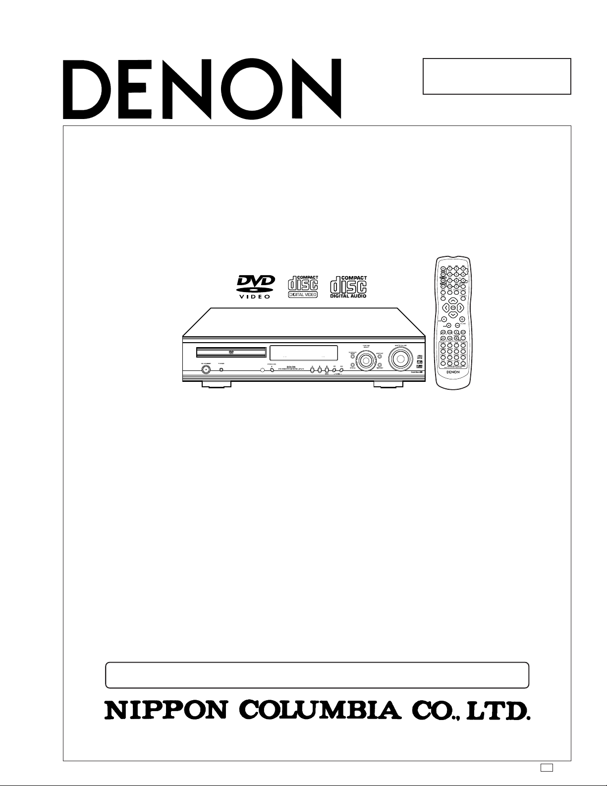
MODEL
ADV-700
DVD SURROUND RECEIVER
— TABLE OF CONTENTS —
SAFETY PRECAUTIONS ................................................... 2
SPECIFICATIONS .............................................................. 2
DIAGNOSTICS OF OPTICAL PICKUP AND
REPLACING TRAVERSE UNIT ..................................... 3~5
DISASSEMBLY ............................................................. 6~10
CAUTION IN SERVICING ................................................ 10
ELECTRICAL ADJUSTMENT .......................................... 11
BLOCK DIAGRAMS .................................................... 12,13
LEVEL DIAGRAMS ..................................................... 14,15
CLOCK FLOW ..................................................................16
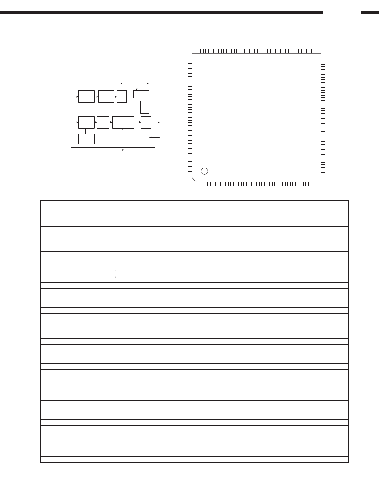
SEMICONDUCTORS ................................................ 17~46
PRINTED WIRING BOARDS .................................... 47~54
NOTE FOR PARTS LIST .................................................55
PARTS LIST OF P.W.B. UNIT .................................. 56~71
EXPLODED VIEW ............................................................. 72
PARTS LIST OF EXPLODED VIEW ................................ 73
PARTS LIST OF DVD MECHANISM UNIT ..................... 74
EXPLODED VIEW OF DVD MECHANISM ...................... 75
POINTS OF GREASING .................................................. 76
PACKING VIEW ................................................................ 77
PACKING & ACCESSORIES ........................................... 77
WIRING DIAGRAM ........................................................... 78
MEASURING METHOD AND WAVE FORMS .......... 79,80
SCHEMATIC DIAGRAMS ......................................... 81~88
(1/8) GU-3333-1 DVD MAIN UNIT (1/2) ........................... 81
(2/8) GU-3333-1 DVD MAIN UNIT (2/2) ........................... 82
(3/8) 1U-3358-1 MAIN UNIT (1/2) .................................... 83
(4/8) 1U-3358-1 MAIN UNIT (2/2) .................................... 84
1U-3358-2 REG UNIT ............................................. 84
1U-3358-3 AUDIO REG UNIT ................................. 84
1U-3358-4 PROT/FAN UNIT .................................... 84
1U-3358-5 POSISTOR UNIT ................................... 84
1U-3358-6 D-BRIDGE UNIT .................................... 84
(5/8) 1U-3359-3 VIDEO UNIT .......................................... 85
1U-3359-5 COMPONENT UNIT . .............................. 85
1U-3359-6 SCART UNIT ......................................... 85
1U-3359-7 OPT UNIT .............................................. 85
(6/8) 1U-3359-1 DISPLAY UNIT ...................................... 86
1U-3359-2 H/P UNIT ............................................... 86
1U-3359-8 SUB TRANS UNIT ................................. 86
(7/8) 1U-3360 DSP UNIT (1/2) ..................................... 87
(8/8) 1U-3360 DSP UNIT (2/2) ..................................... 88
Some illustrations using in this service manual are slightly different from the actual set.
14-14, AKASAKA 4-CHOME, MINATO-KU, TOKYO 107-8011 JAPAN
Telephone: 03 (3584) 8111
X0115 842 NC 0108
Page 2

SAFETY PRECAUTIONS
The following check should be performed for the continued protection of the customer and service technician.
LEAKAGE CURRENT CHECK
Before returning the unit to the customer, make sure you make either (1) a leakage current check or (2) a line to
chassis resistance check. If the leakage current exceeds 0.5 milliamps, or if the resistance from chassis to either
side of the power cord is less than 460 kohms, the unit is defective.
SPECIFICATIONS
Audio section
• Power amplifier
Output power: Front: 35 W + 35 W (6 Ω/ohms, 1 kHz with 10% T.H.D.)
Output terminals: Front, Center, Surrond: 6 ~16 Ω/ohms
• Analog
Input sensitivity / input impedance: 200 mV / 47 kΩ/kohms
Frequency response: 10 Hz ~ 70 kHz: +0.3 dB (DIRECT mode)
S / N : 98 dB (DIRECT mode)
Rated output: 1.2 V (Subwoofer preout, 20 Hz)
• Digital
Digital input / output: Format Digital audio interface
Video secion
• Standard video jacks
Input / output level and inpedance: 1 Vp-p, 75 Ω/ohms
• S-video jacks
Input / output level and inpedance: Y (brightness) signal 1 Vp-p, 75 Ω/ohms
• Color cimponent video jacks (DVD output) (U.S.A. & Canada model)
Input / output level and inpedance: Y (brightness) signal 1 Vp-p, 75 Ω/ohms
• AV1 connector (Europe model)
Video output: 1Vp-p, 75Ω/ohms
S-video output: Y (brightness) signal 1 Vp-p, 75 Ω/ohms
RGB output (DVD only): R/G/B signal 0.7 Vp-p, 75 Ω/ohms
Audio output: L/R (Fixed output)
Tuner section
Receiving Range
U.S.A. & Canada model: 87.50 MHz~107.90 MHz 520 MHz~1710 MHz
Europe model: 87.50 MHz~108.00 MHz 522 MHz~1611 MHz
Usable Sensitivity: 1.5 µV (14.8 dBf)
DVD section
Signal Format: NTSC/PAL
Applicable discs: (1) DVD-Video discs
Audio output: Fixed output level: 2 Vrms, (CDR/TYPE, VCR OUT)
Clock, Timer section
Clock system: Power source synchronous system
Timer functions: Everyday timer (DVD or Tuner): 1 setting
General
Power Supply: AC 120 V, 60 Hz (For U.S.A. & Canada model)
Power Consumption: 135 W (Standby 1.2 W) (For U.S.A. & Canada model)
Maximuim external
Dimensions: 434(W) × 90 (H) × 415 (D) mm (17.1” × 3.5” × 16.3”)
Mass: 9.4 kg (20.7 lbs)
Remote Control Unit RC-902 (For U.S.A. & Canada model)
Type: Infrared pulse
Power Supply: DC 3V, 2 “AA/R6P” batteries
Center: 35 W + 35 W (6 Ω/ohms, 1 kHz with 10% T.H.D.)
Surround: 35 W + 35 W (6 Ω/ohms, 1 kHz with 10% T.H.D.)
C (color) signal 0.286 Vp-p, 75 Ω/ohms (U.S.A. & Canada model)
C (color) signal 0.3 Vp-p, 75 Ω/ohms (Europe model)
B (blue) signal 0.648 Vp-p, 75 Ω/ohms
C
CR (red) signal 0.648 Vp-p, 75 Ω/ohms
C (color) signal 0.3 Vp-p, 75 Ω/ohms
[FM] (note: µV at 75 Ω/ohms, 0 dBf=1×10
1-layer 12 cm single-sided discs, 2-layer 12 cm single-sided
discs, 2-layer 12cm double-sided discs (1 layer per side)
1-layer 8 cm single-sided discs, 2-layer 8 cm single-sided
discs, 2-layer 8 cm double-sided discs (1 layer per side)
(2) Compact discs (CD-DA, Video CD)
12 cm discs, 8 cm discs
Sleep timer: maximum 120 min.
AC 230 V, 50 Hz (For Europe model)
145 W (Standby 1.2 W) (For Europe model)
RC-901 (For Europe model)
-15
W) [AM]
ADV-700
This product incorporates copyright protection technology that is protected by method claims of certain U.S. patents and other intellectual property rights
owned by Macrovision Corporation and other rights owners. Use of this copyright portection technology must be authorized by Macrovision Corporation,
and is intended for home and other limited viewing uses only unless otherwise authorized by Macrovision Corporation. Reverse engineering or
disassembly is prohibited.
∗ Design and specifications are subject to change without notice in the course of porduct improvement.
2
Page 3
ADV-700
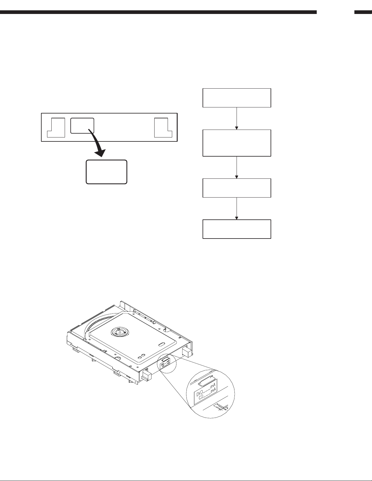
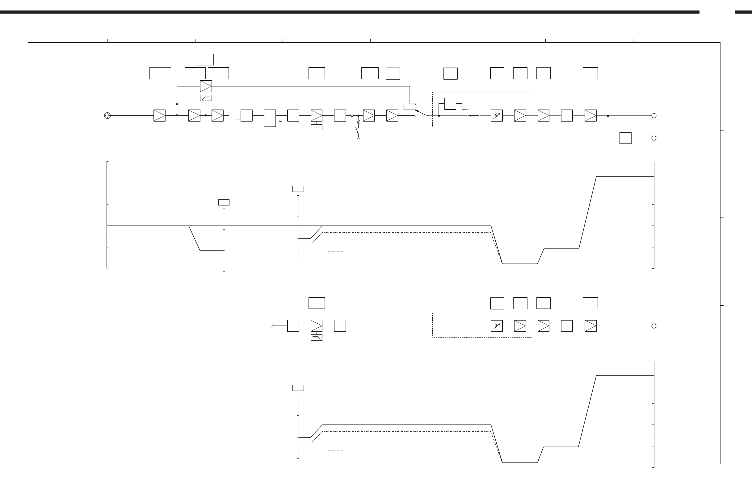
DIAGNOSTICS OF OPTICAL PICKUP AND REPLACING TRAVERSE UNIT
Make failure diagnostics of the Optical Pickup as follows.
If the laser drive current becomes more than 1.5 times of the initial value, the Optical Pickup should be replaced.
The laser drive current is registered on the seal attached to the rear of the Mecha. Unit.
In case of replacing the Pickup, change the whole part of the Traverse Unit.
No mechanical adjustment is necessary after the replacement.
Disc no read,
unsteady playback, etc.
Laser drive current check
HF wave form check
(Refer to page 79, 80)
Example:
DVD 30mA
CD 30mA
Label Indication of DVD Mechanism
Present value exceeds
the initial value by 1.5 times
Traverse Unit replacing
(See page 9 for details)
Laser current registering
after replacement
Step: Disc playback
Write the measured value
on the seal attached to the Mecha. Unit
* As to the measuring method, refer to page 4
Laser current consumption value
ex) DVD ***mA, CD ***mA
3
Page 4
ADV-700
Note for Handling the Laser Pick-up
The protection for the damage of laser diode.
If you want to change the optical device unit from any other units, you must keep the following.
(1) It should be done at the desk already took measures the static electricity in care of removing the OPU's
(Optical device unit) connector cable.
(2) Workers should be put on the "Earth Band".
(3) It shold be done to add the solder to the short land to prevent the broken Laser diode before removing the
24P FFC cable.
(4) Don't touch OPU's connector parts carelessly.
Replacement of the Laser Pick-up (Traverse Unit)
Check the Iop (Laser drive current).
If the present Iop (current) value exceeds +50% of the initial value, replace the Traverse unit (Laser Pick-up) with a new
one.
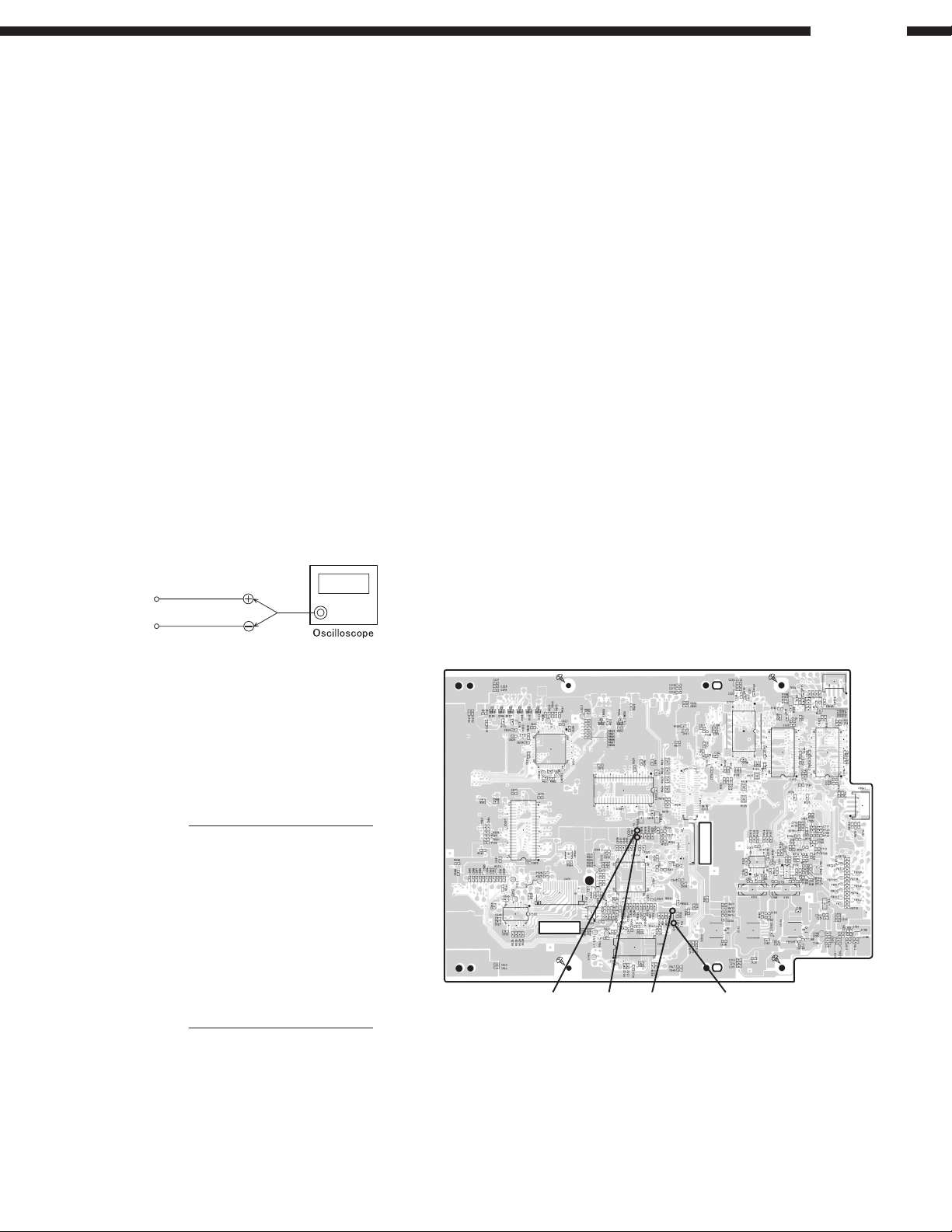
Iop Measurement Method
When measureing Laser drive current (Iop), playback the discs (CD, DVD) described below, measure Iop for CD Laser and
DVD Laser by the test point (LD1 ~ LD4) on the DVD Main P.W.B.
Test Disc : DVD/DVDT-S01 or commercially available discs.
: CD/TCD-784 (manufactured by ALMEDIO INC) or commercially available discs.
1. DVD Laser current measurement
LD2
LD1
(1) Connect the oscilloscope to LD1 of test point
for GND side and LD2 of test point for signal
side.
(2) Playback the title 1 / chapter 1 of the DVD
Test Disc.
(3) Measure the voltage between LD1 and LD2,
calculate Iop by the formula as shown below.
Measurement Voltage Value
Iop=
2. CD Laser current measurement
(1) Connect the oscilloscope to LD3 of test point
for GND side and LD4 of test point for signal
side.
(2) Playback the track 1 of the CD Test Disc.
(3) Measure the voltage between LD3 and LD4,
calculate Iop by the formula as shown below.
Iop=
39 (Resistance Value)
Measurement Voltage Value
39 (Resistance Value)
LD1LD3LD4
DVD Main Unit foil side
LD2
4
Page 5
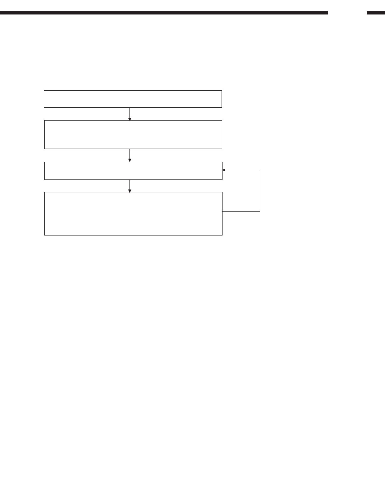
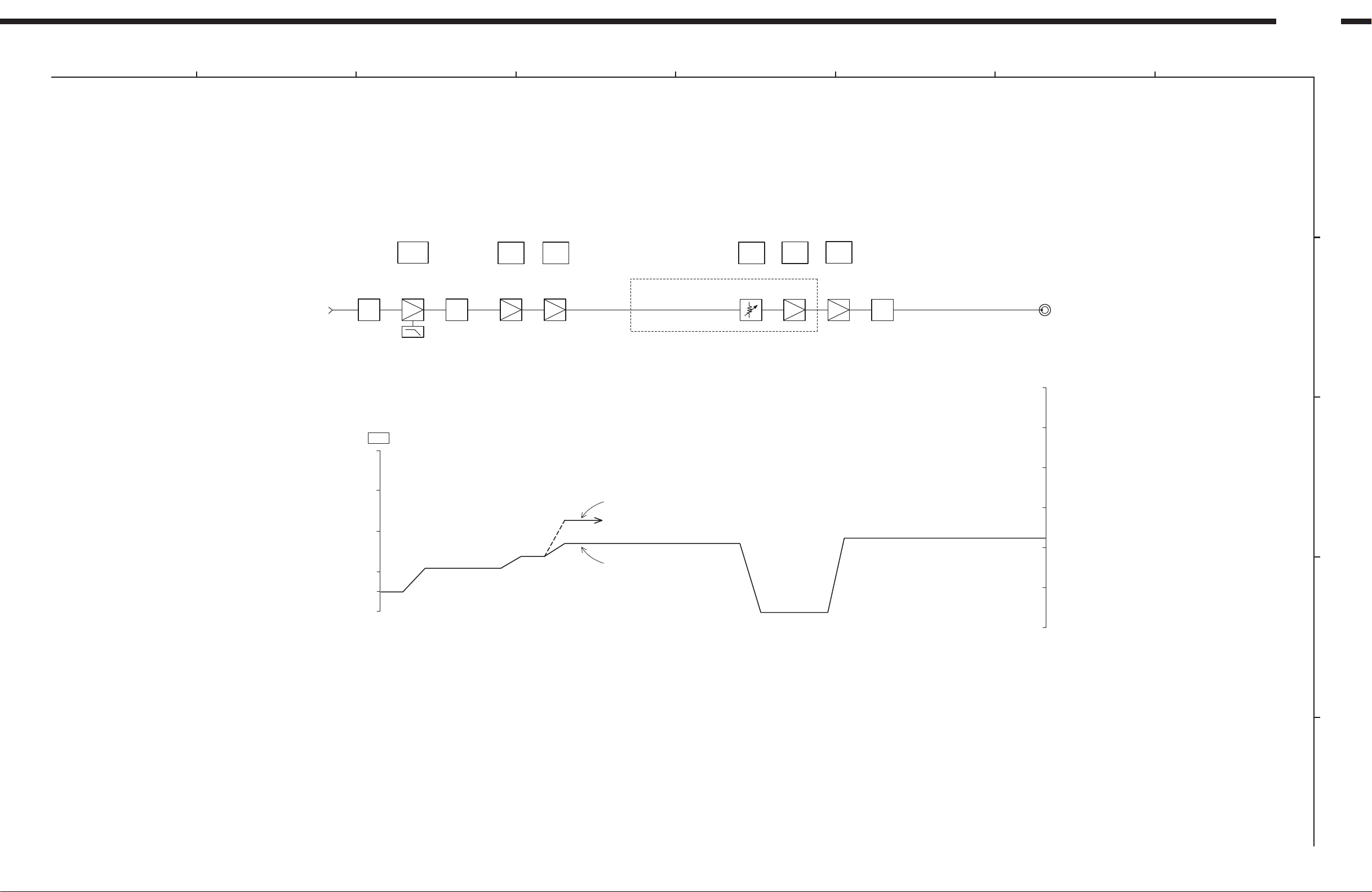
Optical Pick-up Diagnostics and Replacement
NO DISC indicated, Playback not smooth, etc.
Laser drive current check
HF signal check
Traverse Unit replacement (refer to page 9)
Present value: 50% up to initial value
Laser drive current check after replacement.
If the present value is less than 80mA, write on
the new label by hand, put on the new label over
the old label.
If the present value exceeds 80mA,
replace the Traverse Unit with a new one.
Cause: Damaged electrostatically when replaced.
When repairing, carry out failure diagnostics by following the procedure described below.
If the present value of the laser drive current is 50% up to initial value, it is the point of the pickup replacement.
In case of the pickup replacement, replace the Traverse Unit with no adjustment.
The initial value is indicated on the label on back side of Mecha.
ADV-700
5
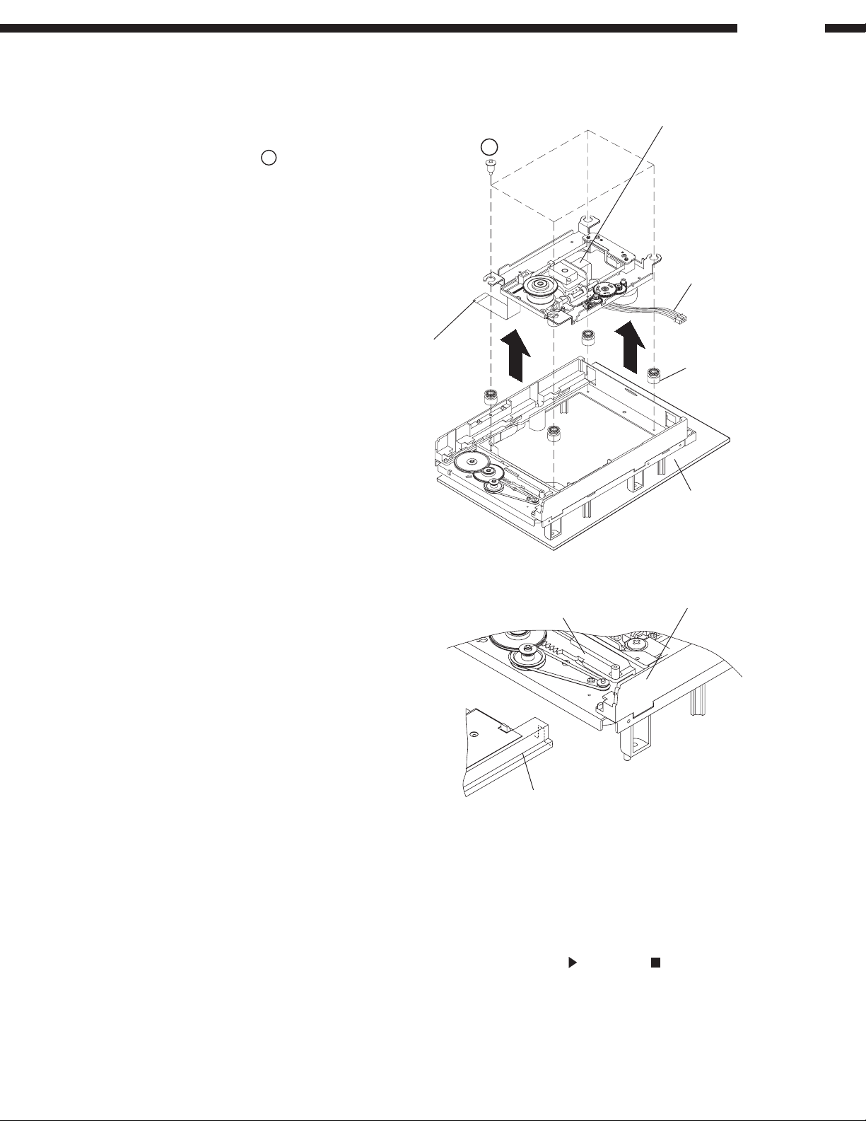
Page 6
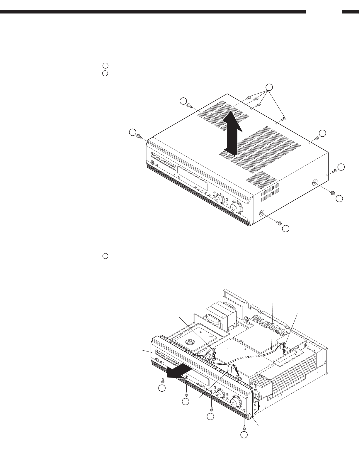
DISASSEMBLY
3
( Follow the procedure below in reverse order when reassembling )
1. Top Cover
1) Remove 4 screws 1 on both sides.
2
2) Remove 6 screws
3) Detach the Cover as shown in the arrow
direction.
on the rear panel.
1
ADV-700
2
1
2. Front Panel
1) Remove 4 screws 3 from the bottom edge of the
Front Panel.
2) Disconnect FFC, 3P Connector, and 5P Connector
from the Main PWB.
3) Detach the Front Panel together with the Inner
Panel as shown in the arrow direction.
2
2
1
1
MAIN P.W.B.
5P Connector
Front Panel
3
FFC
3
Inner Panel
3
3P Connector
6
Page 7
ADV-700
7
3. DSP PWB
1) Remove 4 screws 4 fixing the DSP PWB.
2) Disconnect FFC x 3 from the DSP PWB.
4. DVD Mecha. Unit
1) Remove 4 screws 5 on the DVD Mecha. Unit.
2) Disconnect FFC x 2, 14P Connector, and 9P
Connector from the DVD Mecha. Unit.
4
4
FFC
DSP P.W.B.
14P Connector
5
4
4
FFC
5. Rear Panel
1) Remove the Cord Bush.
2) Remove 5 screws
8
on the Rear Panel.
6
, 20 screws 7, and 3 screws
FFC
9P Connector
Cord Bush
6
8
7
6
6
7
6
7
Page 8
6. Video PWB
1) Disconnect FFC x 2, 11P Connector, and 3P
Connector from the Video PWB.
2) Detach the Video PWB from the PWB Holder.
11P Connector
(Europe Model)
10P Connector
(USA, Canada Model)
ADV-700
3P Connector
7. Main PWB
1) Remove 5 screws 9 and 1 screw 10 on the Main
PWB.
2) Remove 6 screws
Chassis.
3) Disconnect 8P, 4P x 2, and 3P Connector from the
Main PWB.
from the bottom of the
11
FFC
P.W.B. Holder
9
Video P.W.B.
FFC
Main P.W.B
9
8P Connector
10
4P
3P
11
8
Page 9
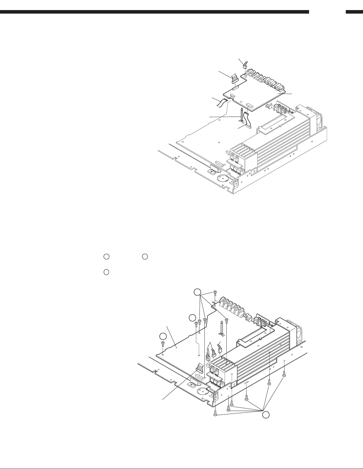
ADV-700
TRAVERSE UNIT DISASSEMBLY
(Follow the procedure below in reverse order when reassembling)
Caution: The optical pickup can be damaged easily by static electricity charged on human body. Take necessary anti-static
measures when repairing around the optical pickup.
1. Guide Clamp Bracket disassembly
(1) Remove 2 screws 1.
(2) Remove Guide Clamp Bracket to arrow direction.
2. Tray disassembly
(1) Remove to arrow direction.
(2) Solder the short-circuit (see in the frame).
1
Guide Clamp Bracket
Solder to Short-Circuit (DVD)
Solder to Short-Circuit (CD)
Tray
9
Page 10
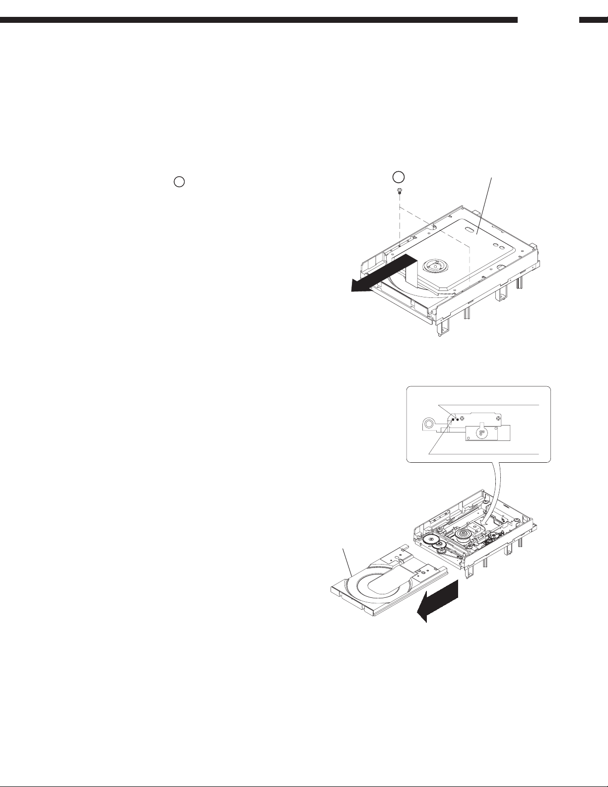
3. Traverse Unit disassembly
(1) Remove 24P FFC (CX241), 15P FFC (CX151),
5P PH WIRE (CX051) and 3P PH WIRE (CX031)
connecting with from the DVD Main P.W.B.
(2) Remove 4 screws of
(3) Remove Traverse Unit to arrow direction.
fixing Damper.
2
ADV-700
24P FFC (CX241)
2
3P PH WIRE (CX031)
15P FFC (CX151)
Damper
DVD Main P.W.B.
Note for disassembly Traverse Unit
(1) When assembling, reverse the order of the above.
(2) When inserting Tray, confirm boss on Slide Cam set
to ditch of the Tray (Compare with right drawing).
Slide gear
Tray
Boss
CAUTION IN SERVICING
Initialization
Initialization should be performed when the µcom, peripheral parts of µcom, and DVD Main P.W.B. are replaced.
How to initialize
At the player is in the state of AC OFF, turn the AC ON with pressing the PLAY ( ) and STOP ( ) buttons simultaneously.
Check that the Standby LED lights orange and the initialization has been activated. (until "INITIALIZE" disappears from
the FL display).
Note: All user settings will be lost and its factory setting will be recovered when this initialization is made. So make sure to
memorize your setting for restoring after the initialization.
10
Page 11
ADV-700
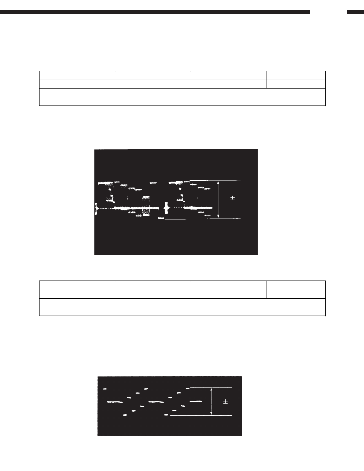
ELECTRICAL ADJUSTMENT
The following adjustment is electrical adjustments. These adjustments are to be performed after replacing the printed circuit
boards.
1. Video Output (Interlace) Adjustment
Measurement Point Adjustment Point Mode Disc
Video Output Pin Terminal VR701 Color Bar 75% T12 Playback DVD T -S01
Measuring Device: Oscilloscope 200 mV/div, 10 Ps/div
Adjustment Value: 1000 mVp-p r20 mV
For compatibility of video signal output.
1. Connect the monitor TV to the video output terminal and terminate at 75 Ohms.
2. Play back the color bar part Title 12 of the DVD Test Disc.
3. Adjust the VR701 so that the luminance signal (Y+S) output is as shown below.
Adjustment Value = 1000 mVp-p
±±
±20 mV
±±
1000mV
20mV
Luminance Signal Output
2. Video Output (Interlace) Adjustment
Measurement Point Adjustment Point Mode Disc
CB Output Pin terminal VR702 Color Bar 75% T12 Playback DVDT-SO1
Measuring Device: Oscilloscope 100 mV/div, 10 Ps/div
Adjustment Value: *525 mVp-p r11 mV Europe/Asia models
Note: CB Output should be 75 Ω terminal
For compatibility of video signal output.
1. Connect the oscilloscope to CB output Pin terminal for CH-1 and CR output Pin terminal for CH-2. (Trigger)
2. Playback the color bar part title 12 of the DVD Test Disc.
3. Adjust the VR702 so that the CB signal output is as shown below.
Adjustment Value = *525 mVp-p
±±
±11mV
±±
525mV*
*
11mV
CB Signal Output
*: 486 mVp-p
±±
±11mV for U.S.A. & Canada model
±±
11
Page 12
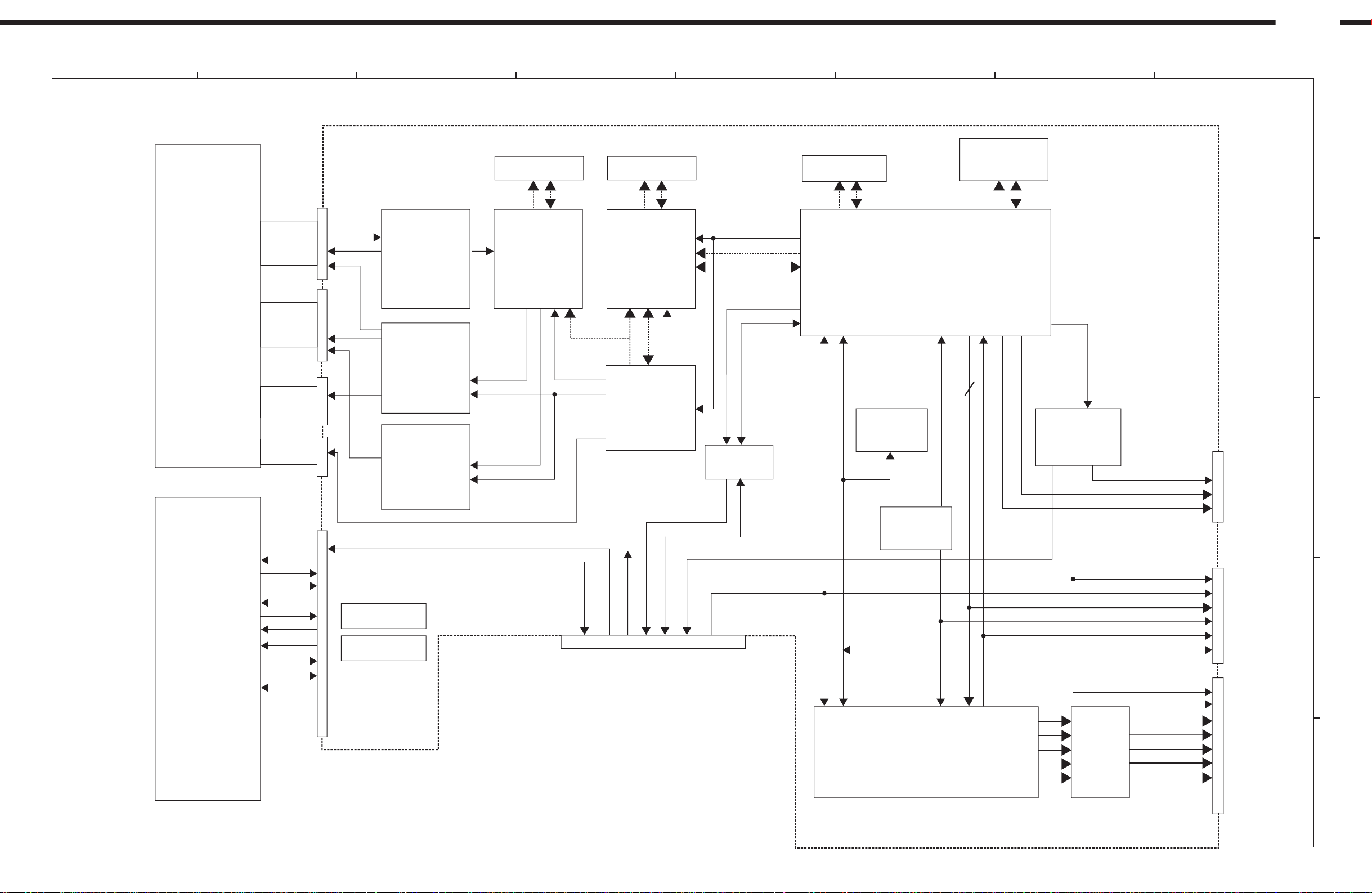
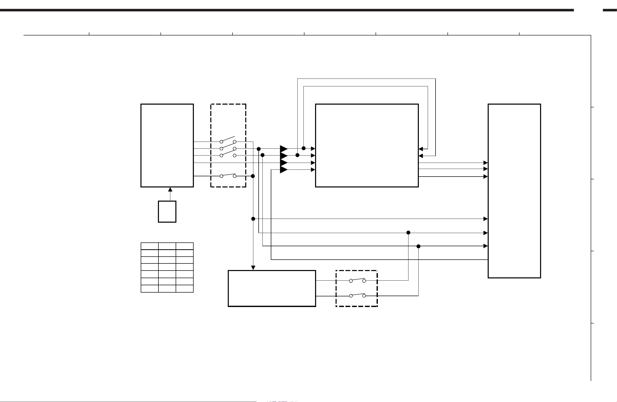
BLOCK DIAGRAMS
1
ADV-700 BLOCK DIAGRAM (1/2)
(Mechanism section)
ADV-700
2
3
4
5
76
8
DVD DRIVE
MECHA
UNIT
MAIN
UNIT
1U-3358-1
24P FFC
FFC
15P
5P P
H
3P PH
+5V[USW]
+5V[D1]
GND[D1]
+5V[V]
GND[V]
GND[A]
+12V[M]
+5V[D2]
GND[D2]
+3.7V REG.
+3.3V[D
1]REG.
FRONTE
PROCES
[TA129
4ch MO
DRIVER
[BA595
SPINDLE
MOTOR
DRIVER
[AN8471]
ND
SOR
3F]
TOR
2FP]
4M DRAM 4M DRAM
DISC SERVO
CESSOR
PRO
[TC9453F]
DMO,TRD
DMO
ON/ST
ATAPI
INTERFACE
DVD DECO
[TC946
DER
9BF]
DRIVE
-COM
m
OL
CONTR
[TMP95CW64F]
PDET
(+5V[D])
MAIN UNIT
1U-3358-1
DATA
CS,CLK
HRESET
[TC
/DFRES
7WT
/RST
125]
16M
/RST
/RST
SDRAM
2
I C BUS
x2
PROCESSOR
DVD
[ES4408]
E2PROM
[S24C01A]
27MHz
OSC
VIDEO EN
[ADV7172]
8M FLASH ROM
[HY29F080T]
8
HSYNC
VSYNC
CODER
LD8~15
I/O EXPANDER
[HCT273]
TSDO,TWS,TBCK
SPDIF
BUFFER
AMP
96k,DEEM,/DFRE
,MCLK
PROG/INT
/RST
YVU0~7
27M
HSYNC,VSYNC
SDA,SCL
VIDCNTL1,2,RGB-H
+5V[V]
G/Y
B/Cb
R/Cr
Y
C
A
B
S
DSP PWB UNIT
1U-3360
C
D
VIDEO PWB UNIT
1U-3359-3
DVD MAIN UNIT GU-3333
E
12
Page 13
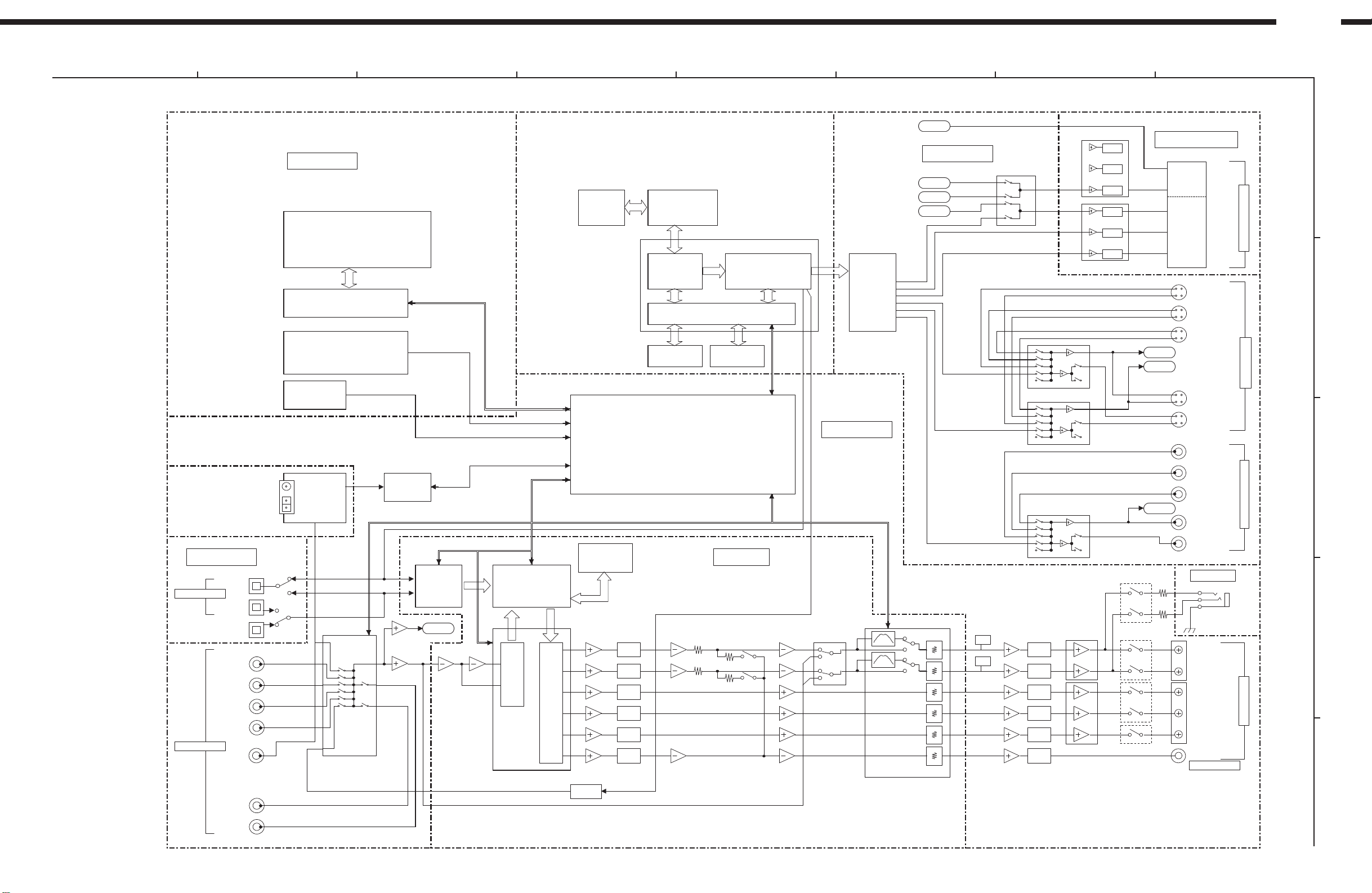
ADV-700
1
2
3
4
5
76
8
ADV-700 BLOCK DIAGRAM (2/2)
(E2 ONLY)
BA7660(Europe model only)
MUTE
MUTE
MUTE
MUTE
MUTE
MUTE
BA7660(Europe model only)
1U-3359-5,6
Europe model:SCART TERMINAL
USA,Canada model:3P PINJACK
C
C
Y
V.AUX IN
C
Y
C
Y
MONITOR OUT
C
Y
VCR OUT
C
VCR IN
A
COMPONENT VIDEO
B
S-VIDEO
1U-3359-1
FL TUBE
15-ST-36GN
FL DRIVER Y
M66005FP
KEY
ROTARY ENCODER
REMOCON
RPM6938-V4
UADV-7 (DVD ENGINE )
DVD MECHA FRONT-END CIRCUIT
DVD DECODER
ROM
CPU
M30624FGGP
CPU
RAM
ES4408
DVD DSP
VIDEO FILTER
(DOWN MIX)
1U-3358-1
ML6427
A
1U-3359-3
V
Y
C
Cr
Cb Y
Y VCR IN
C Y
V TV/DBS IN
BA4053(E2 ONLY)
BA7625
BA7626
(E2/E3 ONLY)
TUNER PACK
1U-3359-7 1U-3360
DIGITAL IN/OUT
AUDIO IN/OUT
OPT OUT DIR AUDIO DSP
OPT IN 1
OPT IN 2 SWITCHING POWER AMP
VCR IN
TV/DBS IN
V.AUX IN
CDR/TAPE IN
TUNER IN FUNCTION
(J ONLY)
VCR OUT
TC9164AN
RDS
LC72720NM
(Europe model only)
BA15218
LC89055W CS49392
A
BA15218
A/D CONVERTER
CODEC
AK4527
ROM
2Mbit
BA15218 BA15218 BA15218 LC4966 BA15218 STK402-050
MUTE
MUTE
MUTE
MUTE
6ch D/A CONVERTER
DAC
MUTE
MUTE
AD1854KRSRL
VOLUME
M62446FP
SDB
SDB
MUTE
MUTE
MUTE
MUTE
MUTE
MUTE
BA7625
STK402-250
RELAY
PIC-212DM
TV/DBS IN
C
V.AUX IN
V
MONITOR OUT
VCR OUT
COMPOSITE VIDEO
1U-3359-2
H/P
D
FRONT L
FRONT R
SURR L
SURR L
CENTER
SUBWOOFER
PREOUT
SPEAKER OUT
E
CDR/TAPE OUT
13
Page 14
LEVEL DIAGRAMS
1
ADV-700
2
3
4
5
76
8
FRONT
CD IN
(200mV) 0
(dB)
30
20
10
-10
-20
CD IN
INPUT
BUFF.AMP
+
STEREO
H.P.F.
A/D IN
REV. AMP
+
− −
-11.5dB
A/D IN
REV. AMP
fc=80Hz.12dB/OCT
A/D
0dBPS
-10dBPS
-20dBPS
-30dBPS
A/D
DSP
D/A
other ch
0dBFS
-10dBFS
-20dBFS
(106mV)
-30dBFS
D/A
D/A OUT
L.P.F.
+
6dB
SW
MIX AMP
MUTING
config1:OFF
config2:ON
− −
FROM SWch
Other than PROLOGIC
PROLOGIC
REV.
AMP
TONE
TONE
-15dB
E.VOL
-18dB
BUFF.
AMP
M62446 (1/3)
PRE.
AMP
+ +
MUTING
POWER
AMP
6.3dB
30.1dB
AT T
FRONT
SP OUT
H/P OUT
SP OUT
1.66V
(0.35W/8Ω)
A
B
C
CENTER
SURROUND
FROM
DSP
D/A
0dBFS
-10dBFS
-20dBFS
(106mV)
-30dBFS
D/A
D/A OUT
L.P.F.
+
6dB
MUTING
Other than PROLOGIC
PROLOGIC
-15dB
E.VOL
-18dB
BUFF.
AMP
M62446 (2/3)
PRE.
AMP
+ +
MUTING
POWER
AMP
6.9dB
CENTER
SURROUND
SP OUT
D
SP OUT
1.66V
(0.35W/8Ω)
30.1dB
E
14
Page 15
ADV-700
1
2
3
4
5
76
8
SUBWOOFER
A
FROM
DSP
D/A
D/A OUT
L.P.F.
+
MUTING
LINE
AMP
− −
LINE
AMP
E.VOL
BUFF.
AMP
M62446 (3/3)
PRE.
AMP
+
MUTING
SW
PREOUT
B
0dBFS
-10dBFS
-20dBFS
-30dBFS
-35dBFS
-40dBFS
D/A
6dB
2.9dB
7.5dB
3.3dB
Config-2
To FRONT ch
Config-1
-18dB
C
Subwoofer
PREOUT
75mV
18.6dB
D
E
15
Page 16
CLOCK FLOW
1
ADV-700
2
3
4
5
76
8
A
A/D SWitch
IC113
DIR DSP CODEC
IC107 IC109 IC108
LC89055W
SN74HC244
CS49329 AK4527VQ
CKOUT(13) MCLK(44)
BCK(14) (25)SCLKN1,(28)CMPCLK SCLK(43)
LRCK(15) (26)LRCLKN1,(29)CMPREQ LRCLK(42)
(17) SW1
(15) SW2
(13) SW3
(3)
(5)
(7)
SN74LV244A
DATAO(16) (22)SDATAN1 AUDATA0(41) (6)SDTI1
XMCK(20) AUDATA2(39) (8)SDTI3
( 2) SW4
(18)
(27)CMPDAT AUDATA1(40) (7)SDTI2
X'TAL
(39)MCLK
(4)BICK
DIR IN A/D IN (5)LRCK
SW1 ON OFF
SW2 ON OFF (9)SDTO
SW3 ON OFF
SW4 OFF ON (10)
SW5 OFF ON /CK Q2(7)
( 4) SW5
SN74HC244
(16)
SW6 OFF ON
IC114 Q8(13)
( 6) SW6
(14)
SN74LV4040APW
BINARY COUNTER
B
C
D
E
16
Page 17
SEMICONDUCTORS
IC's
Note: Abbreviation ahead of IC No. indicates the name of P.W.B.
DVD: DVD Main P.W.B.
MA: Main P.W.B.
D/V: Display / Video P.W.B.
DS: DSP P.W.B.
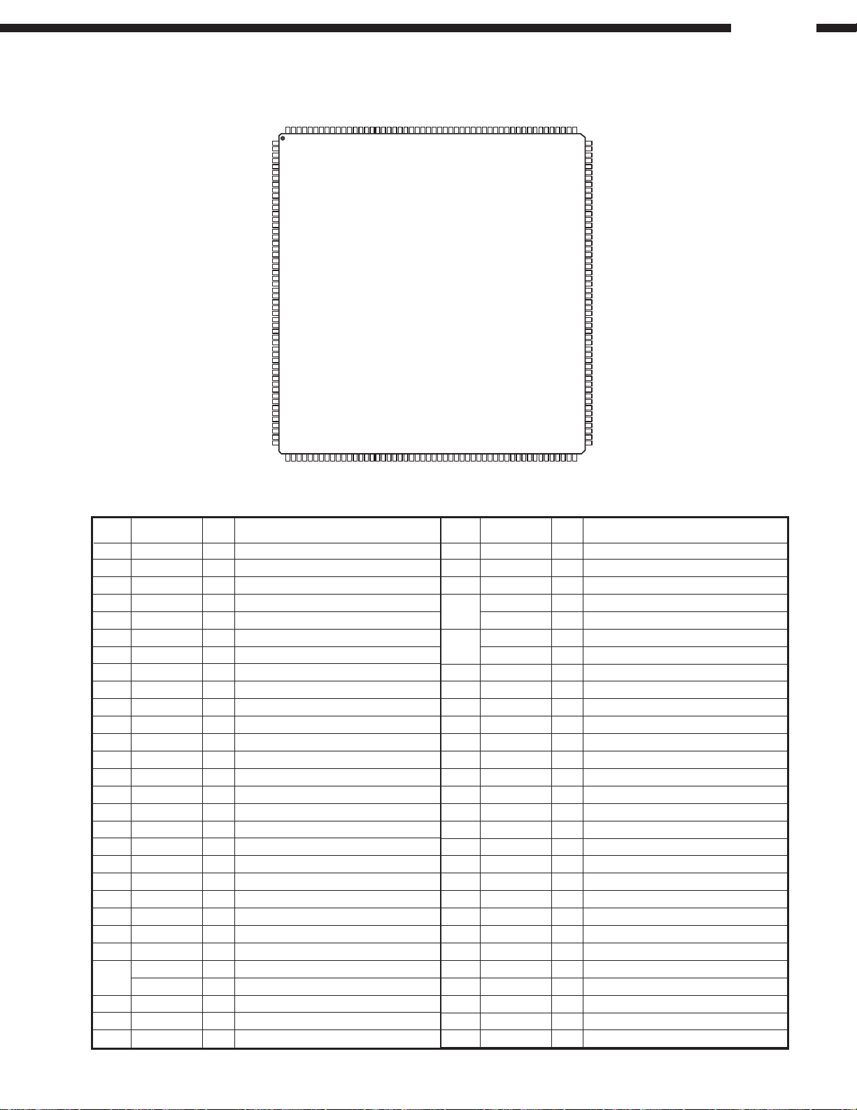
M30624FG (MA: IC101)
P9
P9
6
/ANEX1/S
P9
5
P12/D
P1
P1
P0
P0
P0
P0
P0
P0
P0
P0
7
/AN7/KI
P10
6
/AN6/KI
P10
5
/AN5/KI
P10
4
/AN4/KI
P10
3
/AN
P10
P10
2
/AN
1
/AN
P10
AV
P10
0
/AN
V
AV
7
/AD
TRG/SIN
OUT
/ANEX0/SLK4
3
/INT
11
12
13
/D
/D
/D
3
4
5
P1
P1
P1
75
74
10
2/D9
0/D8
7/D7
6/D6
5/D5
4/D4
3/D3
2/D2
1/D1
0/D0
76
77
78
79
80
81
82
83
84
85
86
3
87
2
88
1
89
0
90
3
91
2
92
1
93
SS
94
0
95
REF
96
CC
97
4
98
4
99
73
100
1
2
3
)
)
0
4
/INT
14
/D
6
P1
72
4
1
5
/-)
/D
/D
0
1
2
/INT
(/D
(/D
(/D
15
0
1
2
/D
/A
/A
/A
7
0
1
2
P2
P2
P2
P1
71
70
69
68
5
6
7
8
ADV-700
)
)
)
)
2
/D
3
(/D
3
/A
3
P2
67
9
)
3
4
5
6
)
/D
/D
4
5
(/D
(/D
4
5
/A
/A
4
5
P2
P2
66
65
10
11
7
/D
/D
6
7
(/D
(/D
(/-/D
6
7
8
9
10
11
12
13
14
15
16
/A
/A
/A
/A
/A
/A
/A
6
7
0
1
SS
CC
P2
V
P3
P2
64
12
V
P3
63
62
61
60
59
13
14
15
16
17
/A
2
3
4
5
P3
P3
P3
P3
58
57
56
55
18
19
20
21
17
/A
/A
/A
/A
6
7
0
1
P3
P3
P4
P4
54
53
52
51
50
49
48
47
46
45
44
43
42
41
40
39
38
37
36
35
34
33
32
31
30
29
28
27
26
22
23
24
25
2/A18
P4
3/A19
P4
P4
4
/CS0
P4
5
/CS1
P4
6
/CS2
7
/CS3
P4
0
/WRL/WR
P5
1
/WRH/BHE
P5
2
/RD
P5
3
/BCLK
P5
4
/HLDA
P5
5
/HOLD
P5
6
/ALE
P5
7
/RDY/CLK
OUT
P5
0
/CTS0/RTS
0
P6
1
/CLK
0
P6
P6
2
/RXD
0
3
/TXD
0
P6
P6
4
/CTS1/RTS1/CTS0/CLKS
P6
5
/CLK
1
P6
6
/RXD
1
P6
7
/TXD
1
P7
0
/RXD2/SDA/TA0
P7
1
/RXD2/SCL/TA0IN/TB5
P7
2
/CLK2/TA1
OUT
1
OUT
IN
/V
2
1
/NMI
5
P8
0
IN
/U
/U
IN
/INT
4
P8
out
/INT
/INT
3
2
/TA3
7
/TA4
P8
P8
/TA4
1
P7
0
P8
P8
/V
/W
/W
OUT
IN
IN
out
/TA3
/TA1
6
/TA2
2
/TA2
5
4
P7
P7
P7
/RTS
2
/CTS
3
7
M30624FG Terminal Function
Pin
No.
Port Name Function
Symbol
IN
/TB4
1
/DA
4
P9
IN
/TB3
0
/DA
3
P9
3
OUT
/S
IN
/TB2
4
P9
3
IN
/S
IN
/TB1
1
P9
/CLK3
IN
/TB0
0
P9
BYTE
SS
CNV
IN
SS
CIN
COUT
/X
7
/X
6
RESET
P8
P8
CC
X
OUT
V
V
X
1 P94 E2P CS Chip select signal to EEPROM
2 P93 62446 LATCH Serial data latch to E. VR IC
3 P92 62446 DATA, E2P DI, FUNC DA Serial data to EEPROM/E. VR IC/Input Switch IC
4 P91 E2P DO Serial data from EEPROM
5 P90 62446 CLK, E2P SK, FUNC CLK Serial clock to EEPROM/E. VR IC/Input Switching IC
6 BYTE (VSS) GND
7 CNVSS (PullDown), FLASH CNVss Flash write mode select input
8 P87 BUS ON/OFF Serial data/clock separate command output to E. VR IC
9 P86 FUNC CE(STB) Data latch to Input Switch IC
10 RESET RESET Reset input
11 XOUT XTAL(12.5MHz) Oscillator output (12.5 MHz)
12 VSS (VSS) GND
13 XIN XTAL(12.5MHz) Oscillator input (12.5 MHz)
14 VCC (VCC) Power supply
15 P85 (PullUp) NMI, not used
16 P84 PROTECT Speaker and Drive IC abnormal detect
17 P83 /CS Comm. chip select input with DVD
17
Page 18

ADV-700
Pin
No.
Port Name Function
18 P82 RESERVED(DENON BUS) Arbitration input on DENON BUS (same as serial data)
19 P81 50/60 Detect input of power pulse (50/60 Hz)
20 P80 FAN ON/OFF Fan motor drive output
21 P77 IN JOGB JOG pulse input B for function switching
22 P76 IN JOGA JOG pulse input A for function switching
23 P75 VOL JOGB JOG pulse input B for VOL
24 P74 VOL JOGA JOG pulse input A for VOL
25 P73 FLCS Chip select output to FL Driver IC
26 P72 RESERVED(DENON BUS) Serial sync clock output on DENON BUS
27 P71 RESERVED(DENON BUS) Serial data input on DENON BUS
28 P70 RESERVED(DENON BUS) Serial data output on DENON BUS
29 P67 FLDA, FLASH TxD Serial data output to FL Driver IC
30 P66 PULL DOWN, FLASH RxD Open pin, serial data input at flash write
31 P65 FLCK, FALSH MODE, FLASH CLK Serial clock output to FL Driver IC
32 P64 FL RESET, FLASH BUSY Reset output to FL Driver IC
33 P63 sDATAout(DVD) Serial comm. output with DVD
34 P62 sDATAin(DVD) Serial comm. input with DVD
35 P61 SCLK(DVD) Serial comm. clock input with DVD
36 P60 PWRON(DVD) Power control output for DVD unit
37 RDY/P57 /RESET Reset output to DVD unit
38 ALE/P56 H/P SW Headphone on/off detect input
39 HOLD/P55 LED G, FLASH EPM Control output to power indicator LED green
40 HLDA/P54 /DFRES Reset detect signal for DVD unit
41 BCLK/P53 DVD ON/OFF Power control output for DVD unit
42 RD/P52 RGB H Composite/S/RGB switching, aspect ratio switching
43 WRH/BHE/P51 VCNT1/YC H Aspect ratio switching input (16:9, 4:3LB, 4:3)
44 WRL/WR/P50 LED R, FLASH CE Control output to power indicator LED red
45 CS3/P47 VCNT2/WIDE Aspect ratio switching input (16:9, 4:3LB, 4:3), WIDE
46 CS2/P46 DSEL1 Digital in/out select output
47 CS1/P45 S-SEL Select output of monitor source internal/external
48 CS0/P44 A Select output A of external input source
49 A19/P43 B Select output B of external input source
50 A18/P42 C Select output C of external input source
51 A17/P41 SCART MUTE Mute output of SCART pin
52 A16/P40 TEMP Temp. sensor input
53 A15/P37 DSEL2 Open
54 A14/P36 SDB ON/OFF SDB ON/OFF output
55 A13/P35 FRT MUTE(VR MUTE) Mute output of all channel (mute output of front channel)
56 A12/P34 SW MUTE Mute output of sub-woofer channel
57 A11/P33 RL FRONT Speaker relay ON/OFF output of front channel
58 A10/P32 RL SURR Speaker relay ON/OFF output of surround channel
59 A9/P31 RL CENT Speaker relay ON/OFF output of center channel
60 VCC (VCC) Power supply
61 A8/P30 RL HP Headphone relay ON/OFF output
62 VSS (VSS) GND
63 A7/P27 OPEN Open
64 A6/P26 STEREO Tuner’s stereo indicator input
65 A5/P25 TUNED Tuner’s station detect input
66 A4/P24 T.MUTE Tuner’s mute output
67 A3/P23 SANYO CE Comm. chip enable output to PLL/RDS IC of tuner
68 A2/P22 SANYO DI Serial data output to PLL/RDS IC of tuner
69 A1/P21 SANYO CLK Serial clock output to PLL/RDS IC of tuner
70 A0/P20 SANYO DO Serial data input from PLL/RDS IC of tuner
71 D15/P17 INTREQ OUT Comm. request input from surround DSP
Symbol
18
Page 19
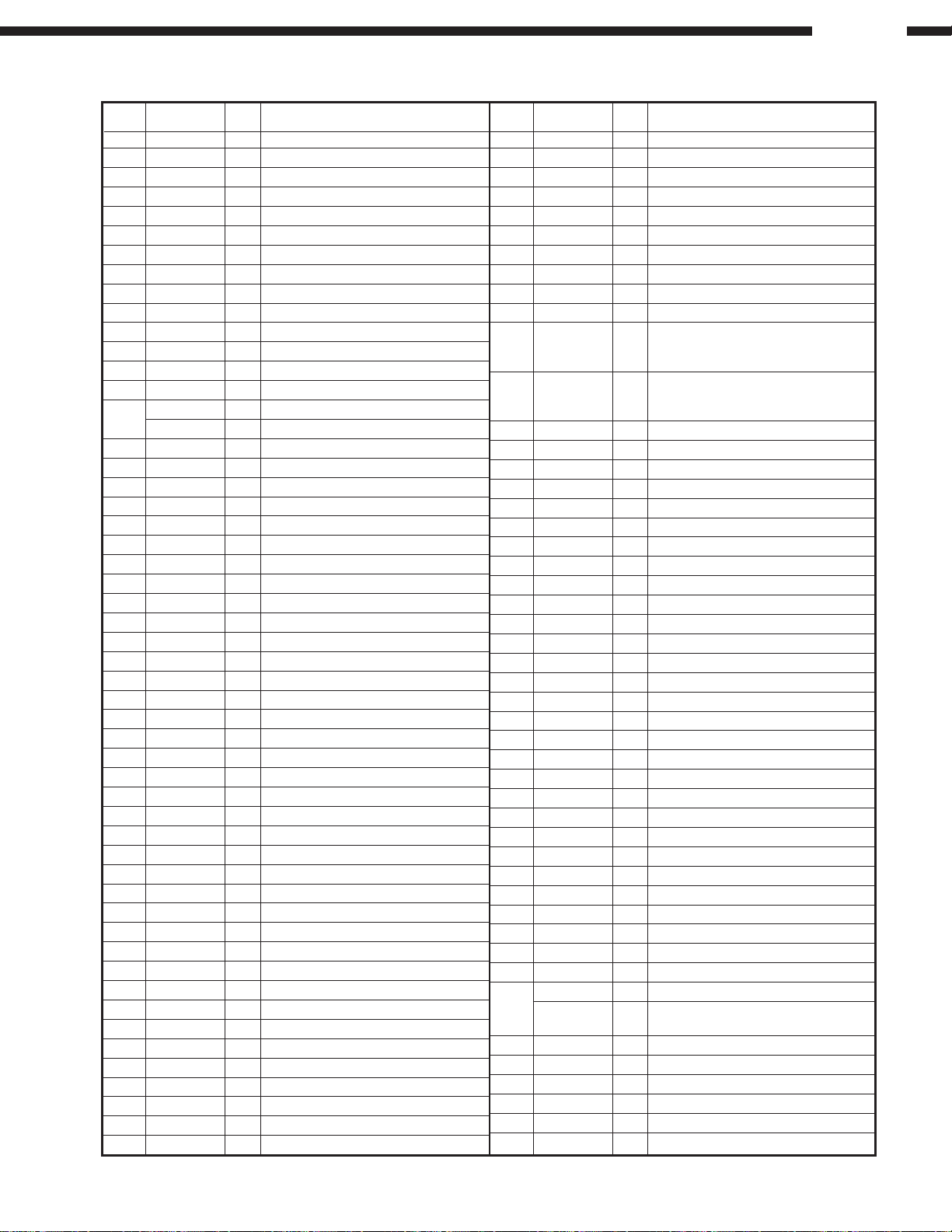
ADV-700
Pin
No.
100 P95 89055 CLK, 4527 CLK, 4932 CLK Serial clock output to DIR/CODEC/DSP
Port Name Function
72 D14/P16 89055 CSFLAG Signal change detect input from DIR
73 D13/P15 REMOTE IR remote control input
74 D12/P14 /SYR Reset output to RDS IC of tuner
75 D11/P13 INTREQ IN Open drain operation (L: output, H: switch to input)
76 D10/P12 4932 CE Serial comm. chip enable output to surround DSP
77 D9/P11 4932 RST Reset output to surround DSP
78 D8/P10 4527 CE Serial comm. chip enable output to CODEC(AD/DA)
79 D7/P07 ROM/RAM ROM/RAM used surround DSP select output
80 D6/P06 ROM2 ROM address used surround DSP select output
81 D5/P05 ROM3 ROM address used surround DSP select output
82 D4/P04 ROM30 ROM address used surround DSP select output
83 D3/P03 ERR MUTE Digital mute output when error
84 D2/P02 SEL CLK Data clock select output
85 D1/P01 4527 RST Reset output to CODEC
86 D0/P00 89055 CE Serial comm. enable output to DIR
87 P107 96 DET 96kHz sampling signal detect input from DIR
88 P106 89055 ERR Error input from DIR
89 P105 89055 RST Reset output to DIR
90 P104 P.ON/OFF Whole unit’s power ON/OFF (standby) output
91 P103 AAC AAC function on/off select input
92 P102 MODE1 Unit’s operation spec select input
93 P101 KEY 0 Button operation detect input
94 AVSS (VSS) GND
95 P100 KEY 1 Button operation detect input
96 VREF (VCC) Ref. V input for A/D conversion
97 AVCC (VCC) Power supply
98 P96 89055 DO, 4932 DO Serial data input from DIR/CODEC/DSP
99 P97 89055 DIN, 4527 DIN, 4932 DIN Serial data output to DIR/CODEC/DSP
Symbol
19
Page 20
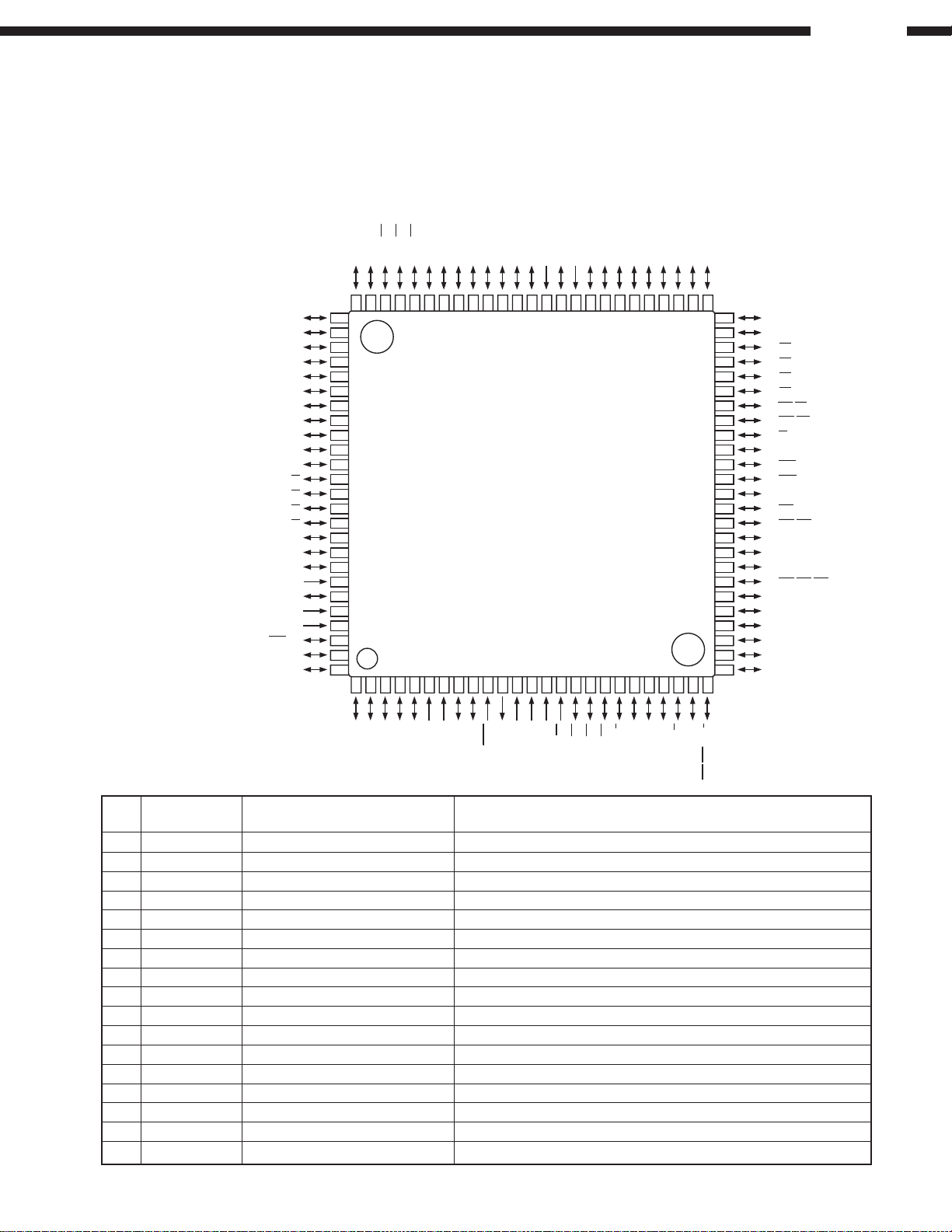
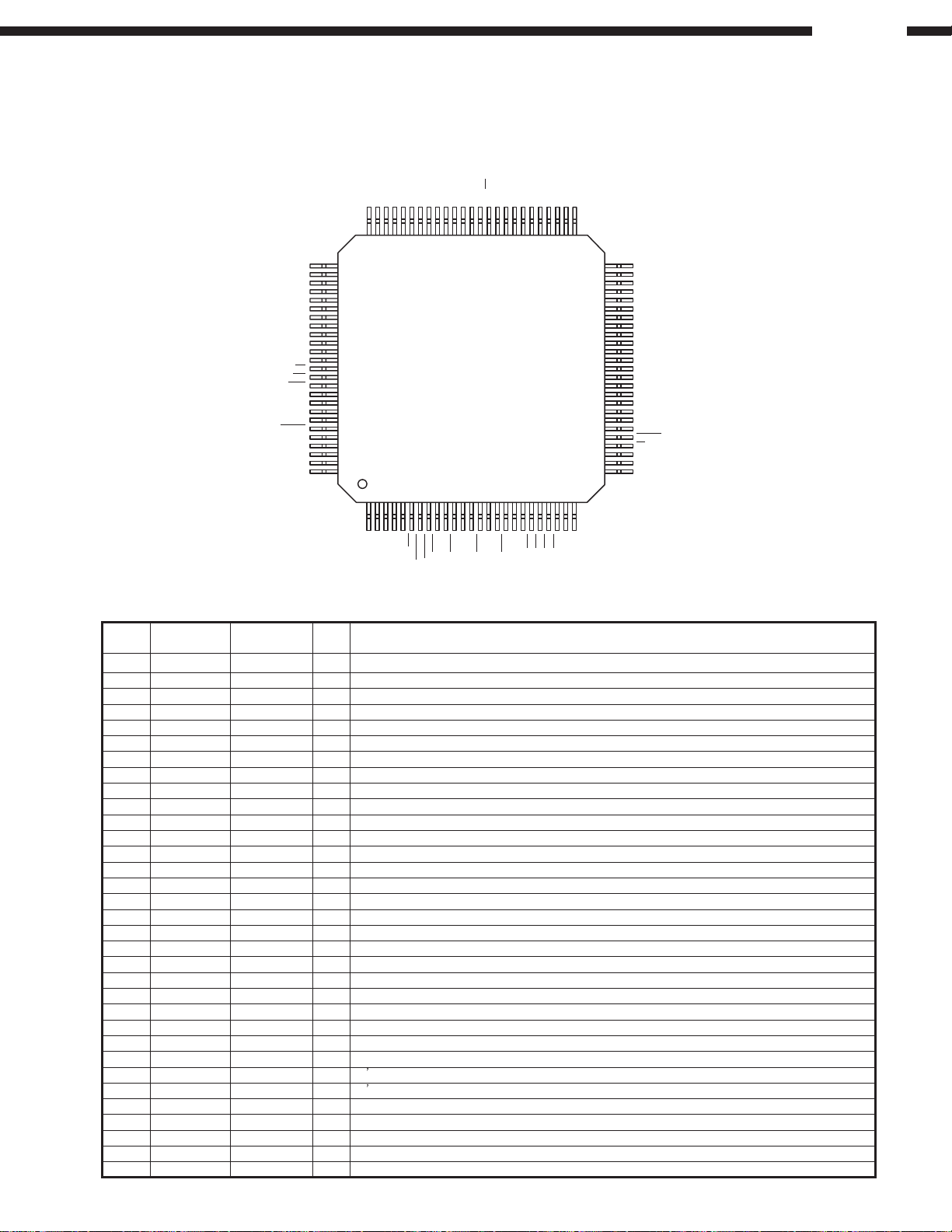
ES4408F (DVD: IC101)
Vcc
LA4
LA5
LA6
LA7
LA8
LA9
Vss
Vcc
LA10
LA11
LA12
LA13
LA14
LA15
LA16
Vss
Vcc
LA17
LA18
LA19
LA20
LA21
RESET#
TDMDX/RSEL
Vss
Vcc
TDMDR
TDMCLK
TDMFS
TDMTSC#
TWS/SEL_PLL1
TSD/SEL_PLL0
Vss
Vcc
TSD1
TSD2
TSD3
MCLK
TBCK
SPDIF_DOBM
NC
Vss
Vcc
RSD
RWS
RBCK
APLLCAP
XIN
XOUT
Vcc
Vss
ES4408F Terminal Function
Vss
LA3
LA2
LA1
LA0NCNC
Vcc
Vss
LWRHL#
LWRLL#
LD15
LD14
LD13
LD12
Vcc
Vss
LD11
LD10
LD9
LD8
LD7
LD6
LD5
Vss
Vcc
LD4
LD3
LD2
LD1
LD0
Vss
LCS3#
LCS2#
LCS1#
LCS0#
Vcc
Vss
LOE#
AUX7
AUX6
AUX5
208
207
206
205
204
203
202
201
200
199
198
197
196
195
194
193
192
191
190
189
188
187
186
185
184
183
182
181
180
179
178
177
176
175
174
173
172
171
170
169
168
1
2
3
4
5
6
7
8
9
10
11
12
13
14
15
16
17
18
19
20
21
22
23
24
25
26
27
28
29
30
31
32
33
34
35
36
37
38
39
40
41
42
43
44
45
46
47
48
49
50
51
52
5354555657585960616263646566676869707172737475767778798081828384858687888990919293949596979899
Vcc
Vss
Vss
Vcc
Vcc
Vss
Vcc
Vss
DB0
DB1
DB2
DB3
DB4
DB5
DB6
DMA0
DMA1
DMA2
DMA3
DMA4
DMA5
DMA6
DMA7
DMA8
DMA9
DWE#
DMA10
DMA11
DCAS#
DRAS0#
DRAS1#
DRAS2#
DOE#/DSCK_EN
DB7
167
Vss
Vcc
DB8
DB9
DB10
DB11
DB12
DB13
ADV-700
AUX4
AUX3
Vcc
Vss
AUX2
AUX1
AUX0
VPP
HA2
Vcc
166
165
164
163
162
161
160
159
158
157
156
Vss
155
HA1
154
HA0
153
HCS3FX#
152
HCS1FX#
151
HIOCS16#
150
HRD#/DCI_ACK#
149
HWR#/DCI_CLK
148
Vcc
147
Vss
146
HIORDY
145
HRST#
144
HIRQ/DCI_ERR#
143
HRDQ#
142
HWRQ#/DCI_REQ#
141
HD15
140
HD14
139
Vcc
138
Vss
137
HD13
136
HD12
135
HD11
134
HD10
133
HD9
132
HD8/DCI_FDS#
131
HD7/DCI7
130
Vcc
129
Vss
128
HD6/DCI6
127
HD5/DCI5
126
HD4/DCI4
125
HD3/DCI3
124
HD2/DCI2
123
HD1/DCI1
122
HD0/DCI0
121
Vcc
120
Vss
119
HSYNCH#
118
VSYNCH#
117
PCLKQSCN
116
PCLK2XSCN
115
YUV7
114
YUV6
113
YUV5
112
Vss
111
Vcc
110
YUV4
109
YUV3
108
YUV2
107
YUV1
106
YUV0
105
DCLK
100
101
102
103
104
Vss
Vcc
Vss
Vcc
DQM
DB14
DB15
DSCK
DCS1#
DCS0#
Pin No.
Pin Name
I/O
Function
1 Vcc I 3.6V power supply
2 LA 4 O Device address output
3 LA 5 O Device address output
4 LA 6 O Device address output
5 LA 7 O Device address output
6 LA 8 O Device address output
7 LA 9 O Device address output
8 Vss I GND
9 Vcc I 3.6V power supply
10 LA 10 O Device address output
11 LA 11 O Device address output
12 LA 12 O Device address output
13 LA 13 O Device address output
14 LA 14 O Device address output
15 LA 15 O Device address output
16 LA 16 O Device address output
17 Vss I GND
18 Vcc I 3.6V power supply
19 LA 17 O Device address output
20 LA 18 O Device address output
21 LA 19 O Device address output
22 LA 20 O Device address output
23 LA 21 O Device address output
24 RESET# I Reset input, active low
TDMDX O TDM transmit data
25
RSEL I ROM select
26 Vss I GND
27 Vcc I 3.6V power supply
28 TDMDR I TDM receive data
Pin Name
I/O
FunctionPin No.
29 TDMCLK I TDM clock input
30 TDMFS I TDM frame sync
31 TDMTSC# O TDM output enable, active low
TWS O Audio transmit frame sync
32
SEL_PLL1 I Select PLL1
TSD0 O Audio transmit serial data port0
33
SEL_PLL0 I Select PLL0
34 Vss I GND
35 Vcc I 3.6V power supply
36 TSD1 O Audio transmit serial data port1
37 TSD2 O Audio transmit serial data port2
38 TSD3 O Audio transmit serial data port3
39 MCLK I/O Audio master clock for audio DAC
40 TBCK I/O Audio transmit bit clock
41
SPDIF_DOBM
O S/PDIF (IEC958) format output
42 NC No connect pin
43 Vss I GND
44 Vcc I 3.6V power supply
45 RSD I Audio receive serial data
46 RWS I Audio receive frame sync
47 RBCK I Audio receive bit clock
48 APLLCAP I Analog PLL capacitor
49 XIN I Crystal input
50 XOUT O Crystal output
51 Vcc I 3.6V power supply
52 Vss I GND
53 DMA 0 O DRAM address bus
54 DMA 1 O DRAM address bus
55 DMA 2 O DRAM address bus
20
Page 21
ADV-700
Pin Name
56 DMA 3 O DRAM address bus
57 DMA 4 O DRAM address bus
58 DMA 5 O DRAM address bus
59 Vcc I 3.6V power supply
60 Vss I GND
61 DMA 6 O DRAM address bus
62 DMA 7 O DRAM address bus
63 DMA 8 O DRAM address bus
64 DMA 9 O DRAM address bus
65 DMA 10 O DRAM address bus
66 DMA 11 O DRAM address bus
67 Vss I GND
68 Vcc I 3.6V power supply
69 DCAS# O Column address strobe, active low
DOE# O Output enable, active low
70
DSCK_EN I Clock enable, active low
71 DWE# O DRAM write enable, active low
72 DRAS 0# O Row address strobe, active low
73 DRAS 1# O Row address strobe, active low
74 DRAS 2# O Row address strobe, active low
75 Vcc I 3.6V power supply
76 Vss I GND
77 DB 0 I/O DRAM data bus
78 DB 1 I/O DRAM data bus
79 DB 2 I/O DRAM data bus
80 DB 3 I/O DRAM data bus
81 DB 4 I/O DRAM data bus
82 DB 5 I/O DRAM data bus
83 Vcc I 3.6V power supply
84 Vss I GND
85 DB 6 I/O DRAM data bus
86 DB 7 I/O DRAM data bus
87 DB 8 I/O DRAM data bus
88 DB 9 I/O DRAM data bus
89 DB 10 I/O DRAM data bus
90 DB 11 I/O DRAM data bus
91 Vss I GND
92 Vcc I 3.6V power supply
93 DB 12 I/O DRAM data bus
94 DB 13 I/O DRAM data bus
95 DB 14 I/O DRAM data bus
96 DB 15 I/O DRAM data bus
97 DCS 1# O SDRAM chip select [1], active low
98 Vss I GND
99 Vcc I 3.6V power supply
100 DCS 0# O SDRAM chip select [0], active low
101 DQM O Data input/output mask
102 DSCK O Clock to SDRAM
103 Vss I GND
104 Vcc I 3.6V power supply
105 DCLK I Clock input (27MHz)
106 YUV 0 O 8-bit YUV output
107 YUV 1 O 8-bit YUV output
I/O
FunctionPin No.
Pin Name
108 YUV 2 O 8-bit YUV output
109 YUV 3 O 8-bit YUV output
110 YUV 4 O 8-bit YUV output
111 Vcc I 3.6V power supply
112 Vss I GND
113 YUV 5 O 8-bit YUV output
114 YUV 6 O 8-bit YUV output
115 YUV 7 O 8-bit YUV output
116
PCLK2XSCN
117
PCLKQSCN
118 VSYNCH# I/O
119 HSYNCH# I/O
120 Vss I GND
121 Vcc I 3.6V power supply
122 HD 0 I/O Host data bus
123 HD 1 I/O Host data bus
124 HD 2 I/O Host data bus
125 HD 3 I/O Host data bus
126 HD 4 I/O Host data bus
127 HD 5 I/O Host data bus
128 HD 6 I/O Host data bus
129 Vss I GND
130 Vcc I 3.6V power supply
131 HD 7 I/O Host data bus
132 HD 8 I/O Host data bus
133 HD 9 I/O Host data bus
134 HD 10 I/O Host data bus
135 HD 11 I/O Host data bus
136 HD 12 I/O Host data bus
137 HD 13 I/O Host data bus
138 Vss I GND
139 Vcc I 3.6V power supply
140 HD 14 I/O Host data bus
141 HD 15 I/O Host data bus
142 HWRQ# O Host write request
143 HRDQ# O Host read request
144 HIRQ I/O Host interrupt
145 HRST# O Host reset
146 HIORDY I Host I/O ready
147 Vss I GND
148 Vcc I 3.6V power supply
HWR# O Host write request
149
HWR#/DCI_ACK#
150
HRD#/DCI_CLK
151 HIOCS16# I Device 16-bit data transfer
152 HCS1FX# O Host select 1
153 HCS3FX# O Host select 3
154 HA 0 I/O Host address bus
155 HA 1 I/O Host address bus
I/O
I/O 2X pixel clock
I/O Pixel clock
Vertical sync for screen video interface,
programmable for rising or falling edge,
active low
Horizontal sync for screen video
interface, programmable for rising or
falling edge, active low
Host write / DCI interface acknowledge
I, I
signal, active low
I, I Host read / DCI interface clock
FunctionPin No.
21
Page 22
ADV-700
Pin Name
156 Vss I GND
157 Vcc I 3.6V power supply
158 HA 2 I/O Host address bus
159 VPP I Peripheral protection voltage
160 AUX 0 I/O Auxiliary port, (SDATA) I/O
161 AUX 1 I/O Auxiliary port, (SCLK) O
162 AUX 2 I/O Auxiliary port, (VFD DATA) I/O
163 Vss I GND
164 Vcc I 3.6V power supply
165 AUX 3 I/O Auxiliary port, (AMUTE) O
166 AUX 4 I/O Auxiliary port, (IR) I
167 AUX 5 I/O Auxiliary port, (POWER) I
168 AUX 6 I/O Auxiliary port, (VFDCS) O
169 AUX 7 I/O Auxiliary port, (VFDCLK) O
170 LOE# O Device output enable, active low
171 Vss I GND
172 Vcc I 3.6V power supply
173 LCS 0# O Chip select [0], active low
174 LCS 1# O Chip select [1], active low
175 LCS 2# O Chip select [2], active low
176 LCS 3# O Chip select [3], active low
177 Vss I GND
178 LD 0 I/O Device data bus
179 LD 1 I/O Device data bus
180 LD 2 I/O Device data bus
181 LD 3 I/O Device data bus
182 LD 4 I/O Device data bus
183 Vcc I 3.6V power supply
184 Vss I GND
185 LD 5 I/O Device data bus
186 LD 6 I/O Device data bus
187 LD 7 I/O Device data bus
188 LD 8 I/O Device data bus
189 LD 9 I/O Device data bus
190 LD 10 I/O Device data bus
191 LD 11 I/O Device data bus
192 Vss I GND
193 Vcc I 3.6V power supply
194 LD 12 I/O Device data bus
195 LD 13 I/O Device data bus
196 LD 14 I/O Device data bus
197 LD 15 I/O Device data bus
198 LWRLL# O Device write enable, active low
199 LWRHL# O Device write enable, active low
200 Vss I GND
201 Vcc I 3.6V power supply
202 NC No connect pin
203 NC No connect pin
204 LA 0 O Device address output
205 LA 1 O Device address output
206 LA 2 O Device address output
207 LA 3 O Device address output
208 Vss I GND
I/O
FunctionPin No.
22
Page 23
ADV-700
TC9453F (DVD: IC505)
from
RF-Amp.
(servo signal)
from
RF-Amp.
(RF signal)
ADC
RF Signal
Process
PLL
Sync
Digital
Servo
DSP
to Driver
Output
I/F
ECC
1Mbit
DRAM
Digital
IN
1bit DAC
for CD-DA
MPU I/F
Analog
Out
Clock
PLL
Output
I/F
Data Out
MPU
LPFN
LPFO
PV
VCO
VCOF
SLCO1
TESM9
TEST2
RFCD
RFDVD
RFCT
RFZ1
TEZ1
AWIN
RFSB
RFRP
TESM10
EXTAD
AWCTL
DMO
TEBC
FEBC
DPDC
EQBC
ANMON
/DFCT
VRCK
FGIN
133
134
135
REF
136
REF
137
138
DD
PV
139
140
141
142
143
144
AV
DD
145
146
147
148
149
SS
AV
150
FE1
151
TE1
152
153
154
SS
AV
155
156
157
REF
V
158
FOO
159
TRO
160
DD
AV
161
162
FMO
163
164
165
166
167
168
169
170
171
SS
3
V
SCD
172
173
SCL
174
SCB
175
176
NC
SS
PDON2
PDOP2
PDON1
PDOP1
PESP
PV
PESV
132
131
130
129
128
127
126
123456789
SS
DD
LO
NC
NC
RO
DVR
DV
DV
PPW
CFC2
CFC1
125
124
123
101112131415161718192021222324252627282930313233343536373839404142
SSXVSS
XI
XO
DV
TC9453F Terminal Function
Pin Name FunctionPin No. I/O
1NC
2NC
3DVSS GND for DAC
4 RO O R-ch output signal, Analog output pin
5DVDD Power for DAC
6 DVR O Amp ref. signal output, Analog input pin
7 LO O L-ch output signal, Analog output pin
8DVSS GND for DAC
9XVSS GND for oscillator
10 XI I X tal osc. input, Analog input pin
11 XO O X tal osc. output, Analog output pin
12 XVDD Power for oscillator
13 TESM0 Test pin, Connect to GND
14 TESM1 Test pin, Open
15 TESM2 Test pin, Connect to VDD3
16 VDD3 3.3V digital power
17 VSS3 3.3V digital GND
18 VPFC O Clock PLL block phase/freq. comparator out, Analog output pin
19 TEST0 I Test mode pin, Connect to VDD3
20 VLPFI I VCO block filter input for clock PLL, Analog input pin
21 VLPFO O VCO block filter output for clock PLL, Analog output pin
22 VSS3 3.3V digital GND
23 MON0 O Test monitor
24 MON1 O Test monitor
25 MON2 O Test monitor
26 MON3 O Test monitor
27 MON4 O Test monitor
28 MON5 O Test monitor
29 MON6 O Test monitor
30 MON7 O Test monitor
31 MON8 O Test monitor
32 MON9 O Test monitor
33 VDD3 3.3V digital power
34 NC
35 NC
36 TEST1 I Test mode pin, Connect to VDD3
37 FLGA I/O Universal I/O or flag monitor
38 FLGB I/O Universal I/O or flag monitor
39 VSS3 3.3V digital GND
40 /RST I Reset pin, Pull-up resister built-in
3
3
SS
TESM8
TESM7
TESM6
TESM5
V
122
121
120
119
118
DD
XV
TESM0
TESM1
TESM2
117
3
DD
V
PLCK
DD
V
116
115
3
SS
V
VPFC
NCNCBD15
114
113
VLPF1
TEST0
5
3
SS
SS
BD12
BD11
BD10
BD9
V
BD8
BD14
BD13
112
111
3
SS
V
VLPF0
BD7
V
110
109
108
107
106
105
104
103
MON0
MON1
MON2
MON3
MON4
MON5
MON6
MON7
MON8
BD6
BD5
BD4
BD3
BD2
BD1
9998979695949392919089
102
101
100
3
DD
NC
NC
V
FLGA
MON9
TEST1
5
3
DD
DD
BD0
V
/BWU
/BWL
/BCAS
/BRAS
/BOE
V
BA8
88
BA7
87
BA6
86
BA5
85
BA4
84
V
SS
5
83
BA3
82
BA2
81
BA1
80
BA0
79
DD
3
V
78
TESM4
77
DIGI
76
TESM3
75
DD
5
V
74
PDCK
73
/PDRQ
72
/PSYC
71
PD8
70
PD7
69
PD6
68
PD5
67
SS
3
V
66
PD4
65
PD3
64
PD2
63
PD1
62
SS
5
V
61
PD0
60
V
DD
3
59
VMCK
58
SMCK
57
NC
56
NC
55
DD
5
V
54
MD7
53
MD6
52
MD5
51
MD4
50
MD3
49
MD2
48
MD1
47
MD0
46
45
/MINT
43
44
3
SS
/MA
V
/RST
/MCE
/MRD
FLGB
/MWR
23
Page 24

Pin Name FunctionPin No. I/O
41 /MA I µcom address enable signal, Fail-safe pin
42 /MRD I µcom data read signal, Fail-safe pin
43 /MWR I µcom data write signal, Fail-safe pin
44 /MCE I µcom chip enable signal, Fail-safe pin
45 /MINT O µcom interrupt signal, Open drain pin
46 MD0 O µcom data bus
47 MD1 O µcom data bus
48 MD2 O µcom data bus
49 MD3 O µcom data bus
50 MD4 O µcom data bus
51 MD5 O µcom data bus
52 MD6 O µcom data bus
53 MD7 O µcom data bus
54 VDD5 Power for 5V
55 NC
56 NC
57 SMCK O 22M block clock output
58 VMCK O Data output block (signal processing system) clock output
59 VDD3 3.3V digital power
60 PD0 O DVD/CD data output
61 VSS5 GND for 5V
62 PD1 O DVD/CD data output
63 PD2 O DVD/CD data output
64 PD3 O DVD/CD data output
65 PD4 O DVD/CD data output
66 VSS3 3.3V digital GND
67 PD5 O DVD/CD data output
68 PD6 O DVD/CD data output
69 PD7 O DVD/CD data output
70 PD8 O DVD/CD data output
71 /PSYC O DVD data sector sync signal
72 /PDRQ O DVD data transfer block
73 PDCK O DVD data transfer clock
74 VDD5 Power for 5V
75 TESM3 Test pin, Connect to VSS5
76 DIGI I 1bit DAC digital-in input
77 TESM4 Test pin, Connect to VSS5
78 VDD3 3.3V digital power
79 BA0 O External RAM address output
80 BA1 O External RAM address output
81 BA2 O External RAM address output
82 BA3 O External RAM address output
83 VSS5 GND for 5V
84 BA4 O External RAM address output
85 BA5 O External RAM address output
86 BA6 O External RAM address output
87 BA7 O External RAM address output
88 BA8 O External RAM address output
89 VDD3 3.3V digital power
90 /BOE O External RAM/OE signal
91 /BRAS O External RAM/RAS signal
92 /BCAS O External RAM/CAS signal
93 /BWL O External RAM Lower/WE signal
94 /BWU O External RAM Upper/WE signal
95 VDD5 Power for 5V
96 BD0 I/O External RAM data in/output
97 BD1 I/O External RAM data in/output
98 BD2 I/O External RAM data in/output
99 BD3 I/O External RAM data in/output
100 BD4 I/O External RAM data in/output
101 BD5 I/O External RAM data in/output
102 BD6 I/O External RAM data in/output
103 BD7 I/O External RAM data in/output
104 BD8 I/O External RAM data in/output
105 VSS3 3.3V digital GND
106 BD9 I/O External RAM data in/output
107 BD10 I/O External RAM data in/output
108 BD11 I/O External RAM data in/output
ADV-700
24
Page 25
Pin Name FunctionPin No. I/O
109 BD12 I/O External RAM data in/output
110 VSS5 GND for 5V
111 BD13 I/O External RAM data in/output
112 BD14 I/O External RAM data in/output
113 BD15 I/O External RAM data in/output
114 NC
115 NC
116 VDD3 3.3V digital power
117 PLCK I/O PLL block clock in/output
118 TESM5 Test pin, Connect to GND
119 TESM6 Test pin, Connect to GND
120 TESM7 Test pin, Open
121 TESM8 Test pin, Open
122 VSS3 3.3V digital GND
123 CFC1 O VCO frequency control signal, Analog output pin
124 CFC2 O VCO frequency control signal, Analog output pin
125 PPW O Phase comparator offset adj. V out, Analog output pin
126 PESV I Phase comparator offset adj. sig. in, Analog input pin
127 PVSS GND for 3.3V PLL block
128 PESP O Phase comparator offset adj. sig. out, Analog output pin
129 PDOP1 O DVD/CD phase control sig. (positive), Analog output pin
130 PDON1 O DVD/CD phase control sig. (negative), Analog output pin
131 PDOP2 O DVD/CD phase control sig. (positive), Analog output pin
132 PDON2 O DVD/CD phase control sig. (negative), Analog output pin
133 LPFN I Data PLL low pass filter inverted input, Analog input pin
134 LPFO O Data PLL low pass filter output, Analog output pin
135 PVREF Ref. V for data PLL block
136 VCOREF I VCO reference, Analog input pin
137 VCOF I VCO auto-adj. filter out, Analog input pin
138 PVDD Power for 3.3V PLL block
139 SLCO1 O Data slice 6bitDAC out, Analog output pin
140 TESM9 Test pin, Open
141 TEST2 I Test mode pin, Connect to VDD3
142 RFCD I CD RF signal input, Analog input pin
143 RFDVD I DVD RF signal input, Analog input pin
144 AVDD Power for 3.3V analog block
145 RFCT I RFRP center V input (zero-cross intake), Analog input pin
146 RFZI I RFRP signal input (zero-cross intake), Analog input pin
147 TEZI I Tracking error signal input (zero-cross intake), Analog input pin
148 AWIN I Active wide PLL control signal input, Analog input pin
149 AVSS GND for 3.3V analog block
150 FEI I Focus error signal input, Analog input pin
151 TEI I Tracking error signal input, Analog input pin
152 RFSB I RF level or sub beam signal add input, Analog input pin
153 RFRP I RFRP signal input, Analog input pin
154 SAVSS GND for 3.3V analog block
155 TESM10 Test pin, Connect to VREF
156 EXTAD I Universal outside ADC input, Analog input pin
157 VREF Ref. V (1.65V) for analog block
158 FOO O Focus EQ output, Analog output pin
159 TRO O Tracking EQ output, Analog output pin
160 AVDD Power for 3.3V analog block
161 AWCTL O Active wide PLL control output, Analog output pin
162 FMO O Focus EQ output, Analog output pin
163 DMO O Disc EQ output, Analog output pin
164 TEBC O Tracking balance control signal, Analog output pin
165 FEBC O Focus balance control signal, Analog output pin
166 DPDC O DPD error signal pit depth adj. signal, Analog output pin
167 EQBC O RF wide boost adj. signal, Analog output pin
168 ANMON O Universal PWM output, Analog output pin
169 /DFCT O Black dot detect signal
170 VRCK O RF EQ characteristic control clock
171 VSS3 3.3V digital GND
172 SCD O Head amp serial data
173 SCL O Head amp serial data latch pulse
174 SCB O Head amp serial data clock
175 FGIN I Disc FG signal input (w/self-bias circuit), Feedback R/Analog input pin
176 NC
* Pin names begin with are active L terminals.
ADV-700
25
Page 26
TC9469BF (DVD: IC508)
109
110
111
112
113
114
115
116
117
118
119
120
121
122
123
124
125
126
127
128
129
130
131
132
133
134
135
136
137
138
139
140
141
142
143
144
V
DD
HD7
HD8
HD6
HD9
HD5
HD10
V
SS
HD4
HD11
HD3
HD12
HD2
HD13
HD1
HD14
HD0
V
DD
V
SS
HD15
HDRQ
/HWR
VSShr
/HRD
V
SS
24
IORDY
V
DD
24
V
SS
/HDAK
INTRO
/IOCS16
HA1
/PDIAG
HA0
V
DD
(NC)
123456789
101112131415161718192021222324252627282930313233343536
(NC)
V
SS
A2
/HCS1
/HCS3
/DASP
CSEL
V
SS
V
DD
BD15
BD14
BD13
BD12
BD11
BD10
BD9
BD8
V
DD
V
SS
BD4
BD5
BD7
BD6
BD3
BD2
BD1
BD0
V
SS
/BWU(/BWE)
/BWL(/CASL)
/CAS(/CASU)
/RAS
/BOE
BA8
V
DD
(NC)
72
71
70
69
68
67
66
65
64
63
62
61
60
59
58
57
56
55
54
53
52
51
50
49
48
47
46
45
44
43
42
41
40
39
38
37
(NC)
(NC)
V
SS
(LRCK)PDA0
(BCK)PDA1
(DA1)PDA2
(C2P1)PDA3
(CLCK)PDA4
V
SS
(SB01)PDA5
(SFSY)PDA6
(SBSY)PDA7
PDA8
PSYCN
PDRQN
PDCK
(NC)
DIGO
VDDck
X0
X1
VSSck
TEST2
TEST1
TEST0
BA3
BA1
BA2
V
SS
BA0
BA4
BA5
BA6
BA7
V
SS
(NC)
108
107
106
105
104
103
102
101
100
999897969594939291908988878685848382818079787776757473
(NC)
V
SSVSSVDD
/RST
ESTOUT
/MINT
/MWR
VSS/WRD
/WCE
MA6
MA5
MA4
MA3
MA2
MA1
MA0
VDDVSSMD7
MD6
MD5
MD4
MD3
MD2
MD1
MD0
VSSSEDVD
VDDACHCK
AD0
ABCK
AZCK
(NC)
Buffer
DRAM 256kw/128kw/64kw
(4Mbit/2Mbit/1Mbit)
BD15-0
/BWU./BWL
/BOE
/RAS./CAS
BA8-0
SEDVD
PSYCN.PDROM
PDCK
PDA8
PDA(7:0)
/RST
Gnd
Vdd
TEST2-0
XI
XO
Clock
AUTH
MD7-0
/MWR./WRD
/MCE
MA6-0
/MINT
(M-IF)
ASYC
M-FIFO
(8B
×
3ch) AV-IF
H-FIFO
(64B)
ECC
SUB-IF
SBDa
SBQa
CD-IF &
DVD-IF
HSYC
Da
Daf
HEDda
(H-IF)
CSEL
/PDIAG./DASP
IORDY
HDRQ
/HDAK
/IOCS16
HD15-0
/HRD./HWR
/HCS3./HCS1
HA2-0
INTRQ
DIGO
AZCK
ABCK.ACHCK
ADO
Buffer
Address
BSYC
Input
IF
Convert
H Interrupt
TC9469BF
M Interrupt
M Address
3
8
30
3
8
3
7
3
8
8
8
16
16
16
64
64
8
16
64
8
16
9
5
2
16
2
2
9
3
16
µcom
Driver
Correc-
tion
Input
Selecter
ADV-700
TC9469BF Terminal Function
Pin Name FunctionPin No. I/O
1NC
2VSS GND pin
3 HA2 I Host address 2 input: IDE sig. DA2, TTL level input, pull-up R built-in
4 /HCS1 I Chip select 1 input: IDE sig. /CS1FX, TTL level input, pull-up R built-in
5 HCS3 I Chip select 3 input: IDE sig. /CS3FX, TTL level input, pull-up R built-in
6 /DASP I/O Drive active in/output: IDE sig. /DASP, TTL level input, open drain out, pull-up R built-in
7 CSEL I Cable select pin: IDE sig. CSEL
8VSS GND pin
9VDD Power pin
10 BD15 I/O Buffer RAM data in/output, at low power: output
11 BD14 I/O Buffer RAM data in/output, at low power: output
12 BD13 I/O Buffer RAM data in/output, at low power: output
13 BD12 I/O Buffer RAM data in/output, at low power: output
14 BD11 I/O Buffer RAM data in/output, at low power: output
15 BD10 I/O Buffer RAM data in/output, at low power: output
16 BD9 I/O Buffer RAM data in/output, at low power: output
17 BD8 I/O Buffer RAM data in/output, at low power: output
26
18 VDD Power pin
19 VSS GND pin
20 BD4 I/O Buffer RAM data in/output, at low power: output
21 BD5 I/O Buffer RAM data in/output, at low power: output
22 BD7 I/O Buffer RAM data in/output, at low power: output
23 BD6 I/O Buffer RAM data in/output, at low power: output
24 BD3 I/O Buffer RAM data in/output, at low power: output
25 BD2 I/O Buffer RAM data in/output, at low power: output
26 BD1 I/O Buffer RAM data in/output, at low power: output
27 BD0 I/O Buffer RAM data in/output, at low power: output
28 VSS GND pin
29 /BWU O For write enable bit (for /BWE sig.), at low power: H
30 /BWL O For /CAS signal lower 8bit (for /CASL sig.), at low power: H
31 /CAS O For /CAS signal upper 8bit (for /CASU sig.), at low power: H
32 /RAS O RAS signal output, at low power: H
33 /BOE O Output enable, at low power: H
34 BA8 O Buffer address output
35 VDD Power pin
Page 27
Pin Name FunctionPin No. I/O
36 NC
37 NC
38 VSS GND pin
39 BA7 O Buffer address output
40 BA6 O Buffer address output
41 BA5 O Buffer address output
42 BA4 O Buffer address output
43 BA0 O Buffer address output
44 VSS GND pin
45 BA2 O GND pin
46 BA1 O GND pin
47 BA3 O Buffer address output
48 TEST0 I Test pin, Fixed to L
49 TEST1 I Test pin, Fixed to L
50 TEST2 I Test pin, Fixed to L
51 VSSck GND pin (for clock system)
52 XI I Master clock in/output, feedback R built-in
53 XO O Master clock in/output, feedback R built-in
54 VDDck Power pin (for clock system)
55 DIGO O Digital out pin
56 NC
57 PDCK I Data read clock input
58 PDRQN I Data effective flag input
59 PSYCN I Sync signal input
60 PDA8 I Parallel data 8 input
61 PDA7 I Parallel data 7 input
62 PDA6 I Parallel data 6 input
63 PDA5 I Parallel data 5 input
64 VSS GND pin
65 PDA4 I Parallel data 4 input
66 PDA3 I Parallel data 3 input
67 PDA2 I Parallel data 2 input
68 PDA1 I Parallel data 1 input
69 PDA0 I Parallel data 0 input
70 VSS GND pin
71 NC
72 NC
73 NC
74 AZCK I Ref. clock input for audio playback
75 ABCK O Bit clock (BCK) output for audio playback
76 ADO O Data output for audio playback
77 ACHCK O Channel clock (LRCK) output for audio playback
78 VDD Power pin
79 SEDVD I Input IF select
80 VSS GND pin
81 MD0 I/O µcom data in/output, tri-state output
82 MD1 I/O µcom data in/output, tri-state output
83 MD2 I/O µcom data in/output, tri-state output
84 MD3 I/O µcom data in/output, tri-state output
85 MD4 I/O µcom data in/output, tri-state output
86 MD5 I/O µcom data in/output, tri-state output
87 MD6 I/O µcom data in/output, tri-state output
88 MD7 I/O µcom data in/output, tri-state output
89 VSS GND pin
90 VDD Power pin
91 MA0 I µcom address input
92 MA1 I µcom address input
93 MA2 I µcom address input
94 MA3 I µcom address input
ADV-700
27
Page 28
Pin Name FunctionPin No. I/O
95 MA4 I µcom address input
96 MA5 I µcom address input
97 MA6 I µcom address input
98 /MCE I Chip enable signal input
99 /MRD µcom chip read signal input
100 VSS GND pin
101 /MWR I µcom write signal input
102 /MINT O µcom interrupt signal output, open drain, pull-up R built-in
103 TESTOUT O Output for test, leave it open
104 /RST I Hardware reset input (CMOS level), pull-up R built-in
105 VDD Power pin
106 VSS GND pin
107 VSS GND pin
108 NC
109 VDD Power pin
110 HD7 I/O
111 HD8 I/O
112 HD6 I/O
113 HD9 I/O
114 HD5 I/O
115 HD10 I/O
116 VSS GND pin
117 HD4 I/O
118 HD11 I/O
119 HD3 I/O
120 HD12 I/O
121 HD2 I/O Host data in/output (HD [0:15] : IDE sig. DD [0:15]), TTL level, tri-statte out, pull-up R built-in
122 HD13 I/O
123 HD1 I/O
124 HD14 I/O
125 HD0 I/O
126 VDD Power pin
127 VSS GND pin
128 HD15 I/O Host data in/output (HD [0:15] : IDE sig. DD [0:15])
129 HDRQ O Data request output: IDE sig. DMARQ, tri-state out, drive-ability 12mA
130 /HWR I Host write signal input: IDE sig. /DIOW, TTL level, pull-up R built-in
131 VSShr GND pin (for /HR)
132 /HRD I Host read signal input: IDE sig. /DIOR, TTL level, pull-up R built-in
133 VSS24 GND pin (for IORDY)
134 IORDY O IO transfer ready output: IDE sig. IORDY, tri-state out, drive-ability 24mA
135 VDD24 Power pin (for IORDY)
136 VSS GND pin
137 /HDAK I Data acknowledge input: IDE sig. /DMACK, TTL level, pull-up R built-in
138 INTRQ O Interrupt signal output: IDE sig. INTRQ, tri-state out, drive-ability 12mA
139 /IOCS16 O Data bit wide select output: IDE sig. /IOCS16, open drain, pull-up R built-in
140 HA1 I Host address 1 input: IDE sig. DA1, TTL level, pull-up R built-in
141 /PDIAG I/O Post diagnostic in/output: IDE sig. /PDIAG, TTL level, tri-state out, pull-up R built-in
142 HA0 I Host address 0 input: IDE sig. DA0, TTL level, pull-up R built-in
143 VDD Power pin
144 NC
* Pin names begin with PSYNCN, and PDRQN are active L terminals.
Host data in/output (HD [0:15] : IDE sig. DD [0:15]), TTL level, tri-statte out, pull-up R built-in
ADV-700
28
Page 29
TMP95CW64F-**** (DVD: IC511)
ADV-700
P34/A12
P35/A13
P36/A14
P37/A15
P20/A16
P21/A17
P22/A18
P23/A19
P24/A20
P25/A21
P26/A22
P27/A23
VCC
VSS(GND)
AM8/16
757473727170696867666564636261605958575655
P33/A11
P32/A10
P31/A9
P30/A8
P47/A7
P46/A6
P45/A5
P44/A4
P43/A3
P42/A2
P41/A1
P40/A0
P50/RD
P51/WR
P52/HWR
(GND)VSS
PA0/AN0
PA1/AN1
PA2/AN2
PA3/AN3/ADTRG
PA4/AN4
PA5/AN5
PA6/AN6
PA7/AN7
VREFH
76
77
78
79
80
81
82
83
84
85
86
87
88
89
90
91
92
93
94
95
96
97
98
99
100
123456789
NMI
AVSS
AVCC
VREFL
DAOUT0
DAOUT1
P54/BUSAK
P53/BUSRQ
1011121314
P56/INTO
P55/WAIT
P57/SCLK2/CTS2
P80/TxD0
P81/RxD1
P82/SCLK0/CTS0
15161718192021
P83/TxD1
TMP95CW64F-**** Terminal Function
Pin Name FunctionPin No. Symbol I/O
1 VREFL VREFL I Ref. V input (L) for A/D converter
2 AVss AVss GND
3 AVcc AVcc Power
4 DAOUT0 DAOUT0 O D/A output 0
5 DAOUT1 DAOUT1 O D/A output 1
6 /NMI /NMI I Non-maskable interrupt request pin
7 P53 STBN O TA8493F/BA5952FP standby pin
8 P54 AMUTE O Not used
9 P55 Not used
10 INT0 DSPINT I Interrupt input from TC9453F
11 P57 RSTN O Reset output of TC9453F
12 P80 Not used
13 P81 Not used
14 P82 TEST I Not used
15 P83 Not used
16 P84 TMM+ O Loading motor control pin
17 P85 TMM- O Loading motor control pin
18 TXD2 TXD2 O Not used
19 RXD2 RXD2 I Not used
20 /CS0 DECCSN O TC9469BF chip select
21 /CS1 DSPCSN O TC9453F chip select
22 P62 Not used
23 P63 Not used
24 CLK Not used
25 Vcc Vcc Power
26 Vss Vss GND
27 X1 X1 I X tal connection
28 X2 X2 O X tal connection
29 /EA /EA I Power
30 /RESET /RESET I Reset input pin
31 INT1 DECINT I Interrupt input from TC9469BF
32 P71 Not used
33 P72 Not used
P17/D15
P84/RxD1
P16/D14
P85/SCLK1/CTS1
P15/D13
P86/TxD2
P14/D12
P87/RxD2
P13/D11
P60/CS0
P12/D10
P11/D9
545352
222324
P61CS1
P62/CS2
P10/D8
P07/D7
P06/D6
51
P05/D5
50
P04/D4
49
P03/D3
48
P02/D2
47
P01/D1
46
45
P00/D0
44
VCC
P96/TOA/TOB
43
P95/TIB/INT8
42
P94/TIA/INT7
41
P93/TO9
40
P92/TO8
39
P91/TI9/INT6
38
P90/TI8/INT5
37
P75/TO7/INT4
36
P74/TO5
35
P73/TI4/INT3
34
P72/TO3/INT2
33
P71/TO1
32
31
P70/TI0/INT1
RESET
30
EA
29
X2
28
27
X1
26
VSS(GND)
25
CLK
VCC
P62/CS3
29
Page 30
Pin Name FunctionPin No. Symbol I/O
34 INT3 F G I FG signal input from TA8493F
35 P74 BRKN O Brake signal output to TA8493F
36 P75 Not used
37 INT5
38 P91 P-LOW O PLL filter switching output
39 P92 PLLD Not used
40 P93 P-HIGH O PLL filter switching output
41 P94 Not used
42 P95 Not used
43 P96 PLLB Not used
44 VCC VCC Power
45 D0 MD0 I/O Data bus
46 D1 MD1 I/O Data bus
47 D2 MD2 I/O Data bus
48 D3 MD3 I/O Data bus
49 D4 MD4 I/O Data bus
50 D5 MD5 I/O Data bus
51 D6 MD6 I/O Data bus
52 D7 MD7 I/O Data bus
53 D8 T22 Not used
54 D9 T9 Not used
55 D10 T10 Not used
56 D11 T11 Not used
57 D12 T12 Not used
58 D13 T13 Not used
59 D14 T14 Not used
60 D15 T15 Not used
61 AM8/16 AM8/16 I Pull-up
62 Vss Vss GND
63 Vcc Vcc Power
64 P27 BUSY O Busy output
65 P26 CD/DVD O Not used
66 P25 LAYER O Not used
67 P24 Not used
68 P23 Not used
69 P22 Not used
70 P21 Not used
71 A16 Not used
72 A15 Not used
73 A14 Not used
74 A13 Not used
75 A12 Not used
76 A11 Not used
77 A10 Not used
78 A9 Not used
79 A8 MA8 O Address bus
80 A7 Not used
81 A6 MA6 O Address bus
82 A5 MA5 O Address bus
83 A4 MA4 O Address bus
84 A3 MA3 O Address bus
85 A2 MA2 O Address bus
86 A1 MA1 O Address bus
87 A0 MA0 O Address bus
88 /RD RDN O Strobe signal output for read
89 /WR WRN O Strobe signal output for write
90 P52 Not used
91 Vss Vss Power
92 PA0 MASTER I Pull-down
93 PA1 SLAVE I Pull-up
94 PA2 CSEL I Pull-up
95 PA3 /CLOS I Loader close SW input pin
96 PA4 /OPEN I Loader open SW input pin
97 PA5 INSWN I Pickup inner SW input pin
98 AN6 +1.65V I Analog input pin
99 PA7 EJECT I Not used
100 VREFH VREFH I Ref. V input (H) for A/D converter
SLIDE_PULSE
I Pulse counter input of slide
ADV-700
30
Page 31

TA1293F (DVD: IC501)
TA1293F Terminal Function
P1TN
P1TP
P1FN
P1FP
LDP1
GNDR
P1DI
P1CI
P1BI
P1AI
LDP2
P2AI
P2BI
P2CI
P2DI
GNDS
P2FP
P2FN
P2TP
P2TN
LDO1
MDI1
EQF
EQB
RFDC
GND2
EQDNCVcc2
VccO
PSC
FEB
TEB
DPD1
DPBD
DPDB
DPD2
60595857565554535251504948474645444342
61
62
63
64
65
66
67
68
69
70
71
72
73
74
75
76
77
78
79
80
123456789
NC
NC
VrA
MDI2
LDO2
GNDP
1011121314151617181920
Vrfi
VrD
Vdd
DPAC
SCB
VccR
SCL
RFO
SCD
RPP
VRCK
RPB
NC
RPO
NC
RPZ
41
VCKF
40
39
38
37
36
35
34
33
32
31
30
29
28
27
26
25
24
23
22
21
ADV-700
DFTN
NC
NC
NC
NC
NC
FEO
TEO
NC
LVL
NC
NC
NC
VccS
RFSW
NC
NC
NC
NC
VccP
Pin Name FunctionPin No. I/O
1 GNDP GND pin
2 LDO2 O Drive pin
3 MDI2 I Monitor pin
4 NC Used connecting with VrA
5 NC Used connecting with VrA
6 VrA O Analog VREF
7 Vrfi Filter capacity for reference
8 VrD O Digital VREF, outputs 1/2 of Vdd
9 Vdd I Power pin, connect Vdd of servo IC
10 DPAC DPD AC coupling capacity 1
11 DPBD DPD AC coupling capacity 2
12 DPD1 DPD integral capacity 1
13 DPD2 DPD integral capacity 2
14 SCB I Control line (bit clock)
15 SCL I Control line (latch signal)
16 SCD I Control line (serial data)
17 VRCK I Ref. clock input
18 NC Used connecting with GND
19 NC Used connecting with GND
20 VCKF Capacity for adjusting time constant
21 VccP Power pin
22 NC Used in open
23 NC Used in open
24 NC Used in open
25 NC Used connecting with GND
26 RFSW I RFO control pin, outputs signal after EQ at L
27 VccS Power pin
28 NC Used in open
29 NC Used connecting with VrA
30 NC Used connecting with VrA
31 LVL O Servo addition output
32 NC Used in open
33 TEO O TE output
34 FEO O TE output
35 NC Used connecting with VrA
36 NC Used connecting with VrA
37 NC Used connecting with VrA
31
Page 32

Pin Name FunctionPin No. I/O
38 NC Used connecting with VrA
39 NC Used connecting with VrA
40 DFTN I DPD defect, L: DPD out = Mute
41 RPZ O RF ripple center output
42 RPO O RF ripple output
43 RPB O Bottom of RF ripple
44 RPP O Peak of RF ripple
45 RFO O Equivalent RF output
46 VccR Power pin (RF)
47 DPDB I Pit depth adjustment
48 TEB I TE balance
49 FEB I FE balance
50 PSC I VRCK divide on/off, H: divide off
51 VccO Power pin
52 Vcc2 Power pin
53 NC Connect with VrD, or GND via C
54 EQD I Group delay correction
55 GND2 GND pin
56 RFDC DC feedback capacity
57 EQB I Boost adjustment
58 EQF I Frequency adjustment
59 MDI1 I Monitor input
60 LDO1 O Drive output
61 P1TN I TE(-) input (DVD)
62 P1TP I TE(+) input (DVD)
63 P1FN I FE(-) input (DVD)
64 P1FP I FE(+) input (DVD)
65 LDP1 I APC polarity 1, positive when connected to Vcc
66 GNDR GND pin
67 P1DI I D input (DVD)
68 P1CI I C input (DVD)
69 P1BI I B input (DVD)
70 P1AI I A input (DVD)
71 LDP2 I APC polarity 2, positive when connected to Vcc
72 P2AI I A input (CD)
73 P2BI I B input (CD)
74 P2CI I C input (CD)
75 P2DI I D input (CD)
76 GNDS GND pin
77 P2FP I FE(+) input (CD)
78 P2FN I FE(-) input (CD)
79 P2TP I TE(+) input (CD)
80 P2TN I TE(-) input (CD)
ADV-700
HY29F080 (DVD: IC102)
1
A19
2
A18
3
A17
4
A16
5
A15
6
A14
7
A13
A12
8
CE#
9
CC
V
10
11
NC
RESET#
12
A11
13
14
A10
A9
15
A8
16
17
A7
A6
18
19
A5
20
A4
40
NC
39
NC
38
WE#
37
OE#
36
RY/BY#
35
DQ7
34
DQ6
DQ5
33
DQ4
32
V
CC
31
30
V
SS
V
SS
29
DQ3
28
27
DQ2
DQ1
26
DQ0
25
24
A0
A1
23
22
A2
21
A3
Terminal Function
Pin Name
Pin No.
1 8
A[19:0] I Address, active High.
13 24
25 28
DQ[7:0] I/O Data Bus, active High.
32 35
9 CE# I Chip Enable, active Low.
37 OE# I Output Enable, active Low.
38 WE# I Write Enable, active Low.
12 RESET# I Hardware Reset, active Low.
36 RY/BY# O Ready/Busy Status.
10, 31 VCC − 5-volt power supply.
29, 30 VSS − Power and signal ground
I/O
Function
32
Page 33

16M SDRAM (TSOP)-8 (DVD: IC103, 104)
K4S161622D-TC80
W981616AH-8
15
SS
V
DQ14DQ
48
49
50
SSQ
V
47
12
DQ13DQ
45
46
10DQ11
DDQ
V
DQ
4241403938373635343332313029282726
43
44
SSQ
V
8
DQ9DQ
DDQ
V
N.C/RFU
CLK
UDQM
CKE
N.C
9
A
A8A7A6A5A
ADV-700
SS
4
V
Terminal Function
123456789
1
2
SSQ
V
DQ
3
DQ
DDQ
V
4
DQ
0
DD
DQ
V
DQ
1011121314151617181920
6
5
DQ
SSQ
V
DQ7DQ
DDQ
V
WE
LDQM
CAS
RAS
CS
BA
/AP
10
A
21
A0A
23
25
24
22
1
2
3
A
A
DD
V
Pin Name FunctionPin No. Symbol
1VDD Power Supply/Ground Power and ground for the input buffer and the core logic
2DQ0 Data Input/Output Data input/output are mutiplexed on the same pin
3DQ1 Data Input/Output Data input/output are mutiplexed on the same pin
4VSSQ Data Output Power/Ground Isolated power supply and ground for the output buffer
5DQ2 Data Input/Output Data input/output are mutiplexed on the same pin
6DQ3 Data Input/Output Data input/output are mutiplexed on the same pin
7VDDQ Data Output Power/Ground Isolated power supply and ground for the output buffer
8DQ4 Data Input/Output Data input/output are mutiplexed on the same pin
9DQ5 Data Input/Output Data input/output are mutiplexed on the same pin
10 VSSQ Data Output Power/Ground Isolated power supply and ground for the output buffer
11 DQ6 Data Input/Output Data input/output are multiplexed on the same pin
12 DQ7 Data Input/Output Data input/output are multiplexed on the same pin
13 VDDQ Data Output Power/Ground Isolated power supply and ground for the output buffer
14 L DQM Data Input/Output Mask Blocks data input when active
15 WE Write Enable Enables write operation and row precharge
16 CAS Column Address Strobe Latches column address on the positive going edge of the CLK at low
17 RAS Row Address Strobe Latches row address on the positive going edge of the CLK at low
18 CS Chip Select
Disables or enables device operation by masking or enabling all
inputs except CLK, CKE, and LDQM
19 BA Bank Select Address Selects bank to be activated during row address latch time
20 A10/AP Address Row/column addresses are multiplexed on the same pin
21 A0 Address Row/column addresses are multiplexed on the same pin
22 A1 Address Row/column addresses are multiplexed on the same pin
23 A2 Address Row/column addresses are multiplexed on the same pin
24 A3 Address Row/column addresses are multiplexed on the same pin
25 VDD Power Supply/Ground Power and ground for the input buffer and the core logic
26 VSS Power Supply/Ground Power and ground for the input buffer and the core logic
27 A4 Address Row/column addresses are multiplexed on the same pin
28 A5 Address Row/column addresses are multiplexed on the same pin
29 A6 Address Row/column addresses are multiplexed on the same pin
30 A7 Address Row/column addresses are multiplexed on the same pin
31 A8 Address Row/column addresses are multiplexed on the same pin
32 A9 Address Row/column addresses are multiplexed on the same pin
33 N. C No Connection No connect pin
34 CKE Clock Enable Masks system clock to freeze operation from the next clock cycle
35 CLK System Clock Active on the positive going edge to sample all inputs
36 U DQM Data Input/Output Mask Blocks data input when active
37 N. C/RFU NC/Reserved No connect pin
38 VDDQ Data Output Power/Ground Isolated power supply and ground for the output buffer
39 DQ8 Data Input/Output Data input/output are multiplexed on the same pin
40 DQ9 Data Input/Output Data input/output are multiplexed on the same pin
41 VSSQ Data Output Power/Ground Isolated power supply and ground for the output buffer
42 DQ10 Data Input/Output Data input/output are multiplexed on the same pin
43 DQ11 Data Input/Output Data input/output are multiplexed on the same pin
44 VDDQ Data Output Power/Ground Isolated power supply and ground for the output buffer
45 DQ12 Data Input/Output Data input/output are multiplexed on the same pin
46 DQ13 Data Input/Output Data input/output are multiplexed on the same pin
47 VSSQ Data Output Power/Ground Isolated power supply and ground for the output buffer
48 DQ14 Data Input/Output Data input/output are multiplexed on the same pin
49 DQ15 Data Input/Output Data input/output are multiplexed on the same pin
50 VSS Power Supply/Ground Power and ground for the input buffer and the core logic
33
Page 34

ADV7172KST (DVD: IC701)
C
TC7WT125FU
(DVD: IC114, 115)
NC7ST32M5X
(DVD: IC110)
TC7WU04F
(DVD: IC111)
74VHC4066MTC
(DVD: IC506)
1
2
3
4
5
6
7
14
13
12
11
10
9
8
IN/OUT1
OUT/IN1
CONT2
V
DD
CONT1
IN/OUT4
OUT/IN4
IN/OUT2
OUT/IN2
CONT3
V
SS
CONT4
OUT/IN3
IN/OUT3
5
4
1
2
3
Vcc
OUT Y
GND
IN A
IN B
TOP VIEW
1
A1
Y2
GND
2
3
4
8
7
6
5
G1
V
CC
Y1
A2
G2
1
2
3
4
8
7
6
5
1A
3Y
2A
GND
Vcc
1Y
3A
2Y
ADV-700
TTXREQ
TTX
SDATA
SCLOCK
SET1
REF
V
SCRESET/RT
R
37
24
SET2
R
DAC F
COMP2
36
35
34
33
32
31
30
29
28
27
26
25
COMP1
DAC A
AA
V
DAC B
AA
V
GND
AA
V
DAC C
DAC D
AA
V
GND
DAC E
Terminal Function
V
CSO_HSO
V
GND
AA
V
CLOCK
GND
4847464544434241403938
AA
1
2
P0
3
P1
4
P2
5
P3
6
P4
7
P5
P6
8
P7
9
10
AA
11
12
1314151617181920212223
GND
HSYNC
PAL_NTSC
RESET
VSO
TOP VIEW
GND
ALSB
BLANK
FIELD/VSYNC
CLAMP
AA
V
Pin Name FunctionPin No. I/O
2~9 P7-P0 I 8-Bit 4:2:2 Multiplexed YCrCb Pixel Port (P7-P0).
48 CLOCK I TTL Clock Input .(27 MHz reference clock)
14 HSYNC I/O HSYNC (Modes 1 and 2) Control Signal.
15 FIELD/VSYNC I/O Dual Function FIELD (Mode 1) and VSYNC (Mode 2) Control Signal.
16 BLANK I/O Video Blanking Control Singal.
39 SCRESET/RTC I Subcarrier reset pin, Real-Time Control (RTC) Input.
37 VREF I/O Voltage Reference Input for DACs or Voltage Reference Output (1.235V).
38 RSET1 I Control full-scale amplitudes of the Video Signals from DACs A, B and C.
22 RSET2 I Control full-scale amplitudes of the Video Signals from DACs D, E and F.
36 COMP1 O Compensation Pin for DACs A, B and C.
23 COMP2 O Compensation Pin for DACs D, E and F.
35 DAC A O GREEN/Composite/Y Analog Output.
33 DAC B O BLUE/S-Video Y/U Analog Output.
29 DAC C O RED/S-Video C/V Analog Output.
28 DAC D O GREEN/Composite/Y Analog Output.
25 DAC E O BLUE/S-Video Y/U Analog Output.
24 DAC F O RED/S-Video C/V Analog Output.
20 SCLOCK I MPU Port Serial Interface Clock Input.
21 SDATA I/O MPU Port Serial Data Input/Output.
42 CLAMP O TTL Output Signal to external circuitry.
43 PAL_NTSC I Input signal to select PAL or NTSC mode of operation.
45 VSO O VSO TTL Output Sync Signal.
10 CSO_HSO O Dual function CSO or HSO TTL Output Sync Signal.
17 ALSB I TTL Address Input.
44 RESET I On-chip timing generator reset pin.
41 TTX I Teletest Data Input Pin.
40 TTXREQ O Teletest Data Request output signal.
46 VAA P Power Supply (+3 V to +5 V).
12, 13, 18,
26, 31, 47
GND G Ground Pin.
34
Page 35

28
27
26
25
24
23
22
21
20
19
18
17
16
15
1
2
3
4
5
6
7
8
9
10
11
12
13
14
MUTE
BIAS
VINTK
CTKerr1
CTKerr2
VINLD
PreGND
PVcc2
VNFTK
PGND
VOLD-
VOLD+
VOTKVOTK+
VINFC
CFCErr1
CFCErr2
VINSL+
VINSL-
VOSL
VNFFC
PreVcc
PVcc1
PGND
VOSL-
VOSL+
VOFC-
VOFC+
BA5952AFP (DVD: IC504)
Terminal Function
Pin No. Name Function
1
2
3
4
5
6
7
8
9
10
11
12
13
14
CFCerr1
CFCerr2
VINSL+
VINSLVOSL
VNFFC
PreVcc
PVcc1
PGND
VOSLVOSL+
VOFCVOFC+
Focus driver input
Cap.connecting pin for error amp filter
Cap.connecting pin for error amp filter
Op.amp input (+) for sled driver
Op.amp input (-) for sled driver
Op.amp output for sled driver
Focus driver feedback pin
Pre Vcc
Power Vcc of sled driver
Power GND of sled driver
Sled driver output(-)
Sled driver output(+)
Focus driver output(-)
Focus driver output(+)
15
16
17
18
19
20
21
22
23
24
25
26
27
28
VOTK+
VOTKVOLD+
PGND
VNFTK
PVcc1
PreGND
VINLD
CTKerr2
CTKerr1
VINTK
BIAS
Tracking driver output(+)
Tracking driver output(-)
Loading driver output(+)
Loading driver output(-)
Power GND
Tracking driver feedback pin
Power GND
Pre GND
Loading driver input
Cap.connecting pin for error amp filter
Cap.connecting pin for error amp filter
Tracking driver input
Bias input
Mute control pin
Pin No. Name Function
VINFC
VOLD-
MUTE
SN74AHCT273PW (DVD: IC105) S-24C01A (DVD: IC108)
Truth Table
Input
Function
Output
D
CK QCLR
L
H
H
H
X
L
H
X
L
L
H
Qn
X
Clear
¾
¾
No change
X: Don't Care
Terminal Function
Name
Function
A0
A1
A2
GND
SDA
TEST/WP
Address input
GND
Serial data input/output
Test, connect to GND
Pin No.
1
2
3
4
5
6
7
8
SCL
Vcc
Address input
Address input
Serial clock input
Power supply
1
2
3
4
8
7
6
5
A0
A1
NC
GND
Vcc
TEST/WP
SCL
SDA
1
2
3
4
5
6
7
8
10
9
20
19
18
17
16
15
14
13
12
11
CLR
Q1
D1
D2
Q2
Q3
D3
D4
Q4
GND
Vcc
Q8
D8
D7
Q7
Q6
D6
D5
Q5
CK
ADV-700
AN8471SA (DVD: IC503)
BMS
START
FG2
20
FG
10
H1H
7
H1L
6
H2H
5
H2L
4
H3H
3
H3L
2
VHB
1
EC
8
ECR
9
30
11
32 17
1
VDD
18 16 15 14 13 12 32 31
Logic Circuit
Hall Amp
Matrix
Hall
Direction
Bias
VCL
OSC
SW
VT
SRESET
BC3
BC4
Booster
Thermal
Protect
Divider
BC1
BC2
PWMOUT
Start/Stop
VPUMP
Pre-Driver
CSOUT
16
VM1
VLP
3ø Bridge
X5
VM2
19
A11
27
A12
28
A21
24
A22
25
A31
21
A32
22
CS2
23
CS1
26
GND
17
Terminal Function
Pin
Pin
Name
No.
Function
1 VHB Hall bias pin
2 H3L Hall element 3 input (-)
3 H3H Hall element 3 input (+)
4 H2L Hall element 2 input (-)
5 H2H Hall element 2 input (+)
6 H1L Hall element 1 input (-)
7 H1H Hall element 1 input (+)
8 EC Torque command input pin
9 ECR Torque command ref. input pin
10 FG1 FG signal lout put pin (0.C)
11 START Start/Stop switching pin
12 VPUMP Booster pin
13 BC1 Booster cap. connecting pin 1
14 BC2 Torque command input pin 2
15 BC3 Torque command input pin 3
16 BC4 Torque command input pin 4
17 GND GND pin
18 VDD Power pin
19 VM2 Motor power pin 2
20 FG2 3x FG signal output pin (0.C)
21 A31 Drive output 3
22 A32 Drive output 3
23 CS2 Current detect pin 2
24 A21 Drive output 2
25 A22 Drive output 2
26 CS1 Current detect pin 1
27 A11 Drive output 1
28 A12 Drive output 1
29 NC N.C.
30 BMS Brake mode switching pin
31 VM1 Motor power pin 1
32 VLP Pre-driver lower power
35
Page 36

LC89055W (DS: IC107)
LC89055W Terminal Function
Pin
No.
1 DISEL I Data input terminal (select input pin of DIN0, DIN1)
2 DOUT O Input bi-phase data through output terminal
3 DIN0 I Amp built-in coaxial/optical input correspond data input terminal
4 DIN1 I Amp built-in coaxial/optical input correspond data input terminal
5 DIN2 I Optical input correspond data input terminal
6 DGND Digital GND
7 DVDD Digital power supply
8 R I VCO gain control input terminal
9 VIN I VCO free-run frequency setting input terminal
10 LPF O PLL loop filter setting terminal
11 AVDD Analog power supply
12 AGND Analog GND
13 CKOUT O Clock output terminal (256fs, 384fs, 512fs, X’tal osc., VCO free-run osc.)
14 BCK O 64fs clock output terminal
15 LRCK O fs clock output terminal (L: Rch, H: Lch, I2S: Reverse)
16 DATAO O Data output terminal
17 XSTATE O Input data detecting result output terminal
18 DGND Digital GND
19 DVDD Digital power supply
20 XMCK O X’tal osc. clock output terminal (24.576MHz or 12.288MHz)
21 XOUT O X’tal osc. connection output terminal
22 XIN I X’tal osc. connection input terminal, external signal input possible (24.576MHz or 12.288MHz)
23 EMPHA O Emphasis information output terminal of channel status
24 AUDIO O Bit1 output terminal of channel status
25 CSFLAG O Top 40bit revise flag output terminal of channel status
26 F0/P0/C0 O Input fs cal. sig. out/data type out/input word inf. output terminal
27 F1/P1/C1 O Input fs cal. sig. out/data type out/input word inf. output terminal
28 F2/P2/C2 O Input fs cal. sig. out/data type out/input word inf. output terminal
29 VF/P3/C3 O Validity flag out/data type out/input word inf. output terminal
30 DVDD Digital power supply
31 DGND Digital GND
32 AUTO O Non PCM burst data transfer detect sig. output terminal
33 BPSYNC O Non PCM burst data preamble Pa, Pb, Pc, Pd sync sig. output terminal
34 ERROR O PLL lock error, data error flag output terminal
35 DO O CPU/IFD read data output terminal
36 DI I CPU I/F write data input terminal
37 CE I CPU I/F chip enable input terminal
38 CL I CPU I/F chip enable input terminal
39 XSEL I Frequency select input pin of XIN X’tal osc. (24.576MHz or 12.288MHz)
40 MODE0 I Mode setting input terminal
41 MODE1 I Mode setting input terminal
42 DGND Digital GND
43 DVDD Digital power supply
44 DOSEL0 I Data output format select input terminal
45 DOSEL1 I Data output format select input terminal
46 CKSEL0 I Output clock select input terminal
47 CKSEL1 I Output clock select input terminal
48 XMODE I Reset input terminal
For latch-up countermeasure, set digital (DVDD) and analog (AVDD) power on/off in the same timing.
Pin Name FunctionI/O
ADV-700
36
Page 37

CS493292-CL (DS: IC109)
A0, SCCLK 7
DATA7, EMAD7, GPIO7 8
DATA6, EMAD6, GPIO6 9
DATA5, EMAD5, GPIO5 10
DATA4, EMAD4, GPIO4 11
VD2 12
DGND2 13
DATA3, EMAD3, GPIO3 14
DATA2, EMAD2, GPIO2 15
DATA1, EMAD1, GPIO1 16
DATA0, EMAD0, GPIO0
A1, SCDIN
RD, R/W, EMOE, GPIO11
WR/DS/EMWR, GPIO10
AUDATA3, XMT958
6
5
4
3
DGND1
VD1
2
1
Top View
MCLK
44
SCLK
43
LRCLK
42
ADV-700
AU DATA 0
AU DATA 1
41
40
39
AU DATA 2
38
DC
37
DD
36
RESET
35
AGND
34
VA
33
FILT1
32
FILT2
31
CLKSEL
30
CLKIN
29
CMPREQ, LRCLKN217
CS493292-CL Terminal Funtion
CS 18
SCDIO, SCDOUT,PSEL, GPIO9 19
VD3 23
DGND3 24
SDATAN1 22
ABOOT, INTREQ 20
EXTMEM, GPIO8 21
LRCLKN1 26
CMPCLK, SCLKN2 28
SCLKN1, STCCLK2 25
CMPDAT,SDATAN2, RCV958 27
Port Name FunctionPin No.
1,12,23 VD1,2,3 Digital power supply (+)
2,13,24 DGND1,2,3 Digital GND
3 AUDATA3, XMT958 SPDIF transmitter output, Digital audio output 3
4 WR, DS, EMWR, GPIO10
5 RD, R/W, EMOE,GPIO11
Host write strobe, Host data strobe, External memory write enable,
General purpose in/output 10
Host parallel output enable, Host parallel R/W, External memory output enable,
General purpose in/output 11
6 A1,SCDIN Host address bit 1, SPI serial control data input
7 A0,SCCLK Host parallel address bit 0, Serial control port clock
8 DATA7, EMAD7, GPIO7 Bidirectional data bus 7, External memory address 7, General purpose in/output 7
9 DATA6, EMAD6, GPIO6 Bidirectional data bus 6, External memory address 6, General purpose in/output 6
10 DATA5, EMAD5, GPIO5 Bidirectional data bus 5, External memory address 5, General purpose in/output 5
11 DATA4, EMAD4, GPIO4 Bidirectional data bus 4, External memory address 4, General purpose in/output 4
14 DATA3, EMAD3, GPIO3 Bidirectional data bus 3, External memory address 3, General purpose in/output 3
15 DATA2, EMAD2, GPIO2 Bidirectional data bus 2, External memory address 2, General purpose in/output 2
16 DATA1, EMAD1, GPIO1 Bidirectional data bus 1, External memory address 1, General purpose in/output 1
17 DATA0, EMAD0, GPIO0 Bidirectional data bus 0, External memory address 0, General purpose in/output 0
18 CS Host parallel chip select, Host serial SPI chip select
19 SCDIO, SCDOUT, PSEL,GPIO9 Serial control port data in/output, Parallel port type select, General purpose in/output 9
20 INTREQ, ABOOT Control port interrupt request, Automatic boot enable
21 EXTMEM, GPIO8 External memory chip select, General purpose in/output 8
22 SDATAN1 PCM audio data input 1
25 SCLKN1, STCCLK2 PCM audio input bit clock
26 LRCLKN1 PCM audio input sample rate clock
27 CMPDAT, SDATAN2 PCM audio data input 2
28 CMPCLK, SCLKN2 PCM audio input bit clock
29 CMPREQ, LRCLKN2 PCM audio input sample rate clock
30 CLKIN Master clock input
31 CLKSEL DSP clock select
32 FILT2 PLL filter
33 FILT1 PLL filter
34 VA Analog power supply (+)
35 AGND Analog GND
36 RESET Master reset input
37 DD Reserved
38 DC Reserved
39 AUDATA2 Digital audio output 2
40 AUDATA1 Digital audio output 1
41 AUDATA0 Digital audio output 0
42 LRCLK Audio output sample rate clock
43 SCLK Audio output bit clock
44 MCLK Audio master clock
37
Page 38

AK4527BVQ (DS: IC108)
SDOS 1
I2C 2
SMUTE 3
BICK 4
LRCK 5
SDTI1 6
SDTI2 7
SDTI3 8
SDTO 9
DAUX 10
DFS
LOOP1
LOOP0/SDA/CDTI
DIF1/SCL/CCLK
44
43
42
DIF0/CSN
P/S
MCLK
41
40
39
AK4527BVQ
Top View
DZF1
38
ADV-700
AVSS
AVDD
VREFH
VCOM
37
36
35
34
33
DZF2/OVF
32
RIN+
31
RIN-
30
LIN+
29
LIN-
28
ROUT1
27
LOUT1
26
ROUT2
25
LOUT2
24
ROUT3
23
LOUT311
NC 12
DZFE 13
TVDD 14
DVDD 15
NC 19
TST 18
PDN 17
ADIF 20
CAD1 21
DVSS 16
CAD0 22
AK4527BVQ Terminal Funtion
Pin
Port Name Function
No.
1 SDOS I SDTO source select pin, L: Internal ADC output, H: DAUX input
2 I2C I Serial control mode select pin, L: 3-core serial, H: I2C bus
3 SMUTE I Soft mute pin, H: Soft mute start, L: Release
4 BICK I Audio serial data clock pin
5 LRCK I Input channel clock pin
6 SDTI1 I DAC1 audio serial data input pin
7 SDTI2 I DAC2 audio serial data input pin
8 SDTI3 I DAC3 audio serial data input pin
9 SDTO O Audio serial data output pin
10 DAUX I Auxiliary audio serial data input pin
11 DFS I Double speed sampling mode pin, L: Normal, H: Double
12 NC No connection
13 DZFE I Zero input detect function activate pin, L: Mode 7 at parallel, H: Mode 0
14 TVDD Power pin for output buffer, 2.7V~5.5V
15 DVDD Digital power pin, 4.5V~5.5V
16 DVss Digital GND pin, 0V
17 PDN I Power down & reset pin, L: Powered-down and register initialized, Reset with PDN when switching CAD0-1
18 TST I Test pin, connect to DVSS
19 NC No connection
20 ADIF I Analog input type select pin, H: Differential, L: Single-end
21 CAD1 I Chip address-1 pin
22 CAD0 I Chip address-0 pin
23 LOUT3 O DAC3L channel analog out pin
24 ROUT3 O DAC3R channel analog out pin
25 LOUT2 O DAC2L channel analog out pin
26 ROUT2 O DAC2R channel analog out pin
27 LOUT1 O DAC1L channel analog out pin
28 ROUT1 O DAC1R channel analog out pin
29 LIN- I L-ch analog inverted input pin
30 LIN+ I L-ch analog non-inverted input pin
31 RIN- I R-ch analog inverted input pin
32 RIN+ I R-ch analog non-inverted input pin
33 DZF2/OVF O
34 VCOM O Common V-out pin, AVDD/2, connect large capacitor to avoid noise
35 VREFH I Ref. V input pin, AVDD
36 AVDD Analog GND pin, 4.5V~5.5V
37 AVss Analog GND pin, 0V
38 DZF1 O 0 input detect pin, H: Input data of G1 is 8192 times “0” in a raw or RSTN bit “0”, L: When P/S= “0”
39 MCLK I Master clock input pin
40 P/S I Parallel/Serial select pin, L: Serial control
DIF0 I Audio data I/F format 0 pin (parallel control)
41
CSN I Chip select pin (3-wire serial control), connect to DVDD when I2C bus control
DIF1 I Audio data I/F format 1 pin (parallel control)
42
SCL/CCLK I Control data clock pin (serial control), I2C=”L”: CCLK (3-wire serial), I2C=”H”: SCL (I2C bus)
LOOP0 I Loop back mode 0 pin (parallel control), effects digital loop back ADC to all DAC
43
SDA/CDTI I/O Control data input pin (serial control), I2C=”L”: CCTI (3-wire serial), I2C=”H” SDA (I2C bus)
44 LOOP1 I Loop back mode 1 pin, from SDT1 to all DAC
I/O
0 input detect 2 pin, H: Input data of G2 is 8192 times “0” in a raw or RSTN bit “0”, L: When P/S= “0” /Analog input overflow detect pin
38
Page 39

SN74LV574APW (DS: IC103)
SN74LVC574APW (DS: IC104)
SN74LV244APW (DS: IC105)
SN74LVC244APW (DS: IC112)
SN74HCT244APW (DS: IC106, 113)
ADV-700
ML6427 (D/V: IC310, 311)
A/B MUX
SYNCIN
CV A/Y2
INF
CV B/Y3
INF
R A/Y4
R B/Y5
G A/Y6
G B/Y7
B A/C1
B B/C2
1
2
3
4
5
GND
V
6
CC
7
IN
8
IN
9
IN
10
IN
11
IN
12
IN
SYNCOUT
24
23
SYNCIN
22
V
CV
CCO
21
CV 1/Y A
OUT
20
CV /Y B
OUT OUT
GNDO
19
R /Y C
18
OUT
17
V
RGB
CCO
G /Y D
16
OUT OUT
B /C
15
OUT OUT
SWAP CVU
14
SWAP CVF
13
OUT
OUT
SYNCIN
2
SYNCIN
23
SYNCOUT
24
CV A/Y2*
3
CV B/Y3*
4
R A/Y4
7
R B/Y5
8
G A/Y6
9
G B/Y2
10
B A/C1
11
B B/C2
12
A/B MUX
1
V
RGB
V
CV
CCO
ERROR AMP
0.5V
0.5V
0.5V
0.75V
4th-ORDER
FILTER
4th-ORDER
FILTER
4th-ORDER
FILTER
4th-ORDER
FILTER
V
CC
0.5V
SYNC
TIMER
ERROR AMP
ERROR AMP
ERROR AMP
ERROR AMP
CCO
TRANSCONDUCTANCE
UNFILTERD CHANNEL
SYNC
TIMER
INF
INF
IN
IN
IN
IN
IN
IN
REQUIRED
SYNC STRIP
MUX
TRANSCONDUCTANCE
MUX
TRANSCONDUCTANCE
MUX
TRANSCONDUCTANCE
MUX
TRANSCONDUCTANCE
*CAN ALSO INPUT SYNC ON GREEN SIGNALS
SWAP CVU
131462217
SWAP
MUX
GNDO GND
SWAP CVF
2
2
2
2
2
519
CV 1/Y A
OUT OUT
CV /Y B
OUT OUT
R /Y C
OUT OUT
G /Y D
OUT OUT
B /C
OUT OUT
21
20
18
16
15
39
Page 40

AD1854 (DS: IC401)
ADV-700
Terminal Function
DGND
MCLK
CLATCH
CCLK
CD ATA
384/256
X2MCLK
ZEROR
DEEMP
96/48
AGND
OUTR+
OUTR
FILTR
Pin No.
1
2
3
4
5
6
7
8
9
10
11
12
−
13
14
28
27
26
25
24
23
22
21
20
19
18
17
16
15
DVDD
SDATA
BCLK
L/RCLK
PD/RST
MUTE
ZEROL
IDPM0
IDPM1
FILTB
AVDD
OUTL+
OUTL
AGND
11,15 AGND I Analog Ground.
−
Pin Name
1 DGND I Digital Ground.
2 MCLK I Master Clock Input.
3 CLATCH I Latch input for control data.
4 CCLK I Control clock input for control data.
5 CDATA I Serial control input.
6 384/256 I Selects the master clock mode.
7 X2MCLK I Selects internal clock doubler (LO) or internal clock=MCLK (HI).
8 ZEROR O Right Channel Zero Flag Output.
9 DEEMP I De-Emphasis.
10 96/48 I Selects 48 kHz (LO) or 96 kHz Sample Frequency Control.
12 OUTR+ O Right Channel Positive line level analog output.
13 OUTR- O Right Channel Negative line level analog output.
14 FILTR O Voltage Reference Filter Capacitor Connection.
16 OUTL- O Left Channel Negative line level analog output.
17 OUTL+ O Left Channel Positive line level analog output.
I/O
Function
18 AVDD I Analog Power supply.
19 FILTB O Filter Capacitor connection.
20 IDPM1 I Input serial data port mode control one.
21 IDPM0 I Input serial data port mode control zero.
22 ZEROL O Left Channel Zero Flag output.
23 MUTE I Mute. Assert HI to mute both stereo analog outputs.
24 PD/RST I Power-Down/Reset.
25 L/RCLK I Left/Right clock input for input data.
26 BCLK I Bit clock input for input data.
27 SDATA I Serial input.
28 DVDD I Digital Power Supply.
SN74LV00APW
(DS: IC110, 111)
1
GND
1A
1B
2
1Y
3
2A
4
2B
5
2Y
6
7
14
13
12
11
10
9
8
AT49LV002-70TC
(DS: IC101 )
A11 32 OE1
A9 31 A102
A8 30 CE3
A13 29 I/O74
A14 28 I/O65
A17 27 I/O56
WE 26 I/O47
VCC 25 I/O38
*RESET 24 GND9
A16 23 I/O210
A15 22 I/O111
A12 21 I/O012
A7 20 A013
A6 19 A114
A5 18 A215
A4 17 A316
Vcc
4B
4A
4Y
3B
3A
3Y
SN74LV4040APW
(DS: IC114)
QL
QF
QE
QG
Outputs
QD
QC
QB
GND
1
2
QF
3
QE
4
QG
5
QD
6
QC
7
QB
8
QA
16
QL
15
QK
14
QJ
13
QH
12
QI
11
CLR
10
CLK
9
Vcc
QK
QJ
QH
QI
CLR
CLK
Output
QA
Outputs
TC74VHC123AFT
(DS: IC123)
1
1A
1B
2
3
1 CLR
4
1Q
2Q
5
2Cext
6
ext / Cext
2R
GND
7
8
LC4966
(DS: IC605)
1
IN 1
OUT 1
2
OUT 2
3
IN 2
4
CONTROL 2
CONTROL 3
VSS
5
OUT
6
7
CLR
QQ
QQ
CLR
C
IN
OUT
IN
OUT
C
C
IN
C
IN
OUT
16
15
14
13
12
11
10
9
VDD
14
CONTROL 1
13
CONTROL 4
12
IN 4
11
OUT 4
10
9
OUT 3
IN 3
8
Vcc
1Rext/Cext
1Cext
1Q
2Q
2CLR
2B
2A
40
Page 41

ADV-700
DIG 11
DIG 12
DIG 10
DIG 13
DIG 09
DIG 14
DIG 08
DIG 15
DIG 07
V cc2
DIG 06
SEG00
DIG 05
SEG01
DIG 04
SEG02
DIG 03
SEG03
DIG 02
SEG04
DIG 01
SEG05
DIG 00
SEG06
RESET
SEG07
CS
SEG08
SCK
SEG09
SDATA
SEG10
PI
SEG11
PO
SEG12
V cc1
SEG13
XOU T
SEG14
XIN
SEG15
Xss
SEG16
SEG35
SEG17
SEG34
SEG33
SEG32
SEG31
SEG30
SEG29
SEG28
SEG27
Vp
SEG19
SEG20
SEG21
SEG22
SEG23
SEG24
SEG25
SEG26
SEG18
BA7625 (D/V
: IC 302, 303)
BA7626 (D/V
: IC 301)
1
2
3
4
5
6
7
8
16
15
14
13
12
11
10
9
Monitor OUT
GND
IN5
GND
IN4
CTL E
IN3
CTL D
IN1
CTL A
VOUT1
Vcc
IN2
CTL B
VOUT2
CTL C
6dB
6dB
L
OGIC
L
OGIC
TC74HCU04AF (D/V
: IC304)
1
2
3
4
5
6
7
14
13
12
11
10
9
8
1A
1Y
2A
2Y
3A
3Y
GND
Vcc
6A
6Y
5A
5Y
4A
4Y
M66005FP (D/V
: IC701)
64
63
62
61
60
59
58
57
56
55
54
53
52
51
50
49
48
47
46
45
44
43
42
41
40
39
38
37
36
35
34
33
1
2
3
4
5
6
7
8
9
10
11
12
13
14
15
16
17
18
19
20
21
22
23
24
25
26
27
28
29
30
31
32
DIGIT
OUTPUT
RESET IN
CHIP SELECT IN
SHIFT CLOCK IN
SERIAL DATA IN
OUTPUT PORT
CLOCK OUT
CLOCK IN
SEGMENT
OUTPUT
SEGMENT
OUTPUT
DIGIT
OUTPUT
21
14
16
15
20
13
18
17
59
33
31
23
64
12
1
61
Display Control
Register
Chip Select Input
Shift Clock Input
Serial Data Input
C
S
SCK
SDA
TA
Display Code Register
(8-bit x 16)
Serial
Reception
Circuit
code
write
Code /
Command
Control Circuit
RAM
write
Decoder
CGROM
(35-bit x 160)
CGROM
(35-bit x 16)
Segment
Output
Circuit
SEG
SEG
SEG
SEG
00
26
27
35
Segment
Output
Output P
ort
(2-bit)
P0
P1
Output P
ort
Reset Input
RESET
Clock Input
XIN
Clock Output
X
OUT
Clock
Generation
Circuit
code select
Display Controller
Digit Output
Circuit
DIG
DIG
DIG
DIG
00
11
12
15
Digit Output
Decoder
BA7660FS (D/V
: IC402, 403)
(Europe model only)
GND
MUTE
INA
GND
INB
GND
N.C.
INC
1
2
3
4
5
6
7
8
16
15
14
13
12
11
10
9
V
CC
OUT
A1
OUT
A2
OUTB1
OUTB2
N.C.
OUTC1
OUTC2
75W
75W
6dB
6dB
6dB
75W
Y
1
1
2
3
4
5
6
7
14
13
12
11
10
98
15
16
Y
0
Z
1
Z
Z
0
Inhibit
V
EE
GND
V
CC
Y
X
X
1
X
0
A
B
C
Y1
Y
0
Z
1
Z
Z
0
Inhibit
Y
X
X
1
X
0
A
B
C
NJU4053B
V (D/V: IC308)
(Europe model only)
SN74HC153NS (D/V: IC305)
14
13
12
11
10
9
15
16
Strobe 1G
Select B
Select A
Data
Inputs
Data
Inputs
Output 1Y
GND
1C
1C
1C
1C
2
1
0
3
1
2
3
4
5
6
7
8
1G
1C
3
1C
2
1C
1
1C
0
1Y
B
B
A
A
B
B
A
A
2G
2C
3
2C
2
2C
1
2C
0
2Y
Vcc
22G Strobe
2C
2C
2C
2C
3
2
1
0
2Y Output
5
7
8
6
1
2
3
4
V
+
1
2
+
+
V
B
OUTPUT
B
B INPUT
INPUT
+
A
OUTPUT
A
A INPUT
INPUT
+
BA4510F (DS: IC118, 119)
BA15218F (DS: IC115~117, 402, 601~603)
(MA: IC503, 504, 606~609)
NJM4558M (DVD: IC502)
Note 1: *mark means that feasible for either H or L.
Note 2: Each input terminal is porvided with sink chip clamp (BA7625).
Each input terminal takes 20kohm at the end (BA7626).
41
Page 42

LC72720NM (MA: IC106)
VREF
MPXIN
Vdda
Vssa
FLOUT
COIN
XOUT
1
2
3
4
5
6
7
T1
8
T2
9
T3
10
T4
11
T5
12
24
23
22
21
20
19
18
17
16
15
14
13
SYR
CE
D1
CL
D0
RDS-1D
SYNC
T7
T6
Vddd
Vssd
XIN
1
2
8
7
18
16
17
3
4
REFERENCE
VOLTAGE
ANTIALIASING
FILTER
SC-BANDPASS
FILTER
(57kHz)
26 BIT SHIFT
REGISTER x 2
SYNDROME REGISTER
AND ERROR CORRECTION
SOFT DECISION
GROUP
AND
BLOCK
SYNC DET
SMOOTHING
FILTER
BUFFER RAM (24 BLOCK)
DATA RAM
16 BIT
1965
RDS
DETECTOR
COMPARATOR
FRAG RAM
16 BIT
ARI
DETECTOR
PARALLEL TO SERIAL
S
W
D (
Ð
90°)
D-PLL
(D-YCO)
D (
Ð 0
°)
TIMING
GENERATOR
AND SYSTEM
CONTROLLER
BIPHASE
DECODER
PC
POWER ON
RESET
1415
DIFFRENTIAL
DECODER
CLOCK
RECOVERY
(D-YCO)
XTAL OSC
AND
DIVIDER
CCB
INTERFACE
ADV-700
11
10
9
13
12
20
21
22
23
24
STK402-050 (MA: IC701)
FRONT VIEW
1
STK402-250 (MA: IC702)
FRONT VIEW
1
8
4
R1
C1
1
TR1 TR2
2
R3
R4
15
TR3
D1
R2
SUB
13
5
4
R1
TR4
R6
C1
TR1 TR2
1
2
19
12
5
9
13
R3
R4
TR3
D1
R2
SUB
TR7
TR8
TR5
R5
TR6
R7
TR4
TR5
TR6
R5
7 6 10 11
TR7
R6
TR8
R7
7610
12
TR9
TR10
TR9
TR10
11
TR11
R8
C2
R11
TR14 TR15
R12
TR12
R10
TR13
R9 R14
R13
TR11
R8
C2
TR14
TR12
R11
R12
TR13
R10
R9
R13 R20
TR23
TR22
TR16
TR24
14 15 16 17 19 18
TR15
TR16
R14
14 15
TR21
R15
C3
R18
R19
TR17
TR18
TR19
R17
TR20
R16R21
9
8
42
Page 43

ADV-700
TC74HC32AF (MA: IC102)
1
1A
1B
1Y
2A
2B
2Y
GND
2
3
4
5
6
7
Vcc
14
4B
13
4A
12
4Y
11
3B
10
9
3A
3Y
8
TC9164AN (MA: IC501)
V
L-S
L-S
L-S
L-S
L-COM
L-S
L-S
L-COM
L-S
L-S
L-COM
GND
SS
1
2
3
4
1
5
6
2
7
8
3
ST
1
2
3
4
5
6
7
8
9
10
11
12
13
14 15
28
27
26
25
24
23
22
21
20
19
18
17
16
V
DD
R-S
1
R-S
2
R-S
3
R-S
4
R-COM1
R-S
5
R-S
6
R-COM2
R-S
7
R-S
8
R-COM3
DATA
CK
M51957BFP (MA: IC104)
M51957BFP
1
NC
2
Input
3
NC
GND
4
GND
V
SS
Level Shifter
1
Latch Circuit
Shift Register
L-S
L-S
L-S
L-S
L-COM
L-S
L-S
L-COM
L-S
L-S
L-COM
1
2
3
2
3
4
4
5
1
6
5
7
8
6
2
9
10
7
11
8
12
3
13
ST
8
7
6
5
14
NC
Vcc
Output
Delay-Cap
V
DD
28
Latch Circuit
Level Shifter
Input
Vcc
7
2
1.25 V
GND Delay-Cap
Output: Open Collector
A
µ
5 4
25
A5
µ
6
Output
S29590A (MA: IC103)
R-S
1
27
R-S
2
26
R-S
3
25
24
R-S
4
23
R-COM
1
R-S
22
5
21
R-S
6
20
R-COM
2
R-COM
3
19
R-S
7
18
R-S
8
17
DATA
16
15
CK
1
CS
SK
2
3
DI
DO
4
BA05T (MA: IC902,903)
(D/V: IC910)
NJM7812FA(S) (MA: IC908)
FRONT
VIEW
8
7
6
5
V
CC
NC
TEST
GND
M62446FP (DS: IC604)
1OUT4
OUT3
OUT2
OUT1
GNDS
GNDC
GNDR
GNDL
BYPASSR
BYPASSL
LBASS3
LBASS2
LBASS1
241
340
439
DD
AV
538
SWin
637
736
SRin
835
SLin
934
10 33
Cin
11 32
M62446FP
12 31
Rin
13 30
14 29
Lin
15 28
16 27
17 26
LTRE
18 25
19 24
20 23
21 22
42
DV
DD
CLK
DATA
LATCH
DGND
AGND
SWout
SRout
SLout
Cout
Rout
Lout
AVss
CL1
CL2
CR1
CR2
RTRE
RBASS3
RBASS2
RBASS1
OUT4 1
OUT3
OUT2
OUT1
AV
SWin
GNDS
SRin
SLin
GNDC
GNDR
GNDL
BYPASSR
BYPASSL
LTRE
LBASS3
LBASS2
LBASS1
GND
Input
Output
BA05ST (MA: IC904,905)
BA12ST (MA: IC907)
DD
42
DV
2
OUTPUT
PORT
3
4
DD
5
6
7
8
9
10
Cin
11
12
13
Rin
14
15
Lin
16
17
18
19
20
21
tone tone
volume
volume
volume
volume
volume
volume
MCU I/F
41
CLK
DATA
40
LATCH
39
DGND
38
37
AGND
SWout
36
35
34
33
32
31
30
29
28
27
26
25
24
23
22
NJM7912FA (MA: IC909)
SRout
SLout
Cout
Rout
Lout
AVss
CL1
CL2
CR1
CR2
RTRE
RBASS3
RBASS2
RBASS1
FRONT
VIEW
CC
V
CTL
FRONT
VIEW
Input
GND
GND
N.C.
OUT
Output
43
Page 44

ADV-700
4M DRAM (SOJ)-35 (DVD: IC507,509)
IS41C16256
M11B416256A
VCC
I/O0
I/O1
I/O2
I/O3
VCC
I/O4
I/O5
I/O6
I/O7
RAS
VCC
NC
NC
WE
NC
A0
A1
A2
A3
1
2
3
4
5
6
7
8
9
10
11
12
13
14
15
16
17
18
19
20
40
GND
39
I/O15
38
37
36
35
34
33
32
31
30
29
28
27
26
25
24
23
22
21
Terminal Function
I/O14
I/O13
I/O12
GND
I/O11
I/O10
I/O9
I/O8
NC
LCAS
UCAS
OE
A8
A7
A6
A5
A4
GND
Name
A0-A8
I/O0-15
WE
OE
RAS
UCAS
LCAS
Vcc
GND
NC
Address Inputs
Data Inputs/Outputs
Write Enable
Output Enable
Row Address Strobe
Apper Column Address Strobe
Lower Column Address Strobe
Power
Ground
No Connection
OPTICAL
INPUT
GP1FA551RZ (D/V: IC307,312)
Function
OUTPUT
GP1FA551TZ (D/V: IC306)
PQ070XZ01Z (DVD: IC112)
3
DC input
TOP
VIEW
On/Off control
1
45
23
BA033FP
(DVD: IC113,512)
GND
TOP
VIEW
IN OUT
1 3
IN
(V
)
2
O
)
(V
Specific IC
5
GND
MJM7805DL1A (DS: IC120)
NJM2391DL1-25 (DS: IC121)
NJM2391DL1-33 (DS: IC122)
IN OUT
GND
TOP
VIEW
DC output
(V
4
Output voltage
adjustment (V
O
)
ADJ
)
1. Vcc
1
2. GND
2
3. Vout
3
1
AMP
AMP
AMP
AMP
COMP &
OUTPUT CIRCUIT
3
2
REMOTE CONTROL SENSOR
RPM6938-V4 (D/V: IC702)
GND
OUT
Vcc
LED
1. Vin
2
3
DRIVE
IC
2. Vcc
3. GND
2
1
1
3
44
Page 45

TRANSISTORS
2SA1037K
2SB709A
2SC2412K
2SD601A
KTC2875B
B
TOP
C
VIEW
E
2SA1015
2SB562
2SC1740S
2SC2878
2SD1858
KTC2874B
FRONT
VIEW
DTA114EK
DTA144TK
DTC114EK
DTC114YK
DTC143TK
DTC144EK
DTC323TK
B
TOP
VIEW
E
DTA114ES
FRONT
VIEW
ADV-700
R1
DTC Series
C
R2
E
R1
10kohm /Ω 10kohm /Ω
10kohm
4.7kohm
2.2kohm
47kohm
R2
/
47kohm
Ω
/
−
Ω
/
Ω−
/
Ω 47kohm /Ω
/
Ω
DTA Series
C
R1
B
R2
E
C
DTA114EK
DTA114ES
DTA114TK
R1
10kohm
10kohm /Ω 10kohm /Ω
47kohm /Ω
/
Ω
R2
10kohm
−
B
DTC114EK
/
Ω
DTC114YK
DTC143TK
DTC323TK
DTC144EK
KTA1659A 2SK771
S
FRONT
VIEW
TOP
VIEW
D
G
C
B
E
E
2SB1260 IMD3A
4
B
TOP
CC
VIEW
E
321
DIODES (LED included)
MTZJ5.1A
MTZJ5.6A
MTZJ7.5A
MTZJ8.2A
UDZS5.1B
1SS270A
1SR35-400A
MA152A D3SBA60
C
56
TOP
VIEW
R2
C
E
B
B
(4)
(5) (6)
10k
R1
10k
DTr1
DTr2
10k
10k
R2
R1
(3)
(2) (1)
1SS355
TOP
VIEW
SPR-54MVW
1
Anode (Red)
2
Cathode
3
Anode (Green)
1
3
2
D5SBA20
TOP VIEW
TOP VIEW
1 2 3 4 1 2 3 4
45
Page 46

ADV-700
FL DISPLAY
45
46 90
Pin Assignment
Pin No,
Connection
Pin No,
Connection
15ST36GN (D/V: FL701)
Grid Partition
Note: 1. Fn: Filament
2. nG: Grid
3. Pn: Anode
4. NP: No Pin
5. NX: No Connection
46
Page 47

PRINTED WIRING BOARDS
ADV-700
1
GU-3333 DVD MAIN P.W.B. Ass'y
2
3
4
5
76
8
A
B
C
E
D
COMPONENT SIDE
INTERNAL LAYER
47
Page 48

ADV-700
1
2
3
4
5
76
8
A
B
C
D
E
INTERNAL LAYER
FOIL SIDE
48
Page 49

ADV-700
1
1U-3358 MAIN P.W.B. Ass'y
2
1
5
3
1
1
3
13 1
4
5
1
13
14
1
5
7
1
1
4
1
4
76
1 7
8
1
8
1
2
16
17
A
B
1 1 3
6
11
25
15
14
1
2
24
1
2
1
2
1
1
2
9
1 5
3
1
16
17
1
26
27
6
8
1
28 15
1 14
3
1
13
16
1 3
1 4
114
1 5
10
1
113
C
D
E
COMPONENT SIDE
49
Page 50

ADV-700
1
2
3
4
5
76
8
A
14
14
85
85
14
8
5
8 5
1 4
B
112
14 8
8 5
85
14
14
85
1 7
1
4
1
100
25
26
50 51
76
75
16 9
1 8
8 5
1 4
8 5
1 4
2413
C
D
FOILSIDE
E
50
Page 51

ADV-700
1
1U-3359 DISPLAY P.W.B. Ass'y
2
1 6
3
4
5
76
8
A
B
13
1
1
1
16 9
1 8
16 9
1 8
16 9
1 8
C
10
11
15
1 8
2
11
D
2
1
16
17
2
1
16
17
1
2
1
E
COMPONENT SIDE
51
Page 52

ADV-700
1
2
3
4
5
76
132
8
A
6433
814
916
B
1 7
1 8
16 9
1
8
16 9
1 8
C
8 1
24
1
7
14
8
1 12
13
18
169
24
1 12
13
9 16
D
FOIL SIDE
E
52
Page 53

ADV-700
1
1U-3360 DSP P.W.B. Ass'y
2
3
4
5
76
8
A
2939
40
110
1222
23
33
1
7
14
8
25
11
2011
1
4434
1324
12
1120
101
16 9
1 8
814
44
1
6
7 17
10
1
2011
28
18
14
15 28
32 17
1
B
42
36
37 49
2122
1120
1
101
1
16 9
1 8
1 7
1120
101
1 7
110
2011
814
1 16
C
D
1528
1 14
2
1
24
25
2
1
18
19
14
85
E
COMPONENT SIDE
53
Page 54

ADV-700
1
2
3
4
5
76
8
A
1
4
8
5
1
4
8
5
1
4
1
4
8
5
1
4
8
5
1
4
B
8
5
8
5
C
5
8
4
1
5
8
4
1
D
FOIL SIDE
E
54
Page 55

NOTE FOR PARTS LIST
l Part indicated with the mark "" are not always in stock and possibly to take a long period of time for supplying, or in
some case supplying of part may be refused.
l When ordering of part, clearly indicate "1" and "I" (i) to avoid mis-supplying.
l Ordering part without stating its part number can not be supplied.
l Part indicated with the mark " " is not illustrated in the exploded view.
l Not including Carbon Film ±5%, 1/4W Type in the P.W.Board parts list. (Refer to the Schematic Diagram for those parts.)
WARNING:
Parts marked with this symbol
Use ONLY replacement parts recommended by the manufacturer.
have critical characteristics.
ADV-700
ll
l Resistors
ll
Ex.: RN 14K 2E 182 G FR
Type Shape Power Resist- Allowable Others
and per- ance error
formance
t
RD : Carbon 2B : 1/8W F : ±1% P : Pulse-resistant type
RC : Composition 2E : 1/4W G : ±2% NL : Low noise type
RS : Metal oxide film 2H : 1/2W J : ±5% NB : Non-burning type
RW : Winding 3A : 1W K : ±10% FR : Fuse-resistor
RN : Metal film 3D : 2W M : ±20% F : Lead wire forming
RK : Metal mixture 3F : 3W
t
3H : 5W
] Resistance
1 8 2 ⇒ 1800 ohm = 1.8 kohm
s
s
• Units: ohm
1 R 2 ⇒ 1.2 ohm
s
s
• Units: ohm
Indicates number of zeros after effective number.
2-digit effective number.
1-digit effective number.
2-digit effective number, decimal point indicated by R.
t
t
ll
l Capacitors
ll
Ex.: CE 04W 1H 2R2 M BP
Type Shape Dielectric Capacity Allowable Others
and per- strength error
formance
t
CE :Aluminum foil 0J : 6.3V F : ±1% HS : High stability type
electrolytic
CA :Aluminum solid 1A : 10V G : ±2% BP : Non-polar type
electrolytic
CS :Tantalum electrolytic 1C : 16V J : ±5% HR : Ripple-resistant type
CQ : Film 1E : 25V K : ±10% DL : For change and discharge
CK :Ceramic 1V : 35V M : ±20% HF : For assuring high
CC : Ceramic 1H : 50V Z : +80% U : UL part
CP :Oil 2A : 100V –20% C : CSA par t
CM : Mica 2B : 125V P : +100% W : UL-CSA type
CF : Metallized 2C : 160V –0% F : Lead wire forming
CH : Metallized 2D : 200V C : ±0.25pF
t
2E : 250V D : ±0.5pF
2H : 500V = : Others
2J : 630V
t
] Capacity (electrolyte only)
2 2 2 ⇒ 2200µF
s
s
• Units: µF.
2 R 2 ⇒ 2.2µF
s
s
• Units: µF.
Indicates number of zeros after effective number.
2-digit effective number.
1-digit effective number.
2-digit effective number, decimal point indicated by R.
] Capacity (except electrolyte)
2 2 2 ⇒ 2200pF=0.0022µF
s
s
(More than 2) Indicates number of zeros after effective number.
• Units: pF.
2 2 1 ⇒ 220pF
s
s
(0 or 1) Indicates number of zeros after effective number.
• Units: pF.
• When the dielectric strength is indicated in AC, "AC" is included after the dieelectric
strength value.
2-digit effective number.
2-digit effective number.
t
requency
55
Page 56

PARTS LIST OF P.W.B. UNIT
GU-3333Z DVD MAIN P.W.B. UNIT ASS'Y
Ref. No. Part No. Part Name Remarks
SEMICONDUCTORS GROUP
IC101 262 2811 002 IC ES4408F
IC102 GEN 5274 ROM SUB ASS’Y(UADV7) IC HY29F080T
IC103,104 262 2875 006 IC 16M SDRAM(TSOP)-8
IC105 262 2801 902 IC SN74AHCT273PW
IC108 262 2739 906 IC S~24C01AFJA
IC110 262 2889 908 IC NC7ST32M5X
IC111 262 1953 903 IC TC7WU04F
IC112 263 1110 901 IC PQ070XZ01ZP
IC113 263 1079 903 IC BA033FP
IC114,115 262 2941 901 IC TC7WT125FU
IC501 262 2802 008 IC TA1293F
IC502 263 0425 901 IC NJM4558M
IC503 263 1109 909 IC AN8471SA
IC504 263 1080 905 IC BA5952AFP
IC505 262 2803 007 IC TC9453F
IC506 262 2892 908 IC 74VHC4066MTC
IC507 262 2877 907 IC 4M DRAM(SOJ)-35
IC508 262 2798 002 IC TC9469BF
IC509 262 2877 907 IC 4M DRAM(SOJ)-35
IC511 262 2911 203 IC TMP95CW64F-****
IC512 263 1079 903 IC BA033FP
IC701 262 2799 001 IC ADV7172KST
TR101 269 0082 902 Transistor DTC114EK
TR501,502 272 0156 902 Transistor 2SB1260-Q
TR503-505 269 0091 906 Transistor DTC143TK
TR507,508 269 0106 901 Transistor DTA144TK
TR509 269 0171 907 Transistor IMD3A
TR701-703 272 0125 904 Transistor 2SB709A
TR705,706 272 0125 904 Transistor 2SB709A
D102 276 0717 903 Diode 1SS355
D305 276 0717 903 Diode 1SS355
D501,502 276 0717 903 Diode 1SS355
ZD702 276 0683 930 Zener diode UDZS5.1B
RESISTORS GROUP
R101 247 2007 943 Carbon chip 1kohm 1/16W RM73B--102J
R102-104 247 2009 909 Carbon chip 4.7kohm 1/16W RM73B--472J
R106,107 247 2004 920 Carbon chip 47ohm 1/16W RM73B--470J
R108 247 2009 909 Carbon chip 4.7kohm 1/16W RM73B--472J
R109,110 247 9002 912 Chip network 6.8kohm 1/16W MNR14=682JEOAB
R112,113 247 2004 920 Carbon chip 47ohm 1/16W RM73B--470J
R115 247 2004 920 Carbon chip 47ohm 1/16W RM73B--470J
ADV-700
Ref. No. Part No. Part Name Remarks
R116-122 247 2009 941 Carbon chip 6.8kohm 1/16W RM73B--682J
R123-129 247 9002 909 Chip network 33ohm 1/16W MNR14=330JE0AB
R130 247 2011 942 Carbon chip 47kohm 1/16W RM73B--473J
R132 247 2011 942 Carbon chip 47kohm 1/16W RM73B--473J
R134,135 247 2011 942 Carbon chip 47kohm 1/16W RM73B--473J
R136 247 2018 903 Carbon chip 0ohm 1/16W RM73B--0R0K
R138 247 2007 943 Carbon chip 1kohm 1/16W RM73B--102J
R149 247 2014 965 Carbon chip 1Mohm 1/16W RM73B--105J
R150 247 2006 944 Carbon chip 390ohm 1/16W RM73B--391J
R151 247 2004 975 Carbon chip 75ohm 1/16W RM73B--750J
R153-156 247 2004 975 Carbon chip 75ohm 1/16W RM73B--750J
R157,158 247 2007 943 Carbon chip 1kohm 1/16W RM73B--102J
R160 247 2008 913 Carbon chip 2kohm 1/16W RM73B--202J
R161 247 2007 943 Carbon chip 1kohm 1/16W RM73B--102J
R165 247 2018 903 Carbon chip 0ohm 1/16W RM73B--0R0K
R167 247 2018 903 Carbon chip 0ohm 1/16W RM73B--0R0K
R168-170 247 2009 941 Carbon chip 6.8kohm 1/16W RM73B--682J
R174 247 2009 983 Carbon chip 10kohm 1/16W RM73B--103J
R501 247 2009 983 Carbon chip 10kohm 1/16W RM73B--103J
R502 247 2006 960 Carbon chip 470ohm 1/16W RM73B--471J
R503 247 2009 983 Carbon chip 10kohm 1/16W RM73B--103J
R504 247 2007 943 Carbon chip 1kohm 1/16W RM73B--102J
R505,506 247 2009 983 Carbon chip 10kohm 1/16W RM73B--103J
R507 247 2012 925 Carbon chip 100kohm 1/16W RM73B--104J
R508 247 2011 942 Carbon chip 47kohm 1/16W RM73B--473J
R510 247 2012 925 Carbon chip 100kohm 1/16W RM73B--104J
R511,512 247 2011 942 Carbon chip 47kohm 1/16W RM73B--473J
R513,514 247 2005 958 Carbon chip 160ohm 1/16W RM73B--161J
R515,516 247 2005 945 Carbon chip 150ohm 1/16W RM73B--151J
R517 247 2007 943 Carbon chip 1kohm 1/16W RM73B--102J
R518,519 247 2005 958 Carbon chip 160ohm 1/16W RM73B--161J
R520,521 247 2005 945 Carbon chip 150ohm 1/16W RM73B--151J
R522 247 2007 943 Carbon chip 1kohm 1/16W RM73B--102J
R523 247 2004 988 Carbon chip 82ohm 1/16W RM73B--820J
R524 247 2005 903 Carbon chip 100ohm 1/16W RM73B--101J
R525 247 2009 983 Carbon chip 10kohm 1/16W RM73B--103J
R526,527 247 2005 903 Carbon chip 100ohm 1/16W RM73B--101J
R528-530 247 2018 916 Carbon chip 1ohm 1/16W RM73B--010K
R531 247 2010 972 Carbon chip 24kohm 1/16W RM73B--243J
R532,533 247 2009 983 Carbon chip 10kohm 1/16W RM73B--103J
R534 247 2018 903 Carbon chip 0ohm 1/16W RM73B--0R0K
R535 247 2018 916 Carbon chip 1ohm 1/16W RM73B--010K
R536 247 2011 942 Carbon chip 47kohm 1/16W RM73B--473J
R537-540 247 2018 916 Carbon chip 1ohm 1/16W RM73B--010K
R541,542 247 2009 983 Carbon chip 10kohm 1/16W RM73B--103J
R543-545 247 2018 903 Carbon chip 0ohm 1/16W RM73B--0R0K
R546 247 2014 965 Carbon chip 1Mohm 1/16W RM73B--105J
R547 247 2006 902 Carbon chip 330ohm 1/16W RM73B--331J
R548 247 2009 983 Carbon chip 10kohm 1/16W RM73B--103J
R549 247 2013 982 Carbon chip 470kohm 1/16W RM73B--474J
R550 247 2009 909 Carbon chip 4.7kohm 1/16W RM73B--472J
56
Page 57

ADV-700
Ref. No. Part No. Part Name Remarks
R551,552 247 2009 983 Carbon chip 10kohm 1/16W RM73B--103J
R553-557 247 2018 903 Carbon chip 0ohm 1/16W RM73B--0R0K
R558 247 2012 996 Carbon chip 200kohm 1/16W RM73B--204J
R559 247 2009 925 Carbon chip 5.6kohm 1/16W RM73B--562J
R560 247 2009 941 Carbon chip 6.8kohm 1/16W RM73B--682J
R561,562 247 2009 925 Carbon chip 5.6kohm 1/16W RM73B--562J
R563 247 2010 985 Carbon chip 27kohm 1/16W RM73B--273J
R564 247 2011 968 Carbon chip 56kohm 1/16W RM73B--563J
R565,566 247 2007 943 Carbon chip 1kohm 1/16W RM73B--102J
R568 247 2013 924 Carbon chip 270kohm 1/16W RM73B--274J
R571 247 2012 970 Carbon chip 160kohm 1/16W RM73B--164J
R573 247 2011 942 Carbon chip 47kohm 1/16W RM73B--473J
R574 247 2018 903 Carbon chip 0ohm 1/16W RM73B--0R0K
R575 247 2011 942 Carbon chip 47kohm 1/16W RM73B--473J
R576 247 2009 983 Carbon chip 10kohm 1/16W RM73B--103J
R577 247 2010 998 Carbon chip 30kohm 1/16W RM73B--303J
R578 247 2011 942 Carbon chip 47kohm 1/16W RM73B--473J
R579-585 247 2009 983 Carbon chip 10kohm 1/16W RM73B--103J
R586 247 2008 968 Carbon chip 3.3kohm 1/16W RM73B--332J
R587 247 2007 943 Carbon chip 1kohm 1/16W RM73B--102J
R589-594 247 2018 903 Carbon chip 0ohm 1/16W RM73B--0R0K
R596 247 2009 983 Carbon chip 10kohm 1/16W RM73B--103J
R597-600 247 9002 909 Chip network 33ohm 1/16W MNR14=330JE0AB
R604 247 2009 983 Carbon chip 10kohm 1/16W RM73B--103J
R613-617 247 2009 983 Carbon chip 10kohm 1/16W RM73B--103J
R618 247 2007 943 Carbon chip 1kohm 1/16W RM73B--102J
R619,620 247 2009 983 Carbon chip 10kohm 1/16W RM73B--103J
R621-624 247 9002 912 Chip network 6.8kohm 1/16W MNR14=682JEOAB
R637 247 2007 943 Carbon chip 1kohm 1/16W RM73B--102J
R638 247 2009 983 Carbon chip 10kohm 1/16W RM73B--103J
R640 247 2009 983 Carbon chip 10kohm 1/16W RM73B--103J
R642,643 247 9002 912 Chip network 6.8kohm 1/16W MNR14=682JEOAB
R648 247 2011 900 Carbon chip 33kohm 1/16W RM73B--333J
R649 247 2005 961 Carbon chip 180ohm 1/16W RM73B--181J
R650 247 2010 969 Carbon chip 22kohm 1/16W RM73B--223J
R651-653 247 2009 983 Carbon chip 10kohm 1/16W RM73B--103J
R656-664 247 2009 983 Carbon chip 10kohm 1/16W RM73B--103J
R668 247 2018 903 Carbon chip 0ohm 1/16W RM73B--0R0K
R669 247 2009 912 Carbon chip 5.1kohm 1/16W RM73B--512J
R670 247 2009 983 Carbon chip 10kohm 1/16W RM73B--103J
R671-674 247 2018 903 Carbon chip 0ohm 1/16W RM73B--0R0K
R675 247 2009 983 Carbon chip 10kohm 1/16W RM73B--103J
R679 247 2007 943 Carbon chip 1kohm 1/16W RM73B--102J
R680 247 2009 983 Carbon chip 10kohm 1/16W RM73B--103J
R681-685 247 2018 903 Carbon chip 0ohm 1/16W RM73B--0R0K
R686 247 2009 983 Carbon chip 10kohm 1/16W RM73B--103J
R701-703 247 2004 920 Carbon chip 47ohm 1/16W RM73B--470J
R704 247 2007 927 Carbon chip 820ohm 1/16W RM73B--821J
R706 247 2006 986 Carbon chip 560ohm 1/16W RM73B--561J
R707,708 247 2007 943 Carbon chip 1kohm 1/16W RM73B--102J
R709 247 2006 986 Carbon chip 560ohm 1/16W RM73B--561J
Ref. No. Part No. Part Name Remarks
R711 247 2018 903 Carbon chip 0ohm 1/16W RM73B--0R0K
R713 247 2011 942 Carbon chip 47kohm 1/16W RM73B--473J
R715 247 2008 900 Carbon chip 1.8kohm 1/16W RM73B--182J
R716 247 2008 968 Carbon chip 3.3kohm 1/16W RM73B--332J
R717 247 2004 920 Carbon chip 47ohm 1/16W RM73B--470J
R718 247 2018 903 Carbon chip 0ohm 1/16W RM73B--0R0K
R720 247 2018 903 Carbon chip 0ohm 1/16W RM73B--0R0K
R724 247 2005 987 Carbon chip 220ohm 1/16W RM73B--221J
R725 247 2003 989 Carbon chip 33ohm 1/16W RM73B--330J
R726 247 2007 943 Carbon chip 1kohm 1/16W RM73B--102J
R727 247 2005 987 Carbon chip 220ohm 1/16W RM73B--221J
R728 247 2003 989 Carbon chip 33ohm 1/16W RM73B--330J
R729 247 2007 943 Carbon chip 1kohm 1/16W RM73B--102J
R730 247 2005 987 Carbon chip 220ohm 1/16W RM73B--221J
R731 247 2003 989 Carbon chip 33ohm 1/16W RM73B--330J
R732 247 2007 943 Carbon chip 1kohm 1/16W RM73B--102J
R733 247 2005 987 Carbon chip 220ohm 1/16W RM73B--221J
R736 247 2005 987 Carbon chip 220ohm 1/16W RM73B--221J
R737 247 2003 989 Carbon chip 33ohm 1/16W RM73B--330J
R738 247 2007 943 Carbon chip 1kohm 1/16W RM73B--102J
R739 247 2005 987 Carbon chip 220ohm 1/16W RM73B--221J
R740 247 2003 989 Carbon chip 33ohm 1/16W RM73B--330J
R741 247 2007 943 Carbon chip 1kohm 1/16W RM73B--102J
R840 244 2050 933 Metal oxide 180ohm 1W (NB)
R937 247 2018 903 Carbon chip 0ohm 1/16W RM73B--0R0K
VR701,702 211 6138 903 Semi fixed resistor 1kohm
CAPACITORS GROUP
C101,102 254 4464 906 Electrolytic 100uF/6.3V CE67C0J101M
C103,104 257 0512 903 Ceramic chip 0.1uF/25V CK73F1E104Z
C105 257 0511 904 Ceramic chip 0.01uF/50V CK73F1H103Z
C106 257 0509 929 Ceramic chip 1000pF/50V CK73B1H102K
C107 257 0512 903 Ceramic chip 0.1uF/25V CK73F1E104Z
C108 257 0511 904 Ceramic chip 0.01uF/50V CK73F1H103Z
C109-111 257 0512 903 Ceramic chip 0.1uF/25V CK73F1E104Z
C112 257 0504 982 Ceramic chip 47pF/50V CC73CH1H470J
C113 257 0512 903 Ceramic chip 0.1uF/25V CK73F1E104Z
C114 254 4464 906 Electrolytic 100uF/6.3V CE67C0J101M
C115-122 257 0512 903 Ceramic chip 0.1uF/25V CK73F1E104Z
C123 254 4464 906 Electrolytic 100uF/6.3V CE67C0J101M
C124-128 257 0512 903 Ceramic chip 0.1uF/25V CK73F1E104Z
C129 254 4464 906 Electrolytic 100uF/6.3V CE67C0J101M
C130-135 257 0512 903 Ceramic chip 0.1uF/25V CK73F1E104Z
C136 254 4464 906 Electrolytic 100uF/6.3V CE67C0J101M
C137 257 0509 929 Ceramic chip 1000pF/50V CK73B1H102K
C138 257 0512 903 Ceramic chip 0.1uF/25V CK73F1E104Z
C139 257 0511 904 Ceramic chip 0.01uF/50V CK73F1H103Z
C140 254 4464 906 Electrolytic 100uF/6.3V CE67C0J101M
C141 257 0512 903 Ceramic chip 0.1uF/25V CK73F1E104Z
C142 257 0509 929 Ceramic chip 1000pF/50V CK73B1H102K
RS14B3A181JNBS (S)
PB102MT(RH03ADC)
57
Page 58

ADV-700
Ref. No. Part No. Part Name Remarks Ref. No. Part No. Part Name Remarks
C143-145 257 0512 903 Ceramic chip 0.1uF/25V CK73F1E104Z
C146 257 0509 929 Ceramic chip 1000pF/50V CK73B1H102K
C147-149 257 0512 903 Ceramic chip 0.1uF/25V CK73F1E104Z
C150 257 0509 929 Ceramic chip 1000pF/50V CK73B1H102K
C151-153 257 0512 903 Ceramic chip 0.1uF/25V CK73F1E104Z
C154 257 0509 929 Ceramic chip 1000pF/50V CK73B1H102K
C155,156 257 0512 903 Ceramic chip 0.1uF/25V CK73F1E104Z
C157 257 0511 904 Ceramic chip 0.01uF/50V CK73F1H103Z
C158 257 0512 903 Ceramic chip 0.1uF/25V CK73F1E104Z
C159 257 0509 929 Ceramic chip 1000pF/50V CK73B1H102K
C172 257 0512 903 Ceramic chip 0.1uF/25V CK73F1E104Z
C175,176 257 0512 903 Ceramic chip 0.1uF/25V CK73F1E104Z
C177 257 0509 929 Ceramic chip 1000pF/50V CK73B1H102K
C178 254 4465 918 Electrolytic 47uF/16V CE67C1C470M
C179,180 257 0502 997 Ceramic chip 7pF/50V CC73CH1H7R0D
C181 254 4464 906 Electrolytic 100uF/6.3V CE67C0J101M
C182,183 257 0512 903 Ceramic chip 0.1uF/25V CK73F1E104Z
C184 254 4464 906 Electrolytic 100uF/6.3V CE67C0J101M
C185,186 257 0512 903 Ceramic chip 0.1uF/25V CK73F1E104Z
C190 257 0512 903 Ceramic chip 0.1uF/25V CK73F1E104Z
C191 257 0509 929 Ceramic chip 1000pF/50V CK73B1H102K
C193 257 0512 903 Ceramic chip 0.1uF/25V CK73F1E104Z
C194 257 0509 929 Ceramic chip 1000pF/50V CK73B1H102K
C195 257 0512 903 Ceramic chip 0.1uF/25V CK73F1E104Z
C196 257 0509 929 Ceramic chip 1000pF/50V CK73B1H102K
C197 257 0512 903 Ceramic chip 0.1uF/25V CK73F1E104Z
C198 257 0509 929 Ceramic chip 1000pF/50V CK73B1H102K
C199 257 0512 903 Ceramic chip 0.1uF/25V CK73F1E104Z
C200 257 0509 929 Ceramic chip 1000pF/50V CK73B1H102K
C201 257 0512 903 Ceramic chip 0.1uF/25V CK73F1E104Z
C202 257 0509 929 Ceramic chip 1000pF/50V CK73B1H102K
C203 257 0512 903 Ceramic chip 0.1uF/25V CK73F1E104Z
C204 257 0509 929 Ceramic chip 1000pF/50V CK73B1H102K
C207 257 0512 903 Ceramic chip 0.1uF/25V CK73F1E104Z
C208 257 0509 929 Ceramic chip 1000pF/50V CK73B1H102K
C209,210 257 0512 903 Ceramic chip 0.1uF/25V CK73F1E104Z
C211 257 0511 904 Ceramic chip 0.01uF/50V CK73F1H103Z
C212 257 0509 929 Ceramic chip 1000pF/50V CK73B1H102K
C213 257 0512 903 Ceramic chip 0.1uF/25V CK73F1E104Z
C214 257 0511 904 Ceramic chip 0.01uF/50V CK73F1H103Z
C215 257 0509 929 Ceramic chip 1000pF/50V CK73B1H102K
C216 257 0512 903 Ceramic chip 0.1uF/25V CK73F1E104Z
C217 257 0511 904 Ceramic chip 0.01uF/50V CK73F1H103Z
C218 257 0509 929 Ceramic chip 1000pF/50V CK73B1H102K
C219 257 0512 903 Ceramic chip 0.1uF/25V CK73F1E104Z
C220 257 0511 904 Ceramic chip 0.01uF/50V CK73F1H103Z
C221 257 0509 929 Ceramic chip 1000pF/50V CK73B1H102K
C222 257 0512 903 Ceramic chip 0.1uF/25V CK73F1E104Z
C223 257 0511 904 Ceramic chip 0.01uF/50V CK73F1H103Z
C224 257 0509 929 Ceramic chip 1000pF/50V CK73B1H102K
C230 257 0512 903 Ceramic chip 0.1uF/25V CK73F1E104Z
C231 257 0509 929 Ceramic chip 1000pF/50V CK73B1H102K
C232,233 257 0512 903 Ceramic chip 0.1uF/25V CK73F1E104Z
C457,458 254 3053 910 Electrolytic 22uF/16V CE04D1C220MBP
C501 257 0511 904 Ceramic chip 0.01uF/50V CK73F1H103Z
C503 254 4465 905 Electrolytic 22uF/16V CE67C1C220M
C504-506 257 0512 903 Ceramic chip 0.1uF/25V CK73F1E104Z
C507,508 257 0509 929 Ceramic chip 1000pF/50V CK73B1H102K
C509 257 0503 925 Ceramic chip 10pF/50V CC73CH1H100D
C510 257 0512 903 Ceramic chip 0.1uF/25V CK73F1E104Z
C511 257 0511 904 Ceramic chip 0.01uF/50V CK73F1H103Z
C512 257 2010 937 Tantalum chip 22uF/10V CS77B1A220M
C513,514 257 0512 903 Ceramic chip 0.1uF/25V CK73F1E104Z
C515-517 257 0507 976 Ceramic chip 330pF/50V CC73CH1H331J
C519 257 0511 904 Ceramic chip 0.01uF/50V CK73F1H103Z
C522 257 0503 925 Ceramic chip 10pF/50V CC73CH1H100D
C523 257 0512 903 Ceramic chip 0.1uF/25V CK73F1E104Z
C524 257 0511 904 Ceramic chip 0.01uF/50V CK73F1H103Z
C526 257 0512 903 Ceramic chip 0.1uF/25V CK73F1E104Z
C527 257 0509 929 Ceramic chip 1000pF/50V CK73B1H102K
C528,529 257 0512 903 Ceramic chip 0.1uF/25V CK73F1E104Z
C530,531 257 0510 934 Ceramic chip 4700pF/50V CK73B1H472K
C532 257 0511 904 Ceramic chip 0.01uF/50V CK73F1H103Z
C533 254 4465 905 Electrolytic 22uF/16V CE67C1C220M
C534 257 0511 904 Ceramic chip 0.01uF/50V CK73F1H103Z
C535 254 4465 905 Electrolytic 22uF/16V CE67C1C220M
C536,537 257 0511 904 Ceramic chip 0.01uF/50V CK73F1H103Z
C538 254 4465 905 Electrolytic 22uF/16V CE67C1C220M
C539,540 257 0511 904 Ceramic chip 0.01uF/50V CK73F1H103Z
C544,545 257 0512 903 Ceramic chip 0.1uF/25V CK73F1E104Z
C546 254 4464 906 Electrolytic 100uF/6.3V CE67C0J101M
C547 257 0512 903 Ceramic chip 0.1uF/25V CK73F1E104Z
C548 257 0509 929 Ceramic chip 1000pF/50V CK73B1H102K
C549 257 4010 906 Electrolytic 100uF/16V CE67C1C101M
C550 257 0511 904 Ceramic chip 0.01uF/50V CK73F1H103Z
C552 257 0516 909 Ceramic chip 0.022uF/25V CK73B1E223K
C553 257 0512 903 Ceramic chip 0.1uF/25V CK73F1E104Z
C554 257 0506 977 Ceramic chip 120pF/50V CC73CH1H121J
C555,556 257 0512 903 Ceramic chip 0.1uF/25V CK73F1E104Z
C557 257 0506 977 Ceramic chip 120pF/50V CC73CH1H121J
C560 257 0512 903 Ceramic chip 0.1uF/25V CK73F1E104Z
C562 257 0512 903 Ceramic chip 0.1uF/25V CK73F1E104Z
C563 257 0509 929 Ceramic chip 1000pF/50V CK73B1H102K
C564 257 0501 927 Ceramic chip 0.015uF/50V CK73B1H153K
C565-569 257 0512 903 Ceramic chip 0.1uF/25V CK73F1E104Z
C570 254 4464 906 Electrolytic 100uF/6.3V CE67C0J101M
C571-573 257 0512 903 Ceramic chip 0.1uF/25V CK73F1E104Z
C574 254 4465 905 Electrolytic 22uF/16V CE67C1C220M
C575-577 257 0512 903 Ceramic chip 0.1uF/25V CK73F1E104Z
C578 257 0511 904 Ceramic chip 0.01uF/50V CK73F1H103Z
C579 257 0510 918 Ceramic chip 3300pF/50V CK73B1H332K
58
Page 59

ADV-700
Ref. No. Part No. Part Name Remarks
C580 257 0501 927 Ceramic chip 0.015uF/50V CK73B1H153K
C582-589 257 0512 903 Ceramic chip 0.1uF/25V CK73F1E104Z
C590,591 257 0507 976 Ceramic chip 330pF/50V CC73CH1H331J
C592 254 4464 906 Electrolytic 100uF/6.3V CE67C0J101M
C593 257 0510 950 Ceramic chip 6800pF/50V CK73B1H682K
C594 257 0509 945 Ceramic chip 1200pF/50V CK73B1H122K
C595 257 0512 903 Ceramic chip 0.1uF/25V CK73F1E104Z
C596 257 0506 951 Ceramic chip 100pF/50V CC73CH1H101J
C597 257 0509 990 Ceramic chip 2200pF/50V CK73B1H222K
C598 257 0509 945 Ceramic chip 1200pF/50V CK73B1H122K
C599-601 257 0512 903 Ceramic chip 0.1uF/25V CK73F1E104Z
C602 254 4464 906 Electrolytic 100uF/6.3V CE67C0J101M
C603-606 257 0512 903 Ceramic chip 0.1uF/25V CK73F1E104Z
C609-618 257 0512 903 Ceramic chip 0.1uF/25V CK73F1E104Z
C619 257 0511 904 Ceramic chip 0.01uF/50V CK73F1H103Z
C620-623 257 0512 903 Ceramic chip 0.1uF/25V CK73F1E104Z
C626-628 257 0512 903 Ceramic chip 0.1uF/25V CK73F1E104Z
C629 254 4465 905 Electrolytic 22uF/16V CE67C1C220M
C630-633 257 0512 903 Ceramic chip 0.1uF/25V CK73F1E104Z
C634 257 4010 906 Electrolytic 100uF/16V CE67C1C101M
C635,636 257 0512 903 Ceramic chip 0.1uF/25V CK73F1E104Z
C637 254 4464 906 Electrolytic 100uF/6.3V CE67C0J101M
C639 254 4464 906 Electrolytic 100uF/6.3V CE67C0J101M
C640 257 2010 937 Tantalum chip 22uF/10V CS77B1A220M
C641 257 0511 904 Ceramic chip 0.01uF/50V CK73F1H103Z
C650 257 0506 951 Ceramic chip 100pF/50V CC73CH1H101J
C660 257 0512 903 Ceramic chip 0.1uF/25V CK73F1E104Z
Ref. No. Part No. Part Name Remarks Q'ty
OTHER PARTS GROUP
CX031 205 0863 936 3P PH connector base (L) 1
CX051 205 0863 952 5P PH connector base (L) 1
CX061 205 0863 965 6P PH connector base (L) 1
CX091 205 0863 907 9P PH connector base (L) 1
CX141 205 1172 943 14P PH connector base (L) 1
CX151 205 1149 905 15P FFC connector base 1
CX171 205 1174 909 17P FFC connector base 1
CX191 205 1174 912 19P FFC connector base 1
CX241 205 1152 905 24P FFC connector base 1
FB101-110 235 0130 903 EMI filter (11A121) 10
FB501 235 0136 907 Beads inductor
FB502-504 235 0130 903 EMI filter (11A121) 3
FB505,506 235 0138 905 Beads inductor
FB507-509 235 0136 907 Beads inductor
FB701-703 235 0130 903 EMI filter (11A121) 3
FB705-724 235 0130 903 EMI filter (11A121) 20
L701 235 0125 905 Inductor 22uH 1
L703 235 0125 905 Inductor 22uH 1
X101 399 0619 906 Crystal 27MHz 1
X501 399 0697 902 Ceramic resonator 22.57MHz 1
X502 399 0699 900 Ceramic resonator 50MHz 1
X503 399 0698 901 Ceramic resonator 25MHz 1
FBMJ1608HS280N
FBMH3216MH501N
FBMJ1608HS280N
1
2
3
C701-710 257 0512 903 Ceramic chip 0.1uF/25V CK73F1E104Z
C711 254 4464 906 Electrolytic 100uF/6.3V CE67C0J101M
C712 257 0512 903 Ceramic chip 0.1uF/25V CK73F1E104Z
C713 257 0511 904 Ceramic chip 0.01uF/50V CK73F1H103Z
C714-716 257 0512 903 Ceramic chip 0.1uF/25V CK73F1E104Z
C718-720 257 0512 903 Ceramic chip 0.1uF/25V CK73F1E104Z
C722,723 257 0512 903 Ceramic chip 0.1uF/25V CK73F1E104Z
C724 257 0509 929 Ceramic chip 1000pF/50V CK73B1H102K
C725 257 0512 903 Ceramic chip 0.1uF/25V CK73F1E104Z
C800 257 0504 908 Ceramic chip 22pF/50V CC73CH1H220J
59
Page 60

ADV-700
Note: The symbols in the column “Remarks” indicate the following destinations.
1U-3358/3358A MAIN P.W.B. UNIT ASS'Y
Ref. No. Part No. Part Name Remarks Ref. No. Part No. Part Name Remarks
SEMICONDUCTORS GROUP
IC101 262 2956 006 IC M30624FGAGP
IC102 262 1636 903 IC TC74HC32AF
IC103 262 2960 908 IC S29590ADFJA
IC104 263 0454 901 IC M51957BFP
IC106 262 2547 907 IC LC72720NM for E2
E3: U.S.A./Canada model
E2: Europe model
TR805,806 273 0384 900 Transistor 2SC2412K (S)
TR807 271 0238 908 Transistor 2SA1037K (S/R)
TR808 273 0384 900 Transistor 2SC2412K (S)
TR901 272 0025 907 Transistor 2SB562 (C)
TR905 269 0054 901 Transistor DTC144EK
IC501 262 2488 008 IC TC9164AN
IC503 263 0615 902 IC BA15218F
IC504 263 0615 902 IC BA15218F for E2
IC606-609 263 0615 902 IC BA15218F
IC701 265 0109 003 IC STK402-050
IC702 265 0110 005 IC STK402-250
IC902,903 263 1092 003 IC BA05T
IC904,905 263 1093 002 IC BA05ST
IC907 263 1127 004 IC BA12ST
IC908 263 0801 004 IC NJM7812FA (S)
IC909 263 0641 002 IC NJM7912FA
TR102-104 269 0083 901 Transistor DTA114EK
TR105,106 269 0066 902 Transistor DTC323TK
TR107 269 0082 902 Transistor DTC114EK
TR108 273 0384 900 Transistor 2SC2412K (S) for E2
TR501,502 273 0459 903 Transistor KTC2874B
TR503,504 269 0046 906 Transistor DTA114ES
TR505-508 273 0459 903 Transistor KTC2874B for E2
TR509 269 0046 906 Transistor DTA114ES for E2
TR605,606 275 0100 902 FET 2SK771
TR607 269 0082 902 Transistor DTC114EK
TR608 269 0083 901 Transistor DTA114EK
D101-103 276 0432 903 Diode 1SS270A
D501,502 276 0432 903 Diode 1SS270A
D603,604 276 0432 903 Diode 1SS270A
D701-716 276 0432 903 Diode 1SS270A
D801,802 276 0432 903 Diode 1SS270A
D901 276 0741 005 Diode D3SBA60
D902 276 0742 004 Diode D5SBA20
D903,904 276 0704 903 Diode 1SR35-400A
D905,906 276 0432 903 Diode 1SS270A
D907 276 0741 005 Diode D3SBA60
D908-910 276 0704 903 Diode 1SR35-400A
D916 276 0704 903 Diode 1SR35-400A
D918,919 276 0704 903 Diode 1SR35-400A
D920,921 276 0432 903 Diode 1SS270A
ZD501 276 0643 996 Zener diode MTZJ5.6A
ZD701 276 0644 924 Zener diode MTZJ8.2A
ZD801 276 0643 983 Zener diode MTZJ5.1A
ZD901 276 0643 996 Zener diode MTZJ5.6A
ZD902 276 0645 981 Zener diode MTZJ39A
TR702,703 273 0460 905 Transistor KTC2875B
TR704,705 274 0188 905 Transistor 2SD1858 (Q/R)
TR707 273 0460 905 Transistor KTC2875B
TR709,710 273 0460 905 Transistor KTC2875B
TR711-713 274 0188 905 Transistor 2SD1858 (Q/R)
TR715 273 0303 910 Transistor 2SC1740S (S)
TR717 273 0303 910 Transistor 2SC1740S (S)
TR719 273 0303 910 Transistor 2SC1740S (S)
TR721 273 0303 910 Transistor 2SC1740S (S)
TR722 269 0083 901 Transistor DTA114EK
TR723 269 0054 901 Transistor DTC144EK
TR724 271 0303 008 Transistor KTA1659A
TR801 271 0238 908 Transistor 2SA1037K (S/R)
TR802,803 273 0384 900 Transistor 2SC2412K (S)
TR804 271 0238 908 Transistor 2SA1037K (S/R)
RESISTORS GROUP
R101-104 247 2018 903 Carbon chip 0ohm 1/16W RM73B--0R0K
R105 247 2011 942 Carbon chip 47kohm 1/16W RM73B--473J
R106-108 247 2018 903 Carbon chip 0ohm 1/16W RM73B--0R0K
R109,110 247 2005 903 Carbon chip 100ohm 1/16W RM73B--101J
R111-121 247 2018 903 Carbon chip 0ohm 1/16W RM73B--0R0K
R122 247 2007 943 Carbon chip 1kohm 1/16W RM73B--102J
R123-136 247 2018 903 Carbon chip 0ohm 1/16W RM73B--0R0K
R139-153 247 2018 903 Carbon chip 0ohm 1/16W RM73B--0R0K
R154 247 2012 925 Carbon chip 100kohm 1/16W RM73B--104J
R155 247 2011 942 Carbon chip 47kohm 1/16W RM73B--473J
for E3
R156 247 2011 942 Carbon chip 47kohm 1/16W RM73B--473J
R157 247 2012 925 Carbon chip 100kohm 1/16W RM73B--104J
R158 247 2007 943 Carbon chip 1kohm 1/16W RM73B--102J
60
Page 61

ADV-700
Ref. No. Part No. Part Name Remarks Ref. No. Part No. Part Name Remarks
R159 247 2010 985 Carbon chip 27kohm 1/16W RM73B--273J
for E2
R159 247 2011 942 Carbon chip 47kohm 1/16W RM73B--473J
for E3
R160 247 2011 942 Carbon chip 47kohm 1/16W RM73B--473J
for E2
R161 247 2007 943 Carbon chip 1kohm 1/16W RM73B--102J
R162 247 2009 909 Carbon chip 4.7kohm 1/16W RM73B--472J
R163 247 2012 925 Carbon chip 100kohm 1/16W RM73B--104J
R164 247 2011 942 Carbon chip 47kohm 1/16W RM73B--473J
R165 247 2007 943 Carbon chip 1kohm 1/16W RM73B--102J
R166 247 2010 998 Carbon chip 30kohm 1/16W RM73B--303J
R167 247 2010 901 Carbon chip 12kohm 1/16W RM73B--123J
R168 247 2006 902 Carbon chip 330ohm 1/16W RM73B--331J
R169 247 2005 987 Carbon chip 220ohm 1/16W RM73B--221J
R170 247 2008 926 Carbon chip 2.2kohm 1/16W RM73B--222J
R172-175 247 2018 903 Carbon chip 0ohm 1/16W RM73B--0R0K
R176 247 2009 909 Carbon chip 4.7kohm 1/16W RM73B--472J
R177,178 247 2009 983 Carbon chip 10kohm 1/16W RM73B--103J
R179 247 2009 909 Carbon chip 4.7kohm 1/16W RM73B--472J
R180 247 2008 913 Carbon chip 2kohm 1/16W RM73B--202J
R181 247 2007 943 Carbon chip 1kohm 1/16W RM73B--102J
for E2
R182 247 2008 968 Carbon chip 3.3kohm 1/16W RM73B--332J
for E2
R183 247 2014 923 Carbon chip 680kohm 1/16W RM73B--684J
for E2
R184,185 247 2011 942 Carbon chip 47kohm 1/16W RM73B--473J
R186 247 2009 983 Carbon chip 10kohm 1/16W RM73B--103J
R187,188 247 2018 903 Carbon chip 0ohm 1/16W RM73B--0R0K
R190 247 2018 903 Carbon chip 0ohm 1/16W RM73B--0R0K
R197 247 2018 903 Carbon chip 0ohm 1/16W RM73B--0R0K
R501-512 247 2006 960 Carbon chip 470ohm 1/16W RM73B--471J
R513-524 247 2015 964 Carbon chip 2.7Mohm 1/16W RM73B--275K
R525 247 2005 903 Carbon chip 100ohm 1/16W RM73B--101J
R526,527 247 2005 987 Carbon chip 220ohm 1/16W RM73B--221J
R529,530 247 2012 925 Carbon chip 100kohm 1/16W RM73B--104J
R531,532 247 2018 903 Carbon chip 0ohm 1/16W RM73B--0R0K
R537,538 247 2012 925 Carbon chip 100kohm 1/16W RM73B--104J
for E3
R537,538 247 2012 996 Carbon chip 200kohm 1/16W RM73B--204J
for E2
R541,542 247 2005 903 Carbon chip 100ohm 1/16W RM73B--101J
R549,550 247 2006 960 Carbon chip 470ohm 1/16W RM73B--471J
for E2
R551,552 247 2012 996 Carbon chip 200kohm 1/16W RM73B--204J
for E2
R553,554 247 2005 903 Carbon chip 100ohm 1/16W RM73B--101J
for E2
R555,556 247 2006 960 Carbon chip 470ohm 1/16W RM73B--471J
for E2
R557,558 247 2012 925 Carbon chip 100kohm 1/16W RM73B--104J
for E2
R559 247 2005 987 Carbon chip 220ohm 1/16W RM73B--221J
R560,561 247 2012 925 Carbon chip 100kohm 1/16W RM73B--104J
R562 247 2006 960 Carbon chip 470ohm 1/16W RM73B--471J
R563 247 2009 983 Carbon chip 10kohm 1/16W RM73B--103J
R564 247 2007 943 Carbon chip 1kohm 1/16W RM73B--102J
R565 247 2009 983 Carbon chip 10kohm 1/16W RM73B--103J
R566 247 2013 982 Carbon chip 470kohm 1/16W RM73B--474J
R567 247 2009 983 Carbon chip 10kohm 1/16W RM73B--103J
R568-570 244 2055 996 Metal oxide 1.2kohm 1W (NB)
R571-574 247 2009 983 Carbon chip 10kohm 1/16W RM73B--103J
R575,576 247 2005 987 Carbon chip 220ohm 1/16W RM73B--221J
R577 247 2007 943 Carbon chip 1kohm 1/16W RM73B--102J
R578 247 2013 982 Carbon chip 470kohm 1/16W RM73B--474J
R579 247 2009 983 Carbon chip 10kohm 1/16W RM73B--103J
R580 247 2007 943 Carbon chip 1kohm 1/16W RM73B--102J
R581 247 2013 982 Carbon chip 470kohm 1/16W RM73B--474J
R582 247 2009 983 Carbon chip 10kohm 1/16W RM73B--103J
R587 247 2018 903 Carbon chip 0ohm 1/16W RM73B--0R0K
R589 247 2018 903 Carbon chip 0ohm 1/16W RM73B--0R0K
R591,592 247 2005 903 Carbon chip 100ohm 1/16W RM73B--101J
R593,594 247 2018 903 Carbon chip 0ohm 1/16W RM73B--0R0K
R631 247 2012 925 Carbon chip 100kohm 1/16W RM73B--104J
R633,634 247 2012 925 Carbon chip 100kohm 1/16W RM73B--104J
R635,636 247 2006 902 Carbon chip 330ohm 1/16W RM73B--331J
R637,638 247 2007 969 Carbon chip 1.2kohm 1/16W RM73B--122J
R639 247 2009 983 Carbon chip 10kohm 1/16W RM73B--103J
R640 247 2008 926 Carbon chip 2.2kohm 1/16W RM73B--222J
R641,642 247 2011 942 Carbon chip 47kohm 1/16W RM73B--473J
R643,644 247 2009 925 Carbon chip 5.6kohm 1/16W RM73B--562J
R645,646 247 2009 941 Carbon chip 6.8kohm 1/16W RM73B--682J
R647,648 247 2006 960 Carbon chip 470ohm 1/16W RM73B--471J
R649,650 247 2011 942 Carbon chip 47kohm 1/16W RM73B--473J
R651,652 247 2009 925 Carbon chip 5.6kohm 1/16W RM73B--562J
R653,654 247 2009 941 Carbon chip 6.8kohm 1/16W RM73B--682J
R655,656 247 2006 960 Carbon chip 470ohm 1/16W RM73B--471J
R657,658 247 2011 942 Carbon chip 47kohm 1/16W RM73B--473J
R659 247 2009 925 Carbon chip 5.6kohm 1/16W RM73B--562J
R660 247 2007 943 Carbon chip 1kohm 1/16W RM73B--102J
R661 247 2009 941 Carbon chip 6.8kohm 1/16W RM73B--682J
R662 247 2009 954 Carbon chip 7.5kohm 1/16W RM73B--752J
R663,664 247 2006 960 Carbon chip 470ohm 1/16W RM73B--471J
R701 244 2051 987 Metal oxide 4.7ohm 1W (NB)
R702 247 2010 969 Carbon chip 22kohm 1/16W RM73B--223J
RS14B3A122JNBS (S)
for E2
for E2
for E2
for E2
for E2
RS14B3A4R7JNBS (S)
61
Page 62

ADV-700
Ref. No. Part No. Part Name Remarks Ref. No. Part No. Part Name Remarks
R703 247 2007 943 Carbon chip 1kohm 1/16W RM73B--102J
R704 247 2012 925 Carbon chip 100kohm 1/16W RM73B--104J
R705 247 2008 939 Carbon chip 2.4kohm 1/16W RM73B--242J
R706 247 2011 968 Carbon chip 56kohm 1/16W RM73B--563J
R707 247 2008 900 Carbon chip 1.8kohm 1/16W RM73B--182J
R708 247 2009 941 Carbon chip 6.8kohm 1/16W RM73B--682J
R709,710 241 2313 901
R711 247 2008 900 Carbon chip 1.8kohm 1/16W RM73B--182J
R712 247 2008 939 Carbon chip 2.4kohm 1/16W RM73B--242J
R713 247 2011 968 Carbon chip 56kohm 1/16W RM73B--563J
R714 244 2051 987 Metal oxide 4.7ohm 1W (NB)
R715 247 2010 969 Carbon chip 22kohm 1/16W RM73B--223J
R716 247 2007 943 Carbon chip 1kohm 1/16W RM73B--102J
R717 247 2012 925 Carbon chip 100kohm 1/16W RM73B--104J
R719 247 2011 968 Carbon chip 56kohm 1/16W RM73B--563J
R720 247 2007 943 Carbon chip 1kohm 1/16W RM73B--102J
R721 241 2315 912 Carbon film 10ohm 1/4W (FR) RD14B2E100GFRS
R724 247 2007 914 Carbon chip 750ohm 1/16W RM73B--751J
R725 244 2043 982 Metal oxide 0.22ohm 1W (NB)
R726,727 244 2051 987 Metal oxide 4.7ohm 1W (NB)
R728 247 2007 943 Carbon chip 1kohm 1/16W RM73B--102J
R729 247 2007 914 Carbon chip 750ohm 1/16W RM73B--751J
R730 244 2043 982 Metal oxide 0.22ohm 1W (NB)
R732 247 2011 968 Carbon chip 56kohm 1/16W RM73B--563J
R733 244 2051 987 Metal oxide 4.7ohm 1W (NB)
R734 247 2010 969 Carbon chip 22kohm 1/16W RM73B--223J
R735 247 2007 943 Carbon chip 1kohm 1/16W RM73B--102J
R736 247 2012 925 Carbon chip 100kohm 1/16W RM73B--104J
R737 247 2008 939 Carbon chip 2.4kohm 1/16W RM73B--242J
R738 247 2011 968 Carbon chip 56kohm 1/16W RM73B--563J
R739 247 2008 900 Carbon chip 1.8kohm 1/16W RM73B--182J
R740 247 2009 941 Carbon chip 6.8kohm 1/16W RM73B--682J
R741,742 241 2313 901
R743 247 2008 900 Carbon chip 1.8kohm 1/16W RM73B--182J
R744 247 2011 968 Carbon chip 56kohm 1/16W RM73B--563J
R745 247 2008 939 Carbon chip 2.4kohm 1/16W RM73B--242J
R746 247 2011 968 Carbon chip 56kohm 1/16W RM73B--563J
R747 247 2008 939 Carbon chip 2.4kohm 1/16W RM73B--242J
R748 247 2008 900 Carbon chip 1.8kohm 1/16W RM73B--182J
R749-751 247 2011 900 Carbon chip 33kohm 1/16W RM73B--333J
R752,753 247 2010 969 Carbon chip 22kohm 1/16W RM73B--223J
R754,755 247 2007 943 Carbon chip 1kohm 1/16W RM73B--102J
R756,757 247 2012 925 Carbon chip 100kohm 1/16W RM73B--104J
R759 247 2011 968 Carbon chip 56kohm 1/16W RM73B--563J
R760 247 2007 943 Carbon chip 1kohm 1/16W RM73B--102J
R761 247 2007 914 Carbon chip 750ohm 1/16W RM73B--751J
R762 244 2043 982 Metal oxide 0.22ohm 1W (NB)
R763 247 2007 943 Carbon chip 1kohm 1/16W RM73B--102J
R764,765 247 2011 900 Carbon chip 33kohm 1/16W RM73B--333J
R766 247 2007 914 Carbon chip 750ohm 1/16W RM73B--751J
R767 244 2043 982 Metal oxide 0.22ohm 1W (NB)
R769 247 2011 968 Carbon chip 56kohm 1/16W RM73B--563J
Carbon film 100ohm 1/4W (FR)
Carbon film 100ohm 1/4W (FR)
RD14B2E101GFRS
RS14B3A4R7JNBS (S)
RS14B3AR22JNBS (S)
RS14B3A4R7JNBS (S)
RS14B3AR22JNBS (S)
RS14B3A4R7JNBS (S)
RD14B2E101GFRS
RS14B3AR22JNBS (S)
RS14B3AR22JNBS (S)
R770 247 2007 943 Carbon chip 1kohm 1/16W RM73B--102J
R771 247 2007 914 Carbon chip 750ohm 1/16W RM73B--751J
R772 244 2043 982 Metal oxide 0.22ohm 1W (NB)
R774 247 2011 968 Carbon chip 56kohm 1/16W RM73B--563J
R775 247 2009 909 Carbon chip 4.7kohm 1/16W RM73B--472J
R776 247 2009 983 Carbon chip 10kohm 1/16W RM73B--103J
R777 247 2009 909 Carbon chip 4.7kohm 1/16W RM73B--472J
R778 247 2009 983 Carbon chip 10kohm 1/16W RM73B--103J
R779 247 2009 909 Carbon chip 4.7kohm 1/16W RM73B--472J
R780 247 2009 983 Carbon chip 10kohm 1/16W RM73B--103J
R781 247 2009 909 Carbon chip 4.7kohm 1/16W RM73B--472J
R782 247 2009 983 Carbon chip 10kohm 1/16W RM73B--103J
R783-787 247 2010 969 Carbon chip 22kohm 1/16W RM73B--223J
R788-792 244 2043 937 Metal oxide 10ohm 1W (NB)
R793,794 244 2055 941 Metal oxide 330ohm 1W (NB)
R801 247 2011 942 Carbon chip 47kohm 1/16W RM73B--473J
R802 247 2012 925 Carbon chip 100kohm 1/16W RM73B--104J
R803 247 2010 914 Carbon chip 13kohm 1/16W RM73B--133J
R804 247 2007 943 Carbon chip 1kohm 1/16W RM73B--102J
R805 247 2012 925 Carbon chip 100kohm 1/16W RM73B--104J
R807 247 2010 914 Carbon chip 13kohm 1/16W RM73B--133J
R808 247 2010 927 Carbon chip 15kohm 1/16W RM73B--153J
R809,810 247 2011 942 Carbon chip 47kohm 1/16W RM73B--473J
R901,902 247 2007 943 Carbon chip 1kohm 1/16W RM73B--102J
R905 247 2007 943 Carbon chip 1kohm 1/16W RM73B--102J
R906,907 241 2313 901
R908 247 2008 968 Carbon chip 3.3kohm 1/16W RM73B--332J
R909 247 2011 942 Carbon chip 47kohm 1/16W RM73B--473J
R924 247 2009 983 Carbon chip 10kohm 1/16W RM73B--103J
R926 247 2009 912 Carbon chip 5.1kohm 1/16W RM73B--512J
R927 247 2009 909 Carbon chip 4.7kohm 1/16W RM73B--472J
R928-930 244 2064 961 Metal oxide 200ohm 1W (NB)
CAPACITORS GROUP
C101 254 4533 921 Electrolytic 100uF/6.3V
C102,103 257 0512 903 Ceramic chip 0.1uF/25V CK73F1E104Z
C104,105 254 4533 921 Electrolytic 100uF/6.3V
C106,107 257 0512 903 Ceramic chip 0.1uF/25V CK73F1E104Z
C108 254 4524 956 Electrolytic 2.2uF/35V
C109,110 257 0512 903 Ceramic chip 0.1uF/25V CK73F1E104Z
C112 257 0511 904 Ceramic chip 0.01uF/50V CK73F1H103Z
C113 254 4538 900 Electrolytic 10uF/16V
C114 254 4522 903 Electrolytic 4.7uF/35V
C115,116 257 0504 908 Ceramic chip 22pF/50V CC73CH1H220J
C117 257 0508 933 Ceramic chip 560pF/50V CC73CH1H561J
Carbon film 100ohm 1/4W (FR)
RS14B3AR22JNBS (S)
RS14B3A100JNBS (S)
RS14B3A331JNBS (S)
RD14B2E101GFRS
S14B3A201JNBST(S)
CE04W0J101M (SMG/RE3)
CE04W0J101M (SMG/RE3)
CE04W1H2R2M (SMG/RE3)
for E2
CE04W1C100M (SMG/RE3)
for E2
CE04W1V4R7M (SMG/RE3)
for E2
for E2
for E2
62
Page 63

ADV-700
Ref. No. Part No. Part Name Remarks Ref. No. Part No. Part Name Remarks
C118 254 4536 915 Electrolytic 47uF/10V
C119 257 0511 904 Ceramic chip 0.01uF/50V CK73F1H103Z
C120 254 4538 900 Electrolytic 10uF/16V
C121 257 0507 976 Ceramic chip 330pF/50V CC73CH1H331J
C122 257 0511 904 Ceramic chip 0.01uF/50V CK73F1H103Z
C123 257 0509 929 Ceramic chip 1000pF/50V CK73B1H102K
C125 257 0511 904 Ceramic chip 0.01uF/50V CK73F1H103Z
C126 257 0512 903 Ceramic chip 0.1uF/25V CK73F1E104Z
C127 257 0509 929 Ceramic chip 1000pF/50V CK73B1H102K
C128 257 0511 904 Ceramic chip 0.01uF/50V CK73F1H103Z
C129 257 0512 903 Ceramic chip 0.1uF/25V CK73F1E104Z
C130 257 0509 929 Ceramic chip 1000pF/50V CK73B1H102K
C131 257 0511 904 Ceramic chip 0.01uF/50V CK73F1H103Z
C133 257 0509 929 Ceramic chip 1000pF/50V CK73B1H102K
C134 257 0511 904 Ceramic chip 0.01uF/50V CK73F1H103Z
C503-508 257 0507 934 Ceramic chip 220pF/50V CC73CH1H221J
C511,512 257 0507 934 Ceramic chip 220pF/50V CC73CH1H221J
C513 257 0512 903 Ceramic chip 0.1uF/25V CK73F1E104Z
C515 257 0511 904 Ceramic chip 0.01uF/50V CK73F1H103Z
C516 254 4524 972 Electrolytic 4.7uF/50V
C517 257 0511 904 Ceramic chip 0.01uF/50V CK73F1H103Z
C518 254 4524 972 Electrolytic 4.7uF/50V
C519,520 254 4522 916 Electrolytic 10uF/35V
C527,528 254 4538 900 Electrolytic 10uF/16V
C531,532 254 4524 943 Electrolytic 1uF/50V
C535,536 254 4538 900 Electrolytic 10uF/16V
C539,540 254 4524 943 Electrolytic 1uF/50V
C541,542 254 4522 916 Electrolytic 10uF/35V
C543 257 0512 903 Ceramic chip 0.1uF/25V CK73F1E104Z
C545 257 0506 951 Ceramic chip 100pF/50V CC73CH1H101J
C546 254 4538 913 Electrolytic 22uF/16V
C547 254 4524 901 Electrolytic 0.1uF/50V
C548 254 4522 958 Electrolytic 100uF/35V
C549 254 4522 916 Electrolytic 10uF/35V
C550 257 0509 929 Ceramic chip 1000pF/50V CK73B1H102K
C553,554 254 4522 916 Electrolytic 10uF/35V
C555 254 4524 901 Electrolytic 0.1uF/50V
C556 254 4524 901 Electrolytic 0.1uF/50V
for E2
C557,558 257 0509 929 Ceramic chip 1000pF/50V CK73B1H102K
CE04W1A470M (SMG/RE3)
for E2
for E2
CE04W1C100M (SMG/RE3)
for E2
for E2
for E2
for E2
for E2
CE04W1H4R7M (SMG/RE3)
CE04W1H4R7M (SMG/RE3)
CE04W1V100M (SMG/RE3)
CE04W1C100M (SMG/RE3)
CE04W1H010M (SMG/RE3)
CE04W1C100M (SMG/RE3)
for E2
CE04W1H010M (SMG/RE3)
for E2
CE04W1V100M (SMG/RE3)
for E2
CE04W1C220M (SMG/RE3)
CE04W1H0R1M (SMG/RE3)
CE04W1V101M (SMG/RE3)
CE04W1V100M (SMG/RE3)
CE04W1V100M (SMG/RE3)
for E2
CE04W1H0R1M (SMG/RE3)
CE04W1H0R1M (SMG/RE3)
C559 257 0512 903 Ceramic chip 0.1uF/25V CK73F1E104Z
C566,567 257 0501 901 Ceramic chip 0.01uF/50V CK73B1H103K
C568 257 0501 901 Ceramic chip 0.01uF/50V CK73B1H103K
C569,570 257 0506 951 Ceramic chip 100pF/50V CC73CH1H101J
C640 254 4524 943 Electrolytic 1uF/50V
C641,642 254 4524 914 Electrolytic 0.22uF/50V
C643,644 257 0511 904 Ceramic chip 0.01uF/50V CK73F1H103Z
C645,646 254 4524 930 Electrolytic 0.47uF/50V
C649,650 254 4522 916 Electrolytic 10uF/35V
C651,652 257 0506 935 Ceramic chip 82pF/50V CC73CH1H820J
C653,654 257 0511 917 Ceramic chip 0.022uF/50V CK73F1H223Z
C655,656 254 4522 916 Electrolytic 10uF/35V
C659,660 254 4522 916 Electrolytic 10uF/35V
C661,662 257 0506 935 Ceramic chip 82pF/50V CC73CH1H820J
C663,664 257 0511 917 Ceramic chip 0.022uF/50V CK73F1H223Z
C665,666 254 4522 916 Electrolytic 10uF/35V
C669,670 254 4522 916 Electrolytic 10uF/35V
C671,672 257 0506 935 Ceramic chip 82pF/50V CC73CH1H820J
C673,674 257 0511 917 Ceramic chip 0.022uF/50V CK73F1H223Z
C675,676 254 4522 916 Electrolytic 10uF/35V
C677,678 257 0512 903 Ceramic chip 0.1uF/25V CK73F1E104Z
C680 257 0506 951 Ceramic chip 100pF/50V CC73CH1H101J
C701 254 3055 905 Electrolytic 4.7uF/35V CE04D1V4R7MBP
C702 257 0508 917 Ceramic chip 470pF/50V CC73CH1H471J
C703 257 0507 934 Ceramic chip 220pF/50V CC73CH1H221J
C704 254 4195 945 Electrolytic 33uF/35V
C705,706 254 4522 961 Electrolytic 220uF/35V
C707 254 4195 945 Electrolytic 33uF/35V
C708 257 0507 934 Ceramic chip 220pF/50V CC73CH1H221J
C709 254 3055 905 Electrolytic 4.7uF/35V CE04D1V4R7MBP
C710 257 0508 917 Ceramic chip 470pF/50V CC73CH1H471J
C711 256 1058 971 Metallized 0.1uF/50V CF93A1H104J (JL)
C712 257 0503 925 Ceramic chip 10pF/50V CC73CH1H100D
C713,714 257 0511 917 Ceramic chip 0.022uF/50V CK73F1H223Z
C715 257 0503 925 Ceramic chip 10pF/50V CC73CH1H100D
C716 254 3055 905 Electrolytic 4.7uF/35V CE04D1V4R7MBP
C717 257 0508 917 Ceramic chip 470pF/50V CC73CH1H471J
C718 257 0507 934 Ceramic chip 220pF/50V CC73CH1H221J
C719 254 4522 932 Electrolytic 33uF/35V
C720,721 254 4522 961 Electrolytic 220uF/35V
C722 254 4522 932 Electrolytic 33uF/35V
C723 257 0507 934 Ceramic chip 220pF/50V CC73CH1H221J
C724 254 3055 905 Electrolytic 4.7uF/35V CE04D1V4R7MBP
C725,726 257 0508 917 Ceramic chip 470pF/50V CC73CH1H471J
C727 254 3055 905 Electrolytic 4.7uF/35V CE04D1V4R7MBP
C728 257 0507 934 Ceramic chip 220pF/50V CC73CH1H221J
C729 254 4522 932 Electrolytic 33uF/35V
C730,731 256 1058 971 Metallized 0.1uF/50V CF93A1H104J (JL)
C732 257 0503 925 Ceramic chip 10pF/50V CC73CH1H100D
for E2
CE04W1H010M (SMG/RE3)
CE04W1HR22M (SMG/RE3)
CE04W1HR47M (SMG/RE3)
CE04W1V100M (SMG/RE3)
CE04W1V100M (SMG/RE3)
CE04W1V100M (SMG/RE3)
CE04W1V100M (SMG/RE3)
CE04W1V100M (SMG/RE3)
CE04W1V100M (SMG/RE3)
CE04W1V330M (SRA)
CE04W1V221M (SMG/RE3)
CE04W1V330M (SRA)
CE04W1V330M (SMG/RE3)
CE04W1V221M (SMG/RE3)
CE04W1V330M (SMG/RE3)
CE04W1V330M (SMG/RE3)
63
Page 64

ADV-700
Ref. No. Part No. Part Name Remarks Ref. No. Part No. Part Name Remarks Q'ty
C733,734 257 0511 917 Ceramic chip 0.022uF/50V CK73F1H223Z
C735 257 0503 925 Ceramic chip 10pF/50V CC73CH1H100D
C736 257 0511 917 Ceramic chip 0.022uF/50V CK73F1H223Z
C737 257 0503 925 Ceramic chip 10pF/50V CC73CH1H100D
C738 254 4538 942 Electrolytic 100uF/16V
C739 257 0512 903 Ceramic chip 0.1uF/25V CK73F1E104Z
C740-749 255 1265 936 Mylar film 0.01uF/50V CQ93M1H103J (B)
C750,751 254 4522 958 Electrolytic 100uF/35V
C752,753 254 3056 917 Electrolytic 1uF/50V CE04D1H010MBP
C754,755 254 4522 958 Electrolytic 100uF/35V
C756,757 256 1058 971 Metallized 0.1uF/50V CF93A1H104J (JL)
C758 254 4522 932 Electrolytic 33uF/35V
C801 257 0512 903 Ceramic chip 0.1uF/25V CK73F1E104Z
C802 254 4533 947 Electrolytic 330uF/6.3V
C803 257 0512 903 Ceramic chip 0.1uF/25V CK73F1E104Z
C804 254 4533 947 Electrolytic 330uF/6.3V
C807 254 4524 972 Electrolytic 4.7uF/50V
C808 254 4524 985 Electrolytic 10uF/50V
C901 254 4536 928 Electrolytic 100uF/10V
C902 257 0512 903 Ceramic chip 0.1uF/25V CK73F1E104Z
C903,904 254 4536 928 Electrolytic 100uF/10V
C905,906 257 0512 903 Ceramic chip 0.1uF/25V CK73F1E104Z
C907 254 4536 928 Electrolytic 100uF/10V
C908,909 257 0512 903 Ceramic chip 0.1uF/25V CK73F1E104Z
C911 254 6222 706 Electrolytic 6800uF/35V CE04W1V682M (DL)
C912 254 4442 711 Electrolytic 10000uF/16V
C915-917 257 0511 904 Ceramic chip 0.01uF/50V CK73F1H103Z
C918 254 4536 928 Electrolytic 100uF/10V
C919,920 257 0512 903 Ceramic chip 0.1uF/25V CK73F1E104Z
C921 257 0511 920 Ceramic chip 0.047uF/50V CK73F1H473Z
C922 254 4524 985 Electrolytic 10uF/50V
C923 254 4525 926 Electrolytic 100uF/50V
C924 257 0511 904 Ceramic chip 0.01uF/50V CK73F1H103Z
C925,926 257 0511 920 Ceramic chip 0.047uF/50V CK73F1H473Z
C927 257 0511 904 Ceramic chip 0.01uF/50V CK73F1H103Z
C928 254 4541 942 Electrolytic 100uF/25V
C929 257 0512 903 Ceramic chip 0.1uF/25V CK73F1E104Z
C930,931 254 4524 943 Electrolytic 1uF/50V
C932-935 257 0512 903 Ceramic chip 0.1uF/25V CK73F1E104Z
C936,937 254 4523 724 Electrolytic 4700uF/35V
C938,939 257 0511 904 Ceramic chip 0.01uF/50V CK73F1H103Z
C940-942 254 4538 900 Electrolytic 10uF/16V
C943,944 254 4522 916 Electrolytic 10uF/35V
C945-947 257 0512 903 Ceramic chip 0.1uF/25V CK73F1E104Z
C952 257 0512 903 Ceramic chip 0.1uF/25V CK73F1E104Z
C959 257 0511 920 Ceramic chip 0.047uF/50V CK73F1H473Z
C960,961 254 4403 721 Electrolytic 2200uF/25V
C962 254 4442 711 Electrolytic 10000uF/16V
CE04W1C101M (SMG/RE3)
CE04W1V101M (SMG/RE3)
CE04W1V101M (SMG/RE3)
CE04W1V330M (SMG/RE3)
CE04W0J331M (SMG/RE3)
CE04W0J331M (SMG/RE3)
CE04W1H4R7M (SMG/RE3)
CE04W1H100M (SMG/RE3)
CE04W1A101M (SMG/RE3)
CE04W1A101M (SMG/RE3)
CE04W1A101M (SMG/RE3)
CE04W1C103M (SMG)
CE04W1A101M (SMG/RE3)
CE04W1H100M (SMG/RE3)
CE04W1H101M (SMG/RE3)
CE04W1E101M (SMG/RE3)
CE04W1H010M (SMG/RE3)
CE04W1V472M (SMG/RE3)
CE04W1C100M (SMG/RE3)
CE04W1V100M (SMG/RE3)
CE04W1E222M (SMG)
CE04W1C103M (SMG)
OTHER PARTS GROUP
CW031 203 5270 007 3P PH-SAN connector cord 1
CW034 203 5269 005 3P PH-SAN connector cord 1
CW046 203 6568 006 4P EH-SCN connector cord 1
CW052 203 8528 002 5P SAN-SAN connector cord 1
CW062 204 0554 006 6P PH-SAN connector cord 1
CW077 204 2898 003 7P SAN-SAN connector cord 1
CW112 204 6698 005 11P EH-SCN connector cord 1
CX031 205 0321 038 3P connector base (RED) 1
CX033 205 0833 021 3P VH conector base (BU) 1
CX035 205 0355 033 3P KR connector base (L) 1
CX041 205 0653 049 4P VH connector base 1
CX046 205 0233 045 4P EH connector base 1
CX061,062 205 0343 061 6P connector base (KR-PH) 2
CX084 205 0233 087 8P EH connector base 1
CX101 205 0375 000 10P connector base (KR-PH) 1
CX112 205 0275 016 11P EH connector base 1
CX131 205 0810 002 13P connector base (L) 1
CX142 205 0810 015 14P connector base (L) 1
CX701 205 0406 034 3P connector base (KR-PH) 1
CX701 205 0406 050 5P connector base (KR-PH) 1
CY051 205 0343 058 5P connector base (KR-PH) 1
CY083 205 0321 083 8P connector base (RED) 1
CY091 205 0321 096 9P connector base (RED) 1
CY131 205 0809 000 13P connector base (9130) 1
CY142 205 0809 013 14P connector base (9130) 1
CY151 205 0736 076 15P FFC connector base 1
CY172 205 0736 047 17P FFC connector base 1
CY173 205 1100 038 17P FFC connector base 1
CY251 205 1214 005 25P FFC connector base 1
CY271 205 0880 016 27P FFC connector base 1
F901 206 1075 069 Fuse 4A for E2 1
F901 206 1072 075 Fuse 4A for E3 1
F902-904 206 1075 001 Fuse 1A for E2 3
F902-904 206 1072 004 Fuse 1A T for E3 3
FF901-904 202 0040 909 Fuse clip 4
FH901-904 202 0040 909 Fuse clip 4
JK501,502 204 8543 006 6P pin jack 2
JK503 204 8642 004 1P pin jack 1
JK701 205 1199 007 4P SP terminal (SGND) 1
JK702 205 1200 006 6P SP terminal (SGND) 1
L701-705 235 0104 007 Inductor 1uH 5
PT901 279 0034 054
PT902 279 0034 012
Posistor PTH9M04BC222TS2F333
Posistor PTH9M04BG222TS2F333
1
1
64
Page 65

ADV-700
1U-3359/3359A DISP/VIDEO P.W.B. UNIT ASS'Y
Note: The symbols in the column “Remarks” indicate the following destinations.
E3: U.S.A./Canada model
E2: Europe model
Ref. No. Part No. Part Name Remarks Q'ty Ref. No. Part No. Part Name Remarks
RL701-704 214 0206 005 Relay (PCI212DM) 4
ST008,009 205 0452 017 Style pin 2
TP801 205 0343 045 4P connector base (KR-PH) 1
TP901s 205 0343 032 3P connector base (KR-PH) 1
W704 203 0703 003 1P board in wire for E2 1
X101 399 0532 902 Ceramic resonator
X102 399 0178 007 Crystal 4.332MHz for E2 1
CST12.5MTW-TF01
SEMICONDUCTORS GROUP
IC301 263 0857 003 IC BA7626
IC302,303 263 0856 004 IC BA7625
IC304 262 1205 907 IC TC74HCU04AF
IC305 262 2806 907 IC SN74HC153NS
IC306 269 0187 001
IC307 269 0194 007
IC308 262 2089 902 IC NJU4053BV for E2
IC310 262 2829 900 IC ML6427
1
IC311 262 2829 900 IC ML6427 for E2
IC312 269 0194 007
Optical digital output (GP1FA551TZ)
Optical digital input (GP1FA551RZ)
Optical digital input (GP1FA551RZ)
513 3679 002 Fuse label (T4AL) for E2 1
513 3680 004 Fuse label (T1AL) for E2 3
415 0869 003 UL tube (L=30) for PT901,902 2
IC402,403 262 2534 907 IC BA7660FS for E2
IC701 262 2951 904 IC M66005FP
IC702 499 0301 006
IC910 263 1092 003 IC BA05T
TR301-306 271 0102 924 Transistor 2SA1015 (GR)
TR307 269 0082 902 Transistor DTC114EK for E2
TR308 274 0163 904 Transistor 2SD601A
TR309 269 0082 902 Transistor DTC114EK for E2
TR401 269 0083 901 Transistor DTA114EK for E2
TR902 273 0384 900 Transistor 2SC2412K (S)
TR904 273 0303 910 Transistor 2SC1740S (S)
D911-913 276 0704 903 Diode 1SR35-400A
D914 276 0432 903 Diode 1SS270A
D917 276 0704 903 Diode 1SR35-400A
ZD301 254 4536 928 Electrolytic 100uF/10V
Remocon sensor RPM6938-V4
CE04W1A101M (SMG/RE3)
LD701 393 9587 002 LED SPR-54MVW
FL701 393 8052 004 FLT (15ST36GN)
RESISTORS GROUP
R301-308 247 2004 975 Carbon chip 75ohm 1/16W RM73B--750J
R309-312 247 2009 983 Carbon chip 10kohm 1/16W RM73B--103J
R313-318 247 2004 962 Carbon chip 68ohm 1/16W RM73B--680J
R321,322 247 2004 975 Carbon chip 75ohm 1/16W RM73B--750J
R323-326 247 2005 974 Carbon chip 200ohm 1/16W RM73B--201J
R327 247 2013 908 Carbon chip 220kohm 1/16W RM73B--224J
R328 247 2009 967 Carbon chip 8.2kohm 1/16W RM73B--822J
R330 247 2018 903 Carbon chip 0ohm 1/16W RM73B--0R0K
R331,332 247 2004 975 Carbon chip 75ohm 1/16W RM73B--750J
R333 247 2018 903 Carbon chip 0ohm 1/16W RM73B--0R0K
R334 247 2009 909 Carbon chip 4.7kohm 1/16W RM73B--472J
65
Page 66

ADV-700
Ref. No. Part No. Part Name Remarks Ref. No. Part No. Part Name Remarks
R336 247 2006 960 Carbon chip 470ohm 1/16W RM73B--471J
R337-339 247 2018 903 Carbon chip 0ohm 1/16W RM73B--0R0K
R340 247 2005 903 Carbon chip 100ohm 1/16W RM73B--101J
R341,342 247 2005 974 Carbon chip 200ohm 1/16W RM73B--201J
R343 247 2013 908 Carbon chip 220kohm 1/16W RM73B--224J
R344 247 2009 967 Carbon chip 8.2kohm 1/16W RM73B--822J
R345 247 2012 925 Carbon chip 100kohm 1/16W RM73B--104J
R346-349 247 2005 974 Carbon chip 200ohm 1/16W RM73B--201J
R350 247 2018 903 Carbon chip 0ohm 1/16W RM73B--0R0K
R351 247 2011 942 Carbon chip 47kohm 1/16W RM73B--473J
R354-359 247 2005 945 Carbon chip 150ohm 1/16W RM73B--151J
for E2
R363,364 247 2007 943 Carbon chip 1kohm 1/16W RM73B--102J
for E2
R367 247 2009 909 Carbon chip 4.7kohm 1/16W RM73B--472J
R368 247 2008 900 Carbon chip 1.8kohm 1/16W RM73B--182J
R370 247 2007 943 Carbon chip 1kohm 1/16W RM73B--102J
R371-375 247 2005 903 Carbon chip 100ohm 1/16W RM73B--101J
R376,377 247 2007 943 Carbon chip 1kohm 1/16W RM73B--102J
R378 247 2018 903 Carbon chip 0ohm 1/16W RM73B--0R0K
R380,381 247 2018 903 Carbon chip 0ohm 1/16W RM73B--0R0K
for E2
R382 247 2005 903 Carbon chip 100ohm 1/16W RM73B--101J
for E2
R383 247 2018 903 Carbon chip 0ohm 1/16W RM73B--0R0K
for E2
R385 247 2005 945 Carbon chip 150ohm 1/16W RM73B--151J
R386 247 2005 945 Carbon chip 150ohm 1/16W RM73B--151J
for E2
R386 247 2018 903 Carbon chip 0ohm 1/16W RM73B--0R0K
for E3
R387 247 2005 945 Carbon chip 150ohm 1/16W RM73B--151J
R388,389 247 2005 945 Carbon chip 150ohm 1/16W RM73B--151J
for E2
R388,389 247 2018 903 Carbon chip 0ohm 1/16W RM73B--0R0K
for E3
R390 247 2005 945 Carbon chip 150ohm 1/16W RM73B--151J
R391 247 2005 945 Carbon chip 150ohm 1/16W RM73B--151J
for E2
R392 247 2005 945 Carbon chip 150ohm 1/16W RM73B--151J
R393,394 247 2005 945 Carbon chip 150ohm 1/16W RM73B--151J
for E2
R396 247 2005 945 Carbon chip 150ohm 1/16W RM73B--151J
for E2
R397 247 2009 909 Carbon chip 4.7kohm 1/16W RM73B--472J
for E2
R398 247 2005 945 Carbon chip 150ohm 1/16W RM73B--151J
for E2
R399,400 247 2018 903 Carbon chip 0ohm 1/16W RM73B--0R0K
for E2
R407 247 2004 975 Carbon chip 75ohm 1/16W RM73B--750J
for E3
R408 247 2011 900 Carbon chip 33kohm 1/16W RM73B--333J
for E2
R409 247 2009 925 Carbon chip 5.6kohm 1/16W RM73B--562J
for E2
R410 247 2011 900 Carbon chip 33kohm 1/16W RM73B--333J
for E2
R411 247 2009 925 Carbon chip 5.6kohm 1/16W RM73B--562J
for E2
R412,413 247 2004 975 Carbon chip 75ohm 1/16W RM73B--750J
for E2
R414,415 247 2004 975 Carbon chip 75ohm 1/16W RM73B--750J
for E3
R416 247 2011 900 Carbon chip 33kohm 1/16W RM73B--333J
for E2
R417 247 2009 925 Carbon chip 5.6kohm 1/16W RM73B--562J
for E2
R418 247 2011 900 Carbon chip 33kohm 1/16W RM73B--333J
for E2
R419 247 2009 925 Carbon chip 5.6kohm 1/16W RM73B--562J
for E2
R420,421 247 2004 975 Carbon chip 75ohm 1/16W RM73B--750J
for E2
R449 247 2018 903 Carbon chip 0ohm 1/16W RM73B--0R0K
for E2
R450 247 2005 945 Carbon chip 150ohm 1/16W RM73B--151J
for E3
R450 247 2018 903 Carbon chip 0ohm 1/16W RM73B--0R0K
for E2
R451 247 2005 945 Carbon chip 150ohm 1/16W RM73B--151J
for E3
R452-454 247 2018 903 Carbon chip 0ohm 1/16W RM73B--0R0K
for E3
R455 247 2018 903 Carbon chip 0ohm 1/16W RM73B--0R0K
R458 247 2018 903 Carbon chip 0ohm 1/16W RM73B--0R0K
R460 247 2004 975 Carbon chip 75ohm 1/16W RM73B--750J
for E2
R461-463 247 2009 983 Carbon chip 10kohm 1/16W RM73B--103J
R465 247 2018 903 Carbon chip 0ohm 1/16W RM73B--0R0K
for E2
R702 247 2005 945 Carbon chip 150ohm 1/16W RM73B--151J
R703 247 2005 961 Carbon chip 180ohm 1/16W RM73B--181J
R704 247 2006 915 Carbon chip 270ohm 1/16W RM73B--271J
R705 247 2006 944 Carbon chip 390ohm 1/16W RM73B--391J
R706 247 2006 973 Carbon chip 510ohm 1/16W RM73B--511J
R707 247 2007 930 Carbon chip 910ohm 1/16W RM73B--911J
R709 247 2005 945 Carbon chip 150ohm 1/16W RM73B--151J
R710 247 2005 961 Carbon chip 180ohm 1/16W RM73B--181J
R713 247 2010 985 Carbon chip 27kohm 1/16W RM73B--273J
R714,715 247 2009 983 Carbon chip 10kohm 1/16W RM73B--103J
R716-718 247 2005 903 Carbon chip 100ohm 1/16W RM73B--101J
R719 247 2006 915 Carbon chip 270ohm 1/16W RM73B--271J
R720 247 2005 903 Carbon chip 100ohm 1/16W RM73B--101J
66
Page 67

ADV-700
Ref. No. Part No. Part Name Remarks Ref. No. Part No. Part Name Remarks
R721-723 247 2018 903 Carbon chip 0ohm 1/16W RM73B--0R0K
R726,727 247 2009 983 Carbon chip 10kohm 1/16W RM73B--103J
R910,911 247 2009 983 Carbon chip 10kohm 1/16W RM73B--103J
R912 247 2009 909 Carbon chip 4.7kohm 1/16W RM73B--472J
R913 247 2008 900 Carbon chip 1.8kohm 1/16W RM73B--182J
R915 244 2043 937 Metal oxide 10ohm 1W (NB)
R917 247 2011 942 Carbon chip 47kohm 1/16W RM73B--473J
R918 242 2009 001 Composition 2.2Mohm 1/2W
R922 247 2008 913 Carbon chip 2kohm 1/16W RM73B--202J
R923 247 2009 983 Carbon chip 10kohm 1/16W RM73B--103J
R925 247 2007 943 Carbon chip 1kohm 1/16W RM73B--102J
CAPACITORS GROUP
C301 254 4522 903 Electrolytic 4.7uF/35V
C302 257 0511 904 Ceramic chip 0.01uF/50V CK73F1H103Z
C303 254 4524 972 Electrolytic 4.7uF/50V
C304 257 0511 917 Ceramic chip 0.022uF/50V CK73F1H223Z
C305,306 254 4524 972 Electrolytic 4.7uF/50V
C307 254 4524 943 Electrolytic 1uF/50V
C309,310 254 4533 947 Electrolytic 330uF/6.3V
C311 254 4533 934 Electrolytic 220uF/6.3V
C312 254 4533 950 Electrolytic 470uF/6.3V
C313 254 4533 934 Electrolytic 220uF/6.3V
C314 254 4533 950 Electrolytic 470uF/6.3V
C315 254 4536 928 Electrolytic 100uF/10V
C316 254 4538 900 Electrolytic 10uF/16V
C317,318 254 4524 943 Electrolytic 1uF/50V
C319 254 4538 900 Electrolytic 10uF/16V
C320 257 0511 917 Ceramic chip 0.022uF/50V CK73F1H223Z
C321 254 4536 928 Electrolytic 100uF/10V
C322,323 257 0512 903 Ceramic chip 0.1uF/25V CK73F1E104Z
C324,325 254 4538 939 Electrolytic 47uF/16V
C326,327 257 0511 904 Ceramic chip 0.01uF/50V CK73F1H103Z
C328,329 254 4536 928 Electrolytic 100uF/10V
C330,331 254 4538 942 Electrolytic 100uF/16V
C332,333 257 0511 904 Ceramic chip 0.01uF/50V CK73F1H103Z
C334-338 254 4522 903 Electrolytic 4.7uF/35V
C339 257 0511 904 Ceramic chip 0.01uF/50V CK73F1H103Z
C340 254 4533 921 Electrolytic 100uF/6.3V
C341 257 0512 903 Ceramic chip 0.1uF/25V CK73F1E104Z
C342,343 254 4538 939 Electrolytic 47uF/16V
C347 257 0511 904 Ceramic chip 0.01uF/50V CK73F1H103Z
C348 257 0511 917 Ceramic chip 0.022uF/50V CK73F1H223Z
C350 257 0508 917 Ceramic chip 470pF/50V CC73CH1H471J
C351 257 0512 903 Ceramic chip 0.1uF/25V CK73F1E104Z
C353 254 4533 950 Electrolytic 470uF/6.3V
RS14B3A100JNBS (S)
RC05GF2H225K (UL)
for E3
CE04W1V4R7M (SMG/RE3)
CE04W1H4R7M (SMG/RE3)
CE04W1H4R7M (SMG/RE3)
CE04W1H010M (SMG/RE3)
CE04W0J331M (SMG/RE3)
CE04W0J221M (SMG/RE3)
CE04W0J471M (SMG/RE3)
CE04W0J221M (SMG/RE3)
CE04W0J471M (SMG/RE3)
CE04W1A101M (SMG/RE3)
CE04W1C100M (SMG/RE3)
CE04W1H010M (SMG/RE3)
CE04W1C100M (SMG/RE3)
CE04W1A101M (SMG/RE3)
CE04W1C470M (SMG/RE3)
CE04W1A101M (SMG/RE3)
CE04W1C101M (SMG/RE3)
CE04W1V4R7M (SMG/RE3)
CE04W0J101M (SMG/RE3)
for E2
for E2
CE04W1C470M (SMG/RE3)
for E2
for E2
CE04W0J471M (SMG/RE3)
C354 254 4538 939 Electrolytic 47uF/16V
C355 254 4533 950 Electrolytic 470uF/6.3V
C356 257 0511 904 Ceramic chip 0.01uF/50V CK73F1H103Z
C357 254 4538 939 Electrolytic 47uF/16V
C358 254 4533 921 Electrolytic 100uF/6.3V
C359 257 0512 903 Ceramic chip 0.1uF/25V CK73F1E104Z
C360,361 254 4327 904 Electrolytic 1000uF/6.3V
C362 257 0501 901 Ceramic chip 0.01uF/50V CK73B1H103K
C363 254 4533 921 Electrolytic 100uF/6.3V
C364 254 4533 921 Electrolytic 100uF/6.3V
C365 254 4533 950 Electrolytic 470uF/6.3V
C366 257 0512 903 Ceramic chip 0.1uF/25V CK73F1E104Z
C367 254 4533 921 Electrolytic 100uF/6.3V
C369 254 4327 904 Electrolytic 1000uF/6.3V
C404 257 0512 903 Ceramic chip 0.1uF/25V CK73F1E104Z
C405,406 254 4213 937 Electrolytic 100uF/6.3V
C407 254 4193 918 Electrolytic 22uF/16V
C408 254 4213 937 Electrolytic 100uF/6.3V
C409 254 4193 918 Electrolytic 22uF/16V
C412 257 0512 903 Ceramic chip 0.1uF/25V CK73F1E104Z
C413,414 254 4213 937 Electrolytic 100uF/6.3V
C415 254 4193 918 Electrolytic 22uF/16V
C416 254 4213 937 Electrolytic 100uF/6.3V
C417 254 4193 918 Electrolytic 22uF/16V
C428,429 257 0506 951 Ceramic chip 100pF/50V CC73CH1H101J
C430 257 0512 903 Ceramic chip 0.1uF/25V CK73F1E104Z
C431 257 0511 904 Ceramic chip 0.01uF/50V CK73F1H103Z
C432 257 0509 929 Ceramic chip 1000pF/50V CK73B1H102K
C437 257 0512 903 Ceramic chip 0.1uF/25V CK73F1E104Z
C440 257 0512 903 Ceramic chip 0.1uF/25V CK73F1E104Z
CE04W1C470M (SMG/RE3)
CE04W0J471M (SMG/RE3)
CE04W1C470M (SMG/RE3)
CE04W0J101M (SMG/RE3)
CE04W0J102M (SMG)
CE04W0J101M (SMG/RE3)
CE04W0J101M (SMG/RE3)
for E3
CE04W0J471M (SMG/RE3)
for E2
for E2
CE04W0J101M (SMG/RE3)
for E2
CE04W0J102M (SMG)
for E2
for E2
CE04W0J101M (SRA)
for E2
CE04W1C220M (SRA)
for E2
CE04W0J101M (SRA)
for E2
CE04W1C220M (SRA)
for E2
for E2
CE04W0J101M (SRA)
for E2
CE04W1C220M (SRA)
for E2
CE04W0J101M (SRA)
for E2
CE04W1C220M (SRA)
for E2
for E2
for E2
for E2
for E2
for E2
for E3
67
Page 68

ADV-700
Ref. No. Part No. Part Name Remarks
C441 257 0509 929 Ceramic chip 1000pF/50V CK73B1H102K
for E3
C442 257 0512 903 Ceramic chip 0.1uF/25V CK73F1E104Z
for E2
C443 257 0511 904 Ceramic chip 0.01uF/50V CK73F1H103Z
for E2
C444 257 0509 929 Ceramic chip 1000pF/50V CK73B1H102K
for E2
C451 247 2018 903 Carbon chip 0ohm 1/16W RM73B--0R0K
C465 257 0512 903 Ceramic chip 0.1uF/25V CK73F1E104Z
C466 247 2018 903 Carbon chip 0ohm 1/16W RM73B--0R0K
C468 257 0501 901 Ceramic chip 0.01uF/50V CK73B1H103K
for E2
C702 257 0509 929 Ceramic chip 1000pF/50V CK73B1H102K
C703 257 0501 901 Ceramic chip 0.01uF/50V CK73B1H103K
C704 254 4213 940 Electrolytic 220uF/6.3V
C705 257 0501 901 Ceramic chip 0.01uF/50V CK73B1H103K
C706 257 0512 903 Ceramic chip 0.1uF/25V CK73F1E104Z
C707 257 0506 951 Ceramic chip 100pF/50V CC73CH1H101J
C708,709 257 0501 901 Ceramic chip 0.01uF/50V CK73B1H103K
C710 257 0511 904 Ceramic chip 0.01uF/50V CK73F1H103Z
C712 257 0511 904 Ceramic chip 0.01uF/50V CK73F1H103Z
C713,714 257 0501 901 Ceramic chip 0.01uF/50V CK73B1H103K
C716,717 257 0501 901 Ceramic chip 0.01uF/50V CK73B1H103K
C718 257 0509 929 Ceramic chip 1000pF/50V CK73B1H102K
C719,720 257 0511 904 Ceramic chip 0.01uF/50V CK73F1H103Z
C721-724 257 0501 901 Ceramic chip 0.01uF/50V CK73B1H103K
C725 254 4196 944 Electrolytic 1uF/50V
C940 254 4538 900 Electrolytic 10uF/16V
C941 254 4403 721 Electrolytic 2200uF/25V
C943 254 4403 718 Electrolytic 1000uF/25V
C944 253 8026 703 Ceramic 4700pF/250V (AC) CK45E2EAC472M
C950 257 0512 903 Ceramic chip 0.1uF/25V CK73F1E104Z
C956,957 257 0511 904 Ceramic chip 0.01uF/50V CK73F1H103Z
C958 257 0511 920 Ceramic chip 0.047uF/50V CK73F1H473Z
OTHER PARTS GROUP
CW082 205 0355 088 8P KR connector base (L) 1
CX021 205 0581 001 2P VH connector base 1
CX022 205 0581 069 2P VH-VH connector base 1
CX034 205 0343 032 3P connector base (KR-PH) 1
CX051 203 8527 003 5P PH-SAN connector cord 1
CX102 205 0375 000 10P connector base (KR-PH) for E3 1
CX111 205 0375 013 11P connector base (KR-PH) for E2 1
CX172 205 0702 071 17P FFC connector base (L) 1
CX173 205 1006 080 17P FFC connector base 1
CE04W0J221M (SRA)
CE04W1H010M (SRA)
CE04W1C100M (SMG/RE3)
CE04W1E222M (SMG)
CE04W1E102M (SMG)
Q'ty
Ref. No. Part No. Part Name Remarks Q'ty
CY171 205 1006 080 17P FFC connector base 1
CY902 205 0480 005 10P KR connector base (L) for E3 1
F905 206 1075 027 Fuse 1.6A for E2 1
F905 206 1072 046 Fuse 2.5A for E3 1
FB401-404 235 0130 903 EMI filter (11A121) for E2 4
FB408,409 235 0130 903 EMI filter (11A121) for E2 2
FB410-412 235 0130 903 EMI filter (11A121) for E3 3
FF905 202 0040 909 Fuse clip 1
FH905 202 0040 909 Fuse clip 1
JK301 204 8415 011 3P S~terminal 1
JK302 204 8414 012 2P S~terminal 1
JK303 204 8516 017 3P pin jack 1
JK304 204 8537 012 2P pin jack (GND) 1
JK401 204 6686 004 RGB connector (S-GND) for E2 1
JK701 204 8636 007 Mini jack (ST.SW) 1
L301,302 235 0060 918 Inductor 4.7uH for E2 2
L303,304 235 0070 911 Inductor 22uH 2
L305 235 0070 911 Inductor 22uH for E2 3
L401 235 0070 911 Inductor 22uH for E2 1
L701 239 8019 002 Line filter coil 1
RL901 214 0214 000 Relay (SDT-S-109LMR) 1
S701-710 212 0467 000 Tact switch 10
S711 212 0461 006 Rotary encoder (V) 1
S712 212 0462 005 Rotary encoder (F) 1
S713 212 0467 000 Tact switch 1
T901 233 6383 004 Power trans. Sub (E2) for E2 1
T901 233 6384 003 Power trans. Sub (E3) for E3 1
449 0172 007 Sensor holder 1
461 1110 000 FL spacer 2
513 3681 003 Fuse label (T1.6AL) for E2 1
412 4833 007 Shield plate (3P) for E3 1
CY061 205 0355 062 6P KR connector base (L) 1
CY111 205 0480 018 11P KR connector base (L) for E2 1
68
Page 69

ADV-700
1U-3360 DSP P.W.B. UNIT ASS'Y
Ref. No. Part No. Part Name Remarks Ref. No. Part No. Part Name Remarks
SEMICONDUCTORS GROUP
IC101 262 2964 001 IC AT49LV002-70TC
IC103 262 2820 909 IC SN74LV574APW
IC104 262 2954 901 IC SN74LVC574APW
IC105 262 2959 906 IC SN74LV244APW
IC106 262 2953 902 IC SN74HCT244APW
IC107 262 2675 015 IC LC89055W
IC108 262 2950 002 IC AK4527BVQ
IC109 262 2949 903 IC CS493292-CL
IC110,111 262 2519 906 IC SN74LV00APW
IC112 262 2446 901 IC SN74LVC244APW
IC113 262 2953 902 IC SN74HCT244APW
IC114 262 2781 909 IC SN74LV4040APW
IC115-117 263 0615 902 IC BA15218F
IC118,119 263 0934 900 IC BA4510F
IC120 263 1126 908 IC NJM7805DL1A
IC121 263 1129 905 IC NJM2391DL1-25
IC122 263 1130 907 IC NJM2391DL1-33
IC123 262 2608 901 IC TC74VHC123FT
IC401 262 2768 906 IC AD1854KRSRL
IC402 263 0615 902 IC BA15218F
IC601-603 263 0615 902 IC BA15218F
IC604 262 2952 903 IC M62446FP
IC605 263 0359 006 IC LC4966
TR101 269 0082 902 Transistor DTC114EK
TR102 269 0083 901 Transistor DTA114EK
TR103-108 273 0460 905 Transistor KTC2875B
TR109 269 0083 901 Transistor DTA114EK
TR401,402 273 0253 918 Transistor 2SC2878 (A/B)
TR403 269 0083 901 Transistor DTA114EK
TR404 269 0082 902 Transistor DTC114EK
TR601,602 275 0100 902 FET 2SK771
TR603 269 0144 905 Transistor DTC114YK
TR604 269 0083 901 Transistor DTA114EK
TR609 269 0083 901 Transistor DTA114EK
TR610,611 269 0082 902 Transistor DTC114EK
D102,103 276 0679 902 Diode MA152A
R104 247 2008 955 Carbon chip 3kohm 1/16W RM73B--302J
R105 247 2009 912 Carbon chip 5.1kohm 1/16W RM73B--512J
R106 247 2004 975 Carbon chip 75ohm 1/16W RM73B--750J
R107-110 247 2004 920 Carbon chip 47ohm 1/16W RM73B--470J
R111 247 2014 965 Carbon chip 1Mohm 1/16W RM73B--105J
R112,113 247 2018 903 Carbon chip 0ohm 1/16W RM73B--0R0K
R115,116 247 2009 909 Carbon chip 4.7kohm 1/16W RM73B--472J
R117 247 2009 983 Carbon chip 10kohm 1/16W RM73B--103J
R119 247 2011 900 Carbon chip 33kohm 1/16W RM73B--333J
R122-126 247 2012 925 Carbon chip 100kohm 1/16W RM73B--104J
R127 247 2009 909 Carbon chip 4.7kohm 1/16W RM73B--472J
R128 247 2012 925 Carbon chip 100kohm 1/16W RM73B--104J
R129-131 247 2009 909 Carbon chip 4.7kohm 1/16W RM73B--472J
R132 247 2009 938 Carbon chip 6.2kohm 1/16W RM73B--622J
R133,134 247 2009 909 Carbon chip 4.7kohm 1/16W RM73B--472J
R135 247 2011 942 Carbon chip 47kohm 1/16W RM73B--473J
R136-145 247 2009 909 Carbon chip 4.7kohm 1/16W RM73B--472J
R147,148 247 2009 909 Carbon chip 4.7kohm 1/16W RM73B--472J
R149 247 2010 943 Carbon chip 18kohm 1/16W RM73B--183J
R150 247 2009 909 Carbon chip 4.7kohm 1/16W RM73B--472J
R151 247 2011 942 Carbon chip 47kohm 1/16W RM73B--473J
R152-154 247 2009 909 Carbon chip 4.7kohm 1/16W RM73B--472J
R155 247 2010 943 Carbon chip 18kohm 1/16W RM73B--183J
R157-161 247 2009 909 Carbon chip 4.7kohm 1/16W RM73B--472J
R162-167 247 2007 943 Carbon chip 1kohm 1/16W RM73B--102J
R168 247 2009 909 Carbon chip 4.7kohm 1/16W RM73B--472J
R169-171 247 2012 925 Carbon chip 100kohm 1/16W RM73B--104J
R172 247 2009 909 Carbon chip 4.7kohm 1/16W RM73B--472J
R173-175 247 2012 925 Carbon chip 100kohm 1/16W RM73B--104J
R176 247 2007 943 Carbon chip 1kohm 1/16W RM73B--102J
R177 247 2009 909 Carbon chip 4.7kohm 1/16W RM73B--472J
R178 247 2006 960 Carbon chip 470ohm 1/16W RM73B--471J
R179 247 2009 909 Carbon chip 4.7kohm 1/16W RM73B--472J
R180-183 247 2008 926 Carbon chip 2.2kohm 1/16W RM73B--222J
R184 247 2013 982 Carbon chip 470kohm 1/16W RM73B--474J
R185,186 247 2008 926 Carbon chip 2.2kohm 1/16W RM73B--222J
R187 247 2006 960 Carbon chip 470ohm 1/16W RM73B--471J
R188 247 2009 909 Carbon chip 4.7kohm 1/16W RM73B--472J
R189,190 247 2006 960 Carbon chip 470ohm 1/16W RM73B--471J
R191 247 2009 938 Carbon chip 6.2kohm 1/16W RM73B--622J
R192 247 2009 983 Carbon chip 10kohm 1/16W RM73B--103J
R193 247 2009 909 Carbon chip 4.7kohm 1/16W RM73B--472J
R194-204 247 2009 983 Carbon chip 10kohm 1/16W RM73B--103J
D601,602 276 0679 902 Diode MA152A
ZD601,602 276 0644 911 Zener diode MTZJ7.5A
ZD603 276 0693 962 Zener diode UDZ3.6B
RESISTORS GROUP
R101,102 247 2009 983 Carbon chip 10kohm 1/16W RM73B--103J
R103 247 2009 967 Carbon chip 8.2kohm 1/16W RM73B--822J
R205 247 2004 920 Carbon chip 47ohm 1/16W RM73B--470J
R206 247 2014 965 Carbon chip 1Mohm 1/16W RM73B--105J
R207 247 2011 900 Carbon chip 33kohm 1/16W RM73B--333J
R208,209 247 2018 903 Carbon chip 0ohm 1/16W RM73B--0R0K
R210-225 247 2005 903 Carbon chip 100ohm 1/16W RM73B--101J
R226-231 247 2018 903 Carbon chip 0ohm 1/16W RM73B--0R0K
R232-247 247 2004 920 Carbon chip 47ohm 1/16W RM73B--470J
R249 247 2007 901 Carbon chip 680ohm 1/16W RM73B--681J
69
Page 70

ADV-700
Ref. No. Part No. Part Name Remarks Ref. No. Part No. Part Name Remarks
R401-403 247 2009 983 Carbon chip 10kohm 1/16W RM73B--103J
R404 247 2008 913 Carbon chip 2kohm 1/16W RM73B--202J
R405 247 2018 903 Carbon chip 0ohm 1/16W RM73B--0R0K
R406 247 2009 983 Carbon chip 10kohm 1/16W RM73B--103J
R407 247 2008 968 Carbon chip 3.3kohm 1/16W RM73B--332J
R408 247 2009 954 Carbon chip 7.5kohm 1/16W RM73B--752J
R409-412 247 2009 909 Carbon chip 4.7kohm 1/16W RM73B--472J
R413,414 247 2009 967 Carbon chip 8.2kohm 1/16W RM73B--822J
R415,416 247 2008 900 Carbon chip 1.8kohm 1/16W RM73B--182J
R417-420 247 2009 912 Carbon chip 5.1kohm 1/16W RM73B--512J
R421,422 247 2008 900 Carbon chip 1.8kohm 1/16W RM73B--182J
R423,424 247 2012 925 Carbon chip 100kohm 1/16W RM73B--104J
R425,426 247 2006 960 Carbon chip 470ohm 1/16W RM73B--471J
R427,428 247 2018 903 Carbon chip 0ohm 1/16W RM73B--0R0K
R430 247 2007 943 Carbon chip 1kohm 1/16W RM73B--102J
R434 247 2007 943 Carbon chip 1kohm 1/16W RM73B--102J
R435,436 247 2008 926 Carbon chip 2.2kohm 1/16W RM73B--222J
R601,602 247 2008 984 Carbon chip 3.9kohm 1/16W RM73B--392J
R603,604 247 2009 909 Carbon chip 4.7kohm 1/16W RM73B--472J
R605,606 247 2010 927 Carbon chip 15kohm 1/16W RM73B--153J
R607,608 247 2009 938 Carbon chip 6.2kohm 1/16W RM73B--622J
R609,610 247 2010 927 Carbon chip 15kohm 1/16W RM73B--153J
R611,612 247 2005 903 Carbon chip 100ohm 1/16W RM73B--101J
R613,614 247 2012 925 Carbon chip 100kohm 1/16W RM73B--104J
R615 247 2008 984 Carbon chip 3.9kohm 1/16W RM73B--392J
R616 247 2009 941 Carbon chip 6.8kohm 1/16W RM73B--682J
R617 247 2009 925 Carbon chip 5.6kohm 1/16W RM73B--562J
R618 247 2009 983 Carbon chip 10kohm 1/16W RM73B--103J
R619 247 2009 967 Carbon chip 8.2kohm 1/16W RM73B--822J
R620 247 2008 926 Carbon chip 2.2kohm 1/16W RM73B--222J
R621 247 2005 903 Carbon chip 100ohm 1/16W RM73B--101J
R622 247 2012 925 Carbon chip 100kohm 1/16W RM73B--104J
R627,628 247 2012 925 Carbon chip 100kohm 1/16W RM73B--104J
R629 244 2051 961 Metal oxide 100ohm 1W (NB)
R630 247 2011 942 Carbon chip 47kohm 1/16W RM73B--473J
R632 244 2051 961 Metal oxide 100ohm 1W (NB)
R633-636 247 2018 903 Carbon chip 0ohm 1/16W RM73B--0R0K
R666,667 247 2012 925 Carbon chip 100kohm 1/16W RM73B--104J
R668,669 247 2018 903 Carbon chip 0ohm 1/16W RM73B--0R0K
R670 247 2008 942 Carbon chip 2.7kohm 1/16W RM73B--272J
R671 247 2007 914 Carbon chip 750ohm 1/16W RM73B--751J
R673-676 247 2018 903 Carbon chip 0ohm 1/16W RM73B--0R0K
CAPACITORS GROUP
C101 257 0512 903 Ceramic chip 0.1uF/25V CK73F1E104Z
C102 257 0511 904 Ceramic chip 0.01uF/50V CK73F1H103Z
C103 257 0509 929 Ceramic chip 1000pF/50V CK73B1H102K
C104 257 0512 903 Ceramic chip 0.1uF/25V CK73F1E104Z
C105 257 0511 904 Ceramic chip 0.01uF/50V CK73F1H103Z
C106 257 0509 929 Ceramic chip 1000pF/50V CK73B1H102K
C107,108 257 0511 904 Ceramic chip 0.01uF/50V CK73F1H103Z
RS14B3A101JNBS (S)
RS14B3A101JNBS (S)
C109,110 257 0512 903 Ceramic chip 0.1uF/25V CK73F1E104Z
C111 257 0511 904 Ceramic chip 0.01uF/50V CK73F1H103Z
C112 257 0509 929 Ceramic chip 1000pF/50V CK73B1H102K
C113,114 257 0512 903 Ceramic chip 0.1uF/25V CK73F1E104Z
C115 257 0511 904 Ceramic chip 0.01uF/50V CK73F1H103Z
C116 257 0512 903 Ceramic chip 0.1uF/25V CK73F1E104Z
C117 257 0509 929 Ceramic chip 1000pF/50V CK73B1H102K
C118 257 0511 904 Ceramic chip 0.01uF/50V CK73F1H103Z
C119,120 257 0512 903 Ceramic chip 0.1uF/25V CK73F1E104Z
C121 257 0511 904 Ceramic chip 0.01uF/50V CK73F1H103Z
C122 256 1058 971 Metallized 0.1uF/50V CF93A1H104J (JL)
C123 255 1265 936 Mylar film 0.01uF/50V CQ93M1H103J (B)
C124 257 0511 904 Ceramic chip 0.01uF/50V CK73F1H103Z
C125 257 0512 903 Ceramic chip 0.1uF/25V CK73F1E104Z
C126 254 4524 943 Electrolytic 1uF/50V
C127,128 257 0512 903 Ceramic chip 0.1uF/25V CK73F1E104Z
C129 257 0504 966 Ceramic chip 39pF/50V CC73CH1H390J
C130 257 0501 901 Ceramic chip 0.01uF/50V CK73B1H103K
C131 257 0511 904 Ceramic chip 0.01uF/50V CK73F1H103Z
C132 257 0504 966 Ceramic chip 39pF/50V CC73CH1H390J
C133 257 0511 904 Ceramic chip 0.01uF/50V CK73F1H103Z
C134 257 0512 903 Ceramic chip 0.1uF/25V CK73F1E104Z
C135 254 4533 934 Electrolytic 220uF/6.3V
C136,137 257 0512 903 Ceramic chip 0.1uF/25V CK73F1E104Z
C138 254 4538 900 Electrolytic 10uF/16V
C139 257 0512 903 Ceramic chip 0.1uF/25V CK73F1E104Z
C140 254 4524 943 Electrolytic 1uF/50V
C141 254 4538 900 Electrolytic 10uF/16V
C142 257 0512 903 Ceramic chip 0.1uF/25V CK73F1E104Z
C143,144 254 4538 900 Electrolytic 10uF/16V
C145 257 0512 903 Ceramic chip 0.1uF/25V CK73F1E104Z
C146 257 0501 901 Ceramic chip 0.01uF/50V CK73B1H103K
C147,148 254 4524 956 Electrolytic 2.2uF/35V
C149 257 0508 917 Ceramic chip 470pF/50V CC73CH1H471J
C150 257 0501 901 Ceramic chip 0.01uF/50V CK73B1H103K
C151 257 0512 903 Ceramic chip 0.1uF/25V CK73F1E104Z
C152 254 4538 939 Electrolytic 47uF/16V
C157 254 4193 905 Electrolytic 10uF/16V
C158-162 257 0511 904 Ceramic chip 0.01uF/50V CK73F1H103Z
C163 254 4193 905 Electrolytic 10uF/16V
C164-170 254 4522 916 Electrolytic 10uF/35V
C171-176 257 0508 959 Ceramic chip 680pF/50V CC73CH1E681J
C177,178 254 4522 916 Electrolytic 10uF/35V
C179-184 257 0508 959 Ceramic chip 680pF/50V CC73CH1E681J
C185 257 0511 904 Ceramic chip 0.01uF/50V CK73F1H103Z
C186 254 4536 928 Electrolytic 100uF/10V
C187 257 0506 951 Ceramic chip 100pF/50V CC73CH1H101J
C188-190 254 4522 916 Electrolytic 10uF/35V
C191 257 0509 929 Ceramic chip 1000pF/50V CK73B1H102K
C192,193 254 4522 916 Electrolytic 10uF/35V
C194 257 0511 904 Ceramic chip 0.01uF/50V CK73F1H103Z
CE04W1H010M (SMG/RE3)
CE04W0J221M (SMG/RE3)
CE04W1C100M (SMG/RE3)
CE04W1H010M (SMG/RE3)
CE04W1C100M (SMG/RE3)
CE04W1C100M (SMG/RE3)
CE04W1H2R2M (SMG/RE3)
CE04W1C470M (SMG/RE3)
CE04W1C100M (SRA)
CE04W1C100M (SRA)
CE04W1V100M (SMG/RE3)
CE04W1V100M (SMG/RE3)
CE04W1A101M (SMG/RE3)
CE04W1V100M (SMG/RE3)
CE04W1V100M (SMG/RE3)
70
Page 71

ADV-700
Ref. No. Part No. Part Name Remarks Ref. No. Part No. Part Name Remarks
C195 257 0506 951 Ceramic chip 100pF/50V CC73CH1H101J
C196 254 4522 916 Electrolytic 10uF/35V
C197 257 0511 904 Ceramic chip 0.01uF/50V CK73F1H103Z
C198-203 257 0512 903 Ceramic chip 0.1uF/25V CK73F1E104Z
C204 254 4522 916 Electrolytic 10uF/35V
C205-210 257 0510 918 Ceramic chip 3300pF/50V CK73B1H332K
C211 257 0511 904 Ceramic chip 0.01uF/50V CK73F1H103Z
C212,213 257 0506 951 Ceramic chip 100pF/50V CC73CH1H101J
C214 254 4524 985 Electrolytic 10uF/50V
C215 254 4524 901 Electrolytic 0.1uF/50V
C216,217 257 0509 929 Ceramic chip 1000pF/50V CK73B1H102K
C218,219 254 4541 942 Electrolytic 100uF/25V
C220 257 0511 904 Ceramic chip 0.01uF/50V CK73F1H103Z
C221 257 0509 929 Ceramic chip 1000pF/50V CK73B1H102K
C222 257 0512 903 Ceramic chip 0.1uF/25V CK73F1E104Z
C223 257 0507 976 Ceramic chip 330pF/50V CC73CH1H331J
C401 257 0512 903 Ceramic chip 0.1uF/25V CK73F1E104Z
C402 254 4213 937 Electrolytic 100uF/6.3V
C403 257 0512 903 Ceramic chip 0.1uF/25V CK73F1E104Z
C404 254 4193 905 Electrolytic 10uF/16V
C405 257 0511 904 Ceramic chip 0.01uF/50V CK73F1H103Z
C406 254 4193 905 Electrolytic 10uF/16V
C407 257 0512 903 Ceramic chip 0.1uF/25V CK73F1E104Z
C408 254 4213 937 Electrolytic 100uF/6.3V
C409-412 257 0508 933 Ceramic chip 560pF/50V CC73CH1H561J
C413-416 257 0507 918 Ceramic chip 180pF/50V CC73CH1H181J
C419,420 257 0511 904 Ceramic chip 0.01uF/50V CK73F1H103Z
C421,422 254 4193 947 Electrolytic 100uF/16V
C423,424 254 4195 929 Electrolytic 10uF/35V
CE04W1V100M (SMG/RE3)
CE04W1V100M (SMG/RE3)
CE04W1H100M (SMG/RE3)
CE04W1H0R1M (SMG/RE3)
CE04W1E101M (SMG/RE3)
CE04W0J101M (SRA)
CE04W1C100M (SRA)
CE04W1C100M (SRA)
CE04W0J101M (SRA)
CE04W1C101M (SRA)
CE04W1V100M (SRA)
C634,635 254 4524 969 Electrolytic 3.3uF/50V
C636 257 0501 927 Ceramic chip 0.015uF/50V CK73B1H153K
C637 254 4524 927 Electrolytic 0.33uF/50V
C638 257 0510 963 Ceramic chip 8200pF/50V CK73B1H822K
C639 254 4536 915 Electrolytic 47uF/10V
C677,678 254 4522 916 Electrolytic 10uF/35V
OTHER PARTS GROUP
CX251 205 1006 093 25P FFC connector base 1
CX271 205 1050 049 27P FFC connector base 1
CY191 205 1006 006 19P FFC connector base 1
FB101-121 235 0130 903 EMI filter (11A121) 21
FB124,125 235 0049 900 Beads inductor 2
FB127-130 235 0049 900 Beads inductor 4
FB131,132 235 0130 903 EMI filter (11A121) 2
FB139 235 0049 900 Beads inductor 1
FB140 235 0130 903 EMI filter (11A121) 1
FB141,142 235 0049 900 Beads inductor 2
FB401 235 0130 903 EMI filter (11A121) 1
FB403 235 0049 900 Beads inductor 1
FB407,408 235 0130 903 EMI filter (11A121) 2
X101 399 0219 021 Crystal 12.288MHz 1
207 0022 003 IC socket for IC101 1
CE04W1H3R3M (SMG/RE3)
CE04W1HR33M (SMG/RE3)
CE04W1A470M (SMG/RE3)
CE04W1V100M (SMG/RE3)
Q'ty
C601,602 257 0506 951 Ceramic chip 100pF/50V CC73CH1H101J
C603,604 257 0511 920 Ceramic chip 0.047uF/50V CK73F1H473Z
C605,606 257 0504 940 Ceramic chip 33pF/50V CC73CH1H330J
C607,608 257 0511 920 Ceramic chip 0.047uF/50V CK73F1H473Z
C609,610 254 4522 916 Electrolytic 10uF/35V
C611 257 0506 951 Ceramic chip 100pF/50V CC73CH1H101J
C612 257 0511 920 Ceramic chip 0.047uF/50V CK73F1H473Z
C613 254 4524 943 Electrolytic 1uF/50V
C614 257 0511 920 Ceramic chip 0.047uF/50V CK73F1H473Z
C615 257 0504 982 Ceramic chip 47pF/50V CC73CH1H470J
C616 254 4522 916 Electrolytic 10uF/35V
C617 254 4536 915 Electrolytic 47uF/10V
C618 257 0510 963 Ceramic chip 8200pF/50V CK73B1H822K
C619 257 0501 927 Ceramic chip 0.015uF/50V CK73B1H153K
C624-627 254 4524 969 Electrolytic 3.3uF/50V
C628 254 4524 927 Electrolytic 0.33uF/50V
C629 257 0511 904 Ceramic chip 0.01uF/50V CK73F1H103Z
C630 254 4524 943 Electrolytic 1uF/50V
C631 257 0511 904 Ceramic chip 0.01uF/50V CK73F1H103Z
C632,633 254 4524 943 Electrolytic 1uF/50V
CE04W1V100M (SMG/RE3)
CE04W1H010M (SMG/RE3)
CE04W1V100M (SMG/RE3)
CE04W1A470M (SMG/RE3)
CE04W1H3R3M (SMG/RE3)
CE04W1HR33M (SMG/RE3)
CE04W1H010M (SMG/RE3)
CE04W1H010M (SMG/RE3)
71
Page 72

EXPLODED VIEW
1
ADV-700
2
3
4
5
76
8
112
55
112
56
107
114
U.S.A. & Canada model
25
2-5
107
114
26
32
101
Europe model
111
108
2-3
1-1
12
109
108
1-5
20
59
109
1-4
109
108
52
109
19
A
109
106
107
106
B
107
108
10
25
24
101
111
70
108
101
2-6
101
2-7
37
50
104
104
49
110
24
3
31
18
54
71
108
1511
57
40
38
58
2-2
44
108
39
43
47
107
108
41
48
2-1
42
45
30
17
108
102
101
2-8
11
51
103
1-3
111
108
110
1-2
72
7
1-6
5
6
102
108
16
108
7
102
102
11
108
5
6
102
105
108
8
9
108
4
C
D
E
72
Page 73

PARTS LIST OF EXPLODED VIEW
Ref. No. Part No. Part Name Remarks
1 1U-3358 Main P.W.B. unit Ass’y for E2 1
1 1U-3358A Main P.W.B. unit Ass’y for E3 1
1-1 Main P.W.B. unit
1-2 Reg. P.W.B. unit
1-3 Audio reg. P.W.B. unit
1-4 Prot./Fan P.W.B. unit
1-5 Posistor P.W.B. unit
1-6 D-bridge unit
2 1U-3359
2 1U-3359A
2-1 Display P.W.B. unit
2-2 H/P P.W.B. unit
2-3 Video P.W.B. unit
2-5 Component P.W.B. unit for E3
2-6 Scart P.W.B. unit for E2
2-7 Opt. P.W.B. unit
2-8 Sub trans P.W.B. unit
3 1U-3360 DSP P.W.B. unit Ass’y 1
4 411 1984 309 Main chassis 1
5 146 2242 007 Foot 4
6 461 1066 002 Felt 4
7 443 9015 002 P.W.B. spacer 8
8 417 0611 105 Heat sink 1
9 412 4796 005 Heat sink bracket 1
10 412 4791 107 Fan bracket 1
11 412 4792 106 P.W.B. support (A) 4
12 412 4793 008 P.W.B. support (B) 1
13 254 6222 706 Electrolytic 6800uF/35V
14 254 4539 718 Electrolytic 2200uF/16V
15 417 0618 001 Heat sink (S) 1
16 412 4824 003 Heat sink bracket (S) 1
17 412 4795 200 Mecha shield bracket 1
18 105 1375 217 Back panel for E2 1
18 105 1375 220 Back panel for E3 1
19 421 0771 002 Fan (60x60) 12V 1
20 475 6008 006 4 Nut 4
21 009 0212 002 15P FFC cable 1
22 009 0213 001 17P FFC cable 1
23 204 0555 005 6P shield connector cord 1
24 206 2089 106 AC cord for E2 1
24 206 2160 009 AC cord for E3 1
25 445 0056 008 Cord bush 1
26 337 0093 016 DVD drive mecha. unit 1
27 439 0023 104 DVD side chassis (L) 1
28 439 0024 103 DVD side chassis (R) 1
29 009 0186 002 24P FFC cable 1
30 412 4794 104 Mecha bracket 1
31 009 0214 000 17P FFC cable 1
32 009 0215 009 19P FFC cable 1
33 204 2900 001 9P-14P PH connector cord 1
34 204 2901 000 8P-9P PH connector cord 1
35 009 0216 008 27P FFC cable 1
36 009 0217 007 25P FFC cable 1
37 415 0867 005 PVC sheet (DSP) 1
38 146 2243 103 Inner panel 1
39 143 1118 007 Window 1
40 143 1119 006 Remocon filter 1
41 113 1905 002 Knob (5P) 1
42 113 1906 001 Knob (2P) 2
Display/Video P.W.B. unit Ass’y
Display/Video P.W.B. unit Ass’y
for E2 1
for E3 1
CE04W1V682M (DL)
for C910
CE04W1C222M (SMG/RE3)
for C955
Note: The symbols in the column “Remarks” indicate the following destinations.
E3: U.S.A./Canada model
E2: Europe model
Q'ty
Ref. No. Part No. Part Name Remarks
43 113 1907 000 Knob (1P) 1
44 113 1888 006 Power knob Ass’y 1
45 009 0214 013 17P FFC cable 1
1
1
46 204 2899 002
47 412 4839 001 Earth plate (H/P) 1
48 144 2763 014 Front panel for E2 1
48 144 2763 027 Front panel for E3 1
49 233 6381 006 Power trans. (Main) for E2 1
49 233 6382 005 Power trans. (Main) for E3 1
50 461 1105 002 Trans. pad 1
51 129 0259 000 Screw cap 2
52 412 4802 009 P.W.B. support (C) 1
53 445 8004 007 Wire clamper 8
54 412 4835 005 P.W.B. holder (H=34.9) 1
55 102 0648 205 Top cover 1
56 146 2244 102 Loader panel 1
57 112 0856 007 Volume knob Ass’y 1
58 112 0883 009 Volume knob (S) Ass’y 1
59 216 0108 002 Tuner pack (TFCE1E5) for E2 1
59 216 0109 001 Tuner pack (TFCE1U5) for E3 1
60 204 6699 004
61 513 3463 001 Label (laser) for E2 1
61 513 3406 107 Label (A) for E3 1
62 513 3677 004 Fuse caution label A for E3 1
63 513 3678 003 Fuse caution label B for E3 1
64 513 3628 008 Rating sheet for E2 1
64 513 3630 009 Rating sheet for E3 1
65 513 1642 002 No. sheet 1
66 513 3629 007 Notice label 1
67 513 3632 007 Caution label 1
68 513 3639 000 Notice label (FFC) for E3 1
69 513 3693 004 C/UL label for E3 1
70 206 1075 001 Fuse 1A (F902-904) for E2 3
206 1072 004 Fuse 1A (F902-904) for E3 3
71 206 1075 069 Fuse 4A (F901) for E2 1
206 1072 075 Fuse 4A (F901) for E3 1
72 206 1075 027 Fuse 1.6A (F905) for E2 1
206 1072 046 Fuse 2.5A (F905) for E3 1
SCREWS
101 473 7002 005 Screw 3x6 CBTS (S)-Z 15
102 473 7002 034 Screw 3x6 CBTS (S)-B for E2 19
102 473 7002 034 Screw 3x6 CBTS (S)-B for E3 17
103 473 7003 017 Screw 3x8 CFTS (S)-B 2
104 473 7004 003 Screw 4x8 CBTS (S)-Z 4
105 473 7005 073 Screw 3x5 CBTS (S)-Z 1
106 473 7007 055 Screw 4x30 CBTS (S)-B 4
107 473 7015 005 Screw 3x6 CBTS (S)-B 15
108 473 7500 015 Screw 3x8 CBTS (P)-Z 36
109 473 7500 044 Screw 3x8 CBTS (P)-B for E2 24
109 473 7500 044 Screw 3x8 CBTS (P)-B for E3 26
110 473 7501 001 Screw 3x10 CBTS (P)-Z 6
111 473 7501 014 Screw 3x14 CBTS (P)-Z 12
112 477 0263 018 3P. swelling screw 4
113 473 7506 019 Screw 2x6 CBTS (P)-Z 4
114 473 7001 048 Screw 2.6x8 CBTS (S)-Z 4
8P PH-3P5P PH connector cord
11P PH-PH connector cord
for E2 1
ADV-700
Q'ty
1
73
Page 74

PARTS LIST OF DVD MECHANISM UNIT
Ref. No. Part No. Part Name Remarks
1A 337 0093 016 Mecha unit Ass'y
1 9KC 1A01 7 Main chassis Ass'y 1
2 9KA 7P08 5 Clamper bracket 1
3 9KC 4P00 7 Guide clamp bracket 1
4 9KC 2A00 3 Loading motor Ass'y 1
5 9KC 2G02 9 Loading gear 1
6 9KB 9G03 0 Loading gear 2nd 1
7 9KB 9G03 1 Loading gear 3rd 1
8 439 0023 007 Sub chassis-L 1
9 439 0024 006 Sub chassis-R 1
10 9KA 2G39 9 Tray 1
11 9KC 1G00 3 Slide-cam 1
12 9KC 1G00 4 Traverse arm 1
14 9KA 7G20 2 Clamper H 1
15 9KA 7G13 0 Clamper L 1
16 9KB 9G01 5 Loading belt 1
17 9KC 1P01 4 Switch P.W.B. 1
18 9KC 2G04 3 5P PH wire 1
19 9KS 01W1 97 Switch ESE22MH11
20 9KS 01W1 98 Switch ESE22MH3 1
21 9KP 26C6 25
22 445 8004 007 Wire clamper 1
23 9KS 17N0 22
24 9KB 26BK 06 Screw 2.6×6 CBTS(B)-Z 6
26 473 7506 019 Screw 2×6 CBTS(P)-Z 2
27A 9KC A020 A
27B 9KC A021 A Traverse mecha Ass'y Assembled part 1
23
27
28
29
30
31
32
33
34
35
37
38
39
40
42
43
44
46
47
63
23
25
36
41
50
53
54
55
56
57
58
Poly.slit washer 2.6×6×0.25C
Precision screw 1.7×2.2 type3
Traverse mecha (feed) Ass'y
Precision screw 1.7×2.2 type3
PU chassis Ass'y
Shaft holder L
Shaft holder R
Shaft tilt base
Shaft tilt plate
Tilt spring
Main shaft
Sub shaft
PU rack gear
Pick up HOP-1000
PU spring
Shaft spring
Rack gear spring
T/T motor Ass'y
Screw 2.6×6 CBTS(S)-Z
Screw 2.6×4 CBTS(S)-Z
Screw 2.6×15 CFTS(S)-Z
Screw 3×4 BSS
Precision screw 1.7×3.5 type3
Precision screw 1.7×2.2 type3
Precision screw 2×3(S) type3
Feed gear 2nd Ass'y
Feed motor Ass'y
Poly.slit washer 2.1×4×0.25C
Feed gear 3rd
Feed counter
Sensor P.W.B.
Sensor bracket
3P PH wire
Photo interrupter GP1S093HCZ
Assembled part 1
For spindle motor
Q'ty
3
2
ADV-700
Ref. No. Part No. Part Name Remarks
48 474 4302 002 Screw 3×8 BSS (A) 1
49 9KC 1G04 3 Damper 4
51 9KC 1H01 1 Special screw 4
59 9KB 7P02 4 Tray-spring-VXF 1
63 9KS 17N0 35
64 9KC 1G04 2 Rubber cushion 2
68
Precision screw 1.7×3.5 type3
Tape W10×30 (NITTO No.156)
Q'ty
1
1
74
Page 75

EXPLODED VIEW OF DVD MECHANISM
1
2
ADV-700
3
4
26
5
14
3
26
76
46
47
32
8
27B
47
A
30
8
2
12
15
21
21
7
6
5
24
11
1
44
43
39
42
28
23
63
38
33
37
43
35
29
51
49
34
40
51
27
51
49
23
32
31
B
50
50
50
54
36
51
53
C
49
23
24
24
10
16
18
17
59
25
20
19
24
4
68
64
24
9
48
49
57
55
27A
58
56
25
23
41
D
E
22
75
Page 76

POINTS OF GREASING
ADV-700
1
2
3
4
5
76
8
A
B
C
D
E
76
Page 77

PACKING VIEW
ADV-700
PARTS LIST OF PACKING & ACCESSORIES
Ref. No. Part No. Part Name Remarks
201 505 8092 010 Laminate envelope 1
202 503 1388 107 Cushion 2
203 501 2138 101 Carton case for E2 1
203 501 2138 127 Carton case for E3 1
204 503 1409 002 Sub cushion 1
206 505 0038 030 Poly. cover 1
207 511 3774 008 Instruction manual for E2 1
207 511 3775 007 Instruction manual for E3 1
208 515 0867 101 S.S. list (EX) 1
209 511 3842 008 Inst. Sheet 1
210 231 0922 009 Loop antenna 1
Q'ty
Ref. No. Part No. Part Name Remarks Q'ty
Note: The symbols in the column “Remarks” indicate the following destinations.
E3: U.S.A./Canada model
E2: Europe model
211 395 0026 005 FM antenna wire 1
212 529 0079 008 FM antenna adapter 1
213 399 0746 002 Remote controller RC-901 for E2 1
213 399 0747 001 Remote controller RC-902 for E3 1
214
215 203 0380 002 1P pin cord (video) 1
216 515 0690 404 DEL warranty home 1
217 517 1437 015 E2 POS label for E2 1
217 517 1433 064 UPC label for E3 1
Battery (R06x2) 1
77
Page 78

WIRING DIAGRAM
1
ADV-700
2
3
4
5
76
8
1U-3359-2
H/P UNIT
CW082(PHS)
KEY 0/P
LED R
LED G
H/P SW
GND_D3
H/P L
GND_HP
H/P R
LED R
LED G
456
5
4
H/P SW
GND_D3
7
8
123
H/P L
CX701B(PH)
123
123
KEY 0/P
CX701A(PH)
CX102(PH) CY271(FFC P=1.25) CX271(FFC P=1.25)
1
DVD-Y INTREC_IN (27) INTREC_IN GND A1
2
V.GND
3
DVD-Cb +5V_V1 +5V_V1 89055_RST (25) 89055_RST GND A1
4
V.GND +5V_V1 +5V_V1 ROM/RAM (24) ROM/RAM +5v A1
5
DVD-Cr AUDIO R AUDIO R DIN1 (23) DIN1 +5v A1
6
+5V V GND_A1 GND_A1 DIN2 (22) DIN2 GND A1
7
WIDE AUDIO L AUDIO L 89055_CE (21) 89055_CE GND A1
8
S-SEL GND_A1 GND_A1 89055_ERR 89055_ERR AMUTE
D-SEL +12V_A1 +12V_A1 CSFLAG CSFLAG 96K
9
N.C. S-SEL S-SEL 4527_RST 4527_RST DEEM
10
CY902(PHS)
1
DVD-Y
2
V.GND GND_V1 GND_V1 ROM2 ROM2 TSDO
3
DVD-Cb VCNT1/YC_H VCNT1/YC_H ROM3 ROM3 LRCK
4
V.GND ROM30 ROM30 GND A1
5
DVD-Cr ERR_MUTE ERR_MUTE
6
+5V V1 SEL_CLK (21) SEL_CLK
N.C. 96DET (22) 96DET
7
N.C. GND_D4 (23) GND_D4
8
N.C. GND_D4 (24) GND_D4
1U-3359-5
model only
USA,Canada
COMPONENT UNIT
Europe
1U-3359-6
SCART UNIT
1
GND A1 RGB H RGB H A.GND
2
GND A1 VCNT1/YC H VCNT1/YC H +5V A C OUT C OUT
3
GND A1 VCNT2/WIDE VCNT2/WIDE +5V D +5V D +B
4
+5v A1 +5V V +5V V +5V D3 +5V D3 -18V_D1
5
+5v A1 V.GND V.GND D.GND D.GND +5V_D3
6
GND A1 V V +5V_V1 +5V_V1 PROT_POSI
7
GND A1 V.GND V.GND GND_V1 GND_V1 FAN_ON/OFF
AMUTE Y Y ON/ST ON/ST
8
96K V.GND V.GND +5V D2 +5V D2 GND_FAN/POSI GND_FAN/POSI GND (24) (24) GND
9
DEEM C C D.GND2 D.GND2 SR-NF SR-NF ANALOG_L (25) (25) ANALOG_L
10
PRES V.GND V.GND +12V A2 +12V A2 SR-OUT SR-OUT
11
GND A1 Y/G Y/G +3.3V_D1 GND_SURR
12
13
SPDIF V.GND V.GND C-NF C-NF
14
HGAIN Cb Cb C-OUT C-OUT
15
BCK V.GND V.GND SL-OUT SL-OUT
16
MCLK Cr Cr SL-NF SL-NF
17
TSDO V.GND V.GND
18
LRCK
19
GND A1 +5V D3
CX191(FFC P=1.0)
model only
CX171(FFC P=1.0)
9
N.C. +5V_D4 (25) +5V_D4
10
CY111(PHS) CX111(PH)
1
RGB_L RGB_L
2
AUDIO R AUDIO R +12V_A1 +12V_A1
3
GND_A1 GND_A1 -12V_A1 -12V_A1
4
AUDIO L AUDIO L 62446_CLK 62446_CLK
5
FUNC SW FUNC SW 62446_DATA 62446_DATA
DVD-Y/G DVD-Y/G 62446_LATCH 62446_LATCH
6
DVD-Cb DVD-Cb GND GND
7
GND_V1 GND_V1 R1_OUT R1_OUT
8
RED/C RED/C GND GND
9
Y/V Y/V L1_OUT L1_OUT
10
11
+5V V1 +5V V1 GND GND
1
2
3
4
5
6
7
8
9
10
11
12
13
14
15
16
17
1
2
3
4
5
6
7
8
9
10
11
CY171(FFC P=1.0)
17
16
15
14
13
12
11
10
9
8
7
6
5
4
3
2
1
DVD ENGINE
UADV-7
REG. UNIT
1U-3358-2
REG/POSI UNIT
1U-3358-3
CX211(FFC P=1.25) CY211(FFC P=1.25)
1
RGB_H
2
3
4
5
6
7
8
9 9
WIDE WIDE
10
11
C C 89055/4527/4932_CLK 89055/4527/4932_CLK GND A1
12
B B 89055/4932_DO 89055/4932_DO SPDIF
13
A A 4932_CE 4932_CE HGAIN
14
GND_V1 GND_V1 4932_RST 4932_RST BCK
15
N.C.
16
17
VIDEO UNIT
1U-3359-3
CX141(PHs)
1
-12V_A GND GND
2
+12V_A SL OUT SL OUT
3
4
5
6
7
8
9
10
11
12
13
14
CX091(PHs)
1
2
PWRON PWRON
3
RESET RESET
4
SCLK SCLK
5
/CS /CS
6
sDATA sDATA
7
D.GND D.GND
8
N.C. N.C. GND-FRT GND-FRT MAIN SOLENOID
9
DFPES DFPES SL SL GND
CW112(PH) CX112(PH)
1
+B1 +B1
2
GND_D4 GND_D4 SUB SOLENOID
3
+5V D4 +5V D4
4
+B1 +B1
5
GND GND
6
+5V V1 +5V V1
7
ON/OFF ON/OFF
8
+5V_D1 +5V_D1 GND .
9
+B1 +B1 GND .
10
GND GND GND .
11
+5V_D2 +5V_D2 GND .
CW062(PH) CX062(PH)
1
+B +B
2
-B -B
3
GND GND AC (POWER)
4
GND GND
5
+12V +12V AC (POWER)
6
-12V -12V +5V D3 . +5V D3
PROT_POSI PROT_POSI 50/60 . 50/60
1
FAN_POSI FAN_POSI AC
2
PROT_GND PROT_GND
3
CW031(PH) CX031(PH)
17
RGB_H INTREC_Q (26) INTREC_Q GND A1
16
15
14
13
12
11
10
8
7
6
5
4
3
N.C. 4527_CE 4527_CE MCLK
2
1
CY091(PH) CY142(Board to Board) CX142(Board to Board)
1
2
3
4
5
6
7
8
9
CY083(PH)
1
2
3
4
5
6
7
8
1
2
3
4
5
6
7
8
9
10
11
1
2
3
4
5
6
1
2
3
H/P R
GND_HP
CX173(FFC P=1.0)F2F1
CY173(FFC P=1.0)
DISPLAY UNIT
1U-3359-1
-30V
+5V_D2
+5V_D3
RESET
FLDA
15
-30V
13
14
+5V_D2
+5V_D3
FLDA
RESET
FLCK
101112
FLCK
123456789
17
16
F2
F1
FLCS
GND_D2
KEY 0
KEY 1
REMOTE
JOGA
JOGB
VJOGA
6
KEY 1
IN_JOGA
REMOTE
15
16
345
2
IN_JOGB
VOL_JOGA
VJOGB
17
1
VOL_JOGB
CY151(FFC P=1.25)
1011121314
9
7
8
FLCS
KEY 0
GND_D2
MAIN UNIT
1U-3358-1
CY131(Board to Board) CX131(Board to Board)
TUNER PACK
STEREO
/TUNED
T.MUTE
R OUT
GND_A1
TU_L
FM DET
+12V_A1
+5V_D4
FM S.MATER
GND_A1DOCLDICE
345
6
7
1011121314
+5V_D4
GND_A1
SANYO_CL
SANYO_DO
FM S.MATER
1
2
3
4
5
6
7
8
9
10
11
12
13
14
1
2
3
4
5
6
7
8
9
10
11
12
13
1
2
3
4
(for SPEAKER GND)
1
2
3
4
5
2
1
15
SANYO_DI
SANYO_CE
1
2
3
4
5
6
7
8
9
10
11
12
13
14
1
2
3
4
5
6
7
8
9
10
11
12
13
1
2
3
4
1
2
3
4
5
9
8
101112
13
14
15
12345
6
789
TU_L
TU_R
FM DET
/TUNED
T.MUTE
GND_A1
STEREO
+12V_A1
/PROTECT /PROTECT
FL-NL FL-NL
FL-OUT FL-OUT
GND-FRT GND-FRT
FR-OUT FR-OUT
FR-NF FR-NF
GND_SURR1 GND_SURR1 MAIN SOLENOID
SR SR
C C
FL FL
GND-FRT1 GND-FRT1
FR FR SUB SOLENOID
CX043(SAN) CW043(SAN)
CY051(PH) CX051(PH)
GND D3 . GND D3
+B . +B
P.ON/OFF . P.ON/OFF
OPT UNIT
1U-3359-7
CX051(PH)
D-IN
GND_D4
D-OUT
+5V_D4
DSEL1
DSEL2
12345
6
12345
6
D-IN
DSEL1
DSEL2
D-OUT
+5V_D4
GND_D4
CY051(PH)
89055/4527/4932_DIN 89055/4527/4932_DIN
+5V_D4 (26) +5V_D4
CY251(FFC P=1.0) CX251(FFC P=1.0)
SW OUT SW OUT
GND GND
SR OUT SR OUT
+B
-18V_D1
+5V_D3
PROT_POSI
FAN_ON/OFF
GND_SURR
PROT/FAN UNIT
1U-3358-4
GND F1
GND F2
GND
GND
SUB TRANS UNIT
1U-3359-8
GND GND
GND GND
R OUT R OUT
GND GND
L OUT (21) (21) L OUT
GND (22) (22) GND
ANALOG_R (23) (23) ANALOG_R
CY052(PH) CX052(PH)
FAN_+ FAN +
N.C. N.C.
GND_FAN/POSI GND_FAN/POSI
CX032(VH)
CX023(VH)
CX061(EH)
-B V
SUB SOLENOID
GND
SUB SOLENOID
CX022(VH)
CX021(VH)
20
19
18
17
16
15
14
13
12
11
10
9
8
7
6
5
4
3
2
1
NC (27) NC
1
2
3
4
5
6
7
8
9
10
11
12
13
14
15
16
17
18
19
20
1
2
3
1
2
3
1
2
3
1
2
3
4
5
6
1
2
3
1
2
3
AC
1
2
3
4
5
6
7
8
9
10
11
12
13
14
15
16
17
18
19
20
1
2
3
4
5
6
7
8
9
10
11
12
13
14
15
16
17
18
19
20
1
2
3
1
2
3
1
2
3
1
2
3
4
5
6
1
2
3
CX191(FFC P=1.0)
1U-3360
DSP UNIT
COOLING FAN
AC PLUG
19
18
17
16
15
14
13
12
11
10
PRES
9
8
7
6
5
4
3
2
1
POWER TRANS
A
B
C
D
E
78
Page 79

ADV-700
MEASURING METHOD AND WAVEFORMS
To check the waveforms on the Servo P.W.B., the GND ( ) probe of the oscilloscope to Vref point.
(Except for Inner SW, TRVSW)
NOTES
Measuring Disc: DVD/DVDT-S01
CD/TCD-784
(It is better to use wires for extending between the probe and test points.)
When watching the HF waveform, use the extending wire as short as possible.
When HF waveform is noisy or cannot discriminate the eye-pattern, replace the Traverse Unit after measuring the Iop.
~ 20 points have the certain test points shown below.
1
45 6 1214 15 16
789 10
13
1
11
3
2
171820 19
DVD Main P.W.B. Unit foil side
79
Page 80

WAVE FORMS
DVD PLAY
1
HF (RFI)
DVDT-S01
V = 0.5 V/div
Vref
10
11
12
ADV-700
DVD PLAY (INNER)
DMO
FG
A3
1
HF (RFI)
2
FEI
3
FOO
4
FO+
5
FO−
CD PLAY
V = 0.5 V/div
(DVD/CD) LOADING PLAY
DVD PLAY
TCD-784A
Vref
10
11
12
6
13
14
15
DMO
FG
A3
TEI
FMO
FM−
FM+
CD PLAY (INNER)
SERCH TO OUTER CHAPTER
(INNER OUTER)
POWER ON (INNER SWITCH ON)
6
7
8
9
6
7
8
9
TEI
TRO
TR+
TR−
TEI
TRO
TR+
TR−
CD PLAY
16
INSWN
13
FMO
14
FM+
17
OUT
18
TMM
19
TM+
20
TM−
LOADER OPEN CLOSE
OPEN
CLOSE
80
Page 81

SCHEMATIC DIAGRAMS(1/8)
321
4
5
6
7
8
9
10
11
A
B
C
D
E
NOTICE
ALL RESISTANCE VALUES IN OHM. k=1,000 OHM M=1,000,000 OHM
ALL CAPACITANCE VALUES IN MICRO FARAD. P=MICRO-MICRO FARAD
EACH VOLTAGE AND CURRENT ARE MEASUERD AT MO SIGNAL INPUT
CONDITION.
CIRCUIT AND PARTS ARE SUBJECT TO CHANGE WITHOUT PRIOR
NOTICE.
WARNING
Parts marked with this symbol have critical characteristics.
Use ONLY replacement parts recommended by the manufacture.
CAUTION:
Before returning the unit to the customer, make sure you make either (1) a
leakage current check or (2) a line to chassis resistance check. If the leakage
current exceeds 0.5 milliamps, or if the resistance from chassis to either side
of the power card is less than 460kohms, the unit is defective.
WARNING
DO NOT return the unit to the customer until the problem is located and
corrected.
+ B LINE
SIGNAL LINE
SCHEMATIC DIAGRAMS(1/8)
GU-3333-1 DVD MAIN UNIT (1/2)
F
G
H
81
Page 82

SCHEMATIC DIAGRAMS(1/8)
321
A
A
4
5
6
7
8
9
10
11
A
B
B
B
C
D
E
C
C
NOTICE
ALL RESISTANCE VALUES IN OHM. k=1,000 OHM M=1,000,000 OHM
ALL CAPACITANCE VALUES IN MICRO FARAD. P=MICRO-MICRO FARAD
EACH VOLTAGE AND CURRENT ARE MEASUERD AT MO SIGNAL INPUT
CONDITION.
CIRCUIT AND PARTS ARE SUBJECT TO CHANGE WITHOUT PRIOR
NOTICE.
D
D
WARNING
Parts marked with this symbol have critical characteristics.
Use ONLY replacement parts recommended by the manufacture.
CAUTION:
Before returning the unit to the customer, make sure you make either (1) a
leakage current check or (2) a line to chassis resistance check. If the leakage
current exceeds 0.5 milliamps, or if the resistance from chassis to either side
of the power card is less than 460kohms, the unit is defective.
WARNING
DO NOT return the unit to the customer until the problem is located and
corrected.
+ B LINE
SIGNAL LINE
SCHEMATIC DIAGRAMS(1/8)
GU-3333-1 DVD MAIN UNIT (1/2)
F
G
H
81
Page 83

SCHEMATIC DIAGRAMS(1/8)
321
4
5
6
Page 84

6
7
8
9
10
11
A
B
C
D
Page 85

NOTICE
ALL RESISTANCE VALUES IN OHM. k=1,000 OHM M=1,000,000 OHM
ALL CAPACITANCE VALUES IN MICRO FARAD. P=MICRO-MICRO FARAD
EACH VOLTAGE AND CURRENT ARE MEASUERD AT MO SIGNAL INPUT
CONDITION.
CIRCUIT AND PARTS ARE SUBJECT TO CHANGE WITHOUT PRIOR
NOTICE.
Page 86

+ B LINE
SIGNAL LINE
E
F
G
WARNING
Parts marked with this symbol have critical characteristics.
Use ONLY replacement parts recommended by the manufacture.
CAUTION:
Before returning the unit to the customer, make sure you make either (1) a
leakage current check or (2) a line to chassis resistance check. If the leakage
current exceeds 0.5 milliamps, or if the resistance from chassis to either side
of the power card is less than 460kohms, the unit is defective.
WARNING
DO NOT return the unit to the customer until the problem is located and
corrected.
SCHEMATIC DIAGRAMS(1/8)
GU-3333-1 DVD MAIN UNIT (1/2)
H
81
Page 87

SCHEMATIC DIAGRAMS(2/8)
321
4
5
6
7
8
9
10
11
A
B
C
D
E
NOTICE
ALL RESISTANCE VALUES IN OHM. k=1,000 OHM M=1,000,000 OHM
ALL CAPACITANCE VALUES IN MICRO FARAD. P=MICRO-MICRO FARAD
EACH VOLTAGE AND CURRENT ARE MEASUERD AT MO SIGNAL INPUT
CONDITION.
CIRCUIT AND PARTS ARE SUBJECT TO CHANGE WITHOUT PRIOR
NOTICE.
WARNING
Parts marked with this symbol have critical characteristics.
Use ONLY replacement parts recommended by the manufacture.
CAUTION:
Before returning the unit to the customer, make sure you make either (1) a
leakage current check or (2) a line to chassis resistance check. If the leakage
current exceeds 0.5 milliamps, or if the resistance from chassis to either side
of the power card is less than 460kohms, the unit is defective.
WARNING
DO NOT return the unit to the customer until the problem is located and
corrected.
+ B LINE
- B LINE
SIGNAL LINE
SCHEMATIC DIAGRAMS(2/8)
GU-3333-1 DVD MAIN UNIT (2/2)
F
G
H
82
Page 88

SCHEMATIC DIAGRAMS(2/8)
321
A
A
4
5
6
7
8
9
10
11
A
B
B
B
C
D
E
C
C
NOTICE
ALL RESISTANCE VALUES IN OHM. k=1,000 OHM M=1,000,000 OHM
ALL CAPACITANCE VALUES IN MICRO FARAD. P=MICRO-MICRO FARAD
EACH VOLTAGE AND CURRENT ARE MEASUERD AT MO SIGNAL INPUT
CONDITION.
CIRCUIT AND PARTS ARE SUBJECT TO CHANGE WITHOUT PRIOR
NOTICE.
D
D
WARNING
Parts marked with this symbol have critical characteristics.
Use ONLY replacement parts recommended by the manufacture.
CAUTION:
Before returning the unit to the customer, make sure you make either (1) a
leakage current check or (2) a line to chassis resistance check. If the leakage
current exceeds 0.5 milliamps, or if the resistance from chassis to either side
of the power card is less than 460kohms, the unit is defective.
WARNING
DO NOT return the unit to the customer until the problem is located and
corrected.
+ B LINE
- B LINE
SIGNAL LINE
SCHEMATIC DIAGRAMS(2/8)
GU-3333-1 DVD MAIN UNIT (2/2)
F
G
H
82
Page 89

SCHEMATIC DIAGRAMS(2/8)
321
4
5
6
Page 90

6
7
8
9
10
11
A
B
C
D
Page 91

NOTICE
ALL RESISTANCE VALUES IN OHM. k=1,000 OHM M=1,000,000 OHM
ALL CAPACITANCE VALUES IN MICRO FARAD. P=MICRO-MICRO FARAD
EACH VOLTAGE AND CURRENT ARE MEASUERD AT MO SIGNAL INPUT
CONDITION.
CIRCUIT AND PARTS ARE SUBJECT TO CHANGE WITHOUT PRIOR
NOTICE.
Page 92

+ B LINE
- B LINE
SIGNAL LINE
E
F
G
WARNING
Parts marked with this symbol have critical characteristics.
Use ONLY replacement parts recommended by the manufacture.
CAUTION:
Before returning the unit to the customer, make sure you make either (1) a
leakage current check or (2) a line to chassis resistance check. If the leakage
current exceeds 0.5 milliamps, or if the resistance from chassis to either side
of the power card is less than 460kohms, the unit is defective.
WARNING
DO NOT return the unit to the customer until the problem is located and
corrected.
SCHEMATIC DIAGRAMS(2/8)
GU-3333-1 DVD MAIN UNIT (2/2)
H
82
Page 93

SCHEMATIC DIAGRAMS(3/8)
321
4
5
6
7
8
9
10
11
A
B
C
D
E
NOTICE
ALL RESISTANCE VALUES IN OHM. k=1,000 OHM M=1,000,000 OHM
ALL CAPACITANCE VALUES IN MICRO FARAD. P=MICRO-MICRO FARAD
EACH VOLTAGE AND CURRENT ARE MEASUERD AT MO SIGNAL INPUT
CONDITION.
CIRCUIT AND PARTS ARE SUBJECT TO CHANGE WITHOUT PRIOR
NOTICE.
WARNING
Parts marked with this symbol have critical characteristics.
Use ONLY replacement parts recommended by the manufacture.
CAUTION:
Before returning the unit to the customer, make sure you make either (1) a
leakage current check or (2) a line to chassis resistance check. If the leakage
current exceeds 0.5 milliamps, or if the resistance from chassis to either side
of the power card is less than 460kohms, the unit is defective.
WARNING
DO NOT return the unit to the customer until the problem is located and
corrected.
+ B LINE
- B LINE
SIGNAL LINE
SCHEMATIC DIAGRAMS(3/8)
1U-3358-1 MAIN UNIT (1/2)
F
G
H
83
Page 94

SCHEMATIC DIAGRAMS(3/8)
321
A
A
4
5
6
7
8
9
10
11
A
B
B
B
C
D
E
C
C
NOTICE
ALL RESISTANCE VALUES IN OHM. k=1,000 OHM M=1,000,000 OHM
ALL CAPACITANCE VALUES IN MICRO FARAD. P=MICRO-MICRO FARAD
EACH VOLTAGE AND CURRENT ARE MEASUERD AT MO SIGNAL INPUT
CONDITION.
CIRCUIT AND PARTS ARE SUBJECT TO CHANGE WITHOUT PRIOR
NOTICE.
D
D
WARNING
Parts marked with this symbol have critical characteristics.
Use ONLY replacement parts recommended by the manufacture.
CAUTION:
Before returning the unit to the customer, make sure you make either (1) a
leakage current check or (2) a line to chassis resistance check. If the leakage
current exceeds 0.5 milliamps, or if the resistance from chassis to either side
of the power card is less than 460kohms, the unit is defective.
WARNING
DO NOT return the unit to the customer until the problem is located and
corrected.
+ B LINE
- B LINE
SIGNAL LINE
SCHEMATIC DIAGRAMS(3/8)
1U-3358-1 MAIN UNIT (1/2)
F
G
H
83
Page 95

SCHEMATIC DIAGRAMS(3/8)
321
4
5
6
Page 96

6
7
8
9
10
11
A
B
C
D
Page 97

NOTICE
ALL RESISTANCE VALUES IN OHM. k=1,000 OHM M=1,000,000 OHM
ALL CAPACITANCE VALUES IN MICRO FARAD. P=MICRO-MICRO FARAD
EACH VOLTAGE AND CURRENT ARE MEASUERD AT MO SIGNAL INPUT
CONDITION.
CIRCUIT AND PARTS ARE SUBJECT TO CHANGE WITHOUT PRIOR
NOTICE.
Page 98

+ B LINE
- B LINE
SIGNAL LINE
E
F
G
WARNING
Parts marked with this symbol have critical characteristics.
Use ONLY replacement parts recommended by the manufacture.
CAUTION:
Before returning the unit to the customer, make sure you make either (1) a
leakage current check or (2) a line to chassis resistance check. If the leakage
current exceeds 0.5 milliamps, or if the resistance from chassis to either side
of the power card is less than 460kohms, the unit is defective.
WARNING
DO NOT return the unit to the customer until the problem is located and
corrected.
SCHEMATIC DIAGRAMS(3/8)
1U-3358-1 MAIN UNIT (1/2)
H
83
Page 99

SCHEMATIC DIAGRAMS(4/8)
321
4
5
6
7
8
9
10
11
A
B
C
D
E
NOTICE
ALL RESISTANCE VALUES IN OHM. k=1,000 OHM M=1,000,000 OHM
ALL CAPACITANCE VALUES IN MICRO FARAD. P=MICRO-MICRO FARAD
EACH VOLTAGE AND CURRENT ARE MEASUERD AT MO SIGNAL INPUT
CONDITION.
CIRCUIT AND PARTS ARE SUBJECT TO CHANGE WITHOUT PRIOR
NOTICE.
WARNING:
Parts marked with this symbol have critical characteristics.
Use ONLY replacement parts recommended by the manufacture.
CAUTION:
Before returning the unit to the customer, make sure you make either (1) a
leakage current check or (2) a line to chassis resistance check. If the leakage
current exceeds 0.5 milliamps, or if the resistance from chassis to either side
of the power card is less than 460kohms, the unit is defective.
WARNING
DO NOT return the unit to the customer until the problem is located and
corrected.
+ B LINE
- B LINE
SIGNAL LINE
SCHEMATIC DIAGRAMS(4/8)
1U-3358-1 MAIN UNIT (2/2)
1U-3358-2 REG UNIT
1U-3358-3 AUDIO REG UNIT
1U-3358-4 PROT/FAN UNIT
1U-3358-5 POSISTOR UNIT
1U-3358-6 D-BRIDGE UNIT
F
G
H
84
Page 100

SCHEMATIC DIAGRAMS(4/8)
321
A
A
4
5
6
7
8
9
10
11
A
B
B
B
C
D
E
C
C
NOTICE
ALL RESISTANCE VALUES IN OHM. k=1,000 OHM M=1,000,000 OHM
ALL CAPACITANCE VALUES IN MICRO FARAD. P=MICRO-MICRO FARAD
EACH VOLTAGE AND CURRENT ARE MEASUERD AT MO SIGNAL INPUT
CONDITION.
CIRCUIT AND PARTS ARE SUBJECT TO CHANGE WITHOUT PRIOR
NOTICE.
WARNING:
Parts marked with this symbol have critical characteristics.
Use ONLY replacement parts recommended by the manufacture.
CAUTION:
Before returning the unit to the customer, make sure you make either (1) a
leakage current check or (2) a line to chassis resistance check. If the leakage
current exceeds 0.5 milliamps, or if the resistance from chassis to either side
of the power card is less than 460kohms, the unit is defective.
WARNING
DO NOT return the unit to the customer until the problem is located and
corrected.
D
D
+ B LINE
- B LINE
SIGNAL LINE
SCHEMATIC DIAGRAMS(4/8)
1U-3358-1 MAIN UNIT (2/2)
1U-3358-2 REG UNIT
1U-3358-3 AUDIO REG UNIT
1U-3358-4 PROT/FAN UNIT
1U-3358-5 POSISTOR UNIT
1U-3358-6 D-BRIDGE UNIT
F
G
H
84
 Loading...