


DEMI Part Number L70-28CK and K
Power Out Maximum:
Nominal 25 W linear
Noise Figure and Gain:
>1.0 dB maximum @ 17 dB conversion gain minimum
DC Power Requirement:
11.5 - 15.5 VDC @ 6 Amp Max.
IF Drive Level Maximum:
Range Selectable between -20dBm and 25 watts
Keying Option with/ without Sequencer:
PTT-L ( to ground) or PTT – H ( Positive Voltage)
User Installed Options:
IF Drive Sense , Negative Voltage Gen., Cooling Fan
Sequencer, External Local Oscillator
Transverter Specifications
Configuration Overview:
operate with most High Frequency transceivers that are available on the market today. Since you
choose to purchase a kit version, you may configure it to your specifications and interface it with
your desired transceiver. This configuration may be changed or altered at any time if you desire to
utilize a different transceiver or change you system’s configuration.
DEMI Part Number Verification: All DEMI VHF/UHF transverters contain the operating
frequency within the part number, i.e., 70-28CK or K is equated to 70 MHz being converted to 28
MHz. Understand that the conversion is simple math. If you desire to operate on 71.500 MHz. with
your 70-28, it will require you to adjust you transceiver to 29.500 MHz.
The DEMI VHF/UHF transverter line is designed to interface and
Power Out Maximum: The maximum linear
should not be exceeded if linear operation is expected. The transverter may be capable of
producing higher output power but is not recommended because of excessive heating that will
interfere with its frequency stability while producing excessive “on the air” distortion products
Noise Figure and Gain: The noise figure and gain listed are nominal minimum requirements
and all transverters will exceed these specifications if assembled and adjusted correctly. In utilizing
the latest PHEMPT technology, we have designed the complete receive section of the transverter
with extra filtering, diplexing, and gain management in mind complete with a RXIF gain control.
DC Power Requirement: The DC power requirement is listed and should be used as a guideline.
Please include some “Buffer” in your power supply to eliminate voltage drop delivered to the
transverter. Basically, do not utilize a 6-amp power supply for a 6-amp requirement transverter.
RF Option: The 50 Mhz. RF section may be configured with either a single port (Common RF) for
both TX and RX or two separate ports, (Split RF) one RX and one TX. There is a PC board relay
/Kits/L70-28CK.doc 1 Rev. A 4/21/2011
output power indicated on this kit is 25W. This level

doing the Common RF switching. Once configured, the unit may be changed from Comm o n to Spli t
RF if the user desires. It will be covered in the manual.
IF Option: The IF (28 Mhz.) configuration options may be set up as Split IF (separate TXIF and
RXIF in/out lines) or can be configured as a Common IF. There is a relay that will switch the RX
and TX in the correct direction and is controlled by the PTT circuit.
IF Drive Level Maximum: After configuration, the transverter will operate at its maximum output
power with any drive level between -20dBm and 25 watts. The overall drive level range is
determined by different attenuators and/or gain stages if required. The TXIF gain control with 15-20
dB of dynamic range will allow the user to tailor a specific output power less than maximum.
Keying Option: The keying options are either PTT-L or PTT-H. PTT-L requires a connection
to Ground to transmit. This is the most common keying option. PTT-H requires a voltage between
1.7 and 17VDC to transmit. This option can also be placed on the IF coax if desired. If you desire
the sequencer to be utilized, the PTT connection will go directly to the sequencer to key it. In turn,
it will key the transverter on the last step of the sequence. Now doing so creates other caveats if
you choose to use a High IF drive level (above 1/2W). This is covered in the next section.
User installed Options:
The IF Drive Sense option should be i nstalled for any Common IF drive
level above 100 mW. This circuit is a protection circuit that will prevent excessive IF drive levels
from damaging the RXIF circuitry and the Mixer. When utilizing a high- level IF drive transceiver,
the IF drive from your transceiver may be applied to the transverter at the same time as the PTT is
energized. If the transverters sequencer is utilized, the transverter will be keyed last in the
sequence. This would resu l t in the high level IF drive being applied to the transverter’s RXIF
section which would cause the damage. With the IF drive sense circuit installed, it detects the highlevel drive and enables the TXIF attenuator. This protects the transverter’s RXIF section and Mixer.
It then holds and waits for the Transverter to “Catch up” in the sequence. This circuit will allow a
user to key the sequencer circuit with the standard PTT circuit of a transceiver without having an
issue or requiring external wiring and modifications to the transceivers PTT circuit. This circuit will
also protect the transverter in case the PTT circuit fails between the transverter and the
transceiver. If the transverter is keyed directly with the PTT (sequencer is disabled) it will function
normally. CAUTION: The IF drive sense circuit should not be used to key the sequencer because it
will produce long delays between transmit and receive or chop off the beginning of a transmission.
The transverter’s IF drive sense was desig ne d for pr otect ion only.
The Negative Voltage option may be utilized by
transceivers withou t transverter ports
but with ALC inputs to adjust the output power of the transceiver. If the transceiver has an ALC
input, this connection can be made through the AUX connecter and will be indicated.
The Cooling Fan should be installed and used with the tem per ature sense circuit because it
is crucial for frequency stability in digital modes. As the temperature increases the fan speed will
increase to provide the additional cooling and frequency stability.
/Kits/L70-28CK.doc 2 Rev. A 4/21/2011

R1 1K
R20 330
R37 220
R53 470
R69 10K
R2 470
R21 150 ½ LEAD
R38 1K POT
R54 10K
R70 10K
R3 470
R22 51
R39 220
R55 10K
R71 10K
R4 1.5K
R23 470
R40 220
R56 10K
R72 1M
R5 100
R24 1K
R41 10K
R57 10K
R73 10K
R6 51
R26 51
R42 10K
R58 1M
R75 100
R7 100
R27 5.6
R43 470
R59 10K
R76 51
R8 470
R28 51
R44 10K
R60 220
R77 1K
R9 5.6K
R29 51
R45 220K
R61 10K
R78 220
R10 10K
R30 51
R46 1M
R62 10K
R81 5.6K
R11 220
R31 12
R47 10K
R63 1M
R82 5.6K
R12 330
R32 51
R48 10K
R64 10K
R84 5.6K
R14 330
R33 1K
R49 1K
R65 220
R85 470
R15 12
R34 330
R50 5.6K
R66 10K
560,390,0 ohm
R17 470
R35 220
R51 5.6K
R67 10K
R19 470
R36 1K POT
R52 22K
R68 1M
The Sequencer is a 4 step circuit that may be used to key any external devices and the
transverter itself. It may be configured in any fashion and set up to switch external voltages such
as a 24 VDC relay. The voltage may be run into the transverter through the AUX connector and
switched through the sequencer.
The transverter has a provision for an External Local Oscillator connection. This will be
discussed in the text and explained how to either configure a future Synthesized LO or use an
external one of your own design.
The KIT Details: This assembly manual calls out a reference to one or two picture numbers for
most assembly procedures. The pictures can be found on our website in the “Product Manuals”
section. It is a full copy of this manual with all numbered pictures at the end of the document in
.PDF format. You may down load a complete copy of this document or just reference the pictures.
You will find that the details offered in the pictures will aid any assemble instruction.
The following component list contains both pre-assembled components and components to
be assembled by the kit builder which are in Bold Print. Verify that all components in Bold print
are supplied in the kit. Some Vials have extras components. There may also be component values
included in the kit not found on the list. These will be used in the testing section of the document.
ALSO, because this is a board used for all transverters from 50 thru 432 MHz, there are some
components installed on the circuit board that will need to be removed, changed, or not used in the
circuit (labeled NA) because they will have no function in your frequency specifi c version. It is
suggested to Highlight the components on the component placement document that are to be
installed as you inventory the values.
DEM 70-28 COMPONENT LIS T
Resistors (R) values are in Ohms and chips unless otherwise specified. “LEAD” = Leaded Resistor.
/Kits/L70-28CK.doc 3 Rev. A 4/21/2011

C1 1000
C39 1.0 µF T
C62 1000
C89 0.1 µF
C2 0.1µF
C40 0.1 µF
C63 1-12pF
C90 1000
C4 1000
C41 1000
C64 1-6pF
C91 1000 OR 10
C7 SHORT
C42 1000
C66 0.1 µF
C92 1000
C8 0.1 µF
C43 1000
C67 0.1 µF 1210
C93 1000
C9 0.1 µF
C44 1000
C68 1000
C94 10
C11 1000
C45 1000
C69 0.1 µF
C95 1000
C12 1000
C46 1000
C70 75
C96 1000
C14 24
C47 0.1 µF
C71 24
C97 1000
C15 56
C48 0.1 µF
C72 1000
C98 0.1 µF
C17 0.1 µF
C49 1000
C75 1.0 µF T
C99 10 µF T
C18 1-12 pF
C50 1000
C76 0.1 µF
C100 1000
C23 1000
C51 0.1 µF
C77 0.1 µF
C25 100
C52 100
C78 1000
C102 1000
C26 120
C53 100 µF E
C79 1000
C103 22 µF T
C27 100
C54 75
C80 1000
C104 10 µF T
C28 1000
C55 75
C81 56
C105 10 µF T OPT
C31 1000
C56 75
C82 150
C106 10 µF T OPT
C32 0.1 µF
C57 1000
C83 150
C107 10 µF T OPT
C34 1000
C58 100
C85 150
C108 1000
C35 1000
C59 0.1 µF
C86 56
C112 100 µF E
C37 1000
C60 1.0 µF T
C87 1000
C115 22 µF T
C38 0.1 µF
C61 0.1 µF
C88 1000
C158 100 ATC
C19 1000
C20 27
C21 0.1 µF
C22 1000
L5 1.0 µH
L14 7 Turns #24 T37-12
L21 1.0 µH
L6 1.0 µH
L15 7 Turns #24 T37-12
L22 330
L7 150
L16 6 Turns #24 T37-12
L23 150
L8 330
L17 9 Turns #28 T25-12
L24 220
L9 330
L18 330
L25 150
L10 150
L19 220
L26 330
L13 6 Turns #24 T37-12
L20 56
L27 330
All capacitors (C) are in pF and are chip unless otherwise specified. “E” = Leaded Electrolytic,
“T” = chip Tantalum, Band is positive. NR = Not required for full functioning transverter
All inductors (L) are in ηH and 1008 chip unless otherwise specified. “HW”=hand-wound on
toroid using enamel wire
/Kits/L70-28CK.doc 4 Rev. A 4/21/2011

CR1 1N4000
IC3 MAR3
Q8 MJD31
CR3 MPN3404
IC4 MAV11
Q9 PMBT3904
CR4 MPN3404
IC5 RA30H0608M
Q10 MJD32
CR5 1N914
IC6 PAH-1
Q11 PMBT3904
CR6 1N914
IC7 MAR6 (option)
Q12 PMBT3904
CR7 HP2800
IC8 LM393
Q14 MJD31
CR8 HP2800
IC9 LM324
Q15 PMBT3904
CR9 MMBD914
IC10 7660 (OPTION)
Q24 PMBT3904
CR10 1N4000
K1 G5V
Q25 Remove and replace with JUMPER
CR11 HP2800
K2 G6Y
Q26 remove and replace with MBT3904
CR12 MMBD914
K3 G6Y
VR3 78L05
CR13 MMBD914
M1 SYM18H
VR4 78M05
CR14 1N4000
Q3 PMBT3904
VR5 78S09
CR21 MMBD914
Q4 PMBT3904
Y2 42.000 MHz.
F2 70M-3 (67188B)
Q5 PMBT3904
PTC-50 Thermistor
F3 70M-2 (67186B)
Q6 FPD750
Xtal Shield
F4 70M-2 (67186B)
Q7 PMBT3904
(1) Heatsink
(1) #6 flat washer
(1) Back Panel of enclosure
(1) #6 ground lug
(1) U-channel enclosure
(2) #4 Ground lug
(1) Bottom panel
(1) 50 Ohm load
(6) Black 4-40 screws
(1) Switch
(18) 4-40 x ¼” screws
(1) Green LED
(12) Aluminum Shoulder Bushings
(1) Red LED
(10) 4-40 x 7/16” screws
(2) BNC connectors and Hardware
(2) 4-40x ½” screws
(2) Type “N” connectors and hardware
(2) #4 flat washers
(1) RCA connector
(3) 4-40 x ¼” threaded standoffs
(1) 8 pin connector set
(2) 4-40 nuts
(1) Male 2 pin AMP connector
(1) 4-40 x3/8” screw
(1) Female 2 pin AMP connector and hood
(1) Brass shield for Power module
(2) 1000pf disc cap
(2) 6-32 x 5/16” screws
(1) ¾” hole plug
(2) 3/8” hole plug
Coax, 20”
#16 wire, 2” black, 3” color
#24 gauge wire, 6 feet (Green)
Power meter kit
(1) NTC Thermistor
(1) Fan
(4) 6-32 x 1-3/4” screws
(1) Fan guard
(4) Tie Wraps
Sleeving, 5”
(4) Rubber feet
Tube of thermal compound
4’ of Zip cord
Bundle of precut #26 colored wire
Solid State, Relays and Filter Components
Verify all of the listed hardware is in the Hardware Kit.
HARDWARE
/Kits/L70-28CK.doc 5 Rev. A 4/21/2011

Circuit Board Assembly:
Refer to the component placement diagram and install all topside components that require
soldering on the bottom side of the board. Install F2, F3, F4, K1, K2, K3, R36, R38, CR1, CR5,
CR6, CR10 and CR14. Even though K2 (RF relay) and K3 (IF relay) are to make the common RF
and IF connections, (combined TX and RX) separate TX and RX connections to both RF and IF
ports can be made. BUT—you may leave both relays un-installed if you only desire separate RX
and TX ports for the IF and RF connections. Be sure to heat the ground connections well before
flowing solder on the filters and relays. Cut the excess from the diode leads flush with the board.
See Picture 1 and 2
Now examine the Bottom Side Board Assembly picture on the next page. It is suggested t o
complete all of the wiring on the bottom side. Some wires are for features that you may never
utilize in your configuration but will provide ease of a configuration change at a later date if you
decide to change transceivers. If you do not see the need for certain features, some of the wiring
may be omitted. The signals are marked on the picture. The negative voltage generator, (+9
connection) the IF drive sense (three wires), and the wiring for the RF TR relay may be left out if
those circuits will not be utilized. They could be added to the top side if required in the future. All
other wire connections are required for full transverter function. Each marked wire shows its
approximate length.
Find the 6 foot wind of #26 Green hook up wire, then cut, trim, tin, and install. It is best to
cut the wire a bit long (1/4”) and trail fit after soldering one end in place. If you are close with the
measurements, the wires will fall into place as shown. If the wire is too long they may get pinched
during the assembly of the board. Please note that some wire attachment via-holes will have solder
mask on them. You may remove the mask if you desire, but the holes are plated through so if the
wire is tinned, it will solder in the via-hole, mask or not. One wire, the 9” 13.8SW, is only attached
at one end for now. Save the extra wire out of the 6’ bundle for topside wiring.
See picture 3
After all wires that you wish to install are installed, (10 max) be sure none of the wires cross
any of the bottom side solder connections of the filters, pots, and RF relays. This is to prevent any
RF signals from coupling to the DC connections. The exception is the 2-1/2” TXON wire. It crosses
under K1 which is a non-RF circuit relay. Also be sure that the wires do not cross any mounting
holes. Then with a small piece of tape, (any type) attach the wires as shown being sure that the
wires are laying flat on the circuit board. If you desire to attach other wires or configure the
transverter differently, or desire to use any type of adhesive to hold wire in place, please do so.
Just be sure to clear all mounting holes and exposed RF circuits and do not allow and excessive
amount of adhesive to prevent the circuit board from attaching flat to the mounting hardware on the
heatsink. A 1/8” clearance is required between the board and heatsink.
/Kits/L70-28CK.doc 6 Rev. A 4/21/2011

Bottom Side Board Assembly
/Kits/L70-28CK.doc 7 Rev. A 4/21/2011

Surface mounting assembly of components:
The rest of this document assumes that you have the complete kit version. If you have the
basic PC board kit, follow along in the instruction manual but skip the instructions that do n ot
pertain to your final assembly.
First, examine the board. It is a basic rectangle with two small notches and one large notch
on one corner. If you hold the board so you can read the majority of the screened text left to right,
you will find the large notch on the lower left hand side of the board. This is the orientation that the
top side component placement document will refer to. In brief, the TX chain and power amplifier is
in the lower left, the RX LNA in the upper left, the Local oscillator on the lower and center right. The
IF Drive sense and Negative voltage generator are on the upper right. The upper center of the
board is the IF section and the lower center is the sequencer as shown in Picture 4.
What is convenient for assembly is that the circuit board may be mounted to the heatsink
before any surface mount work is done. But, if you have a PC board vice that you utilize for board
projects, you may want to use it. It is your choice. Since there is no further work to be done on the
bottom side of the board, we recommend attaching the board to the heatsink to save a step.
Find the 11 shoulder bushings in the hardware kit and install them in the holes in the
heatsink. These act as spacers for the board. Some may fit snug and it is alright to gently “tap”
them in. Be sure that they are completely seated. Next locate the position for the NTC as shown on
the component placement. It is the largest recessed hol e in the heatsink. It requires to be fill ed
about ¾ of the way with thermal compound before the NTC is installed and is easier to do before
the board is attached to the heatsink. Find the tube of thermal compound, use, than save the rest
for the Power module mounting later in the kit instructions. See picture 5.
Now find VR5, the 9 VDC regulator. Its leads are mounted through the bottom side of the
board. Insert VR5’s leads through the board from the bottom side as far as it will go. Then bend it
over in the direct i on as shown in the placement diagram. Do not solder! Align and place the circuit
board on the bushings along with VR5 in place. Be sure the one end of the +13 8SW wire that is
not attached is out from under the board on the lower right hand side. This wire is connected to the
switch during final wiring. Then verify that the board sits flat on the bushings (no wires being
pinched) and attach the board with nine 4-40 x 7/16”, two 4-40 x1/2” with flat washers and one 440 x ¼” screw for VR5. The longer screws and washers go in the local oscillator section (lower
right hand side of the board) and will hold the shield in place after testing. Start all screws first then
tighten. Some screws will be removed to ease assembly later during the process and will be
specified, but for now, you have a solid mounted circuit board ready for assembly. Solder VR5’s
leads in place after all screws are seated. See Pictures 6 and 7
Next step in the board assembly is to remove the components that will inhibit the operation
of your transverter. They were either placed wrong during machine assembly, not required or are
the wrong values for the 50 transverter. Remove Q25, R 83, and Q26 (IF Drive sense circuit upper
right).Then find and remove C66, C67, and C69 (LNA section). Wick all connections clean if you
/Kits/L70-28CK.doc 8 Rev. A 4/21/2011

can. Replace Q26 with a MPN3904 and install a Zero ohm resistor or wire jumper as shown on the
component placement document in the Q25 position. See Picture 8 and 9
It is now recommended to follow the assembly steps listed below but if you are an
experienced builder, you may start on the board anywhere you want placing all of the components
listed on the component lists. The assembly steps will cover some options and place importance
on some order of assembly but again, nothing is critical and does not need to be assembled in any
particular order. If you decide to go about this on your own path, the only precaution is if you desire
to test the local oscillator for the correct output level, do not install the Mixer, M1. Leaving the mixer
un-installed allows testing of the RF, LO and IF stages independently.
1. Install Q1 and Q2 by first cutting the 4th lead off. It is the ground lead and its attached to the
can internally. Measure with a ohm meter if unsure of it’s pictorial on the component
placement diagram. Cut the other three leads to ¼” long. Place the cans in the holes on the
board as shown on the component placement and solder the cans into place. Then bend the
leads in a “Π” shape and attach to the circuit board. You can check the leads for a solder
short to ground with an Ohm meter or just do a visual inspection. See Picture 10
2. Install C5,C6,C10,C39,L2,L3,L4,L11,L12,CR2,IC2 and R18. Check the polarity on C10 and
C39. The band is positive.
3. Prep the leads of the Y1 Crystal as shown in the next group of pictorials. Solder it to the
circuit board with the leads pointed at Q1. Prep the PTC Thermistor and Xtal shield as
shown. With a solder iron, remove one lead from the Thermistor then solder the Thermistor
to the shield. When cooled, bend to shape and place the PTC and shield assembly over the
Xtal. Attach the previously removed wire to the side of the shield and connect to ground
near C2 and C6 with the shortest connection possible. Cut and fit a piece of the sleeving to
fit the “Hot” lead then connect the “Hot” PTC wire to the via-hole near the L3 designator on
the board. See picture 13.
/Kits/L70-28CK.doc 9 Rev. A 4/21/2011

L2
To via
near L3
PCB
To GND
4. Install L7, L8, L9, L10, C25, C26, and C27. This is the local oscillator low pass filter and
completes the oscillato r . If you wish to test the oscillator level and have an mW power
meter, skip Step7. Leaving the mixer un-installed also allows you to test the individual
sections of the transver ter if you desir e. BU T — if you do not have gain measuring capability
and accuracy to at least a dB, install the mixer. See Picture 14.
5. If you do not wish to test the Oscillator level, install the mixer M1.Line it up on the pads and
solder. It is best to tin one pad and hold the mixer in place while heating the tinned pad.
Solder the other two by flowing solder and then do the ground pads (3) .It will require some
heat to flow the ground connections! See Picture 15.
6. Next assemble the IF section of the transverter. Install L22- L27. Then install CR3 and CR4
by surface mounting the leads. Bend and cut to fit on the pads as shown on the component
placement. See Picture 16.
7. The rest of the components are dependent on the IF configuration that you require but all
maybe installed except for IC7 and then configured for use later. BUT--- an explanation of
what components do what is in order.
a. CR5 and CR6 are only required for drive levels higher than 1/2W but not if you use
separate TX and RX ports. Having them installed does not inhibit any configuration.
b. CR7, CR8, C94 and C99 are part of the RF sense protection circuit. The circuit is
only required for a common IF greater tha n 1/ 2W drive configurations but will not
inhibit any configuration. Check polarity of C99
c. The 50 Ohm load is required with any drive level above 200 mw regardless of any IF
configuration. It will provide attenuation at all drive levels so only install for higher
drive levels. Attach one lead to a #4 ground lug mounted to the load with a 4-40 x3/8”
d. C91 is a 1000pf if the drive level is below 1/2W and 10 pF for all drive levels above ½
watt.
e. IC7 is the TXIF gain stage and is only installed if the IF drive level is 1 mw (0dBm) or
less. Depending on test results, it may be installed later to compensate for lower TX
gains in the transverter.
/Kits/L70-28CK.doc 10 Rev. A 4/21/2011

f. For further explanation, Refer to the “ TXIF Drive Level Range” section found in the
P in Out
1 RF I n
2 Bi as ( T XON)
3 Vcc (+13.8VDC)
4 RF Ou t
5 RF & DC ground (Flange)
1 2
3 4
55
“Options Setup
” section on page 25 and See Picture 17.
8. If you require the negative voltage generator circuit, Install IC10, C105- C107. These
components need to be ordered separately. This circuit provides a negative voltage that is
supplied to transceivers that do not have a transverter port or a way of limiting the output
power, and of course, have an ALC input. When voltage is supplied to ALC input of a
transceiver, it will limit the power delivered to a transverter. It will be discussed further in the
set up and operation section of this manual. See Pict ur e 18.
9. Complete the assembly of the sequencer by installing Q8, Q10, C103 and C104. Do not mix
up Q8 and Q10 and check polarity of C103 and 104! See pict ur e 19.
10. Install TXRF gain stage components IC3, IC4, R21, C60 and VR3. Surface one lead of R21
(the connection to IC4) and all three leads of VR3. Form the lead of IC3 and IC4 before
soldering if required. Then install C53 and C112 by surface mounting the leads. Pictur e 20 .
11. Install the TX low pass filter. Place and solder C54-C56 first. Then using the pre-wound
3/16” dia. Coils, install L13-L16. The coils have different pitches so follow the pictorial for
installation. See picture 21.
12. Install CR11 (lower left hand corner) the power detector diode. Then install Q14 and C115,
the fan speed control circuit. See picture 21.
13. Begin to install the RX section by installing Q6. Then install C63, C64, L17, C67, R27,
C158, C66, C69 and L18. Be sure that C63 and 64 adjust after soldering. See picture 22.
14. Complete the diplexer circuit by installing L19, L20, C70 and C71. See Picture 23.
15. Finish the RX section by installing IC6, L21, VR4 and C75. See picture 23.
Power Module Installation:
Place the power module (IC5) on the heatsink in
its mounting location. Trim the leads so they do not
extend past the solder pads. They should be
approximately 3/8"-1/2” long once trimmed. Remove
the Module and wipe the mounting surfaces of the
heatsink and flange of IC5, verify the surfaces are free
of any foreign matter. Apply a thin even coating of the
supplied thermal compound to the mounting flange and the heatsink and the bottom of the power
module. Place IC5 on the heatsink and “Lap” the thermal compound by moving the module side to
side while exerting slight down ward pressure. You will
feel the resistance build up when lapped. Line up the
leads with the traces of the circuit board. Find the brass
shield and form to fit as shown. Using one 6-32 screw
and flat washer, install it through the shield and the
mounting flange, into the heatsink hole nearest the
Q11, 3 and PH3 marking on the PC board. Then install the other 6-32 screw with a #6 Lug in the
other hole. Tighten evenly into the heat sink. NOTE: Make sure IC5 is mechanically sound to the
heat sink because improper seating of the hybrid could result in poor grounding and heat transfer
/Kits/L70-28CK.doc 11 Rev. A 4/21/2011

DC POWER
TX
AUX
PTT 10 MH Z
TX IF
IFANT/RX
causing damage to the power module. Also be sure that the shield does not shift of contact any of
the module leads. The shiel d fro nt sh ould fit between the module and the part of PC board with the
bare metal and two board mounting screws. Form the module leads flat to the traces, and then
solder all leads of IC5 to the circuit board. Now observe where the shield contacts the bare metal
of the PCB. Tack solder along that edge. It will require a lot of heat so take your time. It helps if you
loosen the board mounting screws or remove completely. Just don’t fill the holes with solder. Retighten when complete. See picture 24.
Finally, install the NTC in the hole through the board and in the thermal compound in the
heatsink. Attach the leads as shown on the components placement after installing sleeving on the
leads. The PCB is complete. See picture 20.
Final Wiring and Assembly
The final wiring and assembly starts with installing the connectors in the rear panel. You
may install all of them or only the connectors you will use. All connectors require all supplied
hardware. Install the BNC connectors through the labeled side of the panel and place the lock
washer, ground lug and nut on in that order. When tightened, the lug should be pointing up in
relation to the labeling but angled into the corner. Install the PTT connector (RCA) through the
panel, then washer, lug then nut. The lug should point at the AUX connector. The 8 pin AUX
connector is self aligning. Install it with the lock ring under the nut. Install the ANT/RX “N”
connector through the panel then install the lock washer, lug, and then nut. Tighten nut and have
the lug point between the AUX connector and the top of the panel in relation to the labeling. Install
the TX “N” connector the same way. Finally, install the DC power connector (flanged black plastic)
Position the connector so that Pin #4 is closest to the top of the panel in relationship to the
labeling. See pictu re 25.
Rear Panel view
Depending on your requirements, Cut, strip, and tin both ends of the coaxes as shown in the
next pictorial. Different configurations are explained in the Options Setup section at the en d of the
manual. The lengths of coax are shown below and depend on you specific configuration.
RFIF (the IF BNC Connector) 5-1/2”
TXIF (the TXIF BNC connector) 6 ½”
Common RF (the ANT/RX “N” connector) 3”
/Kits/L70-28CK.doc 12 Rev. A 4/21/2011
Common IF (the IF BNC Connector) 5-1/2”

Desired Length
1/4"
3/4"
Board end
Connector End
RXRF (the ANT/RX “N” connector) 2-1/2”
TXRF (the TX “N” connector) 3 ½”
See Picture 27.
Attach the longer stripped end of the coax to the connector as shown in the next pictorial.
Push the end through the hole in the ground lug, solder the center conductor to the center pin, then
solder the shield to the ground lug. See picture 26.
With the pre-cut bundle of colored wire, make wire connections to the AUX and PTT
connectors. Follow the wire chart. Strip and tin one end of the wires to 3/16”. Tin the connector
pins before soldering. All wires are required for sequencer operation and PTT control. Picture 26.
AUX Pin 1 11”Orange wire
AUX Pin 2 11” Yellow wire
AUX Pin 3 9” Blue wire
AUX Pin 6, 7, and 8 1-1/2” Black wires (cut from 6” wire)
PTT connector 12” White wire--- Also install 1000pF disc to ground
The DC power connector should now be wired. Attach a 1 ½” #18 Black wire to pin 4 and a
2 ½’ # 18 colored wire to Pin 1. Strip and tin each wire to ¼” on one end and 3/8” on the other.
Connect the ¼” end to the DC power connector. See picture 25.
Place one Ty-Wrap on the bundle of wires less the black ground wires and including the
PTT wire as close to the AUX connector as possible. Then attach the rear connector panel to the
heat sink using two 4-40 x ¼” screws. Run the bundled AUX and P TT wi r es between the panel and
the circuit board towards the DC power connector bending them around the corner and behind the
Power Module. Strip and tin one end of the 15” purple wire and connect it to the PWR via near
/Kits/L70-28CK.doc 13 Rev. A 4/21/2011

CR11 on the lower left corner of the board where the AUX wires wrap around the Power Module.
Install a second Ty-Wrap at that point. Now, connect the black wire from the Power connector to
the ground lug on IC5 flange. Attach the +DC wire form the power connector to the bare metal
marked 13.8V on pin 3 of the power Module. Then Ty-Wrap the bundle to the DC ground wire
connection on the side of the power module. See picture 28.
Finish the panel wiring by connecting the short Black wires from the AUX connector (Pins
6,7,8) to ground. Insert the three wires into any of the via-holes in the circuit board below the
connector. You may scrape some of the solder resist if you feel necessary but it is not required to
get a good solder connection. The via-holes are plated through so use a lot of heat to flow the
solder. Then begin to connect all of the coaxes to the circuit boards as you have planned for your
configuration. If you are unsure of their connections, you may refer to the “Common or Split IF
Option” and the “Common or Split RF connections” section found in the “Options Setup”
section on page 25 of this manual. There should be a Minimum of two and a maximum of four
coaxes. Be sure that the shields are soldered to the board well. It is Teflon coax so do not be afraid
to heat the connection! See picture 29. Then connect the other AUX connector wires to the
sequencer section. Pin 1 to Via 1 on the board, then Pin 2 to 2, Pin 3 to 3. This will provide Pin 1
with voltage on RX, Pin 2 with Voltage on TX and Pin 3 will be a connection to Ground on TX.
Trim, strip and tin the wires before connecting. If you desire anything other sequenced signal,
consult the Sequencer schematic and its matrix for alternative connections. See Picture 19.
The PTT wire may be connected to the PTT – H or L in the sequencer if you plan to use the
sequencer or connected directly to the transverter’s PTT –H or L near the K1 relay. This will
depend on your configurati on pl ans . If you are using the sequencer, install the 6” White/Org wire
from the “4” via in the sequencer to the PTT-L via near CR9. With the left over green wire, strip and
tin three 1”green wires and connect two from the +DC to the DC1 and DC2 vias in the sequencer.
Connect the third one from the +9 (near VR5) and the +LO via. Strip and tin a 3” wire and install
one end in the +13.8SW via near VR5. If you require the negative voltage option, connect an 8”
green wire from the ALC via and pin 4 on the AUX connector. See Picture 30 and 31.
Begin to Pre-wire the U-channel front panel by assembli ng the enclosed RFPM kit. This is
the bar graph power meter. The board and circuit has been modified and the kit only contains the
components (7) required for a positive voltage detection. When completed, install a 2” black wire
(GND Connection) and a 6” green wire (+V). Strip and Tin both ends of both wires. You may test
the RFPM separately before installing. It requires 12VDC (+ and -) on the two wires and a variable
voltage from 0 to 5 VDC on the DET connection. You should be able to vary the voltage and move
the Bar Graph display up and down. The Pot will adjust its sensitivity. When complete , find two ¼”
threaded hex stand-offs and two 4-40 nuts. Pass the threaded end of the stand-offs through the
two mounting holes on the RFPM board so that the threads are on the component side of the
board not the display side. Then hand-tighten the nuts. Install the RFPM in the front panel with two
4-40 Black screws. Center the display and tighten the nuts and the screws. See picture 31. Then
cut, strip and tin the wires on the two LEDs to 2”.Install the Green (ON) LED and the Red (XMIT).
Install the switch in the front panel then install the front panel to the heatsink with four 4-40 X ¼”
/Kits/L70-28CK.doc 14 Rev. A 4/21/2011

screws and four 4-40 black screws to the rear panel. Start all screws first, and then tighten. It may
be necessary to loosen the rear panel a bit to get all screws started. Be sure not to trap any wires
under the panel. See pict ur e 34.
The fron t panel wiring st arts by connecting the black wire of the power meter to any via hole
in the circuit board below. The +DC wire connects to the 13.8SW via near VR5. The 15” purple
wire from the PWR via on the board connects to the DET via on the RFPM. Strip, tin and connect.
The LED’s are connected next. The Red connects to the TX via and the Green to the ON LED via.
There is associated ground vias near each connection. Strip, tin, and solder. Now, attach the wire
coming out from under the board to the center pole of the switch. Strip, tin and solder. Then
connect the wire from the +13.8SW connection to the top lug on the switch. See picture 31.
Installation of the Fan Option is recommended for the best possible frequency stability for
digital operation. Turn the transverter over so the Heat sink is up. Notice that all of the holes are
not filled. There are four 6-32 tapped holes and a large thru- hole. The thru-hole is for the wire of
the fan. Feed the wire through the hole and place the fan on the heatsink, label down so that it
blow air into the fins. Be sure that the wire is not trapped between the fan and a rib of the heat sink,
There is a notch in the fan that the wire passes through. Place the fan grill on it and bolt down the
assembly with four 6-32 x 1-3/4” bolts. Make them snug but do not over tighten. See picture 33.
Turn the assembly back over and dress the wires by Ty-Wrapping them to the sequencer wires
near the step “3” connection. Then follow the PTT and DC power wire across the Module. Cut, trim
and tin the Red fan wire and attach it to the +13.8V pad with the DC power wire. Continue to route
the Black fan wire to the –F pad. Cut, trim and solder. Install a Fifth Ty-wrap to bundle the PTT,
+DC and fan wires if desired. See picture 20.
Last step before testing is to assemble the DC power cable. Find the left over mate to the
flange connector mounted on the transverter. Prep the Red/Black -#14 zip cable by striping and
tinning ¼’ on one end. Solder the red to Pin 1 and the Black to pin 4.Be sure to control the heat (it’s
not Teflon!) and be sure they are not touching when done. You could use tape or heat shrink if
desired. When complete, install the cable boot by screwing it on into place. You may prep the
other end as required for your power supply. ALSO—consider an inline fus e or limited power
supply for testing. The Basic assembly is complete and the transverter is now ready for test.
Test Section: Before applying DC power to the complete transverter, verify main DC wiring an d
have a proper fuse installed in the DC power cable or supply. Install some sort of 50 Ohm load on
the ANT, TXRF, or RXRF ports. Verify that the PTT port is not shorted. If all looks good, apply DC
power and switch on. The Green LED should light and the TX LED (RED) will remain off.
Start by verifying voltages on the board. All voltages should coincide with the DC input
voltage from the power supply unless it is on the output of a regulator. There is a voltage matrix at
the end of the test section that may be used f or checking and troubleshooting. You could verify
every point or in general, check VR4 (5 VDC) and VR5 (9 VDC). Verify the +13.8SW voltages and
the +DC in the sequencer. Check Pin one in the sequencer for +12VDC or greater. The bias
resistor side of IC2 and IC6 should be around +5 VDC +/-. The drain of Q6 (junction of L18 and
/Kits/L70-28CK.doc 15 Rev. A 4/21/2011

C69) should be around 3.8 VDC. CR2 is a dual diode and the biased end should be around
.8VDC.Verify –F to be somewhere between 6 and 13 VDC depending if the fan is running or not. If
voltages do not fall in line, check wiring or assembly. When complete, shut power switch off. All
other preliminary tests are complete and TX tests and will be covered in the TX test section.
Oscillator testing without
mixer installed: If you encounter a problem with the Oscillator, refer
to the voltage matrix and verify Q1 and Q2’s function. Start by connecting a test coax to the LO
input pad of the mixer M1 and ground. This will allow the measure m ent o f the level injected into the
mixer. You may also measure the frequency of the oscillator with this connection. Connect the
coax to a power meter set to measure 100 mW. Switch the DC power on. The osci l l ator m ay just
start up or require an adjustment of C3 (the gold piston) to start, then using a voltmeter, peak the
voltage for max at TP1 (junction ofQ2, C11 and R7 marked on the board) to ground. Verify the
output power level on the power meter to be between +15 and +19 dBm. If low, check IC2 for
function, missing components in the LO Low Pass Filter, or wire connections. Refer to the voltage
check sheet at the end of the test document if needed. If the level is OK and you have a spectrum
analyzer, you may verify the 2nd harmonic content. It should be a minimum of -40 dBC (40 dB
below the fundamental. If not verify the Low pass filter (the components between C24 and C28).
Now, if all tests are ok, you may install the mixer or not and proceed to the General Oscillator
testing section. Leaving the mixer un-installed when the Oscillator testing is complete will allow
other testing in the TX, RX and IF stages. Install i ng the mix er when testing is complete will
complete the transverter.
Oscillator testing
with
mixer installed: If you encounter a problem with the Oscillator, refer to
the voltage matrix and verify Q1 and Q2’s function. With the mixer installed, you only have the Test
point to verify the operation of the Oscillator. Switch the transverter on and verify voltage on TP1
(junction of Q2, C11, and R7). The oscillator may just star t up or require an adjustment o f C3 (the
gold piston) to start, then peak the voltage at TP1 (referenced to ground) to max.
General Oscillator testing: If the voltage peak is towards the top end of the range of the piston
(all the way up) spread the turns of L1 slightly and then move the piston cap down to re-peak. Do
the opposite if the peak is low in position. What is desired is the Piston to be in the center of its
range or slightly toward the top of its range for the peak. The frequency may be checked now but
allow the circuit to warm up about 15 minutes. The frequency may be probed at the LO input to the
mixer or on the coax if the mixer is not installed. You should be able to adjust to the frequency of
the oscillator with C3. For best oscillator performance, it is desired to have the “netted” frequency
coincide with the voltage peak on TP1. Because probing TP1 with a volt meter will pull the
oscillator frequency down a bit, if the final frequency is within 2 kHz of the voltage peak, it should
be fine and skip to the shield installation.
If the voltage peak coincides with a frequency of greater than 2 kHz but less than 6 kHz off
desired “Net”, it would be best to continue with the transverters final testing and allow a 48 hr burnin period before retesting. You may find that the frequency may move closer to the voltage peak
and the stability may be more than adequate after a 48 hr. burn in. It is suggested to skip to the
/Kits/L70-28CK.doc 16 Rev. A 4/21/2011

Oscillator Shield installation, net the frequency and continue with the testing. Th en, allow a burn in
for 48 hours before retesting.
If the frequency is more than 6 kHz of to start with, verify your assembly and the voltag e
matrix. If all correct, check C2 and R3 (machine assembled components) for soldering or damage.
If all look OK, proceed to the Frequency Net Modification. If the frequency is greater than 8 kHz,
please consult us before modification.
Frequency Net Modification: If the difference in frequency is greater than 2 kHz after a 48 hour
burn-in or as much as 8 kHz before burn-in, you may do the following. First, rech eck t he fr eq uency
vs. test point voltage to verify difference plus determine if it is high or low in frequency. If there isn’t
more than 2 kHz difference, the modification will not help very much. BUT—anything more than
that, improvement can be mad e. Remove the shield, (if installed) and look for a “C7” designator on
the board between Y1 (the crystal) and Q1. See picture 13. Cut and remove the trace between the
two pads. Remove the crystal from the circuit if you need the room. Now, if the frequency is low,
solder a 24 pF chip cap (extra in kit) between the pads. If the frequency is high, solder the HW
copper wire inductor (extra in kit) between the same pads. Re-install the crystal and start up the
oscillator. Allow warm up time and retest frequency vs. test point voltage. If OK, move on! If it is
still off more than 3 kHz, if you decrease the size of the cap, the frequency will move up. If you
increase the size of the inductor, the frequency will move down.
Oscillator Shield installation: Power down the board and remove the two 4-40 x1/2 screws and
flat washers from the board. Find the shield and line it up with the mounting holes and the pist on
cap adjustment hole. Gently press the shield down onto the Crystal assembly so that an
impression is left in the insulating material in the shield. With a knife, cut and remove the insulation
so the shield will fit over the oscillator. Depending on the route of the heater wire, make a cut to
accommodate the wire so that it does not get pushed down into the circuit. A bit of trimming may
be required for L1 but trial fit first. A snug fit is best. See picture 35. When everything fits, bolt the
shield down with the screws and washers. Verify that the base lead of Q2 does not touch the
shield. If so, re-solder the lead or trim the shield. You will find that the shield will pull the
frequency down a bit so re-peak the TP1 or net the frequency after a 5 min warm up and continue
with the rest of the testing. See picture 31.
Receiver Testing: With the mixer installed, depending on your configuration, the RXRF input port
and RXIF output ports will vary. It is assumed that the voltage checks were made and determined
to be in spec before the Receive RF test is made. Use whatever means to generate a signal into
the RF port (on air signal, signal generator -30dBm or less, or a Noi se fig ur e meter ) and us e
whatever 28 MHz receiving device you desire to peak C63 and C64 for maximum gain. See
picture 22. If you use a noise figure meter, you may find that the best noise figure is not the
maximum gain but if you only have gain measurement capabilities, the noise figure may not be
optimized but will be close. Be sure to rotate R39 (RXIF Gain adjustment) to verify function. There
should not be a need for adjusting the filters and is recommended not too unless you have test
equipment that a filter response can be verified on. If 17dB of conversion gain (15 minimum)
cannot be achieved, start by verifying voltages on Q6 and IC6 then check kit installed components.
/Kits/L70-28CK.doc 17 Rev. A 4/21/2011

Use whatever means to signal trace from input to output to find the proble m. Be sure of the RXRF
and RXIF configuration and check for shorts on the coaxes and solder shorts on the boards.
If you are testing the RX gain section without the mixer
installed, there should be a
minimum of 23 dB of gain depending on the tolerance of the filters and the active components. If
you have the ability to check the pass ban d or then desir e to optimize it, do so only with extreme
care. The filters have been matched to 50 ohm in/out and a specified pass band response to match
the weak signal portion of the band. There should not be a reason to “Re-adjust” but—you can if
desired. Just remember that F2, the three pole filter is also a TX filter and is responsible for the
local oscillator signal that bleeds through the mixer and all products of the LO-IF combination. If
testing the RXIF section of the transverter, there should be no more than 3 dB of loss at 28 MH z
and will roll off fast above 32 MHz. The low pass filter/ diplexer in the circu i t are there to keep all
signals above 32 MHz out of your receiver that may be produced within the mixer.
Transmit Testing: If you plan on using the Negative voltage generator to reduce the output power
of your transceiver for transverter configuration, proceed to the “Negative Voltage Option” test
section first. Then come back to this section for the complete Transmit testing.
Depending on your configuration, be sure to have some sort of 50 Ohm load and or RF
power meter connected to the designated TX port of the transverter. Preliminary TX testing is done
without IF drive being applied. Start by manually enabling the PTT signal (High or Low depending
on your configuration). This in turn will enable the TX section and disable the RX section of the
transverter through the sequencer or directly depending on your configuration. All relays installed
will actuate and the Hybrid power module will draw quiescent current of around 4-5 amps. T he
other TX driver stages and the TXIF amp if utilized will also be biased.
IMPORTANT NOTE: Do not assume that if the output power of the transverter is low that it is
because you do not have enough IF drive
. Please consult DEMI if you have problems obtaining
full output power with your specified drive level during the test procedure after you have exhausted
all possibilities discussed in the procedure.
When the transverter is first ke yed, (without IF Drive) verify that there is no relay chatter
and the total transverter current drain is less than 6 amps. In this state, verify the TX voltages on
the matrix. You may notice the fan speed increasing as the transverters TX time is extended.
When finished checking all of the TX voltages, un-key the transverter. If there is a problem, find it
by checking the wiring first then the kit assembled components. If all OK, rotate R36 fully counterclockwise (maximum attenuation) and then connect the TXIF drive source. Manually enable the
PTT and apply the minimum amount of drive that your transceiver can produce. Verify any output
on the power meter. Slowly increase the drive level of the transceiver to the maximum drive you
have configured the transverter for while observing the power meter. Then adjust the TXIF gain
control (R36) to obtain 20-25 watts o f output power.
If you cannot achieve any output power, verify opens or shorts starting with the TX output
connector then back through the TX section. Look for opens in the Low pass filter L13-L16. If the
/Kits/L70-28CK.doc 18 Rev. A 4/21/2011

TR relay is in your configuration, verify its function. You may disable the bias to the RF power
module by removing R22. The relay and Low pas filter can then be checked with an Ohm meter.
Recheck the TX voltages in the TX chain. Then proceed through the IF section looking for opens or
shorts and the function of the TX IF relay if in use. Retest with low drive power first after finding
problem.
If the correct amount of power cann ot be ach ieved, (low power) the problem can only be a
few things. First check the output low pass filter, L13-L16, C54-56. Verify the windings and you
may try to spread or compress the turns for an additional output power. The filter is there to
eliminate the 2nd harmonic so—no matt er ho w you adjust the “L’s” it will not affect the 2nd harmonic
but may increase or decrease the insertion loss at the operating frequency. Also verify that the fil t er
components are not heating. (Touch them with RF off) if warm, something is installed incorrectly.
Next suspect the TXIF components. Verify that the Pin diodes CR3 and CR4 are
functioning. If the RX gain is OK, the filter diplexer should be OK but you can verify with an ohm
meter anyway. Next understand that even if you have configured the transverter correctly, the
operating range may be on the edge. Your drive level from your transceiver may not be what was
specified. If you have measured and verified it, then depending on your configuration, you may
vary the value of C91 if you are using the load. If you are using a low drive level (around 0 dBm)
you may need to install the TXIF gain stage. Do not install it if you use more than 5 mW of drive.
Testing the TX section without the mixer
is easy. Apply a low level of around -10dBm to
the input of F2. Enable the PTT and measure power. Increase the drive to achieve the correct
amount of output power. Adjust the Low pass filter for maximum power. F3 may be optimized but it
should not need it. If F2 is tweaked, it will affect the RX section. You may now also check the TXIF
section of the transverter. Verify the TXIF gain control and the pin diode switching network. The
insertion loss of the TXIF section including the filter/diplexer should be less than 3 dB @ 28 MHz.
If all tests OK, you may now install the mixer and either test with your transceiver or your signal
generator if desired to verify the complete assembly.
Bar Graph RF Power Meter: While the power meter is connected, the RF bar graph meter
calibration can be done. During key down, obtain a 25 watt output level and adjust VR1 on the bar
graph to show 9 bars lit. Then vary the power or use SSB to generate RF and follow you speech
pattern on the bar graph. Remember that the Bar Graph display is relative and its function may be
affected by high VSWR.
IF Drive Sense Circuit: The IF drive sense circuit is a protection circuit only. It should only be
utilized with IF drive powers above 100 mW and is only used with a common IF configuration. It will
operate at drive levels down to 10 mW. To preliminary test it, you can apply a low level voltage to e
any RFS via (1-2 volts) and the TIF signal near Q26 should go high. This voltage energizes the K3
relay. The purpose of C94, CR7 and CR8 is to sample and convert the 28 MHz RF energy to DC
voltage. To test, lower your IF drive down to the lowest level possible. Then key your transceiver
and apply drive. The TIF signal should go high. If not verify the CR7 and CR8 diodes and the RFS
signal with an ohm meter. After the transverter is enabled on transmit either through the sequencer
/Kits/L70-28CK.doc 19 Rev. A 4/21/2011

or directly by your transceivers PTT, the K3 relay and the rest of the TXIF circuit will be energized
by the transverters TXON voltage through the CR21 isolation diode.
Fan Speed Controller: The fan speed controller should operate on its own speeding the fan up
as the transverter heats. You can check the voltage at –F as the transverter is heating. This is the
negative lead to the fan and as the transverter i ncr eases in t e mp er at ur e, this voltage will move
closer to Zero or ground. If you find that the fan is running too early, you can lower the value of
R77 from 1K to 910 ohms or even 820 ohms. This also means it will start later in the temp cycle
which may affect the frequency stability but its adjustment may increase or decrease the delta in
frequency change over te mpera t ure.
Sequencer: Testing of the sequencer is simple. Just verify the steps are what it is connected to in
both TX and RX modes. If wired as recommended, 1 is positive voltage in RX, open in TX. 2 is
open in RX, positive voltage in TX. 3 is open in RX and Ground in TX. 4 is what enables the
transverter. It is open in RX and Ground in TX. This is reflected on the matrix on the sequencer
schematic. If you wire it differently, use that matrix to note your changes.
For mast mount LNA operation with the basic transverter or with an external high power
amplifier, all switching tests should be done without RF applied. Verify that the switching is
completed in your desired sequence and gradually add in external components as verified. The
last test should be with the transverter’s RF applied. All testing can be done without coaxial cables
connected. Connect the transverters IF or TXIF cable last.
Step 1 +12VDC on RX for a preamp @ 500 mA maximum
Step 2 +12VDC on TX for a TR relay (around the preamp) @ 500 mA maximum
Step 3 Ground on TX to key a power amplifier. Sinks 100 mA maximum
Step 4 Ground on TX to key Transverter. Sinks 100 mA maximum
Optional Sequencer Connections:
Step 1 and 2. They can be connected to switch higher DC voltages. The DC voltage is applied to
the DC1 and DC2 connections on the board (30VDC maximum).
Step 2 TL2 is a secondary connection to the second step. It is a “LOW” on transmit. It can be
used to drive a relay or key an amplifier but an external isolation device should be utilized. It will
sink 100 mA maximum
Step 3 and Step 4. They have secondary outputs that are both “High” on transmit. They are
labeled PH3 and PH4. These should be isolated from devices that require high currents and are
intended to drive low current devices or Pass transistors or FETs. They will source 5mA.
The transverter’s sequencer may be by-passed to eliminate switching time delays The
external PTT input of the transverter may be connected directly to the transverter’s PTT input (see
component placement document) near C100 bypassing the sequencer.
/Kits/L70-28CK.doc 20 Rev. A 4/21/2011

Device/mode
Input
Output
Emitter/Source
Base/Gate
Collector/Drain
Q1 RX
NA
NA
1.4-2.0VDC
1.7-2.2VDC
8.4-9.1VDC
Q2 RX
NA
NA
TP1-Peak
1.4-2.0VDC
8.4-9.1VDC
CR2 RX
0.65-0.95VDC
0 VDC
NA
NA
NA
IC2 RX
0.65-0.95VDC
4.5-5.5VDC
NA
NA
NA
IC6 RX
0.65-0.95VDC
4.5-5.5VDC
NA
NA
NA
SEQPin1 RX
NA
13-14VDC
NA
NA
NA
IC5 pin2 TX
4.2-4.8VDC
NA
NA
NA
NA
IC3 TX
2.2-2.8VDC
4.5-5.0VDC
NA
NA
NA
IC4 TX
IC7 TX
2.2-2.8VDC
4.5-5.0VDC
NA
NA
NA
SEQ Pin2TX
NA
13-14VDC
NA
NA
NA
TIF TX
NA
12-14VDC
NA
NA
NA
Negative Voltage Option: If you have installed the negative voltage generator option, an
approximate -9VDC will be available on the AUX connector pin 4. To set this up with your
transceiver, connect pin 4 and one of the ground pins to your transceiver’s ALC input. Connect
your transceivers output to a power meter and load. With both the transverter and Transceiver
powered on, measure the output power of the transceiver on somewhere in the 28 MHz band to
verify that the ALC circuit within your transceiver is operating correctly. With the negative voltage
applied, there should be minimum power output (less than 1 watt or as low as a few mW’s
depending on what type of transceiver it is) With the power meter still connected, if the transverter
is powered off, the transceivers output power should come back to normal. Be careful if you are
using an mW power meter!! If it all checks out, continue with the transverter testing and installation
Connect the RF drive to the transverter and with the transverter switch on, you may then adjust the
TXIF drive level in the transverter for your desired output power level.
IMPORTANT NOTE:
to use your transceiver for other than transverter use, operating it with the RF/IF cable connected
without the ALC voltage running will damage the transverter. What is suggested is to place a
coaxial relay (SPDT) between the transverter’s IF port and the Transceiver’s RF port. Wire the
relay so that it directs the RF path to the Transverter when energized. Connect the +13.8SW buss
and ground to the relay through the AUX connector.
When the Transverter is switch on, the relay will direct the RF path of the transceiver to the
transverter and the transverter will apply the negative voltage to the transceivers ALC port. Power
the transverter off will simply switch the transceiver back to normal.
With all circuitry now checked close up the transverter. The TXIF and RXIF adjustments are
accessible through the bottom cover. The frequency adjustment is not and it is best not to drill an
extra hole for it. This will be explained in the General Operation, Oscillator section.
If you are using the ALC (negative voltage generator) circuit and you desire
Test Point Matrix
Q6 RX NA NA 0.35-.65VDC 0VDC 3.4-3.9VDC
/Kits/L70-28CK.doc 21 Rev. A 4/21/2011
1.5-2.0VDC 5.0-6.0VDC NA NA NA

Installation and Oper a t ion
Theory of Operation:
band of operation to the 28 MHz. band of a HF transceiver. Following the recommendations of the
HF transceiver’s operation manual for transverter use is the most important aspect of correct
transverter operation. If configured correctly, the transverter will convert both transmit and receive
signals to a new band of operation and seam “invisible” to your HF transceivers operation. In
simple terms, the transverter will not improve the performance of your HF transceiver but will not
cause any degradation of performance in any way.
Interfacing and Operation:
MOST IMPORTANT: When interfacing your transverter, it is recommended that all usable
features of the transverter are tested and proven before integrating the transverter into your
system. This means verify the transverter functions correctly with the transceiver before interfacing
to High Power amplifiers, mast-mount LN A’ s, and ex t er nal TR rel ays. During the initial setup of the
transverter, test all switching functions before applying RF. Implement one accessory at a time
confirming the switching function, then RF function. Start with low RF drive levels and gradually
increase to the final desired level.
It is assumed that since you have assembled this transverter to your specifications,
interfacing will be easy. But—we will offer some tips that may have been over looked. Start the
interfacing with good quality 50 ohm cables for the IF (28 MHz.) connections. These connections
may be low level or at the 25 watt level depending on your configuration and good quality BNC
type connectors with adapters to your transceiver are fine! The shielding quality is important to
prevent other 28 MHz signals from “Creeping” into your transceiver.
All transverters will require a PTT (to ground or positive voltage on TX) to enable the
transmit mode of the transverter. The PTT input to the transverter is a RCA connector. This cable
does not need to be shielded, but extra protection in a QRO station is a good idea! Most
transceivers have RCA connectors for PTT outputs but others have various connections. Be sure
to have whatever cable that is required ready to go.
The DC power cable should be connected to the desired power supply. If you require a
longer DC power lead, consider moving up one gauge to eliminate a voltage drop problem. Plan on
6 amp current drain
The AUX connector will contain all sequencer connections and any other special
requirements such as the negative voltage or any other inputs or outputs you desire. The matching
connector to the AUX connecter is supplied and should be wired before final interfacing.
If using a mast mount LNA, the IP3 performance of the transverter will be limited by the LNA
and total system IP3 performance will be degraded. The amount of degradation will depend on the
performance characteristics of the LNA. Yes, the total system gain can be controlled by the RXIF
gain control but the dynamic range of the transverter will be reduced by the amount of gain of the
LNA at the minimum. Such a system should have the capability of switching the mast mount LNA
out of the system. Use of an “In the Shack” LNA in front of the transverter is total nonsense! If you
believe your system is lacking gain and the transverter is in spec, find the problem in your
The basic principle of a VHF/UHF transverter is to convert a chosen
/Kits/L70-28CK.doc 22 Rev. A 4/21/2011

transceiver or—if you must, install an IF amplifier on 28 MHz so not to degrade the transverters
“RF” performance.
Another suggestion is if you are to use a mast mount preamplifier, you may consider
bypassing the transverters LNA. It requires removing R31 and R26 from the circuit. Then move the
RXRF connector cable to the C68 pad. You will need to scrape some solder resist from the ground
plane. This will utilize the diplexer and first filter in the receive chain and disable all DC power to
the Q6 FET.
Unless you have ordered a special order Crystal, the national calling frequencies will be on
50.100 or 28.100 MHz on you IF transceiver. Use of the transverter out si d e of th e Weak Sig nal
portion of the band is possible but slightly degraded performance may be expected. The
transverter is designed specifically for the weak signal portion of the band.
Setting your final output power of the transverter is recommended to be done in the CW
mode. BUT—verify that if you change modes of your transceiver, the drive levels do not change or
overdrive may occur in the SSB mode causing undesirable effects on the band!
The bar graph display is a relative power meter and is driven by the directional coupler and
RF detector circuit found in the Low pass filter section of the board (CR11, R76,R75,C108) RF is
detected and converted to DC voltage and conducted to the Bar graph display on the front panel.
If you find that you operate the transverter at any other level than what it is calibrated to you may
change it by adjusting VR1 on the display board. Also remember being that is a reference meter, if
your VSWR should increase, it may or may not show an increase or decrease on the bar graph
display.
General Operation: General operation of the transverter, if everything is adjusted correctly,
should be transparent to the transceiver and the user. Except for the frequency read out, (if your
transceiver doesn’t allow its display to be adjusted for transverter operation) it will be like operating
on 10 Meters. All of the functions of the transceiver (filtering, DSP, split band operation, dual VFO)
will be transposed to the frequency band of the transverter.
Some cautions should be taken when operating CW or VOX. Operating the transverter in a
“Full Break-in” mode is not recommended. Because of the mechanical relays in the transverter,
there will be too much delay to operate “Full Break-in” effectively. AND—the relays would be
abused if “Full break-in “is enabled. It is best to operate in “semi break-in” and adjust the delay of
the PTT on your transceiver to match your comfortable CW operating speed in a way that the delay
will hold the PTT until your transmission is complete. If you have implemented the sequencer, its
delay will need to be longer to allow all components within the system (Power amplifier, LNA,
relays,) to complete their transition if utilized. If just the transverter is to be used alone, the
transceiver PTT signal may be connected directly to the transverter’s PTT input bypassing the
sequencer. This will shorten up the delay but will still not allow “full break-in” without relay chatter.
General Operation, Oscillator: The transverter will experience frequency drift through aging.
Even if you took time to “Net” the frequency of the transverter’s local oscillator at its normal
operating temperature after a long bur n-in, frequency shift from ageing may still cause a need to be
re-adjusted after prolonged operation. This is because of the physical nature of crystal ageing
/Kits/L70-28CK.doc 23 Rev. A 4/21/2011

through temperature cycling. As the hours of operation time increase, this “Zero Offset” frequency
will be less and less and eventually will not require adjustment.
As for frequency drift during operation, great care has been taken to minimize it in the
design. The oscillator section of the transverter board is “Ovenized” and the speed of the cooling
fan on the heat sink is controlled by the actual heat sink temperature. The problem still arises from
the internal air temperature of the transverter and the heat conduction of the heat sink to the
oscillator section of the transverter board. The frequency drift the transverter exhibits may not be
noticed on SSB and CW operati on. But, a carful understanding of how much “drift” the transverter
exhibits and in what direction is moves is important for dig i tal mod e operat ion.
Our testing of this design was done with 30 second transmit and receive times at the
transverter’s full rated outp ut power. After a 10-15 min warm up time, we have found that the most
extreme drift will occur during the first few transmissions while the transverter reaches its stable
internal operating temperature. If the room temperature is less than 75 degrees F (approximately
25 degrees C) the cooling fan may be running slow or not at all. The first or second transmission
will cause the Fan to cycle and if the heat sink temp rises enough, it will remain running. The first
cycle will cause the largest frequency shift. The next 3-4 transmissions will stabilize the frequency
drift. At the 5th or 6th transmissions, the frequency drift will settle down to be 1-2 Hz or less if all
conditions remain the same during 30-second cycles. Of course this may better or worse
depending on the transmit power and duty cycle. An operation recommendation would be to start
your digital Sked a few minutes early and you will achieve frequency stability at the actual start
time of the Sked. Realistically expect 50 Hz total drift. Some factory production units have achieved
less than 30 Hz
What is expected to keep the frequency drift to a minimum is to be sure all un-used
connector holes in the rear panel either have connectors or holeplugs in them. The IF adjustment
holes on the bottom cover plate may remain open but the addition of extra holes or enlarging the
existing ones will affect the cooling.
Removal of the fan from the transverter will allow the transverter to drift as much as 500 Hz
over a ½ hr. 30 second cycle schedule. This may be acceptable for SSB and CW operation but
we have found the ambient fan noise of the transverter to be un-noticeable so if you desire to
operate with a digital mode, install the fan. AND—the opposite goes for adding an extra fan. It will
not help the “Balance” of heat and air and most like cause excessive drift. But, feel free to
experiment if you desire.
Examine the fan control circuit schematic. Voltage from the NTC Thermistor drives the NPN
transistor which in turn drives the Pass transistor on the negative lead of the Fan. R77 controls at
what temperature the fan starts. The larger the resistance, the lower temp the fan starts at. BUT—if
you find that in the TX mode, the heat generated causes excessive drift, the –F connection may be
connected to the open contacts on K1 so that the fan operates at full spee d during TX. Simply,
make the relay’s common connection to ground and run a wire between the NO contact and the –F
connection. The fan will now run at full speed during TX and its thermal speed on RX. Understand
that there is a delay in heat transfer and that the heatsink still heats up after the transverter is in the
RX mode.
/Kits/L70-28CK.doc 24 Rev. A 4/21/2011

Options Setup:
Common or Split IF Option: The IF configuration may be change at any time according to the
type of transceiver you are utilizing. Refer to t he Comp one nt placement or schematic for
clarification. The component designators are also screened on the circuit board.
K3 is the common IF relay. To split the IF lines into separate RXIF and TXIF, remove the IF
coax from its position on the board (junction of C93 and C94) and re-attach the center conductor
between C95 and K3. You may need to scrape a little solder resist from the pad before soldering.
The shield may be now soldered where it was on the ground pad marked COM. The TXIF cable
can be prepped and soldered to the pad between K3 and C92. The shield can be soldered to the
ground pad labeled TXIF. Install a BNC connector in the rear panel (TXIF) and attach the TXIF
coax. Reverse the procedure if you want to change to or back to Common IF.
Please note that if you have a separate IF configuration, the IF drive sense option will no
longer function. It is not necessary with the split IF. It is to protect the RX circuit and Mixer from
being damaged with the TXIF drive power.
TXIF Drive Level Range: The TXIF drive level range can be changed at anytime to conform to
your transceiver type. Basically, there are three configurations. For high IF drive levels, (250 mW25 watts) the 50 Ohm load will be installed with a low value capacitor in the C91 position (10 pF or
less for 25 watts). Mid level drives between 1mW and 250 mW will not have the load installed and
will have a 1000 pF capacitor installed for C91. For the low drive levels (-20dBm to 0dBm or 1mW)
IC7 will be installed. If you desire to change the drive level for whatever reason, just duplicate the
info above. To install IC7, cut the ribs in the trace before installing. -10 to -6dBm inputs, use a
MAR-3 for IC7. For -20dBm, use a MAR-6. Other MMIC’s may be used but the bias resistor R34
may need to be changed. Adjust R36 to obtain desired level in all cases. The important thing to
understand is the IF drive range is wide and can accommodate different drive levels between the
specified ranges.
Common or Split RF connections: The transverter utilizes K2 as the common RF relay. It is
mounted on the circuit board. The common port is marked ANT on the board. The split RF
connections are labeled TX and RX on the board at each end of the relay. There is no need to
remove the relay for the split connections. Simply remove C57 and C62 and solder coax directly to
the marked pads. So--, depending on which way you are going, install/uninstall cables and
connectors as required. Remember, if you have separate ports, they may be combined with an
external coaxial relay to provide versatility.
External Local Oscillator or Synth es i zer I nst all at ion : This is a future option and will be covered
in a future document after it has been fully developed. For now, if you wish to experiment with your
own design or external referenced stabilized oscillator, the connections are available on the LO
section of the board. There is a jumper wire installed between the +9VDC buss (near VR5) and the
+LO. A SPDT DC switch may be installed between the +9VDC and the +LO inputs or the +SYNTH
buss near C42 and R17. A voltage applied to this point will energize the Pin diode switch (CR2)
and allow RF input to the LO circuit through C41. Connect and use as desired. A +3 to +7 dBm
input would work well. See picture 30.
/Kits/L70-28CK.doc 25 Rev. A 4/21/2011

C1 1000 DISC CAP
R1 2.7K 1/4W RESISTOR
C2 100µF ELECTROLYTIC CAP
VR1 10K POTENTIOMETER
C3 0.1µF DISC CAP
X
X
X
1
+DC
GND
Power Meter
BAR1 BAR GRAPH DISPLAY IC1 LM3914
/Kits/L70-28CK.doc 26 Rev. A 4/21/2011

144MHz and 222MHz
Transverter Schematic
09/30/2010
/Kits/L70-28CK.doc 27 Rev. A 4/21/2011

VHF-UHF Transv erter
6/30/2010
/Kits/L70-28CK.doc 28 Rev. A 4/21/2011

70MHz Transverter Assembly 09/2010
OPTION
Jumper
50 Ohm Load Option
NTC
OPTION
/Kits/L70-28CK.doc 29 Rev. A 4/21/2011

1. Proper Filter soldering on bottom side.
2. Bottom side soldered, tops ide components.
/Kits/L70-28CK.doc 30 Rev. A 4/21/2011

3. Correct wire soldering with solder mask.
4. Topside board layout and label ed sections.
/Kits/L70-28CK.doc 31 Rev. A 4/21/2011

5. Shoulder bushings and NT C hole with thermal compound.
6. VR5 and PCB mount.
/Kits/L70-28CK.doc 32 Rev. A 4/21/2011

7. PCB correctly mounted.
8. Circuit modifications in IF sense circuit.
/Kits/L70-28CK.doc 33 Rev. A 4/21/2011

9. The LNA component removal modification.
LO Assembly
/Kits/L70-28CK.doc 34 Rev. A 4/21/2011

LO Assembly
14. Low Pass LO filter for al l but the 432 MHz transverter.
/Kits/L70-28CK.doc 35 Rev. A 4/21/2011

15. The correct mixer installation.
16. IF diplexer and PIN di ode installation.
/Kits/L70-28CK.doc 36 Rev. A 4/21/2011

17. TX load installation.
18. Negative Voltage generat or installation on prot o board.
/Kits/L70-28CK.doc 37 Rev. A 4/21/2011

19. Sequencer and wiring.
20. VR3, R21, NTC install and general wiring.
/Kits/L70-28CK.doc 38 Rev. A 4/21/2011

Low Pass Toroids
21. TX low pass filter, fan speed and power detect circuit.
/Kits/L70-28CK.doc 39 Rev. A 4/21/2011

22. LNA Assembly
23. RX diplexer, gain stage and fi lter.
/Kits/L70-28CK.doc 40 Rev. A 4/21/2011
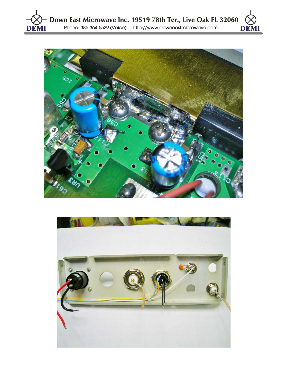
24. Power module shield install.
25. Connector panel wi ri ng.
/Kits/L70-28CK.doc 41 Rev. A 4/21/2011

26. AUX, PTT and ANT connector w iring
27. Correct coax preparation
/Kits/L70-28CK.doc 42 Rev. A 4/21/2011

28. Connector panel inst allation and wiring.
29. Coax and Ground wire install.
/Kits/L70-28CK.doc 43 Rev. A 4/21/2011

30. LO wiring and LO switch.
31. Power meter install, f ront panel wiring and LO shield install.
32. The inside view of compl eted transverter.
33. Rear view of transverter and fan install.
/Kits/L70-28CK.doc 44 Rev. A 4/21/2011

34. Front view of transverter.
/Kits/L70-28CK.doc 45 Rev. A 4/21/2011
 Loading...