

Page 1
DEM 13ULNACK
2.3 -2.45GHz. PHEMT LNA amplifier complete kit assembly guide
SPECIFICATIONS
Noise Figure: < 0.7 dB
Gain: > 15 dB
Frequency Range: 2300 - 2450 MHz
Input Voltage: 7 - 16 VDC
Description:
The 13ULNACK is a complete kit of our 13ULNA low noise amplifier designed by
W5LUA and Down East Microwave Inc. It comes complete with a pre-drilled weather-proof
enclosure, a machined pallet for mounting the PC board, the connectors of choice, (SMA or
“N”) and the standard 13ULNAK PC board kit. When completed, the DC power may be
supplied through a feed through connector or through the coax. The LNA may be mast
mounted but it is a receive only preamplifier and would require coaxial relay switching for
transceive operation!
Before starting assembly, read through the entire assembly guide. Review all of the
assembly and test procedures. Have all of your questions answered by further reading, trial
fitting, or calling DEMI for help. When you are sure of yourself, begin the assembly with
confidence and have fun!
Begin Assembly:
The circuit board needs minor preparation. Find the circuit board and the machined
pallet. Place the circuit board on top of the pallet so that the cut outs on the PCB are aligned
with the cutouts on the pallet. Note that some of the corners of the PCB (4 of them) extend
beyond the pallet edges. They need to be trimmed so that they do not extend past the edge
of the pallet. Use a knife of a diagonal cutter. If the corners are left, they will interfere with
the enclosure and lift the circuit board up from the pallet in the complete assembly causing
some component damage.
The next step is to attach the copper foil to the bottom side of the PCB. This is done
to maintain proper grounding of the RF connectors to the circuit board through the enclosure.
See figure 1 for the assembly details. The foil supplied is 2” x 1”. Cut it in half. Solder the
foil as shown. Be sure the foil is smooth and clean to start. Any bumps or crinkles in the foil
on the bottom of the PCB will push the PCB up off of the pallet and not allow the RF
connector to fit correctly. When you are finished soldering the foil, use a small file to make
the bottom of the PCB smooth. Be careful not to tear the foil!
/Kits/13ulnack.doc 1 8/12/2007
Page 2
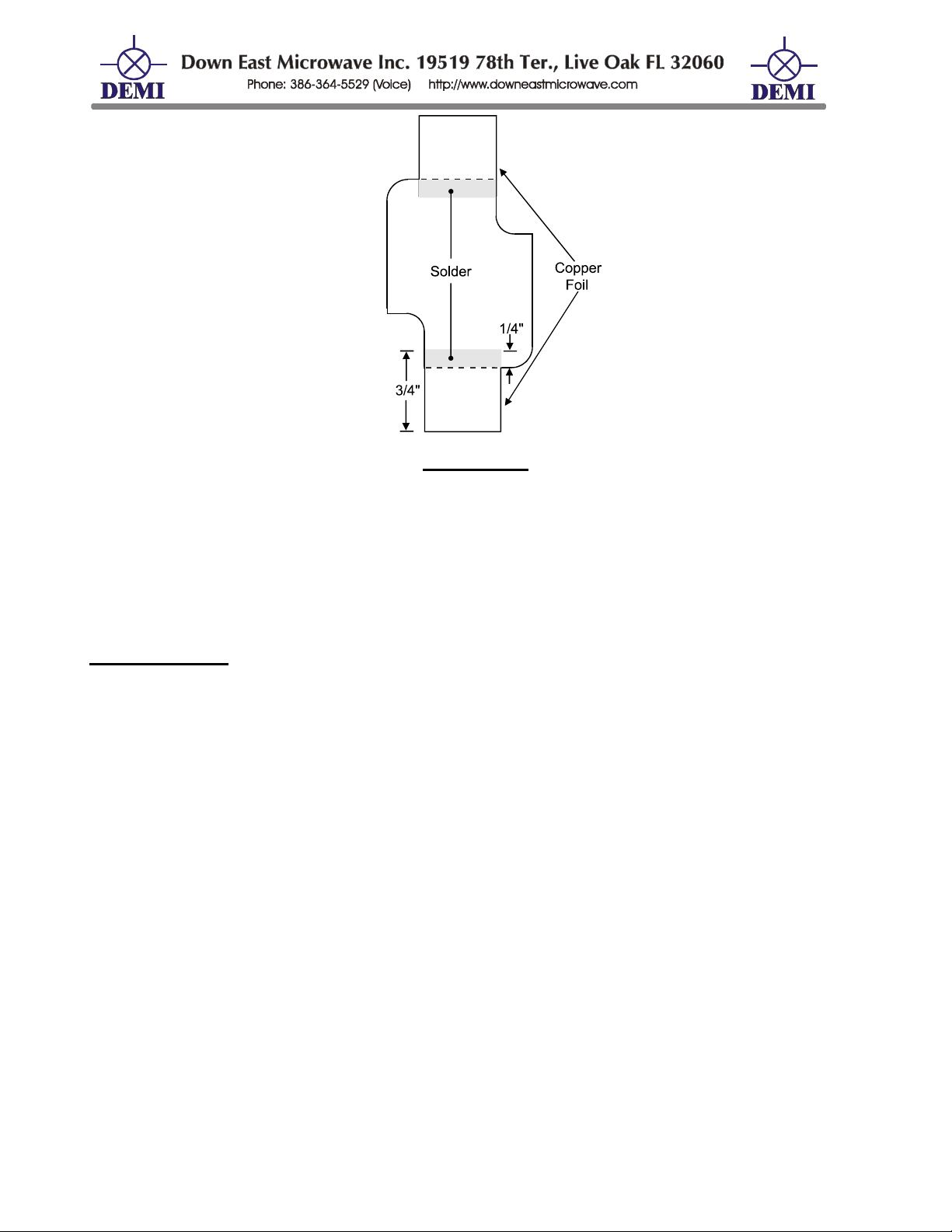
FIGURE 1.
After the foil attachment is complete, place the PCB on the pallet again and wrap the
foil around the ends of the pallet. Center the PCB on the pallet side to side. Using a small
piece of tape, (Cellophane or electrical) attach the copper foil on the back side of the pallet.
Be sure not to attach any tape on the foil that is on the end of the pallet. The ends need to be
flat and clean of all debris or it will either not fit into the enclosure or will not allow complete
grounding of the pallet.
PCB Assembly:
Assembly is easy but follow some standard ESD precautions. Use a grounded solder
iron if possible. Be sure you are discharged of static before handling IC1 or Q1. All other
components are ESD resilient but are attached to the circuitry which contain IC1 and Q1.
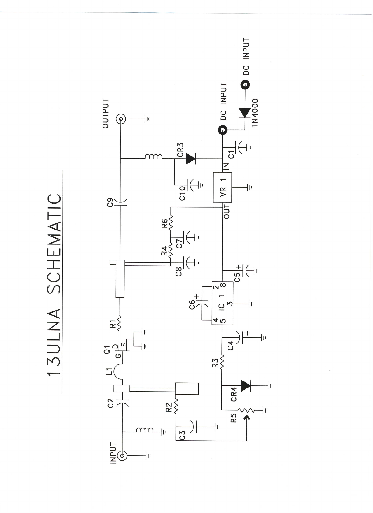
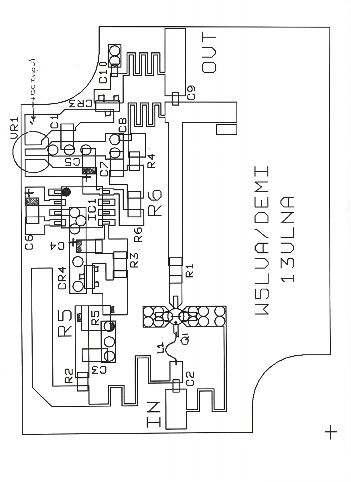
Using the component placement diagram and the electronic components parts list,
begin to assemble the PCB by installing IC1 first. Pin 1 is marked on the placement diagram.
Solder pin 3 first. This is the ground pin. Check for alignment of the other pins and if OK,
proceed to solder the other 7 pins in any order. Check for solder shorts with ohm meter.
Next attach Q1. Follow the dot shown on the component placement, align and solder the
drain lead first (the output lead or the lead connected to R1). Check the alignment and then
solder the source leads (the 2 leads on the ground plane with the via holes). You may find
the source leads difficult to solder because the heat from the iron is sunk away through the
via holes to the ground plane and pallet. A trick is to not apply to much pressure with the
solder iron to the PCB when soldering. The gate lead (or input lead) is not attached yet.
Install all other components on the circuit board in any order except C2, R1, C9, L1 and VR1.
All ground connections have multiple ground vias and may be difficult to solder. Easy on the
solder iron pressure! Solder multiple connection pads last. Review figure 2 below for correct
installation of surface mount components. Be sure to check the polarity of C5, C6, and C4. It
is indicated on the component placement guide.
/Kits/13ulnack.doc 2 8/12/2007
Page 3
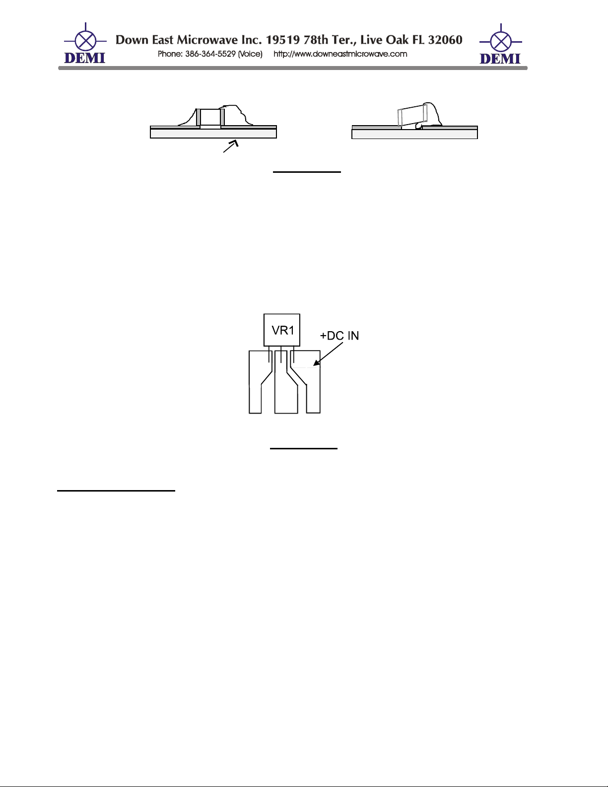
Correct
Solder Fillet
Incorrect Component
Placement
Incorrect
Circuit board
FIGURE 2.
When complete, check for missing solder, missing components, or shorts. Feel free to
use a ohmmeter for testing any connection. To Test Q1 with a ohm meter, verify that the
drain lead is not shorted to the source. It should be between 6 and 15 ohms to ground. Be
sure to Zero your meter first. The gate should be in the Kilo-ohm region. Now install VR1 as
shown in figure 3. VR1 is installed by cutting the leads short and soldering them to the circuit
laying flat with the labeling facing up.
FIGURE 3.
Hardware Assembly:
The mechanical fit is very important to the function of this LNA and everything should fit
very snug. This is the reason for trail fitting the parts before final assembly. Insert both RF
connectors in the holes on the enclosure. Trim the Teflon flush with the inside of the enclosure
with a sharp knife. Clean off the rough edges and check the fit again. Re-trim if needed.
Because the wall thickness may vary side to side note which connector goes where. Then cut
the center pin of the connectors so that only 1/8” sticks out past the Teflon. File off rough edges
if needed.
Drop the pallet into the enclosure for a trial fit. It is asymmetrical so it will fit in any
direction but be sure that the side with the 8-32 hole in it is on the same side as IC1. It should
also be a snug fit. Be sure it drops in all of the way. If not check the foil for solder build-up or if
the pallet is misaligned. Check for correct alignment of the connector holes and the RF circuit on
the PCB. Trial fit the connectors in the enclosure to verify that the pins line up with the circuitry.
The pallet has some side to side “Slop” in the enclosure to ensure proper pin alignment. If
everything looks like it will fit, install the connectors. Use a silicone sealant if you require
complete weather proofing of the enclosure. Use it conservatively and be careful not to get any
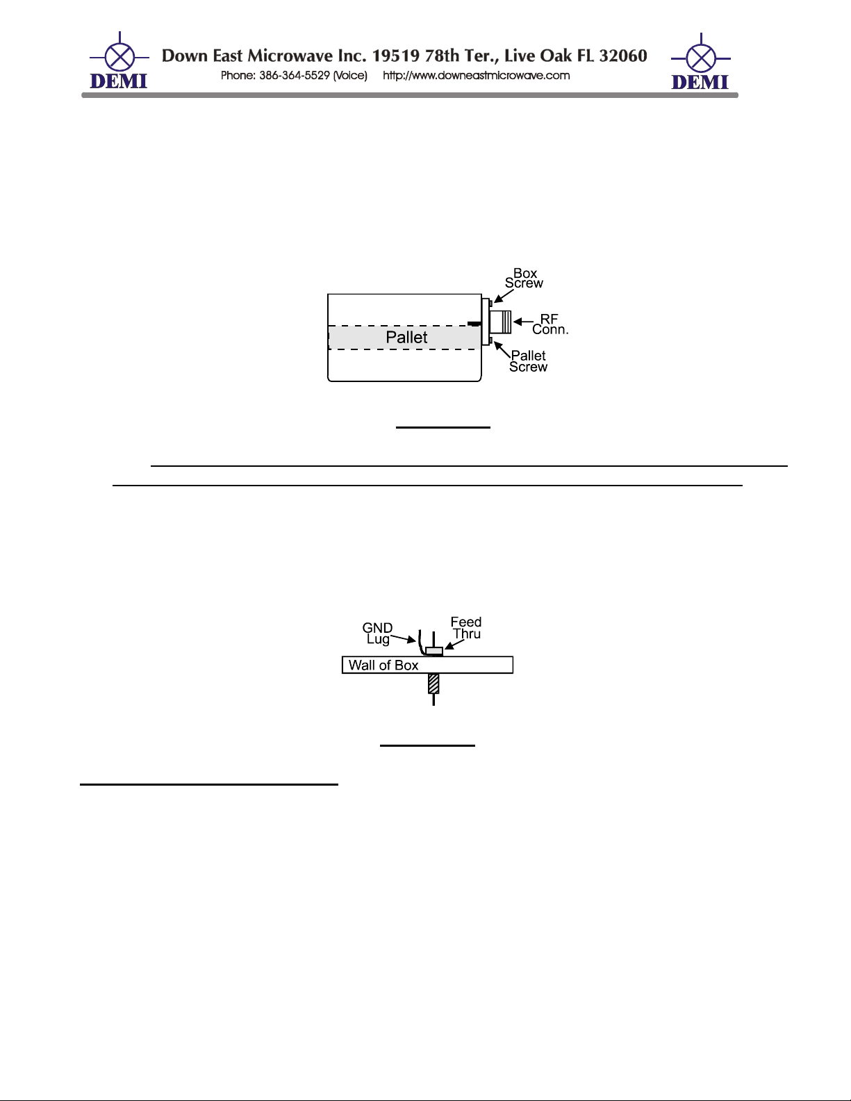
on the Teflon or the pin. Install the RF connectors by starting with the 4-40 x 3/16” box screws
first on both connectors (see figure 4) make them snug but do not tighten. Align the pallet and
PCB so that the pin of the connectors are on the input and output pads. Then poke a hole in the
/Kits/13ulnack.doc 3 8/12/2007
Page 4
copper foil through the connector screw holes with a sharp object or small drill bit before installing
the pallet screws. If you install the screw and force it to penetrate the foil, it will cause the screw
to bind and damage the threads in the pallet. Do not remove the pallet after making the holes in
the foil. After the threaded holes are cleared of foil, install the 4-40 x 3/8” pallet screws. Check
for alignment then begin to tighten the input connector first, pulling the pallet towards the
enclosure and ensuring a tight fit. This is best for stability and noise figure. Then tighten the
output connector screws last. Re-tighten all of the screws. Check for alignment and if satisfied,
install C2, C9 and solder the RF connector pins.
FIGURE 4.
Warning: Do not tighten any screws after the center pins are soldered! This may tear the center
pin from the circuit board. Be sure that all screw are absolutely tight before soldering!
Install the 8-32 Feed-thru connector and ground lug (see Figure 5) in the remaining hole
of the enclosure. Again if you want a weatherproof enclosure, apply some sealant to the
connector before installing. Connect the 1N4000 type diode between the DC feed-thru connector
and the point on the component placement labeled “+DC Input” This is a reverse polarity
protection diode.
FIGURE 5.
Pre-Testing and Final Assembly:
Preliminary testing is required before final assembly and testing the RF circuit. With
R1and L1 still not installed, the drain and gate voltage will not be connected to Q1 so voltage
may be applied to the feed through without endangering Q1.
Apply a DC input of +7 to +17 VDC to the feed through connector and ground lug.
Measure +5VDC on the output side of VR1. Verify that the +5VDC travels through the drain
circuit biasing to the Junction of where R1 is to be assembled. If it is not there, find the open
circuit and repair. Now verify that the gate bias is functioning correctly. Measure the voltage
on the Q1 side of C2. It should be less than -0.8VDC. (negative voltage!) Adjust R5 to obtain
-0.5VDC. Again if any of the voltages can not be obtained, trace the circuit for problems.
There should be -5 VDC on pin 5 of IC1. If all voltages check out, install L1. Bend the gate
lead of Q1 up to form an approximate 45 degree angle to the PC board. Solder a single
strand of wire from the green wire found in the kit to the pad shared by C2. After soldering,
extend the length of the strand straight up perpendicular to the PC board. Measure the
/Kits/13ulnack.doc 4 8/12/2007
Page 5
length of the strand and cut it to 0.400” long. Form a loop and solder the lose end to the gate
lead of Q1 close to the package . Try not to disturb the angle of the lead. Re-apply the +DC
voltage and check for the -0.5VDC at the junction of C2 and L1 to verify that the gate lead
in not shorted. If it checks out, remove the DC voltage from the LNA and install R1.
Final Testing:
Install a 50 ohm load to both input and output connectors. This can be a termination,
an antenna, or a receiver. Apply the DC voltage to the feed through connector and verify that
the drain lead has voltage. It should be between 2 and 5 volts DC. Now measure the drain
current. This is either measured across R6 (100 ohm resistor with the use of Ohms law) or
may be measured directly on the +DC supply line. The drain current should be between 15
and 20 mA. The drain current can now be adjusted by varying R5. As the gate voltage
approaches 0VDC, the drain current will increase. If the gate voltage is adjusted more
negative, the drain current will decrease. Adjust R5 for approximately 15-20 mA of drain
current.
If the DC testing is correct, the LNA will be operating correctly and the RF adjustments
should not be attempted unless you have a way of measuring Gain and/or Noise Figure. Just
re-test the Dc current drain to ensure proper operation. Even if you do have the equipment
available, there will only be minimal adjustments, if any, to be made to improve the
performance of the LNA. If it is assembled correctly and the bias is set correctly, the LNA will
perform correctly.
Component List
All resistors are 1206 size chips. The white band is positive on the Tantalum chip
capacitors. All other capacitors are various sizes.
C1 0.1µF C6 10.0 µF
C2 8.2 ρF ATC C7 0.1µF
C3 0.1µF C8 8.2 ρF ATC
C4 10.0 µF C9 8.2 ρF ATC
C5 1.0 µF C10 8.2 ρF ATC
CR3 MMBD914 R1 15 R5 1K pot
CR4 MMBD914 R2 51 R6 100
IC1 7660 SMD R3 5.1K VR1 78L05
L1 0.4” Strand R4 51 PC Board
Q1 ATF36077
Hardware Parts List
1 - Weather- proof enclosure complete with gasket 4 - 4-40 x 3/8” screws
1 - Machined aluminum pallet 4 - 4-40 x 3/16” screws
2 - RF connectors , SMA or “N” 1 - #8 ground lug
1 - Copper foil 2” x 1” 4 - flat head cover screws
1 - #8-32 feed-thru connector 1 - 1N4000 type diode
/Kits/13ulnack.doc 5 8/12/2007
Page 6
Page 7
 Loading...