

Page 1
Noise Figure:
< 0.6 dB
Gain:
> 15 dB
Frequency Range:
2300 - 2450 MHz
Input Voltage:
7 - 16 VDC
Current Drain:
< 30 mA.
L13ULNA
DESCRIPTION:
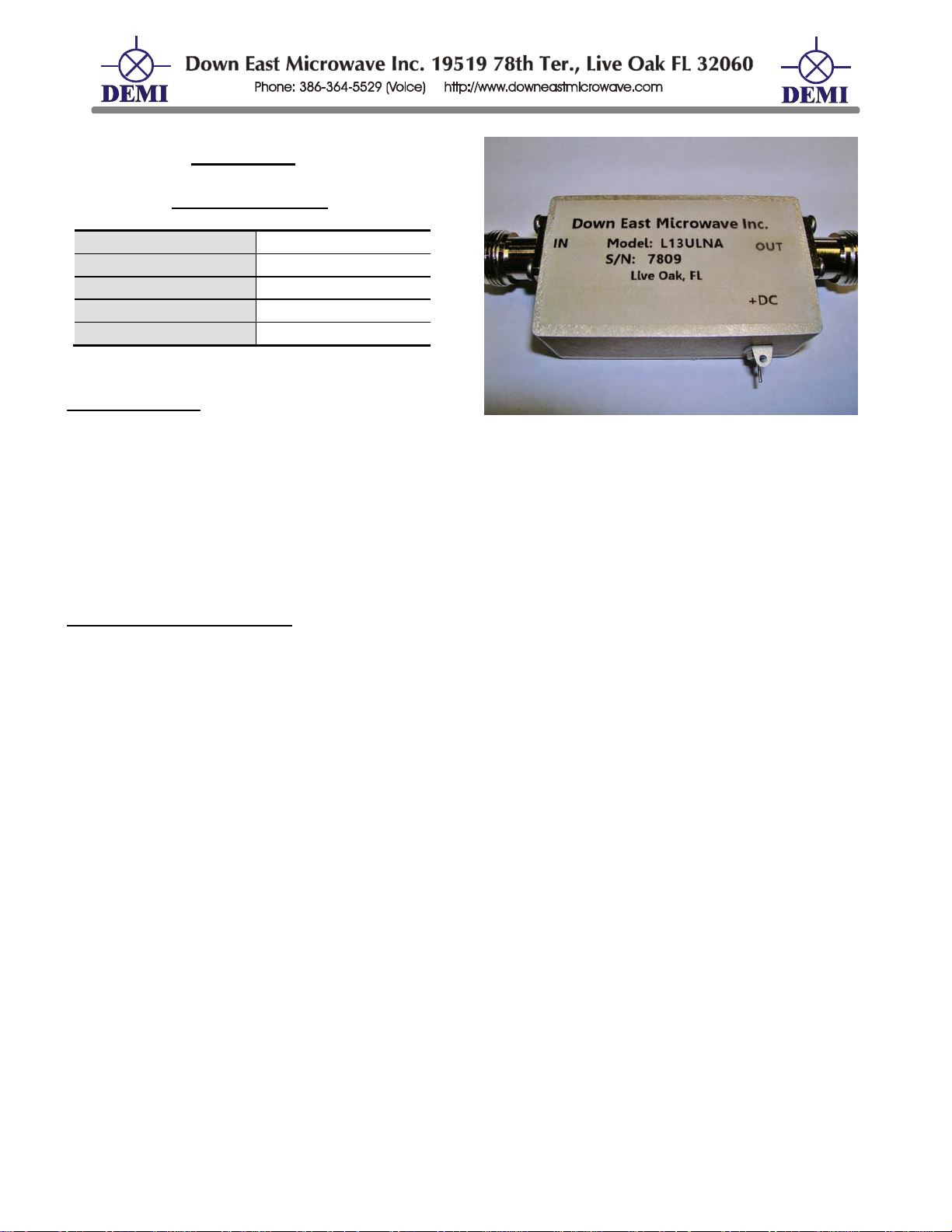
The 13ULNA is a low noise amplifier designed by W5LUA and Down East Microwave Inc.
using the latest PHEMPT technology. This LNA was designed for receive only purposes including
Phase IIID, EME, and other standard weak signal reception between 2300 and 2450 MHz. The
LNA is assembled in a machined chemical etched enclosure and has the option of two connector
types, either SMA or Type “N” that is specified when ordering. This design can be biased either
through the coax or through the external DC feed through connector in its standard form. There is
no need to specify. Custom models are available to cover band segments from 2100 - 2500 MHz.
INSTALLATION and USE:
Depending on your application, the LNA may be installed anywhere in your system to
increase gain. To maintain or improve the systems noise figure requires the LNA to be installed as
close to the systems antenna as possible. If you are using this LNA in a transceive system with
transmit bypass relays, be sure of their isolation characteristics and transmit power handling
capabilities before transmitting. Use only interconnecting cables and adapters that are rated for
use at or above 2.5 GHz. Inadequate cabling or cables with poor shielding may cause system
instabilities, signal loss, or undesirable intermittent operation.
The connector marked INPUT, is to be connected to the antenna. The OUTPUT is
connected to the receiver. The output connector accepts only DC bias between +7 and +16 volts.
This may be supplied by the receiver or a DC power inserted located between the LNA output and
the receiver input. If using coaxial transfer relays in the system with DC bias on the coax, be sure
that shorting type relays are not used in the receive path in a way that the DC is connected to
ground when the LNA is switched out of line.
The input circuit of the LNA is DC shorted for static protection. This a useful feature when
using antennas such as a dish with a wave guide fed or a helical type antenna that are not DC
grounded. This DC short will protect the LNA when it is installed in a remote location but does
degrade the noise figure by 0.1dB. The LNA will not withstand a direct lightning hit. Other
precautions will need to be made for such an instance.
SPECIFICATIONS
/Built/13ULNA.doc 1 Rev. A 11/9/16
Page 2
OPERATING:
Expected performance should be overall improvement in gain and noise figure of the
receive system with the LNA correctly installed. The proper installation of a LNA becomes more
and more important at these frequencies and because of the developments in the ISM bands,
interference will increase in the future. The gain bandwidth of the LNA design is wide to obtain a
low noise figure. Therefore, certain conditions may cause overloading of your receiver producing
intermodulation. It is always suggested to use adequate filtering between gain stages and to
practice gain management by not cascading amplifiers to solve system noise problems. Use of
directional antennas will also increase desired signals and aid in elimination of undesired signals in
the 13cm band.
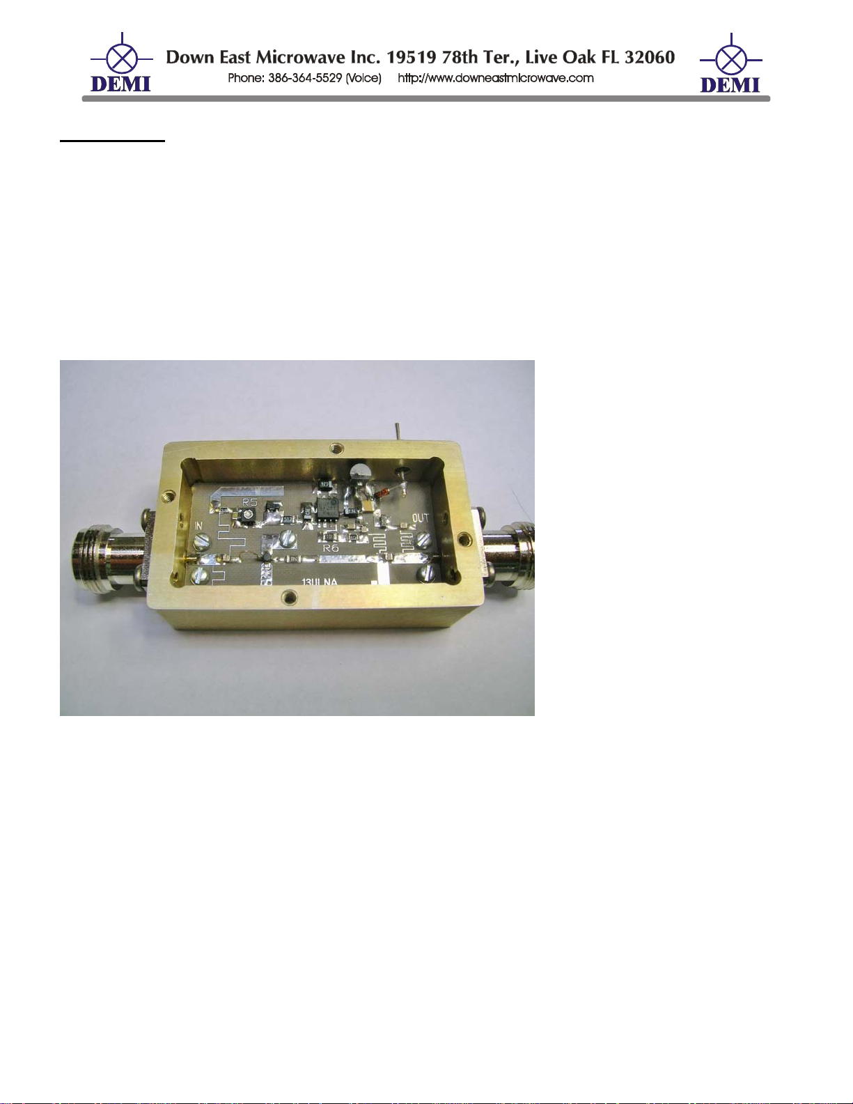
For use in EME or weak
signal type systems, the
elimination of the shorted line on
the input circuit may be desired.
If so, open the lid by removing
the 4 screws, and with a sharp
knife, cut the printed inductor
line as close to the RF input
circuit as possible. This may
only slightly improve the noise
figure and may not be worth
giving up the static protection in
a tropo only system. If you are
not biasing the LNA through the
coax, eliminating the printed
inductor on the output connector
will only net you only a maximum
of 0.3dB gain.
If you are biasing the LNA through the coax, there is no need to insulate the DC feed
through connector. There will be no measurable voltage on the Feed through and it will not
disable the LNA if shorted accidentally.
/Built/13ULNA.doc 2 Rev. A 11/9/16
Page 3
IC1 7660 SMD
R4 51
C2 8.2 pF ATC
C8 8.2 pF ATC
L1 0.4” Strand
R5 1K pot
C9 8.2 pF ATC
Q1 NE3210
R6 100
C10 8.2 pF ATC
R1 15
VR1 78L05
C5 1.0 µF Tant.
CR3 MMBD914
R2 51
CR4 MMBD914
R3 5.1K
IC 1
+
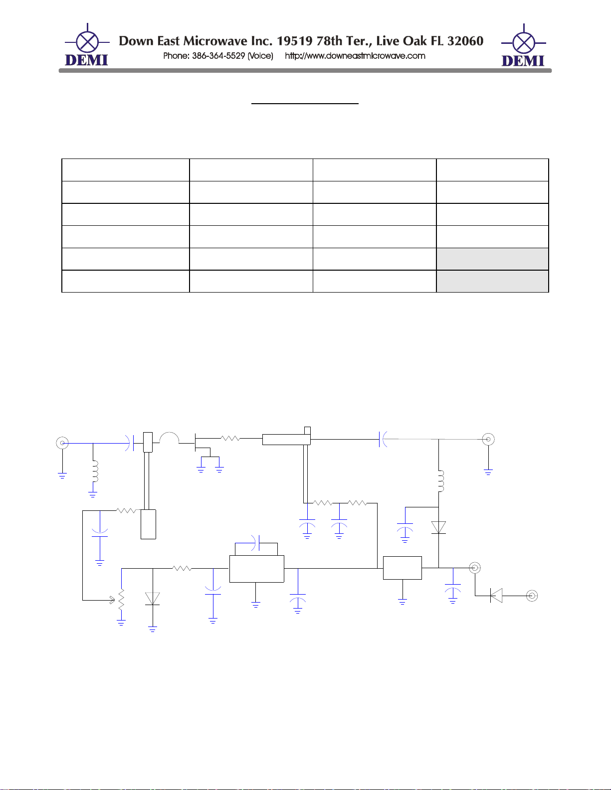
13ULNA SCHEMATIC
+
+
INP UT
OUTPUT
DC IN PUT
VR 1
C2
L1
D
R1
R2
C3
R5
Cr4
C4
R3
C5
CR3
C10
R6
R4
C7
C8
C6
C9
S
G
Q1
C1
IN
OUT
8
24
5
3
1N4000
DC IN PUT
COMPONENT LIST
All resistors are 1206 size chips unless indicated. The white band is positive on the Tantalum chip
capacitors. All other capacitors are various sizes.
C1 0.1µF C7 0.1µF
C3 0.1µF
C4 10.0 µF Tant.
C6 10.0 µF Tant.
/Built/13ULNA.doc 3 Rev. A 11/9/16
 Loading...