

Page 1
^1 HARDWARE REFERENCE MANUAL
^2 Compact UMAC
Turbo CPU Board
^3 Turbo CPU Board
^4 4Ax-603625-xUxx
^5 January 17, 2006
Single Source Machine Control Power // Flexibility // Ease of Use
21314 Lassen Street Chatsworth, CA 91311 // Tel. (818) 998-2095 Fax. (818) 998-7807 // www.deltatau.com
Page 2

Copyright Information
© 2005 Delta Tau Data Systems, Inc. All rights reserved.
This document is furnished for the customers of Delta Tau Data Systems, Inc. Other uses are
unauthorized without written permission of Delta Tau Data Systems, Inc. Information contained
in this manual may be updated from time-to-time due to product improvements, etc., and may not
conform in every respect to former issues.
To report errors or inconsistencies, call or email:
Delta Tau Data Systems, Inc. Technical Support
Phone: (818) 717-5656
Fax: (818) 998-7807
Email: support@deltatau.com
Website: http://www.deltatau.com
Operating Conditions
All Delta Tau Data Systems, Inc. motion controller products, accessories, and amplifiers contain
static sensitive components that can be damaged by incorrect handling. When installing or
handling Delta Tau Data Systems, Inc. products, avoid contact with highly insulated materials.
Only qualified personnel should be allowed to handle this equipment.
In the case of industrial applications, we expect our products to be protected from hazardous or
conductive materials and/or environments that could cause harm to the controller by damaging
components or causing electrical shorts. When our products are used in an industrial
environment, install them into an industrial electrical cabinet or industrial PC to protect them
from excessive or corrosive moisture, abnormal ambient temperatures, and conductive materials.
If Delta Tau Data Systems, Inc. products are exposed to hazardous or conductive materials and/or
environments, we cannot guarantee their operation.
Page 3

UMAC-CPCI Turbo CPU Board Hardware Reference Manual
Table of Contents
INTRODUCTION .......................................................................................................................................................1
Associated Manuals...................................................................................................................................................1
BOARD CONFIGURATION.....................................................................................................................................2
Option 1: Communications Interfaces......................................................................................................................2
Current Revision Communication Options (rev 103 and above)..........................................................................2
Legacy Revision Communication Options (rev 102 and below)...........................................................................2
Option 2: Dual-Ported RAM .....................................................................................................................................2
Option 5: CPU and Memory Configurations.............................................................................................................2
Current Revision Memory Options (Rev 103 and above).....................................................................................3
Legacy Revision Memory Options (Rev 102 and below) ......................................................................................4
Option 8: High-Accuracy Clock Crystal ..................................................................................................................4
Option 9: Serial Port Configuration .........................................................................................................................4
Option 10: Firmware Revision Specification ...........................................................................................................4
Option 16: Battery-Backed Parameter Memory........................................................................................................4
HARDWARE SETUP .................................................................................................................................................5
Clock-Source Jumpers...............................................................................................................................................5
Watchdog Timer Jumper...........................................................................................................................................5
Operation Mode Jumpers ..........................................................................................................................................5
Firmware Reload Jumper ..........................................................................................................................................5
Re-Initialization Jumper............................................................................................................................................5
Serial-Port Level Select Jumpers...............................................................................................................................6
DPRAM IC Select Jumper ........................................................................................................................................6
Flash IC Firmware Bank Select Jumpers ..................................................................................................................6
Flash IC Power Supply Select Jumper ......................................................................................................................6
Power-Supply Check Select Jumper .........................................................................................................................6
Reset-Lock Jumper....................................................................................................................................................6
CONNECTIONS .........................................................................................................................................................7
Compact UBUS Connector .......................................................................................................................................7
Rear Field Wiring Connector ....................................................................................................................................7
Front-Panel RS-232 Connector .................................................................................................................................7
Stack Connectors to Bridge Board ............................................................................................................................7
Factory-Use Connectors............................................................................................................................................8
BOARD LAYOUT.......................................................................................................................................................9
Current Revision Layout Diagram (rev 103 and above) ...........................................................................................9
Legacy Revision Layout Diagram (rev 102 and below)..........................................................................................10
JUMPER DESCRIPTIONS......................................................................................................................................11
E0: Reset-Lock Enable (Factory Use Only)...........................................................................................................11
E1A: Servo and Phase Clock Direction Control.....................................................................................................11
E1B: Servo/Phase Clock Source Control ...............................................................................................................11
E2: (Reserved for Future Use)................................................................................................................................11
E3: Re-Initialization on Reset Control ...................................................................................................................12
E4: (Reserved for Future Use).................................................................................................................................12
E5: USB/Ethernet Communication Jumper............................................................................................................12
E11: Power Supply Check Control.........................................................................................................................12
E17 – E18: Serial Port Select .................................................................................................................................12
E18A, B, C, D: Ethernet Communication Control.................................................................................................13
E19: Watchdog Disable Jumper.............................................................................................................................13
E20 – E22: Power-Up/Reset Load Source .............................................................................................................13
E23: Firmware Reload Enable................................................................................................................................13
Page 4

UMAC-CPCI Turbo CPU Board Hardware Reference Manual
E25A, B, C: Flash Memory Firmware Bank Select ...............................................................................................13
W1: Flash IC Power Supply Select Jumper............................................................................................................14
CONNECTOR SUMMARY.....................................................................................................................................15
CONNECTOR PINOUTS.........................................................................................................................................17
Compact UBUS Connector (J1) Pinout...................................................................................................................17
Compact UMAC Turbo CPU Board J2 Connector .................................................................................................18
J4: RS-232 Serial Port Connector...........................................................................................................................19
ACCESSORIES.........................................................................................................................................................21
Acc-Cx Compact UBUS Backplane Boards ...........................................................................................................21
Acc-8CR Test Breakout Board................................................................................................................................21
Acc-11C Sinking I/O Board....................................................................................................................................21
Acc-24C2 PWM Axis Board...................................................................................................................................22
Acc-24C2A Analog Axis Board..............................................................................................................................22
Acc-51C Analog Encoder Interpolator Board.........................................................................................................22
SCHEMATICS ..........................................................................................................................................................23
Table of Contents
ii
Page 5
UMAC-CPCI Turbo CPU Board Hardware Reference Manual
INTRODUCTION
Delta Tau’s Compact UMAC systems provide a compact and clean integration of motion and I/O control
for sophisticated automation equipment. The Compact UMAC CPU was previously called the UMACCPCI in previous revisions of this manual. The system consists of a modular set of 3U-size (100mm x
160mm) boards in the Compact PCI format, implementing Turbo PMAC software and hardware
functions, communicating with each other over a common backplane (the “Compact UBUS”). All field
wiring is available on rear connectors, suitable for a user-designed distribution system to the machine.
Compact UMAC (Universal Motion and Automation Controller) -CPCI systems provide integrated
connectivity as well as ease of assembly, diagnostics, and repair. Compact UMAC systems differ from
standard UMAC systems in that all field wiring comes to the back of the rack, behind the backplane,
instead of direct top and bottom access.
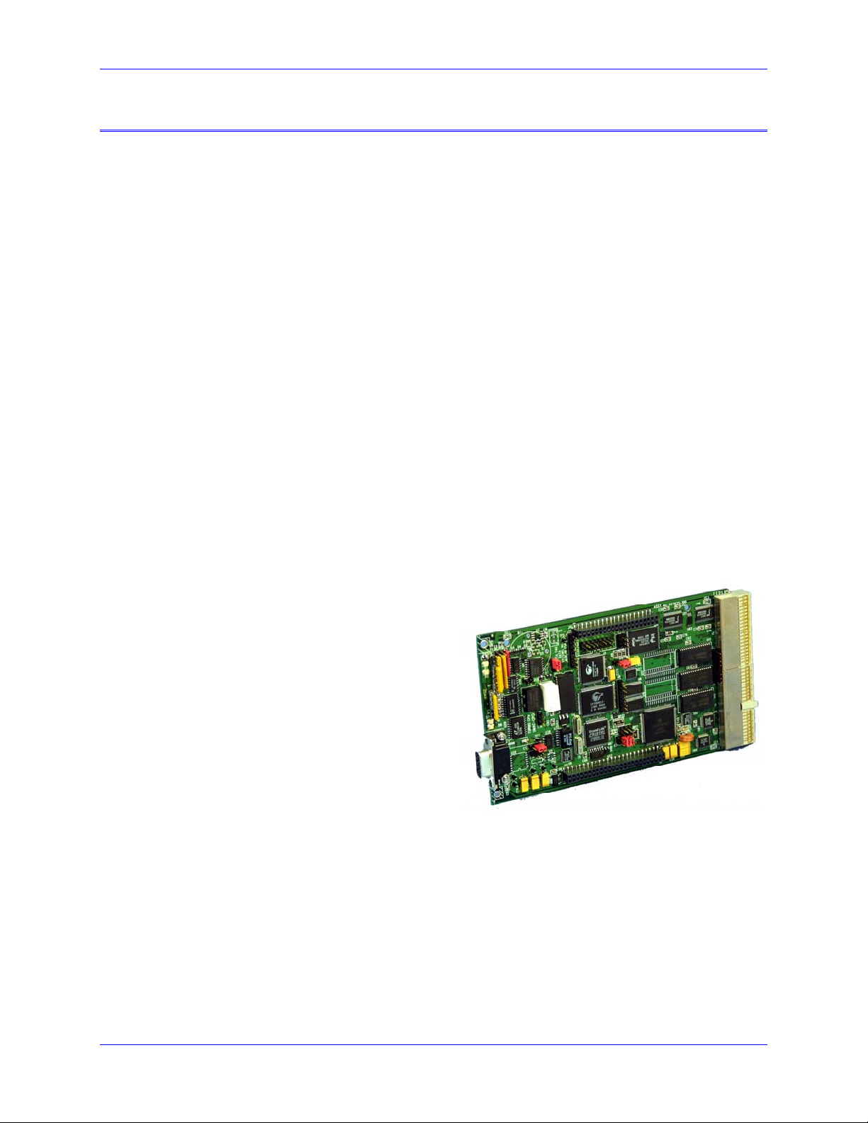
The Compact UMAC Turbo CPU board (Part number 3A0-603625-10x) implements a Turbo PMAC2
CPU in the 3U CPCI form factor. Its software operation is completely identical to other Turbo PMAC2
controllers.
The 603625 Compact UMAC Turbo CPU has two hardware versions that will be covered in this manual.
The difference between the two is the Flex CPU design upgrade on all new revisions released after the
spring of 2005. The Flex CPU allows the board to use an 80 MHz CPU, 160 MHz CPU, or 240 MHz
CPU. The old design allowed a maximum CPU speed of 100 MHz. The revision number is designated
by the last three numbers of the part number. For example, the part number for the current revision
release is the 603625-104 and we would call the board a revision 104 release. The legacy model CPU was
the 603625-102 and it would be designated as a revision 102.
Note that a Compact PCI interface does not come with a Compact UMAC system automatically, nor is
one necessary to communicate to the system, given the other possible communications ports: RS-232,
RS-422, USB, and Ethernet.
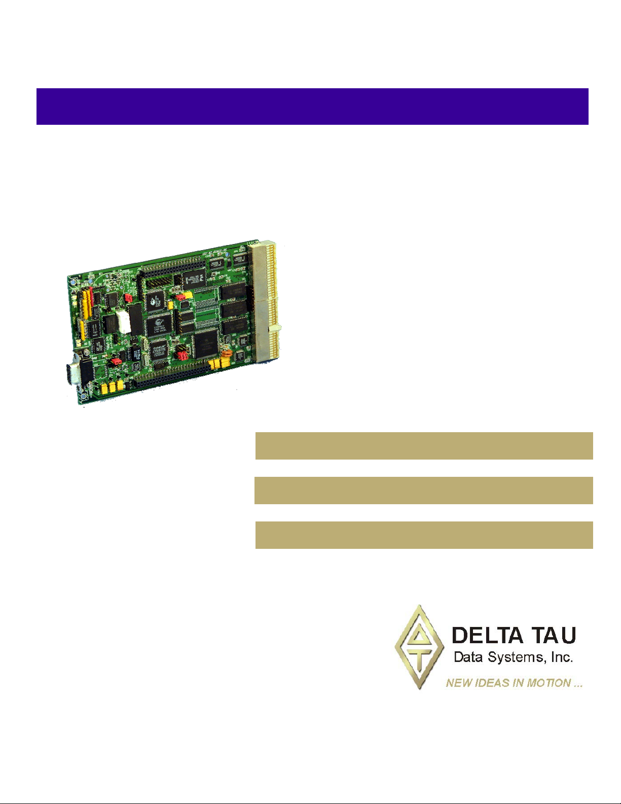
This picture shows the Compact UMAC Turbo CPU
board. The connectors on the right side plug into the
Compact UBUS backplane board, with the bottom
right connector being the bus connector, and the top
right connector containing the external field wiring
signals, which typically pass through the backplane
board. The connector at lower left is an RS-232 port
intended for setup and diagnostics; the stack
connectors top and bottom provide the link to a CPCI
bridge board.
Introduction 1
Page 6
UMAC-CPCI Turbo CPU Board Hardware Reference Manual
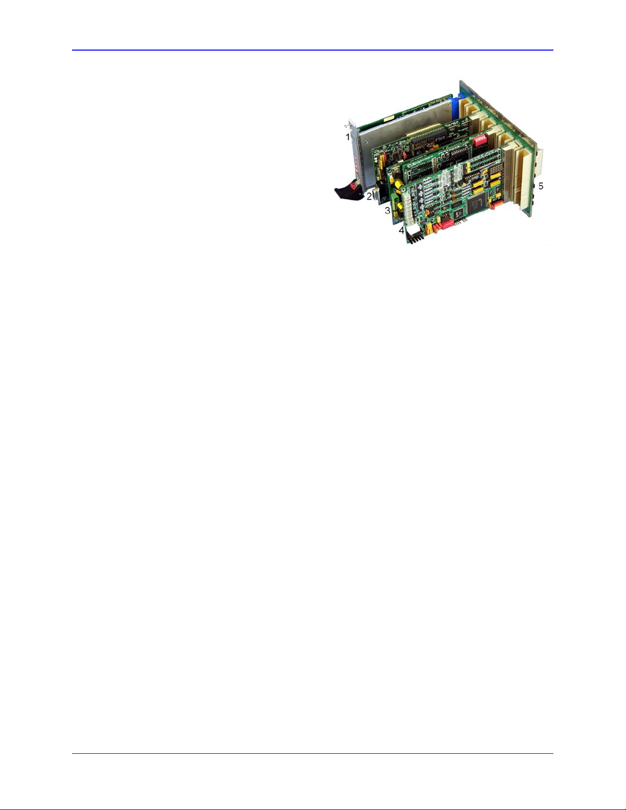
This picture shows a sample configuration of a
Compact UMAC system, not installed in its rack. It
consists of the following components:
1. Rack power supply (not a Delta Tau product)
2. Compact UMAC CPU board
3. Acc-11C Sinking I/O board
4. Acc-24C2A analog axis interface board
5. Acc-C8 8-slot Compact UBUS backplane.
Note the pass-through connector on the back
for field-wiring distribution. In this picture,
alternate slots in the backplane have been left
open to make each board more visible. This
does not have to be done in actual use.
2 Introduction
Page 7

UMAC-CPCI Turbo CPU Board Hardware Reference Manual
Associated Manuals
This document is the Hardware Reference Manual for the Compact UMAC Turbo CPU board for an
Compact UMAC system. It describes the hardware features and provides setup instructions.
Other manuals are needed as well to use the Compact UMAC system. Each accessory to the Compact
UMAC Turbo CPU board has its own manual, describing its operation and any required software setup of
the Turbo CPU.
The Software Reference Manual for the Turbo PMAC family and the User Guide for the PMAC or Turbo
PMAC families are also needed.
Introduction 1
Page 8

UMAC-CPCI Turbo CPU Board Hardware Reference Manual
BOARD CONFIGURATION
The base version of the Compact UMAC Turbo CPU board provides a 1-slot 3U-format Eurocard board
with:
80 MHz DSP56303 CPU (120 MHz PMAC equivalent) •
•
128k x 24 SRAM compiled/assembled program memory (Opt. 5C0)
•
128k x 24 SRAM user data memory (Opt. 5C0)
•
1M x 8 flash memory for user backup & firmware (Opt. 5C0)
•
Latest released firmware version
•
RS-232/422 serial interface, available both on front-panel DB-9 connector and on backside fieldwiring connector
•
Backplane Compact UBUS expansion connector for communication to servo and I/O accessory
boards
•
Backside field-wiring connector
Option 1: Communications Interfaces
The Compact UMAC Turbo CPU board comes standard only with an RS-232/422 serial interface. The
Option 1 family provides faster interfaces for high-speed communications – Universal Serial Bus (USB),
Ethernet, or the link to the CPCI bus through a bridge daughter board.
Current Revision Communication Options (rev 103 and above)
Option 1: 100 Mbit/sec UDP/IP, TCP/IP Ethernet Communications Interface. •
•
Option 1A: 480 Mbit/sec USB 2.0 Communications Interface (USB 1.1 compatible)
•
Option 1B: Solder-side stack connectors to CPCI-bridge daughter board. This option should be ordered
only when the bridge board is to be installed on the left side of the CPU board, so the CPU board is in the
leftmost slot of the Compact UBUS backplane, and the bridge board is in the rightmost slot of the
Compact PCI bus backplane.
Legacy Revision Communication Options (rev 102 and below)
•
Option 1: On-board 10-Base-T TCP/IP Ethernet interface. The key added components are U67 and U32.
•
Option 1A: On-board 12 Mbit/sec USB interface. The key added component is U67.
•
Option 1B: Solder-side stack connectors to CPCI-bridge daughter board. This option should be
ordered only when the bridge board is to be installed on the left side of the CPU board, so the CPU
board is in the leftmost slot of the Compact UBUS backplane, and the bridge board is in the rightmost
slot of the Compact PCI bus backplane.
Option 2: Dual-Ported RAM
With either the Option 1 Ethernet interface, or the Option 1A USB interface, communications throughput
can be increased through the use of dual-ported RAM, which provides a bank of memory that can be
directly accessed by both the Compact UMAC Turbo CPU and the communications microcontroller.
Option 2: 32k x 16 bank of on-board dual-ported RAM (requires Option 1 or 1A) in component U56. •
Option 5: CPU and Memory Configurations
The various versions of Option 5 provide different CPU speeds and main memory sizes on the piggyback
CPU board. Only one Option 5xx may be selected for the board.
2 Board Configuration
Page 9

UMAC-CPCI Turbo CPU Board Hardware Reference Manual
The CPU is a DSP563xx IC as component U1. It is currently available only as an 80 MHz, 160 MHz or
240 MHz device.
The compiled/assembled-program (P) memory SRAM ICs are located in U14, U15, and U16. These ICs
form the active memory for the firmware, compiled PLCs, and user-written phase/servo algorithms.
These can be 128k x 8 ICs (for a 128k x 24 bank), fitting in the smaller footprint, or they can be the larger
512k x 8 ICs (for a 512k x 24 bank), fitting in the full footprint.
The user-data memory (X/Y) SRAM ICs are located in U11, U12, and U13. These ICs form the active
memory for user motion programs, uncompiled PLC programs, and user tables and buffers. These can be
128k x 8 ICs (for a 128k x 24 bank), fitting in the smaller footprint, or they can be the larger 512k x 8 ICs
(for a 512k x 24 bank), fitting in the full footprint.
The flash memory IC is located in U10. This IC forms the non-volatile memory for the board’s firmware,
the user setup variables, and for user programs, tables, and buffers. It can be 1M x 8, 2M x 8, or 4M x 8
in capacity
Current Revision Memory Options (Rev 103 and above)
The various versions of Option 5 provide different CPU speeds and main memory sizes. Only one Option
5xx may be selected for the board.
Option 5C0 is the standard CPU and memory configuration. It is provided automatically if no Option
•
5xx is specified. It provides an 80 MHz DSP56303 CPU w/8Kx24 internal memory, 128Kx24
SRAM compiled/ assembled program memory, 128Kx24 SRAM user data memory, 1Mx8 flash
memory.
•
Option 5C3 provides an 80 MHz DSP56303 CPU w/8Kx24 internal memory, expanded 512Kx24
SRAM compiled/assembled program memory, expanded 512Kx24 SRAM user data memory, 4Mx8
flash memory.
•
Option 5E0 provides a 160 MHz DSP56311 CPU w/128Kx24 internal memory, 128Kx24 SRAM
compiled/ assembled program memory, 128Kx24 SRAM user data memory, and 1Mx8 flash
memory. Requires V1.939 or newer firmware.
•
Option 5E3 provides a 160 MHz DSP56311 CPU w/128Kx24 internal memory, expanded 512Kx24
SRAM compiled/assembled program memory, expanded 512Kx24 SRAM user data memory, and
4Mx8 flash memory. Requires V1.939 or newer firmware.
•
Option 5F0 provides a 240 MHz DSP56321 CPU w/192Kx24 internal memory, 128Kx24 SRAM
compiled/ assembled program memory, 128Kx24 SRAM user data memory, and 1Mx8 flash
memory. Requires V1.940 or newer firmware.
•
Option 5F3 provides a 240MHz DSP56321 CPU w/192Kx24 internal memory, expanded 512Kx24
SRAM compiled/assembled program memory, expanded 512Kx24 SRAM user data memory, and
4Mx8 flash memory. Requires V1.940 or newer firmware.
Board Configuration 3
Page 10

UMAC-CPCI Turbo CPU Board Hardware Reference Manual
Legacy Revision Memory Options (Rev 102 and below)
Option 5C0 is the standard CPU and memory configuration. It is provided automatically if no Option
•
5xx is specified. It provides an 80 MHz DSP56303 CPU (120 MHz PMAC equivalent) with 8k x 24
of internal memory, an external 128k x 24 of compiled/assembled program memory, an external 128k
x 24 of user data memory; and a 1M x 8 flash memory. Setup variable I52 should be set and saved at
7 for 80 MHz operation.
•
Option 5C3 provides an 80 MHz DSP56303 CPU (120 MHz PMAC equivalent) with 8k x 24 of
internal memory, an expanded external 512k x 24 of compiled/assembled program memory, an
expanded external 512k x 24 of user data memory, and a 4M x 8 flash memory. Setup variable I52
should be set and saved at 7 for 80 MHz operation.
•
Option 5D0 provides a 100 MHz DSP56309 CPU (150 MHz PMAC equivalent) with 34k x 24 of
internal memory, an external 128k x24 of compiled/assembled program memory, an external 128k x
24 of user data memory; and a 1M x 8 flash memory. Setup variable I52 should be set and saved at 9
for 100 MHz operation.
•
Option 5D3 provides a 100 MHz DSP56309 CPU (150 MHz PMAC equivalent) with 34k x 24 of
internal memory, an expanded external 512k x 24 of compiled/assembled program memory, an
expanded external 512k x 24 of user data memory, and a 4M x 8 flash memory. Setup variable I52
should be set and saved at 9 for 100 MHz operation.
Option 8: High-Accuracy Clock Crystal
The Compact UMAC Turbo CPU board has a clock crystal (component Y1) of nominal frequency
19.6608 MHz (~20 MHz). The standard crystal’s accuracy specification is +/-100 ppm.
Option 8A provides a nominal 19.6608 MHz crystal with a +/-15 ppm accuracy specification. •
Option 9: Serial Port Configuration
The Compact UMAC Turbo CPU board comes standard with a single RS-232/422 serial port; a second
serial port can be added.
Option 9T adds an auxiliary RS-232 port on the CPU board. The key components added are ICs U28
•
and U43.
Option 10: Firmware Revision Specification
Normally the Compact UMAC Turbo CPU board is provided with the newest released firmware revision.
Some users may wish to freeze the designs on an older revision. A label on the U10 flash memory IC
shows the firmware revision loaded at the factory. The VERSION command can be used to report what
firmware revision is currently installed.
Option 10 provides for a user-specified firmware version. •
Option 16: Battery-Backed Parameter Memory
The contents of the standard memory are not retained through a power-down or reset unless they have
been saved to flash memory first. Option 16 provides supplemental battery-backed RAM for real-time
parameter storage that is ideal for holding machine state parameters in case of an unexpected powerdown.
Option 16A provides a 32k x 24 bank of battery-backed parameter RAM in components U17, U18,
•
and U19 and a can-stack lithium battery in component BT1. While the average expected battery life
is over five years, a yearly replacement schedule is recommended. Replacement batteries can be
ordered from Delta Tau as Acc-1LS (Part # 100-0QTC85-000).
4 Board Configuration
Page 11

UMAC-CPCI Turbo CPU Board Hardware Reference Manual
HARDWARE SETUP
Clock-Source Jumpers
In order to operate properly, the Turbo CPU board must receive servo and phase clock signals from a
source external to the board. These clock signals can be brought into the board from one of three possible
ports: the stack connector, the UBUS backplane connector, or the front-side main serial-port connector.
Jumpers E1A and E1B must be configured properly for the clock source used.
(Note: If the Compact UMAC Turbo CPU board cannot find the clock signal from the source specified by
these jumpers, it will generate its own 2.26kHz servo clock and its own 9.04kHz phase clock so it will
stay in operation.)
To receive the clock signals over the Compact-UBUS backplane, usually from an Acc-24C2x axisinterface board, E1A must connect pins 1 and 2, and E1B must connect pins 2 and 3. This configuration
is typical for an Compact UMAC system. The clock signals are output on the main serial port.
To receive the clock signals through the stack connectors, usually from the MACRO IC on the CPCI
“bridge” board, E1A must connect pins 1 and 2, and the E1B jumper must be removed. The clock signals
are output on the main serial port.
To receive the clock signals through the main serial port, usually from another UMAC system or a
reference signal generator, E1A must connect pins 2 and 3, and E1B must connect pins 1 and 2. This
configuration is rarely used, but permits complete synchronization to the system that is generating the
clock signals.
Watchdog Timer Jumper
Jumper E19 should be OFF for normal operation, leaving the watchdog timer circuit active and prepared
to shut down the card in case of a severe problem. Putting jumper E19 ON disables the watchdog timer
circuit. This should only be used for test purposes, in trying to track down the source of watchdog timer
trips. Normal operation of a system with this jumper ON should never be attempted, as an important
safety feature is disabled.
Operation Mode Jumpers
Jumpers E20, E21, and E22 control the operational mode of the Compact UMAC Turbo CPU. For
normal operation, E20 must be OFF, E21 must be ON, and E22 must be ON. Other settings of these
jumpers are for factory use only.
Firmware Reload Jumper
Jumper E23 should be OFF for normal operation. If you want to load new firmware into the flashmemory IC on the CPU, E23 should be ON when the card is powered up. This puts the card in bootstrap
mode, ready to accept new firmware. If attempting to establish communications to the card with the
Executive program, over the main serial port or the optional USB or Ethernet ports, the Executive
program will recognize that the card is in bootstrap mode automatically, and prompt for the firmware file
to download.
Re-Initialization Jumper
Jumper E3 should be OFF for normal operation, where the last saved I-variable values are loaded from
flash memory into active memory at power-up/reset. If E3 is ON during power-up/reset, the factory
default I-variable values are instead loaded into active memory at power-up/reset. The last saved values
are not lost when this happens. Typically, this jumper is only used when the system’s set up has a
problem severe enough that communications does not work – otherwise, a $$$*** command can be
used for re-initialization.
Hardware Setup 5
Page 12

UMAC-CPCI Turbo CPU Board Hardware Reference Manual
Serial-Port Level Select Jumpers
The standard serial port can be used for either RS-232 or RS-422 serial communications. To use RS-232,
jumpers E17 and E18 should connect pins 1 and 2; to use RS-422, jumpers E17 and E18 should connect
pins 2 and 3. The front-panel DB-9 serial connector provides only the RS-232 signals, so in order to use
this connector, E17 and E18 must both connect pins 1 and 2.
DPRAM IC Select Jumper
The Compact UMAC Turbo CPU board can provide dual-ported RAM (DPRAM) communications either
using the on-board Option 2B DPRAM IC through the USB or Ethernet port, or using the DPRAM IC on
the CPCI bridge daughter board through that board’s CPCI port. Jumper E24 must connect pins 1 and 2
to use the on-board Option 2B DPRAM; it must connect pins 2 and 3 to use the CPCI bridge board
DPRAM.
Flash IC Firmware Bank Select Jumpers
Some makes of the U10 flash memory IC on the Compact UMAC Turbo CPU board can store multiple
versions of the operating firmware inside. Jumpers E25A, E25B, and E25C select which bank is loaded
into active memory on a normal power-up/reset, and which bank will be written to if the board is powered
up or reset with the E23 jumper on.
The eight possible settings of these three jumpers provide eight banks for the firmware. A standard
production version of the Compact UMAC Turbo CPU board is shipped with firmware loaded only in the
bank selected by having all three of these jumpers OFF.
Flash IC Power Supply Select Jumper
Jumper W1 is set at the factory for the voltage level of the flash IC installed in U10. It connects pins 1
and 2 for a 3.3V flash IC; it connects pins 2 and 3 for a 5V flash IC. Even if this is a removable, not
soldered, jumper, it should not be changed by the user.
Power-Supply Check Select Jumper
The Compact UMAC Turbo CPU board has a circuit to evaluate the voltage levels received through the
J1 Compact UBUS backplane connector. This circuit can then notify other boards in the system (without
software intervention) of a bad supply, so the outputs of those boards are automatically shut down.
Jumper E11 should be OFF if only the 5V supply is checked for this purpose; it should be ON if the +12V
and –12V backplane supplies are to be checked for this purpose. Note that many users will provide a
separate isolated +/-12V supply into the analog axis boards, and each analog axis board has its own
power-supply check circuit.
Reset-Lock Jumper
Putting jumper E0 ON locks the Compact UMAC Turbo CPU board in the reset state. This setting
permits the loading of logic into the programmable ICs on the board and is for factory use only. This
jumper should be OFF for all normal operation.
6 Hardware Setup
Page 13

UMAC-CPCI Turbo CPU Board Hardware Reference Manual
CONNECTIONS
In a typical installation, the Compact UMAC Turbo CPU board is simply slid into a slot of a 3U-Eurocard
rack until it inserts into the mating connectors on the backplane board already installed in the rack. In
actual operation, all signals to the board come into the CPU board through the backplane. (The frontpanel RS-232 connector is intended for test and debugging purposes.)
Compact UBUS Connector
The J1 Compact UBUS connector at the bottom of the back edge of the board provides the means for the
Compact UMAC Turbo CPU board to communicate with axis and I/O boards through a common
backplane board, such as a Delta Tau Acc-Cx board, or a user-designed backplane board. It also provides
the 3.3V and 5V power supply lines to the CPU board.
Because of the design of the Compact UBUS, the CPU board can operate in any slot of the bus.
However, if the CPU board has the CPCI bridge board installed on it, the CPU board must be installed in
the end slot of the Compact UBUS backplane immediately adjacent to the Compact PCI bus backplane
board, so the bridge board can be installed in the adjacent CPCI end slot.
Rear Field Wiring Connector
The J2 field-wiring connector at the top of the back edge of the board provides the path for all of the
signals between the CPU board and the outside system. In a typical configuration, this connector is mated
with a pass-through connector on the Compact UBUS backplane board, and a system-specific distribution
system is installed behind the backplane.
The J2 connector contains the signals for the main serial port (either RS-232 or RS-422 levels), the
optional auxiliary RS-232 serial port, the optional USB port, and the optional Ethernet port. It also
provides the outputs of the relay for the CPU board’s watchdog timer.
Front-Panel RS-232 Connector
The J4 DB-9S connector on the front panel is a standard RS-232 connector for the main serial port into
the CPU, permitting a straight-across cable to a matching cable on a host computer. Jumpers E17 and
E18 must each connect pins 1 and 2 to permit use of this connector. These same signals are available on
the rear J2 connector; this front connector is intended for setup and diagnostic use more than use in the
actual application.
Stack Connectors to Bridge Board
Stacking socket connectors J11 and J12 on the top and bottom edges, respectively, of the component side
of the CPU board provide connection to the optional CPCI bridge board that can form a two-board stack
with the CPU board. (Mating prong connectors on the solder side of the bridge board must be ordered.)
In this configuration, the Compact UMAC Turbo CPU board can be installed in the rightmost slot of a
Compact UBUS backplane, and the bridge board can be installed in the leftmost slot of a CPCI
backplane.
If Option 2C is ordered, stacking prong connectors J11A and J12A are provided at the same locations on
the solder side of the board. These provide connection to mating socket connectors on the component
side of the bridge board. In this configuration, the Compact UMAC Turbo CPU board can be installed in
the leftmost slot of a Compact UBUS backplane, and the bridge board can be installed in the rightmost
slot of a CPCI backplane.
Connections 7
Page 14

UMAC-CPCI Turbo CPU Board Hardware Reference Manual
Factory-Use Connectors
There are several connectors on the interior of the board for factory setup and diagnostic use. These are
not for customer use.
8
Connections
Page 15
UMAC-CPCI Turbo CPU Board Hardware Reference Manual
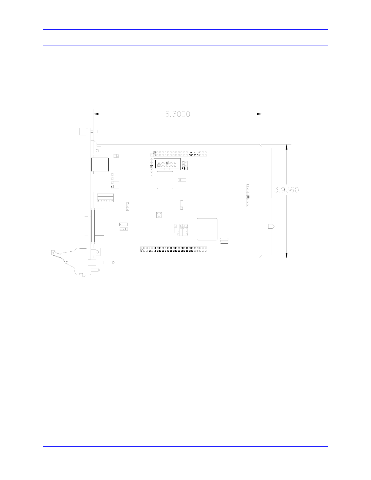
BOARD LAYOUT
This diagram of the Compact UMAC Turbo CPU board shows the locations of the jumpers and
connectors. Detailed information about each of the jumpers and connectors follows.
Current Revision Layout Diagram (rev 103 and above)
E0
E19
J3
E18D
E18C
RP1
RP3
RP2
E18B
E18A
E17
J7
J4
E18
E1A
E11
E1B
J10
E25A
E25B
E25C
J5
W1
E3E4E2
E5
E23
E21
E22
E20
J11
J6
F2
F1
J12
Current UMAC CPCI Turbo CPU Board Layout (rev 103 and above)
J2
J1
Board Layout 9
Page 16

UMAC-CPCI Turbo CPU Board Hardware Reference Manual
Legacy Revision Layout Diagram (rev 102 and below)
10 Board Layout
Page 17

UMAC-CPCI Turbo CPU Board Hardware Reference Manual
JUMPER DESCRIPTIONS
Note:
Pin 1 of an E-point is masked by an X and a bold square in white ink on the composite
side, and by a square solder pad on the solder side.
E0: Reset-Lock Enable (Factory Use Only)
E Point and
Location Description Default
Physical Layout
Jump pins 1 and 2 to lock the Compact UMAC Turbo CPU board
in the reset state to permit installation of on-board logic. This
setting for factory use only.
Remove jumper to permit normal operation of board.
E1A: Servo and Phase Clock Direction Control
E Point and
Physical Layout
Location Description Default
Jump pins 1 and 2 or remove jumper for the Compact UMAC
system to use its internally generated servo and phase clock
signals and to output these signals on the field wiring connector
on the CPU board. E1B should connect pins 2 and 3 or be
removed.
Jump pins 2 and 3 for the Compact UMAC system to expect to
receive its servo and phase clock signals on J2 field-wiring
connector on the Turbo CPU board. E1B should also connect
pins 1 and 2.
E1B: Servo/Phase Clock Source Control
E Point and
Physical Layout
Location Description Default
Jump pin 1 to 2 to get phase and servo clocks from J7 RS422
connector (from an external source such as another UMAC).
Jump pin 2 to 3 to get phase and servo clocks from J1 backplane
connector (from an Acc-24C2x, or equivalent board).
Remove jumper to get phase and servo clocks from J2 Stack
connector (from an Acc-2E or equivalent board)
No jumper installed
Pins 1-2 jumpered
Pins 2 – 3 jumpered
E2: (Reserved for Future Use)
E Point and
Physical Layout
Jumper Descriptions 11
Location Description Default
No jumper installed
Page 18

UMAC-CPCI Turbo CPU Board Hardware Reference Manual
E3: Re-Initialization on Reset Control
E Point and
Location Description Default
Physical Layout
Remove jumper for normal reset mode (default).
Jump pins 1 to 2 for re-initialization on reset.
E4: (Reserved for Future Use)
E Point and
Physical Layout
Location Description Default
No jumper installed
E5: USB/Ethernet Communication Jumper
E Point and
Physical Layout
Location Description Default
Jump 1-2 for CPCI Host Bridge card
Jump 2-3 for Ethernet or USB communications from J7 (Ethernet
connector) or J3 (USB connector).
No jumper installed
Pins 2-3 jumpered
E11: Power Supply Check Control
E Point &
Physical Layout
E11:
Location Description Default
Jump E11 pin 1 to 2 to include the +12V and –12V analog
supplies from the J1 backplane connector in the power-supply
check circuit, inhibiting outputs if these supplies fail.
Remove E11 jumper so only 5V digital supply is used in powersupply check circuit.
E17 – E18: Serial Port Select
E Point and
Physical Layout
E17:
E18:
Location Description Default
Jump E17 pin 1 to 2 to select RS-232 serial data input for main
serial port (J4 front-panel or J2 backside connector).
Jump E17 pin 2 to 3 to select RS-422 serial data input for main
serial port (J4 front-panel or J2 backside connector).
Jump E18 pin 1 to 2 to disable Phase/Servo Clock on J2
Jump E18 pin 2 to 3 to enable Phase/Servo Clock on J2
No jumper installed
Pins 1-2 jumpered
Pins 1-2 jumpered
12 Jumper Descriptions
Page 19

UMAC-CPCI Turbo CPU Board Hardware Reference Manual
E18A, B, C, D: Ethernet Communication Control
E Point and
Location Description Default
Physical Layout
E18D1
E18C1
E18B1
E18A1
Jump 1 to 2 to Ethernet Connection to J7 front connector
Jump 2-3 for Ethernet connection through back J2 connector
E19: Watchdog Disable Jumper
E Point and
Physical Layout
Location Description Default
Jump pin 1 to 2 to disable Watchdog timer (for test purposes
only.).
Remove jumper to enable Watchdog timer.
E20 – E22: Power-Up/Reset Load Source
E Point and
Physical Layout
E20:
Location Description Default
To load active memory from flash IC on power-up/reset,
Remove jumper E20;
Jump E21 pin 1 to 2;
Jump E22 pin 1 to 2.
Other combinations are for factory use only; the board will not
operate in any other configuration.
Pins 1-2 jumpered
No jumper installed
No E20 jumper
installed
E21 and E22 jump pin
1 to 2
E23: Firmware Reload Enable
E Point and
Physical Layout
Location Description Default
Jump pin 1 to 2 to reload firmware through serial or host bus port.
Remove jumper for normal operations.
E25A, B, C: Flash Memory Firmware Bank Select
E Point and
Physical Layout
Location Description Default
Remove all jumpers to select standard factory-installed bank of
operational firmware.
Install one or more jumper(s) to select alternate bank of operation
firmware to install (E23 ON) or use (E23 OFF).
No jumper installed
No jumpers installed
Jumper Descriptions 13
Page 20

UMAC-CPCI Turbo CPU Board Hardware Reference Manual
W1: Flash IC Power Supply Select Jumper
E Point and
Physical Layout
Location Description Default
B-1
(Note: This jumper is set at the factory and possibly hard soldered.
Users should not change this jumper.)
Jump pin 1 to 2 to select 3.3V supply for flash memory IC in U10.
Jump pin 2 to 3 to select 5V supply for flash memory IC in U10.
Setting dependent on
flash IC used.
14 Jumper Descriptions
Page 21

UMAC-CPCI Turbo CPU Board Hardware Reference Manual
CONNECTOR SUMMARY
J1: *
J2: *
J4: *
J5:
J6:
J10:
J11:
J11A:
J12:
J12A:
* Pinouts are shown in the next section. Connectors not flagged with an asterisk are for internal use or
factory setup.
Compact UBUS Backplane Connector
Thru-Backplane Field Wiring Connector
RS-232 Front-Panel Serial-Port Connector
JTAG/OnCE (for factory use only): 10-pin IDC connector
JISP (for factory use only): 8-pin SIP connector
JISP_B (for factory use only) 8-pin SIP connector
First component-side stack connector to CPCI bridge board
First solder-side stack connector to CPCI bridge board
First component-side stack connector to CPCI bridge board
First solder-side stack connector to CPCI bridge board
Connector Summary 15
Page 22

UMAC-CPCI Turbo CPU Board Hardware Reference Manual
16 Connector Summary
Page 23

UMAC-CPCI Turbo CPU Board Hardware Reference Manual
CONNECTOR PINOUTS
Compact UBUS Connector (J1) Pinout
Row Z A B C D E F
25 GND 5V 3.3V 5V GND
24 GND BD02 5V V(I/O) BD01 BD00 GND
23 GND 3.3V BD05 BD04 5V BD03 GND
22 GND BD09 BD08 3.3V BD07 BD06 GND
21 GND 3.3V BD13 BD12 BD11 BD10 GND
20 GND BD17 GND BD16 BD15 BD14 GND
19 GND 3.3V BD20 BD19 GND BD18 GND
18 GND BD23 GND 3.3V BD22 BD21 GND
17 GND 3.3V {BD26} {BD25} GND {BD24} GND
16 GND {BD30} GND {BD29} {BD28} {BD27} GND
15 GND 3.3V BWR- BRD- GND {BD31} GND
14 (KEY) (KEY) (KEY) (KEY) (KEY) (KEY) (KEY)
13 (KEY) (KEY) (KEY) (KEY) (KEY) (KEY) (KEY)
12 (KEY) (KEY) (KEY) (KEY) (KEY) (KEY) (KEY)
11 GND CS10- CS4- CS3- GND CS2- GND
10 GND CS16- GND 3.3V CS14- CS12- GND
9 GND IREQ2- IREQ1- MEMCS1- GND MEMCS0- GND
8 GND PHASE+ GND SERVO+ WAIT- IREQ3- GND
7 GND PHASE- WDO SERVO- GND GND
6 GND BA02 GND 3.3V BA01 BA00 GND
5 GND BA04 BA03 RESET- GND BX/Y GND
4 GND BA07 GND V(I/O) BA06 BA05 GND
3 GND BA11 BA10 BA09 5V BA08 GND
2 GND {BA15} 5V {BA14} BA13 BA12 GND
1 GND 5V -12V PWRGUD +12V 5V GND
Notes:
1. Row 25 is physically at the top of the connector in its “normal” orientation; Row 1 is at the bottom.
Looking from the front of the rack, Column Z is on the left; Column F is on the right.
2. Supply (Vxx & xxV) and ground pins are in the same locations as the Compact PCI bus.
3. Spaces marked (KEY) are for the mechanical key; these are not pins.
4. Pins marked with {} brackets are reserved for future use; the signals inside the brackets are proposed
for future expansion to a 32-bit data bus and 16-bit address bus.
Connector Pinouts 17
Page 24

UMAC-CPCI Turbo CPU Board Hardware Reference Manual
Compact UMAC Turbo CPU Board J2 Connector
Row Z A B C D E F
22 GND +5V GND
21 GND RxD/ CTS +5V TxD/ RTS GND
20 GND RD- RD+ GND SD- SD+ GND
19 GND CS+ CS- GND RS+/ RS- GND
18 GND DSR DTR INIT/ GND
17 GND SERVO- SERVO+ PHASE- PHASE+ GND
16 GND GND
15 GND AuxRxD/ AuxCTS AuxTxD/ AuxRTS GND
14 GND AuxDSR AuxDTR GND
13 GND USBDP (D+) GND USBDM (D-) GND
12 GND GND
11 GND EthTxF+ EthTxF- EthRxF+ EthRxF- GND
10 GND GND
9 GND GND
8 GND GND
7 GND GND
6 GND GND
5 GND GND
4 GND GND
3 GND GND
2 GND WD_NO WD_COM WD_NC GND
1 GND GND
Notes:
1. Row 25 is physically at the top of the connector in its normal orientation; Row 1 is at the bottom. Looking
from the front of the rack, Column Z is on the left; Column F is on the right.
2. The RxD/, CTS, TxD/, and RTS lines are standard RS-232 signals. The inputs are only used if jumpers E17
and E18 each connect their pins 1 and 2. The DSR and DTR lines are simply shorted together.
3. The RD-, RD+, SD-, SD+, CS+, CS-, RS+, and RS- lines are standard RS-422 signals. The inputs are only
used if jumpers E17 and E18 each connect their pins 2 and 3.
4. The SERVO-, SERVO+, PHASE- and PHASE+ clock lines are at RS-422 levels. These signals are outputs if
jumper E1A connects its pins 1 and 2; they are inputs if jumper E1A connects pins 2 and 3.
5. The AuxRxD/, AuxCTS, AuxTxD/, and AuxRTS lines are standard RS-232 signals. These signals are
provided only if the Option 9T auxiliary serial port is ordered. The AuxDSR and AuxDTR lines are simply
shorted together.
6. The USBDP(D+) and USBDM(D-) signals are standard USB signals. They are provided only if the Option
1A USB interface is ordered.
7. The EthTxF+, EthTxF-, EthRxF+, and EthRxF- signals are standard Ethernet signals. They are provided only
if the Option 1 Ethernet interface is ordered.
8. The WD_NO (normally open), WD_COM (common) and WD_NC (normally closed) lines are the outputs of
the watchdog-timer hard-contact relay. The normally open contact is only conducting to common if the card is
powered and operating correctly. The normally closed contact is conducting only to common if the card is not
powered or the watchdog timer has tripped.
18 Connector Pinouts
Page 25
UMAC-CPCI Turbo CPU Board Hardware Reference Manual
J4: RS-232 Serial Port Connector
(DB-9S Connector)
Pin # Symbol Function Description Notes
1 N.C. No connect
2 TXD- Output Send Data Low TRUE
3 RXD- Input Receive Data Low TRUE
4 DSR Bidirect Data Set Ready Shorted to DTR
5 GND Common Compact UMAC Reference
6 DTR Bidirect Data Terminal Ready Shorted to DSR
7 CTS Input Clear to Send High TRUE
8 RTS Output Request to Send High TRUE
9 N.C. No connect
Jumpers E17 and E18 should connect pins 1 and 2 to use this port for RS-232 communications; they should connect pins 2
and 3 to use this port for RS-422 communications.
Connector Pinouts 19
Page 26

UMAC-CPCI Turbo CPU Board Hardware Reference Manual
20 Connector Pinouts
Page 27
UMAC-CPCI Turbo CPU Board Hardware Reference Manual
ACCESSORIES
The Compact UMAC Turbo CPU board is always used with accessory boards. Delta Tau provides
several accessory boards in the Compact UMAC family that can be used with the CPU board; other
parties may produce accessory boards as well. Each accessory board has its own hardware reference
manual.
Acc-Cx Compact UBUS Backplane Boards
The Acc-Cx family of Compact UBUS backplane boards
provides the means for the CPU board to communicate with
other accessory boards. The x in the name of the backplane
board refers to the number of backplane data slots provided.
This picture shows an Acc-C8 8-slot backplane board. It has
a P47-style power connector suitable for a standard 1-slot
CPCI-format power supply.
Acc-8CR Test Breakout Board
The Acc-8CR board provides a behind-the-backplane breakout scheme for the J2 field wiring connector
on any of the 3U-format Compact UMAC board. It is designed to plug into the rear of an Acc-Cx
Compact UBUS backplane board, and it meets the Compact PCI physical specification (100mm x 80mm)
for rear distribution boards. It has 110 screw-down terminal points, one for each signal on the J2 field
wiring connector.
Acc-11C Sinking I/O Board
The Acc-11C board provides 32 isolated 12V-24V
sinking inputs and 16 isolated sinking outputs up to 24V
and 100mA per output. With its Option 1 mezzanine
board, an additional 32 inputs and 16 outputs are
provided, for a total of 96 I/O points in a single slot.
Accessories 21
Page 28

UMAC-CPCI Turbo CPU Board Hardware Reference Manual
Acc-24C2 PWM Axis Board
The Acc-24C2 PWM axis board provides the interface circuitry for four axes of purely digital control in a
single slot, with direct PWM outputs, serial ADC inputs, quadrature encoder inputs, and input/output
flags. Because of pin limitations on the J2 field wiring connector, signals that are differential on other
Acc-24x2 boards are single-ended here. To take these signals any significant distance, differential line
drivers and receivers are required on a distribution board.
Acc-24C2A Analog Axis Board
The Acc-24C2A analog axis board provides the
interface circuitry for four axes of control in a single
slot, with analog interface to the servo drives. It also
has one pulse-and-direction output per axis for stepper
drives, or stepper-replacement servo drives. One 18-bit
D/A converter comes standard for each axis; Option 1
provides a second D/A converter per axis, which can be
used as part of a sine-wave control scheme, or for nonservo use. Option 2 provides eight 12-bit A/D
converters.
Acc-51C Analog Encoder Interpolator Board
The Acc-51C provides the circuitry for the high-resolution interpolation of two or four analog sine/cosine
encoders, yielding 4096 states per line of the encoder. The board comes standard with two channels of
interface; Option 1 provides two additional channels.
22 Accessories
Page 29

UMAC-CPCI Turbo CPU Board Hardware Reference Manual
O
SCHEMATICS
DATA SYSTEMS INC. AND IS LOANED SUBJECT TO RETURN UPON
THIS DOCUMENT IS THE CONFIDENTIAL PROPERTY OF DELTA TAUTHIS DOCUMENT IS THE CONFIDENTIAL PROPERTY OF DELTA TAU
DATA SYSTEMS INC. AND IS LOANED SUBJECT TO RETURN UPON
DEMAND. TITLE TO THIS DOCUMENT IS NEVER SOLD OR
TRANSFERRED FOR ANY REASON. THIS DOCUMENT IS TO BE USED
DEMAND. TITLE TO THIS DOCUMENT IS NEVER SOLD OR
TRANSFERRED FOR ANY REASON. THIS DOCUMENT IS TO BE USED
ONLY PURSUANT TO WRITTEN LICENSE OR WRITTEN INSTRUCTIONS
ONLY PURSUANT TO WRITTEN LICENSE OR WRITTEN INSTRUCTIONS
OF DELTA TAU DATA SYSTEMS INC. ALL RIGHTS TO DESIGNS AND
OF DELTA TAU DATA SYSTEMS INC. ALL RIGHTS TO DESIGNS AND
INVENTIONS ARE RESERVED BY DELTA TAU DATA SYSTEMS INC.
INVENTIONS ARE RESERVED BY DELTA TAU DATA SYSTEMS INC.
POSSESSION OF THIS DOCUMENT INDICATES ACCEPTANCE OF THE
ABOVE AGREEMENT.
POSSESSION OF THIS DOCUMENT INDICATES ACCEPTANCE OF THE
ABOVE AGREEMENT.
+3P3V
(JTAG/OnCE)
J5
J5
TSI
GND
1
2
TSO
GND
3
TCK
GND
4
N.C.
5
6
RST-
TMS
7
+3.3V
N.C.
9
10
11
12
DE-
TRST-
13
14
HEADER14_NO8
J6
(jisp)
+3.3V
J6
SDI
1
SDO
2
3
4
ispEN-
GND
6
MODE
7
SCLK
8
HSIP8NO5
GND
BWR-
BA14
BRD-
FLASHCS-
DRAMCS-
PRAMCS-
DRAMCS-
BA08
FLASHCS-
BA10
PRAMCS-
BA15
ISPEN-
BA11
BA09
A16
A17 CS12-
RESET-
MODE
WR-
C86
+5V
.1UF
GND
C87
.1UF
PRAM MEMORY P:
$040000-$0403FF User Written Phase (1K)
$040400-$040BFF User Written Servo (2K)
$000000-$00FFFF Firmware (64K)
$050000-$05FFFF Plcc Standard Memory Option (64K)
$050000-$0BFFFF Plcc Extended Memory Option (448K)
1
3
2
C21
.01UF
RP4
7
6
5
4
1
3
4
9
10
11
13
14
15
16
17
7
8
19
29
32
31
24
48
6
30
12
18
36
42
ispLSI2032E-135LT48
10
3.3KSIP10C
9
8
PRDY
ISPEN-
TDI
TDO
TCK
TMS
RESET-
DE-
TRST-
A17
ISPEN-
A15
MODE
WR-
U6B
A14
WR
RD
FLASHCS
DRAMCS
PRAMCS
A8
A9
A10
A11
A15
BSCAN
TDI/A16
TDO/A17
TCK
TMS
RESET
VCCIO
VCCIO
VCC
VCC
GND
GND
GND
GND
TURBO-DECODE5
(TQFP48)
BSTD1
BSRD1
BSC12
BTXD
BRTS-
BSCK1
BHREQ-
BSC11
RESET
PRDY
CPURST-
IOCS_A
IOCS_B
DPRCS0
DPRCS1
VMECS0
VMECS1
IOCS
CS00
CS02
CS04
CS06
CS10
CS12
CS14
CS16
N.C.
N.C.
CS0
CS1
CS2
CS3
CS4
C24
.1UF
GND
2
20
21
22
23
25
26
27
28
33
34
35
37
44
45
46
47
38
39
40
41
5
43
U34
2
A0
3
A1
4
A2
5
A3
6
A4
7
A5
8
A6
9
A7
1
T/R
19
OE
PI74FCT245TL
(TSSOP20)
+3P3V
C22
.1UF
+3P3V
.1UF
C25
.1UF
C23
GUARD BAND
+3P3V
B0
B1
B2
B3
B4
B5
B6
B7
VCC
GND
+3P3V
IOCS-
A19X/YP
18
17
16
15
14
13
12
11
20
10
A0
A1
A4
A7
A8
A9
A12
OSC_OUT
HACK-
WR-
RD-
BA06
BA07
BA09
BA13
BA12
BA14
BA15
CPURST-
3
TRST-
EN-B,D
SIRQ-
OUT-B
OUT-B
OUT-D
OUT-D
WD
BBRCS-
1
2
3
4
5
6
7
8
ECS-36-20-5P
3.6864Mhz
C113
.1UF
OUT-B
EN-B,D
OUT-D
VCC
IN-B
N.C.
IN-D
R5
1K
TP7
SIRQ-
U43
DIN
DOUT
SCLK
CS
N.C.
IRQ
SHDN
GND X2
MAX3100CEE
(QSOP)
SOCKET REQ'D
+5V
1
3.3K
5
RP2C
5
RX
+5V
+5V
16
VCC
15
IN-B
14
IN-B
13
12
11
10
IN-D
9
C100
20
.1UF
19
18
17
16
15
14
13
12
11
C101
.1UF
NMI-
D1
LED
RED
PWR
BBRCS-
RESET-
BBRAMCS-
+3P3V
C32
.1UF
16
VCC
15
TX
14
RX
13
RTS
12
N.C.
11
CTS
10
X1
9
Y2
1
RP1A
RP3D
3.3K
2
GND
RP2A
2
6
RESET
RESET
NMI-
1
RX
RTS-
WDO
WDO
E1B 2 TO 3 OFF = DISABLE `PHASE & SERVO' FROM `P1'
R6
1K
RESET-
|Link
|625-0SH3.sch
C99
.1UF
C97
16
C95
U28
.1UF
2
V-
+V
.1UF
C96
.1UF
C93
C94
22pf
22pf
1
1
RP3E
3.3K
RP3A
3.3K
6
2
JUMP 1 TO 2 TO ENABLE "RS232" TRANSCEIVER
E17
RXD
CTS-
TXD
RTS-
RXEN-
9
8
7
6
5
4
RP25
10
1KSIP10C
RT. angle through
PHASE-
E1B 2 TO 1 OFF = DISABLE `PHASE & SERVO' FROM `P2'
E1A 2 TO 3 = DISABLE `CARD0'
NOTE:
E1B 2 TO 3 ON = ENABLE `PHASE & SERVO' FROM `P1'
E1B EMPTY = ENABLE `PHASE & SERVO' FROM `J12/J12A'
|625-0SH2.sch
VCC
1
C2+
C1+
3
C2-
AuxTxD-
C1-
11
TXD
TXD
12
AuxRTS
RXD
RXD
10
RTS
RTS
9
CTS
CTS
VSS
MAX3232ECWE
15
(SOL16)
R15
R14
15K
15K
JUMP 2 TO 3 TO ENABLE "RS422" TRANSCEIVER
JUMP 1 TO 2 TO DIS PHASE,SERVO,INIT ON `J2'
JUMP 2 TO 3 TO ENA PHASE,SERVO,INIT ON `J2'
E18
+5V
3
17
U29
1
3
V-
+V
VCC
C102
2
C2+
C1+
4
C2-
C1-
.1UF
12
C103
TXD
TXD
13
RXD
RXD
.1UF
11
RTS
RTS
TXD
RXD
10
CTS
CTS
1
TXEN
RXEN
CTS-
VSS
LTC1384CS
16
(SOL18)
3
2
ENA422
1
GND
Front Panel
MainRxD-
MainRTS
SERVO-
SERVO+
PHASE+
E1A 2 TO 1 = ENABLE `CARD0'
E1B 2 TO 1 ON = ENABLE `PHASE & SERVO' FROM `P2'
Title
UMAC-CPCI-CPU, DSP56309 CPU SECTI
Size Document Number Rev
D
Date: Sheet
6
C98
4
.1UF
5
AuxTxD-
14
13
AuxRxD-
7
422_RS-
3
E17
1
E18
7
5
6
15
14
8
9
18
R_PHASE+
1
3
5
7
33SIP8I
8
MainCTS
RP15
2
MainRTS
2
10
9
CHGND
R_PHASE-
422_CS+
422_RS+
74ACT08
(SO14)
(JRS232)
GND
2
4
6
8
422_SD+
422_SD-
422_SD+
U38C
J4
MainTxD-
422_RD-
422_CS-
422_RS-
N.C.
R_PHASE-
R_PHASE+
422_RD+
422_RD-
GND
MainRTS
MainDSR
MainCTS
SHEET3
625-0SH3
AuxCTS
422_RD+
MainTxD-
8
GND
Delta Tau Data Systems, Inc.
603625-322A
AuxRxD-
C106
.1UF
MainCTS
R_SERVO-
R_SERVO+
AuxCTS
C105
.1UF
422_SD-
422_CS-
MainRxD-
N.C.
AuxRTS
C104
.1UF
422_CS+
422_RS+
MainTxD-
1
6
2
MainRTS
7
3
8
4
9
5
R_SERVO+
J4
DB9F
10
SHEET2
625-0SH2
13Monday, January 14, 2002
MainRxD-
MainCTS
MainDTR
MainTXD-
MainRXD-
R_SERVO-
of
-
+5V
+3P3V
C14
+
C39
+
10UF
(TANT)
U7
48
OE1
47
A0
46
A1
45
GND
A3
44
A2
A2
43
A3
42
VCC
41
A4
40
A5
A5
39
GND
A6
38
A6
37
A7
36
A8
35
A9
34
GND
A10
33
A10
A11
32
A11
31
VCC
A13
30
A12
29
A13
28
GND
A15
27
A14
A14
26
A15
25
OE2
74LCX16245
U8
(TSSOP48)
48
OE1
47
A0
46
A1
45
GND
44
A2
43
A3
42
VCC
41
A4
40
BA05
A5
39
GND
38
A6
37
A7
36
A8
35
A9
BA08
34
GND
33
A10
32
A11
BA10
31
VCC
BA11
30
A12
29
A13
28
GND
27
A14
26
A15
25
OE2
74LCX16245
(TSSOP48)
C151
.1UF
C150
48
47
46
45
.1UF
44
43
42
41
40
39
38
37
36
35
34
33
32
31
30
29
28
PWRG
+5V
27
26
25
PI74FCT16245ATA
PWRG
GND
F1ER
9
8
7
6
5
4
3
2
C88
10
1
GND
.1UF
16V
T/R1
GND
VCC
GND
GND
B10
B11
VCC
B12
B13
GND
B14
B15
T/R2
T/R1
B0
B1
GND
B2
B3
VCC
B4
B5
GND
B6
B7
B8
B9
GND
B10
B11
VCC
B12
B13
GND
B14
B15
T/R2
U51
OE1
A0
A1
GND
A2
A3
VCC
A4
A5
GND
A6
A7
A8
A9
GND
A10
A11
VCC
A12
A13
GND
A14
A15
OE2
(TSSOP48)
BFUL
TXD
RP14
3.3KSIP10C
B0
B1
B2
B3
B4
B5
B6
B7
B8
B9
HREQ-
GND
BA08
BA11
BA13
BHACK-
1
2
3
4
5
6
7
8
9
10
BA08_A
11
12
13
14
15
16
17
18
19
20
21
22
23
24
EROR
ENA422
10UF
16V
(TANT)
GND
1
BA00
2
BA01
3
BA02
4
5
6
BA04
7
8
BA05
BA06
9
10
11
BA09
12
BA07
13
BA10
14
15
16
17
BA12
18
19
BA14
20
21
22
BA15
23
24
EXTAL
BX/Y
BWR-
BRD-
BA07_A
BA06_A
BA10_A
BA09_A
BA11_A
BA13_A
BA12_A
BA14_A
C152
.1UF
+5V
T/R1
B0
B1
GND
B2
B3
VCC
B4
B5
GND
B6
B7
B8
B9
GND
B10
B11
VCC
B12
B13
GND
B14
B15
T/R2
IPOS
IPOS
RTS-
BA03
BA05_A
1
4
7
10
13
14
15
16
17
18
19
20
21
22
23
24
+3P3V
BA00
BA01
BA03
+3P3V
BA02
BA04
BA05
BA06
BA07
BA08
BA09
BA10
+3P3V
BA11
BA13
BA12
BA14
+3P3V
BA15
+3P3V
GUARD BAND
BX/Y
+3P3V
C27
BWR-
.1UF
BRD-
BA05_A
BA06_A
BA08_A
BA10_A
BA07_A
C26
+3P3V
BA09_A
BA11_A
.1UF
BA12_A
BA13_A
BA14_A
+3P3V
GND
+3P3V
C40
5
U9
WAIT2-
WAIT2-
WAIT1-
C153
CS0-
.1UF
PWRGUD
GND
CS02-
MEMCS0-
IOCS_B-
DPRCS0-
CS00-
CS04-
CS06-
MEMCS1-
CS2-
CS3-
CS10-
IOCS_A-
VMECS0-
CS0-
CS1-
CS00-
CS1-
CS2-
CS3-
CS04-
CS02-
CS10-
CS06-
CS12-
CS14-
CS16-
CS16-
PWRGUD
CS14-
CS4-
CS4-
MEMCS1-
MEMCS0-
IOCS_B-
VMECS0-
IOCS_A-
DPRCS0-
2
3
5
6
8
9
11
12
EROR
BFUL
F1ER
HREQ-
1
4
.1UF
2
WAIT1-
NC7SZ00
3
(SOT23-5)
GND
X/Y:$078200-$0782FF
X/Y:$078100-$0781FF
X/Y:$078300-$0783FF
X/Y:$078000-$0780FF
X/Y:$078B00-$078BFF
X/Y:$078C00-$078CFF
X/Y:$078800-$0789FF
X/Y:$078A00-$078AFF
X/Y:$078D00-$078DFF
X/Y:$078E00-$078EFF
X/Y:$078F00-$078FFF
X/Y:$078400-$0787FF
X/Y:$068000-$06FFFF EXTENDED MEMORY OFF_BOARD (32K)
X/Y:$074000-$077FFF
X/Y:$070000-$073FFF
X/Y:$060000-$067FFF EXTENDED MEMORY ON_BOARD (32K)
TA-
GND
1
PHA_A
2
BCTS-
BRXD
BHA1
MODD/IRQD-
RESET
1
+5V
8
7
6
5
4
3
2
U33A
2
1
74ACT14
(SO14)
5
13
4
+5V
3
GND
PHASE
SERVO
SERVO
RESET-
CPURST-
WAIT1-
WAIT2-
PHASE
3.3KSIP10C
RXD
CTS-
RP13
IRQB-
NC7SZ08M5
(SOT23-5)
SER_A
BHA2
BHA0
HACK-
T/R-
+5V
10
9
U50
1
2
3
U33F
74ACT14
(SO14)
OSC_OUT
U4F
13
(SO14)
74ACT14
10
RP20
U27
3.3KSIP10C
2
A0
3
A1
4
A2
9
8
7
6
5
4
5
A3
6
A4
7
A5
8
A6
9
A7
1
T/R
19
OE
74LCX245
(TSSOP20)
U33E
11
74ACT14
(SO14)
12
19.6608Mhz
R1
19.6608Mhz
12
10
ENA_P2-
ENA_P2-
RESET
ENA_P1-
CARD0
PHA
SER
R3
10K
5
RP12C
1KSIP6I
6
2
E19
1
D5
3
Vout
+
C16
.1UF
C17
D6
1
C36
.1UF
U4A
GND
+5V
2
1
74ACT14
(SO14)
GND
1
3
2
Q1
MMBT3906LT1
(SOT23)
R4
C34
+
100K
1UF
35V
tant
"Vbat" s/b 30mil trace
Vbat
Q3
3
MMBT3906LT1
1
Vout
(SOT23)
3
C1
.1UF
C35
.01UF
2
R2
1K
INIT-
+3P3V
18
B0
17
B1
16
B2
15
B3
14
IRQB-
B4
13
B5
12
B6
11
B7
20
VCC
10
GND
C92
.1UF
U33B
4
3
10
74ACT14
(SO14)
RESET_A
U33D
9
74ACT14
(SO14)
INIT-
WDTC
RXD
BSA02
CTS-
BSER
BSA00
BPHA
BSA02
BSA01
BSA01
BSA00
IRQB-
JUMP `E0'
C111
.1UF
GND
GND
BPHA
BSER
RESET_A
8
`isp' PART
R7
100
+3P3V
3.6V BAT
TO LOAD
BT1
.01FARAD
FM0H103Z
2
E0
1
MMBD301LT1
NEC
1
MMBD301LT1
PHA
SER
+5V
1
1KSIP6I
U2
1
VOUT
2
VCC RST
3
ON
4
GND CEI
MAX795SCSE
(SO8)
ENA_P1-
1
RP12A
MMBD301LT1
.1UF
CARD0
4
5
74ACT08
U4B
3
74ACT14
D3
2
1
2
3
4
5
6
7
8
MMBD301LT1
BATT
CEO
C15
3.3KSIP8I
2
U38B
(SO14)
U3
N.C.
IN
N.C.
MODE
N.C.
TOL
N.C.
GND
DS1231S
(SOL16)
1
1
E1B
(SO14)
RP10A
7
3.3KSIP8I
(SOT23)
3
3
1KSIP6I
D4
8
7
6
5
RP10D
1
3
4
2N7002
RP12B
3
3.3KSIP8I
3
SOT23
2
RP11B
6
3
+5V
8
1
3.3KSIP8I
GND
Q4
N.C.
VCC
N.C.
N.C.
RST
N.C.
RST
3
SOT23
RP11A
4
NMI
3.3KSIP8I
3.3KSIP8I
1
2
GND
PHASE+
3
4
SERVO-
5
ENA422
PHASE+
1
2
RP10B
3.3KSIP8I
RP11C
5
16
15
14
13
12
11
10
9
5
2
.1UF
Q2
2N7002
(SOT23)
RP10C
3.3KSIP8I
PHASE-
U33C
74ACT14
SERVO-
(SO14)
1
3
PHASE+
PHASE-
SERVO-
C2
7
E1A
SERVO+
4
6
RP11D
+5V
11
SERVO+
6
6
2
8
1
2
U4E
74ACT14
SERVO+
SOT23
2N7002
(SOT23)
(SO14)
5
Q5
3
PHASE-
1
6
3.3K
10
RP1E
U4C
74ACT14
R10
STD0
SCK0
SC02
GND
U38A
1
(SO14)
2
74ACT08
U31
1
IN-A
2
OUT-A
3
N.C.
4
OUT-A
5
EN-A,C
6
OUT-C
7
N.C.
8
OUT-C N.C.
9
IN-C
10
GND
MC75174BDW
(SOL20)
GND
6
(SO14)
U4D
9
74ACT14
1K
SRD0
GND
1
RP1D
3.3K
5
GND
U30
1
IN-A
2
IN-A
3
OUT-A
4
EN-A,C
5
OUT-C
6
IN-C
7
IB-C
8
GND IN-D
MC3486D
(SO16)
8
(SO14)
D2
LED
GRN
Schematics 23
Page 30

THIS DOCUMENT IS THE CONFIDENTIAL PROPERTY OF DELTA TAU
O
DATA SYSTEMS INC. AND IS LOANED SUBJECT TO RETURN UPON
DEMAND. TITLE TO THIS DOCUMENT IS NEVER SOLD OR
TRANSFERRED FOR ANY REASON. THIS DOCUMENT IS TO BE USED
ONLY PURSUANT TO WRITTEN LICENSE OR WRITTEN INSTRUCTIONS
OF DELTA TAU DATA SYSTEMS INC. ALL RIGHTS TO DESIGNS AND
INVENTIONS ARE RESERVED BY DELTA TAU DATA SYSTEMS INC.
POSSESSION OF THIS DOCUMENT INDICATES ACCEPTANCE OF THE
ABOVE AGREEMENT.
J1
J1-1
{BA15}
PHASE-
PHASE+
IREQ2-
CS16-
CS10-
+3.3V
{BD30}
+3.3V
+3.3V
+3.3V
+3.3V
IREQ1-
{BD26}
{BD20}
PWRGUD
{BA14}
V(I/O
RESET-
SERVO+
SERVO-
MEMCS1-
{BA29}
{BA25}
V(I/O)
(KEY)
(KEY)
(KEY)
{BA28}
+3.3V
IREQ3-
MEMCS0-
(KEY)
(KEY)
(KEY)
{BD31}
{BD24}
{BD27}
BA07
(KEY)
BD17
(KEY)
BWR-
(KEY)
(KEY)
+3.3V
BD16
BD12
BD04
+12V
BD11
BD07
CS12-
BD10
BD03
BA11
BA04
BA02
BD09
BD02
-12V
BA03
CS4-
(KEY)
(KEY)
BD08
BD05
N.C.
BA09
+3.3V
BRD-
BD19
+3.3V
BA13
BA06
WAIT-
DB22
BD15
BD01
BA05
BA00
N.C.
CS2-
BD21
BD18
BD14
BD06
BD00
(KEY)
(KEY)
BD23
BA10
BD13
+3.3V
CS3-
(KEY)
N.C.
BA01
CS14-
BA12
BA08
BX/Y
+5V
GND
GND
GND
GND
+5V
+5V
GND
n.c.
GND
n.c.
+5V
+5V
GND
GND
WDO
GND
GND
GND
GND
+5V
+5V
GND
GND
GND
GND
+5V
GND
n.c.
n.c.
GND
GND
n.c.
n.c.
GND
n.c.
GND
GND
n.c.
GND
n.c.
n.c.
GND
n.c.
GND
GND
GND
n.c.
n.c.
A1
A2
A3
A4
A5
A6
A7
A8
A9
A10
A11
A12
A13
A14
A15
A16
A17
A18
A19
A20
A21
A22
A23
A24
A25
CONN175-CPCI
J1-2
B1
B2
B3
B4
B5
B6
B7
B8
B9
B10
B11
B12
B13
B14
B15
B16
B17
B18
B19
B20
B21
B22
B23
B24
B25
CONN175-CPCI
J1-3
C1
C2
C3
C4
C5
C6
C7
C8
C9
C10
C11
C12
C13
C14
C15
C16
C17
C18
C19
C20
C21
C22
C23
C24
C25
CONN175-CPCI
J1-4
D1
D2
D3
D4
D5
D6
D7
D8
D9
D10
D11
D12
D13
D14
D15
D16
D17
D18
D19
D20
D21
D22
D23
D24
D25
CONN175-CPCI
J1-5
E1
E2
E3
E4
E5
E6
E7
E8
E9
E10
E11
E12
E13
E14
E15
E16
E17
E18
E19
E20
E21
E22
E23
E24
E25
CONN175-CPCI
J1-6
F1
F2
F3
F4
F5
F6
F7
F8
F9
F10
F11
F12
F13
F14
F15
F16
F17
F18
F19
F20
F21
F22
F23
F24
F25
CONN175-CPCI
A1
A2
A3
A4
A5
A6
A7
A8
A9
A10
A11
A12
A13
A14
A15
A16
A17
A18
A19
A20
A21
A22
A23
A24
A25
B1
B2
B3
B4
B5
B6
B7
B8
B9
B10
B11
B12
B13
B14
B15
B16
B17
B18
B19
B20
B21
B22
B23
B24
B25
C1
C2
C3
C4
C5
C6
C7
C8
C9
C10
C11
C12
C13
C14
C15
C16
C17
C18
C19
C20
C21
C22
C23
C24
C25
D1
D2
D3
D4
D5
D6
D7
D8
D9
D10
D11
D12
D13
D14
D15
D16
D17
D18
D19
D20
D21
D22
D23
D24
D25
E1
E2
E3
E4
E5
E6
E7
E8
E9
E10
E11
E12
E13
E14
E15
E16
E17
E18
E19
E20
E21
E22
E23
E24
E25
F1
F2
F3
F4
F5
F6
F7
F8
F9
F10
F11
F12
F13
F14
F15
F16
F17
F18
F19
F20
F21
F22
F23
F24
F25
BA11_B
BA07_B
BA04_B
BA02_B
PHASE_B-
PHASE_B+
IREQ2-
CS16-
CS10-
BD23_B
BD17_B
BD09_B
BD02_B
BA10_B
BA03_B
WDO_B
IREQ1-
CS4-
BWR_B-
BD20_B
BD13_B
BD08_B
BD05_B
PWRGUD
BA09_B
V_I/O
RESET_B
SERVO_B+
SERVO_B-
MEMCS1-
CS3-
BRD_B-
BD19_B
BD16_B
BD12_B
BD04_B
V_I/O
BA13_B
BA06_B
BA01_B
WAIT2-
CS14-
BD22_B
BD15_B
BD11_B
BD07_B
BD01_B
BA12_B
BA05_B
BA08_B
BA00_B
BX/Y_B
IREQ3-
MEMCS0-
CS12-
CS2-
BD21_B
BD14_B
BD18_B
BD10_B
BD06_B
BD03_B
BD00_B
GND
CS16-
CS10-
+5V
EQU_1-
+3P3V
+3P3V
+3P3V
+3P3V
+3P3V
+5V
-12V
+5V
GND
GND
GND
IRQB-
GND
GND
GND
GND
+5V
+3P3V
+3P3V
+3P3V
+3P3V
+12V
+5V
GND
GND
GND
GND
GND
GND
GND
+5V
+3P3V
+5V
EQU_2-
+5V
EQU_1-
IRQB-
CS4-
PWRGUD
MEMCS1-
CS3-
WAIT2-
CS14-
EQU_2-
CS12-
MEMCS0-
CS2-
UMAC-CPCI Turbo CPU Board Hardware Reference Manual
(JEXP_A)
J11
BD00_A
BD00_A
BD02_A
BD02_A
BD04_A
BD04_A
BD06_A
BD06_A
BD08_A
BD08_A
BD10_A
BD10_A
BD12_A
BD12_A
BD14_A
BD14_A
BD16_A
BD18_A
BD20_A
BD22_A
BA00_A
BA00_A
BA04_A
BA08_A
BA10_A
BA12_A
BA06_A
BA10_A
BA12_A
BA02_A
BA08_A
BA04_A
BX/Y_A
BA02_A
BA06_A
BX/Y_A
SSM-120-L-DV-LC
HPBD2
HPBD6
BSA00
CPCIDPR-
CS0-
BWR_A-
RESET_A
BD00_A
BD04_A
BD12_A
BD18_A
BD20_A
BA00_A
BA02_A
BA04_A
BA06_A
BA08_A
BA10_A
HPBD0
HPBD2
CPCIDPR-
CS00-
CS0-
BWR_A-
19.6608Mhz
BSA02
CS04-
PWRG
BD22_A
BA12_A
BSA00
SERVO
PWRG
(JEXP_B)
SERVO
BSA02
BD02_A
BD10_A
BD14_A
BX/Y_A
SOLDER SIDE
DIRECTLY UNDER J11
HPBD4
HPBD6
RESET_A
SCL
SOLDER SIDE
DIRECTLY UNDER J12
Title
Size Document Number Rev
Date: Sheet
+5V
HPBD0
GND
HPBD0
HPBD2
HPBD4
HPBD4
HR/W
HPBD6
HR/W
BSA00
CS00-
CPCIDPR-
CS00-
CS04-
CS0-
BWR_A-
RESET_A
19.6608Mhz
19.6608Mhz
PWRG
SCL
BSA02
SCL
GND
+5V
SSM-125-L-DV-LC
+12V
BD06_A
BD08_A
BD16_A
HW20-09-GD-450-SM
+5V
C82
.1UF
U25
1
8
RO
PHA
SERVO
SER
ENA_P1-
PHASE
PHA
R9 100
PHASE
SERVO
R19 100
SER
ENA_P1-
R18 3.3K
GND
IOCS_B-
+3P3V
+3P3V
+3P3V
+3P3V
IOCS_B-
D5
D6
D9
D22
BA02
BA05
D0
D1
D7
D13
D16
D21
D23
BA01
BA04
D2
D3
D4
D8
D10
D11
D12
D14
D15
D17
D18
D19
D20
BA00
BA03
BX/Y
U22
48
OE1
47
A0
46
A1
45
GND
44
A2
43
A3
42
VCCA
41
A4
40
A5
39
GND
38
A6
37
A7
36
A8
35
A9
34
GND
33
A10
32
A11
31
VCCA
30
A12
29
A13
28
GND
27
A14
26
A15
25
OE2
IDT74FCT164245TPA
U23
(TSSOP48)
48
OE1
47
A0
46
A1
45
GND
44
A2
43
A3
42
VCCA
41
A4
40
A5
39
GND
38
A6
37
A7
36
A8
35
A9
34
GND
33
A10
32
A11
31
VCCA
30
A12
29
A13
28
GND
27
A14
26
A15
25
OE2
IDT74FCT164245TPA
(TSSOP48)
BD00_B
BRD-
1
T/R1
2
BD01_B
B0
3
B1
GND
B2
B3
VCCB
B4
B5
GND
B6
B7
B8
B9
GND
B10
B11
VCCB
B12
B13
GND
B14
B15
T/R2
1
T/R1
2
B0
3
B1
4
GND
5
B2
6
B3
7
VCCB
8
B4
9
B5
10
GND
11
B6
12
B7
13
B8
14
B9
15
GND
16
B10
17
B11
18
VCCB
19
B12
20
B13
21
GND
22
B14
23
B15
24
T/R2
+5V
4
BD02_B
BD03_B
5
6
7
8
9
10
11
12
13
14
BD10_B
15
16
17
BD12_B
18
19
20
21
BD15_B
22
23
24
BD19_B
BA03_B
BD04_B
BD05_B
BD06_B
BD07_B
BD08_B
BD09_B
BD13_B
BD14_B
BRD-
BRD-
BD16_B
BD18_B
BD22_B
BD23_B
BA00_B
BA01_B
BA05_B
BX/Y_B
BD11_B
BD17_B
BD20_B
BD21_B
BA02_B
BA04_B
C74
.1UF
+5V
C75
.1UF
+5V
C76
.1UF
+5V
C77
.1UF
+5V
GND
D1
D2
D4
D6
D7
D9
D10
D12
D15
D16
D17
D18
D19
D20
D22
D23
BA00
BA01
BA03
BA12
BA13
D0
D5
BA02
U20
48
OE1
47
A0
46
A1
45
GND
44
A2
43
A3
42
VCCA
41
A4
40
A5
39
GND
38
A6
37
A7
36
A8
35
A9
34
GND
33
A10
32
A11
31
VCCA
30
A12
29
A13
28
GND
27
A14
26
A15
25
OE2
IDT74FCT164245TPA
(TSSOP48)
U21
48
OE1
47
A0
46
A1
45
GND
44
A2
43
A3
42
VCCA
41
A4
40
A5
39
GND
38
A6
37
A7
36
A8
35
A9
34
GND
33
A10
32
A11
31
VCCA
30
A12
29
A13
28
GND
27
A14
26
A15
25
OE2
IDT74FCT164245TPA
(TSSOP48)
U52
2
A0
3
A1
4
A2
5
A3
6
A4
7
A5
8
A6
9
A7
1
T/R
19
OE
PI74FCT245TL
(TSSOP20)
IOCS_A-
IOCS_A-
D3
+3P3V
C45
.1UF
D8
D11
+3P3V
C46
D13
.1UF
D14
+3P3V
C47
D21
.1UF
+3P3V
C48
BA04
BX/Y
.1UF
GND
BA07
BA06
BA09
BA08
BA11
BA10
WDO
RESET_A
BRD-
1
BD00_A
T/R1
2
B0
3
BD01_A
B1
4
GND
5
B2
6
B3
7
VCCB
8
B4
9
B5
10
GND
11
B6
12
B7
13
B8
14
B9
15
GND
16
B10
17
B11
18
VCCB
19
B12
20
B13
21
GND
22
B14
23
B15
24
T/R2
1
T/R1
2
B0
3
B1
4
GND
5
B2
6
B3
7
VCCB
8
B4
9
B5
10
GND
11
B6
12
B7
13
B8
14
B9
15
GND
16
B10
17
B11
18
VCCB
19
B12
20
B13
21
GND
22
B14
23
B15
24
T/R2
+5V
18
B0
17
B1
16
B2
15
B3
14
B4
13
B5
12
B6
11
B7
20
VCC
10
GND
GND
BD04_A
BD05_A
BD11_A
BD15_A
BRD-
BD17_A
BD18_A
BD19_A
BD22_A
BA01_A
BX/Y_A
BA13_B
BD02_A
BD03_A
BD08_A
BD09_A
BD10_A
BD14_A
BD21_A
BD23_A
BA02_A
BA03_A
BA04_A
BD06_A
BD07_A
BD12_A
BD13_A
BRD-
BD16_A
BD20_A
BA00_A
BA12_B
BA06_B
BA07_B
BA09_B
BA08_B
BA10_B
BA11_B
WDO_B
RESET_B
C127
.1UF
+5V
C52
.1UF
C51
+5V
.1UF
+5V
C50
.1UF
+5V
C49
.1UF
+5V
GND
2
RE
3
DE
4
DI GND
ADM1485JR
(SO8)
1
2
3
4
ADM1485JR
VCC
7
B
6
A
5
U26
RO
RE
DE
DI GND
(SO8)
PHASE_B-
PHASE_B+
8
VCC
7
B
6
A
5
C83
.1UF
GND
SERVO_B-
SERVO_B+
HW25-09-GD-450-SM
+5V
GND
HR/W
CS04-
GND
+5V
+12V
BD01_A
12
34
56
78
910
11 12
13 14
15 16
17 18
19 20
21 22
23 24
25 26
27 28
29 30
31 32
33 34
35 36
37 38
39 40
HEADER 20X2(FEM)
CLS120LDDV
J12
12
34
56
78
910
11 12
13 14
15 16
17 18
19 20
21 22
23 24
25 26
27 28
29 30
31 32
33 34
35 36
37 38
39 40
41 42
43 44
45 46
47 48
49 50
HEADER 25X2(FEM)
CLS125LDDV
(JEXP_A)
J11A
12
34
56
78
910
11 12
13 14
15 16
17 18
19 20
21 22
23 24
25 26
27 28
29 30
31 32
33 34
35 36
37 38
39 40
HEADER 20X2(MALE)
HW2015GD450SM
(JEXP_B)
J12A
12
34
56
78
910
11 12
13 14
15 16
17 18
19 20
21 22
23 24
25 26
27 28
29 30
31 32
33 34
35 36
37 38
39 40
41 42
43 44
45 46
47 48
49 50
HEADER 25X2(MALE)
HW2515GD450SM
CS1-
BD05_A
BD07_A
BD15_A
BA11_A
HPBD5
CS06-
INIT-
BD01_A
BD11_A
WAIT2-
BA07_A
VMECS0-
CS02-
BRD_A-
SDA
BD03_A
BA07_A
HPBD7
VMECS0-
PHASE
INIT-
BD21_A
BA05_A
BA09_A
HPBD1
BSA01
BD19_A
BA03_A
BA09_A
BA13_A
HPBD5
BRD_A-
WDO
BD17_A
BA03_A
BA13_A
PHASE
BD09_A
BD13_A
BD15_A
BD23_A
BA11_A
HPBD3
SDA
BD19_A
BD23_A
BA01_A
BD17_A
HPBD1
HDS-
BSA01
CS02-
CS06-
BD03_A
BD09_A
BD11_A
BD13_A
WAIT2-
HPBD3
HPBD7
HDS-
CS1-
WDO
BD05_A
BD07_A
BD21_A
BA01_A
BA05_A
HPBD7
BD05_A
BD09_A
HDS-
WDO
GND
-12V
-5V
BD07_A
BD15_A
BA01_A
BA13_A
HPBD1
HPBD5
CS06-
CS1-
BD03_A
BD11_A
BA03_A
BA05_A
BA07_A
BA11_A
+5V
HPBD3
VMECS0-
BRD_A-
INIT-
SDA
+5V
GND
BD01_A
BD13_A
GND
GND
BA09_A
WAIT2-
JEXP
Modified
BSA01
CS02-
-5V
-12V
WAIT2-
Delta Tau Data Systems, Inc.
UMAC-CPCI-CPU, MEMORY & I/O SECTI
D
603625-322A
23Tuesday, January 15, 2002
of
-
24 Schematics
Page 31

UMAC-CPCI Turbo CPU Board Hardware Reference Manual
o
n
+3P3V
C175
0.1uF
C176
Avcc
+
2.2UF
J3
1
VCC
2
D-
3
D+
4
GND
5
shell
6
USB-B
shell
CHGND
L5
BEAD
C20
0.1uF
GND
OPTION 1
Ethernet Option
CE1
M1
0.1uF
HOLE
M2
CE2
HOLE
0.1uF
M3
CE3
HOLE
0.1uF
M4
CE4
R28
HOLE
0.1uF
1M
CHGND
GND
USBDP
USBDM
1
GND
2
C
3
GND
4
D GND
SN75240PW
GND
U62
8
A
7
GND
6
B
5
GND
R31 1.5K
R30 24.3
R29 24.3
USBRST-
U32
1
2
3
(1-3)(16-14)1:1
4
5
6
7
(6-8)(11-9)1:2.5
8
ST7011
HREQ-
16
15
14
13
12
11
10
9
1:1.41
HOSTENA-
NC7SZ02M5
(SOT32-5)
NC7SZ02M5
(SOT32-5)
ETHENA-
4
4
EthRxF-
EthTxF+
EthRxF+
EthTxF-
+5V
3
D13
MMBD301LT1
(SOT23)
1
1
Q7
2N7002
3
SOT23
2
-5V
+12V
-12V
CARD0
40/60
E_51
TBD_0
XIN_4
ENA_P2-
ENA_P1-
XIN_7
PWRG
TDO_USB
TDI_USB
TMS_USB
TCK_USB
USBD0 HPBD0
USBD1
USBD3
USBD2
USBD4
USBD5
USBD6
USBD7
+3P3
+5V
+12V
-12V
GND
NC7SZ08M5
NC7SZ08M5
J7
10
9
8
7
6
5
4
3
2
1
RJ45
+3P3V
5
U58
1
4
2
3
GND
C160
+3P3V
.1UF
5
U57
1
2
3
GND
RAMCS-
RAMOE-
4
PWRG
NMI-
NMI-
XIN_1
XIN_2
XIN_3
XIN_5
XIN_6
BSC_USB-
+3P3V
5
U54
U65
+3P3V
EQU_1
1
2
NC7SZ00M5
+3P3V
5
1
2
3
GND
5
1
U64
2
3
GND
U73
NC7SZ00
RAMENA-
4
3
GND AuxRxD-
EQU_1
WDO
IPOS
+5V
5
4
3
GND
PSEN-
WDO
USBRD-
+5V
5
U61
1
2
NC7SZ00M5
3
GND
IPOS
1
2
EthExtRxF-
3
2
1
E18A
3
2
1
E18B
3
EthExtTxF-
2
1
E18C
EthExtTxF+
3
2
1
E18D
Q6
3
4
SOT23
EQU_1-
EthExtRxF+
1
2
INIT-
2N7002
U66
1
VREF
2
GND
3
+5V
4
-5V
5
+12V
6
-12V
7
DIN PGND
MAX8215CSD
(SO14)
10
8
9
2
3
4
5
6
7
8
9
1
19
PI74FCT245TL
(TSSOP20)
D9
1SMC5.0AT3
D10
1SMC5.0AT3
D11
1SMC18AT3
D12
1SMC18AT3
U6
A0
A1
A2
A3
A4
A5
A6
A7
T/R
OE
FBR12ND05
6
7
C192
K1
4
9
1
12
VDD
OUT1
OUT2
OUT3
OUT4
DOUT
+5V
1
2
3
4
5
B0
B1
B2
B3
B4
B5
B6
B7
VCC
GND
+
(TANT)
C193
C194
C195
3
5
10
8
RP22
3.3KSIP10C
+5V
18
17
16
15
14
13
12
11
20
10
10UF
16V
+
(TANT)
10UF
9
8
+
(TANT)
25V
14
13
12
11
10
HPBD7
10UF
16V
+
(TANT)
WD_NO
HPBD1
GND
10UF
25V
ENA_P1-
.01UF
HPBD2
HPBD4
WD_COM
WD_NC
REMOVE `E11' FOR
C190
.1UF
GND
CARD0
ENA_P2-
HSIP8NO5
C191
HPBD3
HPBD5
HPBD6
C28
.1UF
(TAB IS INPUT)
(SOT223)
LT1175CST-5
2
+5V
DIGITAL ONLY USE
(jisp_b)
J10
J10
+5V
1
2
3
4
6
7
8
GND
HPBD0
HPBD2
HPBD3
HPBD4
HPBD7
TP1
GND
VI
VR1
1
1
E11
E4
SDI
GND
E11
HPBD5
ispEN-
SCLK
HPBD1
HPBD6
VO
2
E2
E2
E3
E3
E4
GND
+5V
SDO
MODE
GND
+3P3V
TP2
+3P3
+5V
GND
TP5
TP4
-12V
+12V
TP3
+5V
GND
+12V
-12V
TP6
-5V
3
-5V
C196
.1UF
GND
J2
J2-1
A1
A1
A2
A2
A3
A3
A4
A4
A5
A5
A6
A6
A7
A7
A8
A8
A9
A9
A10
R_SERVO-
422_CS+
EthExtTxF-
AuxCTS
EthExtRxF+
MainTxD-
422_RS-
422_RD-
422_CS-
A10
A11
A12
A13
A14
A15
A16
A17
A18
A19
A20
A21
A22
+5V
GND
CONN154-CPCI
D1
D2
D3
D4
D5
D6
D7
D8
D9
D10
D11
D12
D13
D14
D15
D16
D17
D18
D19
D20
D21
D22
A11
A12
A13
A14
A15
A16
A17
A18
A19
A20
A21
A22
J2-2
B1
B1
B2
B2
B3
B3
B4
B4
B5
B5
B6
B6
B7
B7
B8
B8
B9
B9
B10
B10
B11
B11
B12
B12
B13
B13
B14
B14
B15
B15
B16
B16
B17
B17
B18
B18
B19
B19
B20
B20
B21
B21
B22
B22
CONN154-CPCI
C1
C2
C3
C4
C5
C6
C7
C8
C9
C10
C11
C12
C13
C14
C15
C16
C17
C18
C19
C20
C21
C22
GND
J2-4
D1
D2
D3
D4
D5
D6
D7
D8
D9
D10
D11
D12
D13
D14
D15
D16
D17
D18
D19
D20
D21
D22
CONN154-CPCI
J2-5
E1
E1
E2
E2
E3
E3
E4
E4
E5
E5
E6
E6
E7
E7
E8
E8
E9
E9
E10
E10
E11
E11
E12
E12
E13
E13
E14
E14
E15
E15
E16
E16
E17
E17
E18
E18
E19
E19
E20
E20
E21
E21
E22
E22
CONN154-CPCI
J2-6
F1
F2
F3
F4
F5
F6
F7
F8
F9
F10
F11
F12
F13
F14
F15
F16
F17
F18
F19
F20
F21
F22
CONN154-CPCI
EthExtTxF+
AuxDSR
AuxRXD-
SERVO-
MainDSR
422_RD-
MainRXD-
WD_NO
EthExtTxF-
AuxCTS
SERVO+
422_CS-
422_RD+
MainCTS
J2-3
C1
C2
C3
C4
C5
C6
C7
C8
C9
C10
C11
C12
C13
C14
C15
C16
C17
GND
C18
C19
C20
C21
C22
CONN154-CPCI
WD_NC
EthExtRxF+
USBDM
INIT-
422_RS+
AuxRTS
PHASE+
422_SD+
MainRTS
GND
n.c.
F1
F2
n.c.
GND
F3
F4
F5
GND
F6
F7
F8
n.c.
F9
GND
F10
n.c.
F11
GND
F12
n.c.
F13
GND
F14
F15
GND
F16
n.c.
F17
F18
F19
F20
F21
F22
33Tuesday, January 15, 2002
USBDP
+5V
n.c.
GND
PHASE-
GND
GND
of
422_CS+
AuxDTR
MainDTR
GND
+5V
AuxTXD-
422_SD-
MainTXD-
422_RS-
n.c.
n.c.
n.c.
n.c.
GND
WD_COM
GND
EthExtRxF-
EthExtTxF+
AuxRxD-
R_SERVO-
422_CS+
422_RD-
MainRxD-
MainRxD-
WD_NO
AuxCTS
R_SERVO+
R_SERVO+
422_CS-
422_RD+
422_RD+
MainCTS
MainCTS
WD_COM
WD_NC
AuxTxD-
AuxTxD-
R_PHASE-
INIT-
INIT-
R_PHASE-
422_RS+
422_SD-
422_SD-
422_RS+
MainTxD-
EthExtRxF-
AuxRTS
AuxRTS
R_PHASE+
R_PHASE+
422_RS-
422_SD+
MainRTS
422_SD+
MainRTS
Delta Tau Data Dystems, Inc.
2.0/Ethernet UMAC-CPCI Communicatio
Title
UMAC-CPCI-CPU, USB/2.0/Ethernet Secti
Size Document Number Rev
D
603625-322A
Date: Sheet
-
Schematics 25
 Loading...