

Page 1

^1HARDWARE REFERENCE MANUAL
^2 PMAC PCI
^3 PCI-Bus Expansion w/Piggyback CPU
^4 4A0-603588-100
^5 April 27, 2010
Single Source Machine Control Power // Flexibility // Ease of Use
21314 Lassen Street Chatsworth, CA 91311 // Tel. (818) 998-2095 Fax. (818) 998-7807 // www.deltatau.com
Page 2

Copyright Information
© 2010 Delta Tau Data Systems, Inc. All rights reserved.
This document is furnished for the customers of Delta Tau Data Systems, Inc. Other uses are
unauthorized without written permission of Delta Tau Data Systems, Inc. Information contained in
this manual may be updated from time-to-time due to product improvements, etc., and may not
conform in every respect to former issues.
To report errors or inconsistencies, call or email:
Delta Tau Data Systems, Inc. Technical Support
Phone: (818) 717-5656
Fax: (818) 998-7807
Email: support@deltatau.com
Website: http://www.deltatau.com
Operating Conditions
All Delta Tau Data Systems, Inc. motion controller products, accessories, and amplifiers contain
static sensitive components that can be damaged by incorrect handling. When installing or handling
Delta Tau Data Systems, Inc. products, avoid contact with highly insulated materials. Only
qualified personnel should be allowed to handle this equipment.
In the case of industrial applications, we expect our products to be protected from hazardous or
conductive materials and/or environments that could cause harm to the controller by damaging
components or causing electrical shorts. When our products are used in an industrial environment,
install them into an industrial electrical cabinet or industrial PC to protect them from excessive or
corrosive moisture, abnormal ambient temperatures, and conductive materials. If Delta Tau Data
Systems, Inc. products are exposed to hazardous or conductive materials and/or environments, we
cannot guarantee their operation.
Page 3

REVISION HISTORY
REV. DESCRIPTION DATE CHG APPVD
1 UPDATED JUMPER INFO & SOFTWARE SETUP 10/19/06 CP M. COGUR
2 UPDATED JUMPER SETTINGS FOR E121 & E122 04/27/10 CP S. SATTARI
Page 4

Page 5

PMAC-PCI Hardware Reference
Table of Contents
INTRODUCTION .......................................................................................................................................................1
Board Configuration..................................................................................................................................................1
Base Version .........................................................................................................................................................1
Option 1: Additional Four Channels Axis Interface Circuitry.............................................................................1
Option 2: Dual-Ported RAM................................................................................................................................1
Option 2B: High-Speed USB Communications Interface ....................................................................................1
Option 5x: CPU Type ..........................................................................................................................................2
Option 6: Extended Firmware Algorithm............................................................................................................2
Option 7: Plate Mounting ....................................................................................................................................2
Option 8A: High-Accuracy Clock Crystal ...........................................................................................................2
Option 10: Firmware Version Specification........................................................................................................2
Option 12: Analog-to-Digital Converters............................................................................................................2
Option 15: V-to-F Converter for Analog Input....................................................................................................2
Option 16: Battery-Backed Parameter Memory...................................................................................................2
PMAC Connectors and Indicators.............................................................................................................................3
J1 - Display Port (JDISP Port).............................................................................................................................3
J2 - Control-Panel Port (JPAN Port) ...................................................................................................................3
J3 - Thumbwheel Multiplexer Port (JTHW Port)..................................................................................................3
J4 - Serial Port (JRS422 Port)..............................................................................................................................3
J5 - General-Purpose Digital Inputs and Outputs (JOPTO Port)........................................................................3
J6 – Expansion Port (JXIO Port)..........................................................................................................................3
J7 / J8 - Machine Connectors (JMACH2 / JMACH1 Ports).................................................................................3
J9 – Compare Equal Outputs Port (JEQU Port)..................................................................................................3
J30 – Optional Analog to Digital Inputs (JANA Port)..........................................................................................3
J31 – Optional Universal Serial Bus Port (JUSB Port)........................................................................................3
JS1/JS2 – Expansion Ports (JS1/JS2 Ports)..........................................................................................................4
TB1 – Power Supply Terminal Block (JPWR Connector).....................................................................................4
LED Indicators .....................................................................................................................................................4
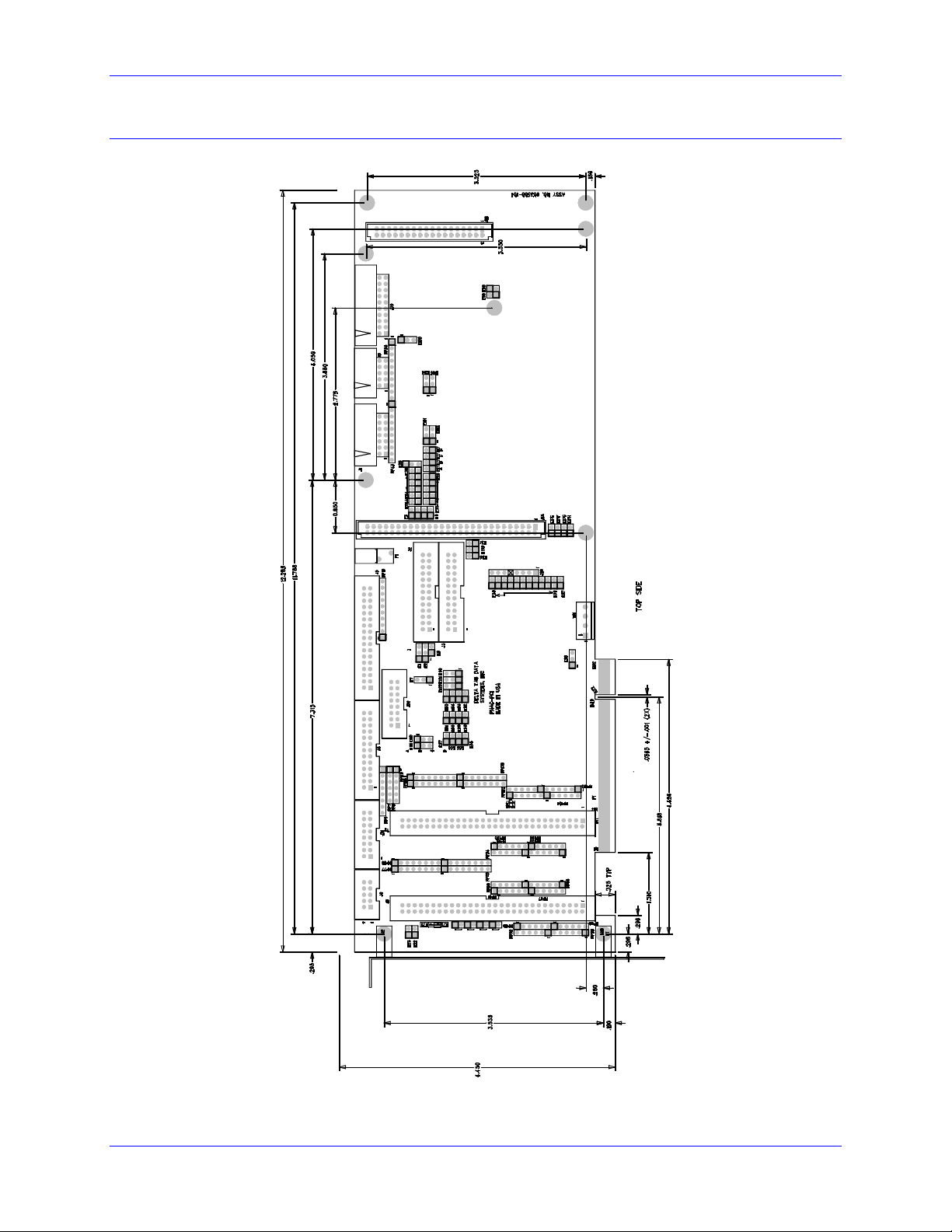
PMAC Board Layout Part Number 603588-100.......................................................................................................5
PMAC Connectors ....................................................................................................................................................7
JUMPER SUMMARY ................................................................................................................................................8
Power-Supply Configuration Jumpers ......................................................................................................................8
Clock Configuration Jumpers....................................................................................................................................9
Encoder Configuration Jumpers................................................................................................................................9
Board Reset/Save Jumpers ........................................................................................................................................9
Communication Jumpers.........................................................................................................................................10
I/O Configuration Jumpers......................................................................................................................................10
Reserved Configuration Jumpers ............................................................................................................................11
Piggyback CPU (FLEX) Board Jumper Configuration...........................................................................................11
Watchdog Timer Jumper.....................................................................................................................................11
Dual-Ported RAM Source Jumper......................................................................................................................11
Power-Up State Jumpers ....................................................................................................................................12
Firmware Load Jumper ......................................................................................................................................12
Flash Memory Bank Select Jumpers...................................................................................................................12
Installation...............................................................................................................................................................12
E-POINT DESCRIPTIONS......................................................................................................................................13
CPU Board E-Point Descriptions............................................................................................................................13
E1: Watchdog Disable Jumper ...........................................................................................................................13
E2: DPRAM Location Configure........................................................................................................................13
E4 – E6: Power-Up/Reset Load Source ..................................................................................................................13
E7: Firmware Reload Enable ..................................................................................................................................13
Main Board E-Point Jumper Descriptions...............................................................................................................14
Table of Contents i
Page 6

PMAC-PCI Hardware Reference
E0: Machine Output............................................................................................................................................14
E1 - E2: Machine Output Supply Voltage Configure..........................................................................................14
E3 - E6: Servo Clock Frequency Control..........................................................................................................15
E7: Machine Input Source/Sink Control............................................................................................................15
E17A-D: Amplifier Enable/Direction Polarity Control.....................................................................................16
E17E-H: Amplifier Enable/Direction Polarity Control......................................................................................16
E22 - E23: Control Panel Handwheel Enable...................................................................................................17
E28: Following Error/Watchdog Timer Signal Control.....................................................................................17
E29 - E33: Phase Clock Frequency Control......................................................................................................17
E34 - E38: Encoder Sampling Clock Frequency Control..................................................................................18
E40 - E43: Software Address Control................................................................................................................18
E44 - E47: Serial Port Baud Rate.......................................................................................................................19
E48: CPU Clock Frequency Control (Option CPU Section).............................................................................19
E49: Serial Communications Parity Control.....................................................................................................20
E50: Flash Save Enable/Disable .......................................................................................................................20
E51: Normal /Re-initializing Power-Up ............................................................................................................20
E54 - E65: Host Interrupt Signal Select ............................................................................................................20
E72 - E73: Panel Analog time Base Signal Enable...........................................................................................21
E74 - E75: Clock Output Control for Ext. Interpolation ...................................................................................22
E85: Host-Supplied Analog Power Source Enable............................................................................................22
E87 - E88: Host-Supplied Analog Power Source Enable..................................................................................22
E89: Amplifier-Supplied Switch Pull-Up Enable...............................................................................................22
E90: Host-Supplied Switch Pull-Up Enable ......................................................................................................23
E98: DAC/ADC Clock Frequency Control........................................................................................................23
E100: Output Flag Supply Select.......................................................................................................................23
E101 - E102: Motors 1-4 Amplifier Enable Output Configure..........................................................................24
E109: Reserved for Future Use .........................................................................................................................24
E110: Serial Port Configure..............................................................................................................................24
E111: Clock Lines Output Enable .....................................................................................................................25
E114 - E115: Motors 5-8 Amplifier Enable Output Configure...........................................................................25
E121 - E122: XIN Feature Selection .................................................................................................................26
MACHINE CONNECTIONS...................................................................................................................................27
Mounting .................................................................................................................................................................27
Power Supplies........................................................................................................................................................27
Digital Power Supply..........................................................................................................................................27
Analog Power Supply..........................................................................................................................................27
Flags Power Supply (optional) ...........................................................................................................................28
Overtravel Limits and Home Switches....................................................................................................................28
Resistor Pack Configuration: Flag and Digital Inputs Voltage Selection ..........................................................28
Types of Overtravel Limits..................................................................................................................................28
Home Switches....................................................................................................................................................29
Motor Signals Connections (JMACH Connectors).................................................................................................29
Resistor Pack Configuration: Termination Resistors .........................................................................................29
Resistor Pack Configuration: Differential or Single-Ended Encoder Selection................................................29
Incremental Encoder Connection .......................................................................................................................30
DAC Output Signals............................................................................................................................................30
Amplifier Enable Signal (AENAx/DIRn).............................................................................................................31
Amplifier Fault Signal (FAULTn).......................................................................................................................32
General-Purpose Digital Inputs and Outputs (JOPTO Port)....................................................................................32
Control-Panel Port I/O (JPAN Port)........................................................................................................................33
Command Inputs.................................................................................................................................................33
Selector Inputs ....................................................................................................................................................33
Alternate Use ......................................................................................................................................................33
Reset Input ..........................................................................................................................................................34
Handwheel Inputs ...............................................................................................................................................34
ii Table of Contents
Page 7

PMAC-PCI Hardware Reference
Optional Voltage to Frequency Converter..........................................................................................................34
Thumbwheel Multiplexer Port (JTHW Port)...........................................................................................................35
Optional Analog Inputs (JANA Port)......................................................................................................................35
Compare Equal Outputs Port (JEQU Port)..............................................................................................................36
Serial Port (JRS422 Port) ........................................................................................................................................36
Machine Connections Example...............................................................................................................................37
MATING CONNECTORS .......................................................................................................................................39
Base Board Connectors ...........................................................................................................................................39
J1 (JDISP)/Display.............................................................................................................................................39
J2 (JPAN)/Control Panel....................................................................................................................................39
J3 (JTHW)/Multiplexer Port...............................................................................................................................39
J4 (JRS422)/RS232 or 422/Serial Communications ...........................................................................................39
J5 (JOPT)/OPTO I/O..........................................................................................................................................39
J6 (JXIO)/Expansion Board................................................................................................................................39
J7 (JMACH2)/2nd Machine Connector (Option 1 Required).............................................................................39
J8 (JMACH1)/1st Machine Connector ...............................................................................................................39
JS1/A-D Inputs 1-4..............................................................................................................................................40
JS2/A-D Inputs 5-8 (Option 1 Required) ............................................................................................................40
JEQU/Position Compare ....................................................................................................................................40
JANA/Analog Inputs Option ...............................................................................................................................40
CPU Board Connectors ...........................................................................................................................................40
J2 (JEXP)/Expansion..........................................................................................................................................40
J4 (JDPRAM)/Dual-Ported RAM .......................................................................................................................40
BASE BOARD CONNECTOR PINOUTS..............................................................................................................41
J1: Display Port Connector......................................................................................................................................41
J1 JDISP (14-Pin Connector).............................................................................................................................41
J2: Control Panel Port Connector............................................................................................................................42
J2 JPAN (26-Pin Connector)..............................................................................................................................42
J3: Multiplexer Port Connector ...............................................................................................................................43
J3 JTHW (26-Pin Connector) .............................................................................................................................43
J4: Serial Port Connector.........................................................................................................................................44
J4 JRS422 (26-Pin Connector) ...........................................................................................................................44
J5: I/O Port Connector.............................................................................................................................................45
J5 JOPT (34-Pin Connector)..............................................................................................................................45
J6: Auxiliary I/O Port Connector ............................................................................................................................46
J6 JXIO (10-Pin Connector)...............................................................................................................................46
J7: Machine Port 2 Connector.................................................................................................................................47
J7 JMACH2 (60-Pin Header) ............................................................................................................................47
Continued............................................................................................................................................................48
J8: Machine Port 1 Connector.................................................................................................................................49
J8 JMACH1 (60-Pin Header) ............................................................................................................................49
J9 (JEQU): Position-Compare Connector ...............................................................................................................51
J9 JEQU (10-Pin Connector) .............................................................................................................................51
J30 (JANA) Analog Input Port Connector (Optional).............................................................................................51
J31 (JUSB) Universal Serial Bus Port (Optional) ...................................................................................................52
JS1: A/D Port 1 Connector......................................................................................................................................52
JS1 (16-Pin Header) ...........................................................................................................................................52
JS2: A/D Port 2 Connector......................................................................................................................................53
JS2 (16-Pin Header) ...........................................................................................................................................53
TB1 (JPWR) ........................................................................................................................................................53
SOFTWARE SETUP ................................................................................................................................................55
Communications......................................................................................................................................................55
PMAC I-Variables...................................................................................................................................................55
Operation of the Non-Turbo CPU...........................................................................................................................55
Table of Contents iii
Page 8

PMAC-PCI Hardware Reference
Configuring PMAC with Option-5C for 80 MHz Operation ..................................................................................58
Option 16 Supplemental Memory ...........................................................................................................................59
SCHEMATICS ..........................................................................................................................................................61
iv Table of Contents
Page 9

PMAC-PCI Hardware Reference
Table of Contents v
Page 10

Page 11

PMAC-PCI Hardware Reference
INTRODUCTION
The PMAC PCI is a member of the PMAC family of boards optimized for interface to traditional servo
drives with single analog inputs representing velocity or torque commands. Its software is capable of 8
axes of control. It can have up either eight or four channels of on-board axis interface circuitry.
The PMAC PCI is a full-sized PCI-bus expansion card, with a small piggyback board containing the CPU
board. While the PMAC PCI is capable of PCI bus communications, with or without the optional dualported RAM, it does not need to be inserted into an PCI expansion slot. Communications can be done
through an RS-232 or RS-422 serial port; standalone operation is possible.
Board Configuration
Base Version
The base version of the PMAC PCI provides a 1-1/2-slot board with:
• 40 MHz DSP56002 CPU
• 128k x 24 0-wait-state flash-backed SRAM
• 512k x 8 flash memory for firmware and user backup
• 2k x 8 EEPROM memory for setup variable backup
• Latest released firmware version
• RS-422 serial interface, PCI (PC) bus interface
• Four channels axis interface circuitry, each including:
• 16-bit +/-10V analog output
• 3-channel differential/single-ended encoder input
• Four input flags, two output flags
• Interface to external 16-bit serial ADC
• Display, control panel, muxed I/O, direct I/O interface ports
• Buffered expansion port
• Clock crystal with +/-100 ppm accuracy
• PID/notch/feedforward servo algorithms
• 1-year warranty from date of shipment
• One manuals CD per set of 1 to 4 PMACs in shipment
(Cables, mounting plates, mating connectors not included)
Option 1: Additional Four Channels Axis Interface Circuitry
• Option 1 provides an additional four channels of on-board axis interface circuitry, identical to the
standard first four channels.
Option 2: Dual-Ported RAM
Dual-ported RAM provides a high-speed communications path for bus communications with the host
computer through a bank of shared memory. DPRAM is advised if more than 100 data items per second
are to be passed between the controller and the host computer in either direction.
• Option 2 provides an 8k x 16 bank of dual-ported RAM on-board.
• Option A provides a 20-cm (8") 50-pin 3-connector cable. This cable is necessary when using the
Option 2 board combined with any of the Acc-14D, 24P, 29P, or 36P boards.
Option 2B: High-Speed USB Communications Interface
Option-2B provides the high-speed USB communications interface, which is a faster method of
communication than the standard RS-232 communications port.
Introduction 1
Page 12

PMAC-PCI Hardware Reference
Option 5x: CPU Type
The base PMAC version without options has a 20 MHz CPU with flash memory RAM.
• Option 5A: 40 MHz CPU, zero-wait RAM, flash backup, no battery, (~100% speed increase)
• Option 5B: 60 MHz CPU, zero-wait RAM, flash backup, no battery, (~200% speed increase)
• Option 5C: 80 MHz CPU, zero-wait RAM, flash backup, no battery, (~375% speed increase)
Option 6: Extended Firmware Algorithm
• Option 6 provides an Extended (Pole-Placement) Servo Algorithm firmware instead of the regular
servo algorithm firmware. This is only required in difficult-to-control systems (resonances, backlash,
friction, disturbances, changing dynamics). This option requires a one-time purchase of the Acc-25
program, which is necessary for tuning the Option-6 firmware.
Option 7: Plate Mounting
• Option 7 provides a mounting plate connected to the PMAC with standoffs. It is used to install the
PMAC in standalone applications.
Option 8A: High-Accuracy Clock Crystal
The PMAC PCI has a clock crystal of nominal frequency 19.6608 MHz (~20 MHz). The standard
crystal’s accuracy specification is +/-100 ppm.
• Option 8A provides a nominal 19.6608 MHz crystal with a +/-15 ppm accuracy specification.
Option 10: Firmware Version Specification
Normally the PMAC PCI is provided with the newest released firmware version. A label on the memory
IC shows the firmware version loaded at the factory.
• Option 10 provides for a user-specified firmware version.
Option 12: Analog-to-Digital Converters
Option 12 permits the installation of 8 or 16 channels of on-board multiplexed analog-to-digital
converters. One or two of these converters are read every phase interrupt. The analog inputs are not
optically isolated, and each can have a 0 – 5V input range, or a +/-2.5V input range, individually
selectable.
• Option 12 provides an 8-channel 12-bit A/D converter. The key components on the board are U20
and connector J30.
• Option 12A provides an additional 8-channel 12-bit A/D converter. The key component on the board
is U22.
Option 15: V-to-F Converter for Analog Input
The JPAN control panel port on the PMAC PCI has an optional analog input called WIPER (because it is
often tied to a potentiometer’s wiper pin). PMAC PCI can digitize this signal by passing it through an
optional voltage-to-frequency converter, using E-point jumpers to feed this into the Encoder 4 circuitry
(no other use is then permitted), and executing frequency calculations using the “time base” feature of the
encoder conversion table.
• Option 15 provides a voltage-to-frequency converter that permits the use of the Wiper input on the
control panel port.
Option 16: Battery-Backed Parameter Memory
The contents of the standard memory are not retained through a power-down or reset unless they have
been saved to flash memory first. Option 16 provides supplemental battery-backed RAM for real-time
parameter storage that is ideal for holding machine state parameters in case of an unexpected powerdown.
Option 16A provides a 16k x 24 bank of battery-backed parameter RAM. This Option requires Option
4A, Option 5A, Option 5B or Option 5C.
2 Introduction
Page 13

PMAC-PCI Hardware Reference
PMAC Connectors and Indicators
J1 - Display Port (JDISP Port)
The JDISP connector allows connection of the Acc-12 or Acc-12A liquid crystal displays, or of the Acc12C vacuum fluorescent display. Both text and variable values may be shown on these displays using the
DISPLAY command, executing in either motion or PLC programs.
J2 - Control-Panel Port (JPAN Port)
The JPAN connector is a 26-pin connector with dedicated control inputs, dedicated indicator outputs, a
quadrature encoder input, and an analog input (requires PMAC Option 15). The control inputs are low
true with internal pull-up resistors. They have predefined functions unless the control-panel-disable Ivariable (I2) has been set to 1. If this is the case, they may be used as general-purpose inputs by assigning
M-variable to their corresponding memory-map locations (bits of Y address $FFC0).
J3 - Thumbwheel Multiplexer Port (JTHW Port)
The Thumbwheel Multiplexer Port, or Multiplexer Port, on the JTHW connector has eight input lines and
eight output lines. The output lines can be used to multiplex large numbers of inputs and outputs on the
port, and Delta Tau provides accessory boards and software structures (special M-variable definitions) to
capitalize on this feature. Up to 32 of the multiplexed I/O boards may be daisy-chained on the port, in
any combination.
J4 - Serial Port (JRS422 Port)
For serial communications, use a serial cable to connect your PC’s COM port to the PMAC’s serial port
connector. Delta Tau provides the Acc-3D cable for this purpose, which connects PMAC to a DB-25
connector. Standard DB-9-to-DB-25 or DB-25-to-DB-9 adapters may be needed for a particular setup.
J5 - General-Purpose Digital Inputs and Outputs (JOPTO Port)
PMAC’s JOPTO connector provides eight general-purpose digital inputs and eight general-purpose
digital outputs. Each input and each output has its own corresponding ground pin in the opposite row.
The 34-pin connector was designed for easy interface to OPTO-22 or equivalent optically isolated I/O
modules. Delta Tau’s Acc-21F is a six-foot cable for this purpose.
J6 – Expansion Port (JXIO Port)
This port is only used when connecting to optional PMAC accessory boards.
J7 / J8 - Machine Connectors (JMACH2 / JMACH1 Ports)
The primary machine interface connector is JMACH1, labeled J8 on the PMAC PCI. It contains the pins
for four channels of machine I/O: analog outputs, incremental encoder inputs, and associated input and
output flags, plus power-supply connections. The next machine interface connector is JMACH2, labeled
J7 on the PMAC PCI. Essentially, it is identical to the JMACH1 connector for one to four more axes. It
is present only if the PMAC card has been fully populated to handle eight axes (Option 1), because it
interfaces the optional extra components.
J9 – Compare Equal Outputs Port (JEQU Port)
The compare-equals (EQU) outputs have a dedicated use of providing a signal edge when an encoder
position reaches a pre-loaded value. This is useful for scanning and measurement applications.
Instructions for use of these outputs are covered in detail in the PMAC’s User Manual.
J30 – Optional Analog to Digital Inputs (JANA Port)
This optional port is used to bring in the analog signals for the optional analog to digital inputs set. This
feature provides up to 16 analog inputs in the range of 0 to 5V unipolar or ±2.5V bipolar.
J31 – Optional Universal Serial Bus Port (JUSB Port)
This optional port allows communicating with PMAC through a standard USB connection.
Introduction 3
Page 14

PMAC-PCI Hardware Reference
JS1/JS2 – Expansion Ports (JS1/JS2 Ports)
These ports are used only when connecting to optional PMAC accessory boards.
TB1 – Power Supply Terminal Block (JPWR Connector)
This terminal block may be used as an alternative power supply connector if PMAC PCI is not installed
in a PCI-bus.
LED Indicators
PMACs with the Option CPU have three LED indicators: red, yellow, and green. The red and green
LEDs have the same meaning as with the standard CPU: when the green LED is lit, this indicates that
power is applied to the +5V input; when the red LED is lit, this indicates that the watchdog timer has
tripped and shut down the PMAC.
The yellow LED located beside the red and green LEDs, when lit, indicates that the phase-locked loop
that multiplies the CPU clock frequency from the crystal frequency on the Option CPU is operational and
stable. This indicator is for diagnostic purposes only; it may not be present on your board.
The PMAC PCI has an interlock circuit that drops out the ±15V supplies to the analog outputs through a
fail-safe relay if any supply on PMAC is lost. In this case, the green LED D15 will be off. The D19 LED
will be lit when 5V is applied to PMAC.
4 Introduction
Page 15

PMAC-PCI Hardware Reference
PMAC Board Layout Part Number 603588-100
Feature Location Feature Location
E0 A6 E57 B7
E1 A6 E58 B7
E2 A6 E59 B7
E3 A4 E60 B7
E4 A4 E61 B7
E5 A4 E62 B6
E6 A4 E63 B6
E7 A6 E64 B6
E17A A4 E65 B6
E17B A4 E72 B9
E17C A4 E73 B9
E17D A4 E74 B9
E17E C5 E75 B9
E17F C5 E85 C5
E17G C4 E87 C5
E17H C4 E88 B2
E22 A9 E89 B5
E23 A9 E90 B5
E28 C6 E98 A4
E29 A4 E100 A3
E30 A4 E101 A3
E31 A4 E102 A3
E32 A4 E109 B6
E33 A4 E110 A7
E34 A4 E111 A7
E34A A4 E114 A3
E35 A4 E115 A3
E36 A4 E121 B6
E37 A4 E122 B6
E38 A4 D15 C1
E40 B5 D19 B6
E41 B5 J1 A4
E42 B5 J2 A6
E43 B5 J3 B6
E44 B5 J4 A7
E45 B5 J5 A5
E46 C5 J6 A9
E47 C5 J7 A8
E48 C5 J8 A9
E49 C5 J9 A2
E50 C5 J30 A1
E51 B6 J31 A5
E54 B7 JS1 A8
E55 B7 JS2 A6
E56 B7 TB1 C6
Introduction 5
Page 16

PMAC-PCI Hardware Reference
1
2
E17D
E17C
E17B
E38 E17A
E37 E29
E36 E30
E35 E31
E34 E32
E34A E33
3
E3
E4
E5
E6
4
5
6
E57 E61 E65
E56 E60 E64
E55 E59 E63
E54 E58 E62
7
8
9
B A
C
6 Introduction
Page 17
PMAC-PCI Hardware Reference
PMAC Connectors
Introduction 7
Page 18
PMAC-PCI Hardware Reference
JUMPER SUMMARY
On the PMAC, you will see many jumpers (pairs of metal prongs), called E-points. Some have been
shorted together; others have been left open. These jumpers customize the hardware features of the board
for a given application and must be setup appropriately. The following is an overview of the several
PMAC jumpers grouped in appropriate categories. For a complete description of the jumper setup
configuration, refer to the PMAC PCI CPU Board E-Point Descriptions section in this manual.
Power-Supply Configuration Jumpers
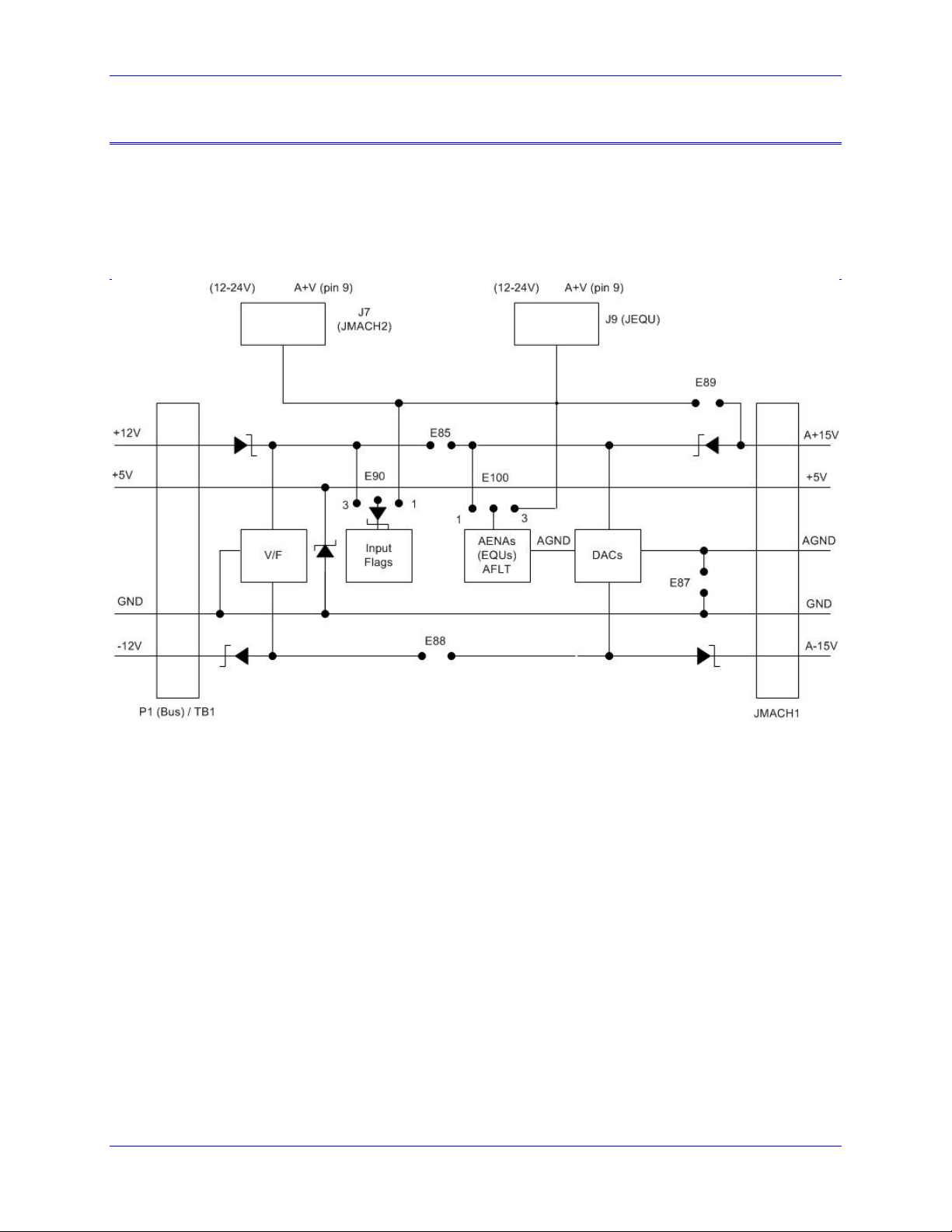
E85, E87, E88: Analog Circuit Isolation Control – These jumpers control whether the analog circuitry
on the PMAC PCI is isolated from the digital circuitry, or electrically tied to it. In the default
configuration, these jumpers are off, keeping the circuits isolated from each other (provided separate
isolated supplies are used).
E89-E90: Input Flag Supply Control – If E90 connects pins 1 and 2 and E89 is ON, the input flags
(+LIMn, -LIMn, and HMFLn) are supplied from the analog A+15V supply, which can be isolated from
the digital circuitry. If E90 connects pins 1 and 2 and E89 is OFF, the input flags are supplied from a
separate A+V supply brought in on pin 59 of the J7 JMACH2 connector. This supply can be in the +12V
to +24V range, and can be kept isolated from the digital circuitry. If E90 connects pins 2 and 3, the input
flags are supplied from the digital +12V supply, and isolation from the digital circuitry is defeated.
E100: AENA/EQU Supply Control – If E100 connects pins 1 and 2, the circuits related to the AENAn,
EQUn and FAULTn signals will be supplied from the analog A+15V supply, which can be isolated from
the digital circuitry. If E100 connects pins 2 and 3, the circuits will be supplied from a separate A+V
supply brought in on pin 9 of the J9 JEQU connector. This supply can be in the +12V to +24V range, and
can be kept isolated from the digital circuitry.
8 Jumper Summary
Page 19

PMAC-PCI Hardware Reference
Clock Configuration Jumpers
E3-E6: Servo Clock Frequency Control – The jumpers E3 – E6 determine the servo-clock frequency
by controlling how many times it is divided down from the phase-frequency. The default setting of E3
and E4 OFF, E5 and E6 ON divides the phase-clock frequency by 4, creating a 2.25 kHz servo-clock
frequency. This setting is seldom changed.
E29-E33: Phase Clock Frequency Control – Only one of the jumpers E29 – E33, which select the
phase-clock frequency, may be on in any configuration. The default setting of E31 ON, which selects a 9
kHz phase-clock frequency, is seldom changed.
E34-E38: Encoder Sample Clock – Only one of the jumpers E34 – E38, which select the encoder
sample clock frequency, may be on in any configuration. The frequency must be high enough to accept
the maximum true count rate (no more than one count in any clock period), but a lower frequency can
filter out longer noise spikes. The anti-noise digital delay filter can eliminate noise spikes up to one
sample-clock cycle wide.
E40-43: Servo and Phase Clock Direction Control – Jumpers E40-E43 control the software address of
the card, for serial addressing and for sharing the servo and phase clock over the serial connector. Card
@0 sends the clocks and cards @1-@F receive the clocks. If any of these jumpers is removed, PMAC
PCI will expect to receive external servo and phase clock signals on the J4 serial port – if these signals are
not provide in this configuration, the watchdog timer will immediately trip.
E48: Option CPU Clock Frequency Control – When PMAC is ordered with Option 5B, E48 setup the
CPU clock frequency to either 40 MHz or 60 MHz. If PMAC is ordered with Option 5C additional
software, setup is necessary for 80 MHz CPU clock frequency operation.
E98: DAC/ADC Clock Frequency Control – Leave E98 in its default setting of 1-2, which creates a
2.45 MHz DCLK signal, unless you are connecting an Acc-28 A/D-converter board. In this case, move
the jumper to connect pins 2 and 3, which creates a 1.22 MHz DCLK signal.
Encoder Configuration Jumpers
Encoder Complementary Line Control – The selection of the type of encoder used, either single ended
or differential is made through the resistor packs configuration and not through a jumper configuration.
E22-E23: Control-Panel Handwheel Enable – Putting these jumpers ON ties the handwheel-encoder
inputs on the JPAN control-panel port to the Channel 2 encoder circuitry. If the handwheel inputs are
connected to Channel 2, no encoder should be connected to Channel 2 through the JMACH1 connector.
E72-E73: Control Panel Analog Input Enable – Putting these jumpers ON ties the output of the Option
10 voltage-to-frequency converter that can process the “WIPER” analog input on the JPAN control panel
port to the Channel 4 encoder circuitry. If the frequency signal is connected to Channel 4, no encoder
should be connected to Channel 4 through the JMACH1 connector.
E74-E75: Encoder Sample Clock Output – Putting these jumpers ON ties the encoder sample-clock
signal to the CHC4 and CHC4/ lines on the JMACH1 port. This permits the clock signal to be used to
synchronize external encoder-processing devices like the Acc-8D Option 8 interpolator board. With these
jumpers ON, no encoder input signal should be connected to these pins.
Board Reset/Save Jumpers
E50: Flash-Save Enable/Disable Control – If E50 is ON (default), the active software configuration of
the PMAC can be stored to non-volatile flash memory with the SAVE command. If the jumper on E50 is
removed, this SAVE function is disabled, and the contents of the flash memory cannot be changed.
E51: Re-Initialization on Reset Control – If E51 is OFF (default), PMAC executes a normal reset,
loading active memory from the last saved configuration in non-volatile flash memory. If E51 is ON,
PMAC re-initializes on reset, loading active memory with the factory default values.
Jumper Summary 9
Page 20

PMAC-PCI Hardware Reference
Communication Jumpers
PCI Bus Base Address Control – The selection of the base address of the card in the I/O space of the
host PC’s expansion bus is assigned automatically by the operating system and it is not selected through a
jumper configuration.
E44-E47: Serial Baud Rate Selection –The configuration of these jumpers and the particular CPU
Option ordered will determine the baud rate at which PMAC will communicate through its J4 serial port.
For example, when PMAC is ordered with no CPU Options and only the jumpers E45 and E46 are
installed, the baud rate will be set at 9600 baud.
E49: Serial Communications Parity Control – Jump pin 1 to 2 for NO serial parity; remove jumper for
ODD serial parity.
E54-E65: Interrupt Source Control – These jumpers control which signals are tied to interrupt lines
IR5, IR6 and IR7 on PMAC’s programmable interrupt controller (PIC), as shown in the interrupt
diagram. Only one signal may be tied into each of these lines.
E110: Serial Port Configure – Jump pin 1 to 2 for use of the J4 connector as RS-232. Jump pin 2 to 3
for use of the J4 connector as RS-422.
E111: Clock Lines Output Enable – Jump pin 1 to 2 to enable the Phase, Servo and INIT lines on the
J4 connector. Jump pin 2 to 3 to disable the Phase, Servo and INIT lines on the J4 connector. E111 on
positions 1 to 2 is necessary for daisy-chained PMACs sharing the clock lines for synchronization.
I/O Configuration Jumpers
WARNING:
A wrong setting of these jumpers will damage the associated output IC.
E1-E2: Machine Output Supply Configure – With the default sinking output driver IC (ULN2803A or
equivalent) in U13 for the J5 JOPTO port outputs, these jumpers must connect pins 1 and 2 to supply the
IC correctly. If this IC is replaced with a sourcing output driver IC (UDN2981A or equivalent), these
jumpers must be changed to connect pins 2 and 3 to supply the new IC correctly.
E7: Machine Input Source/Sink Control – With this jumper connecting pins 1 and 2 (default) the
machine input lines on the J5 JOPTO port are pulled up to +5V or the externally provided supply voltage
for the port. This configuration is suitable for sinking drivers. If the jumper is changes to connect pins 2
and 3, these lines are pulled down to GND – this configuration is suitable for sourcing drivers.
E17A - E17D: Motors 1-4 Amplifier-Enable Polarity Control – Jumpers E17A through E17D control
the polarity of the amplifier enable signal for the corresponding motor 1 to 4. When the jumper is ON
(default), the amplifier-enable line for the corresponding motor is low true so the enable state is lowvoltage output and sinking current, and the disable state is not conducting current. With the default
ULN2803A sinking driver used by the PMAC PCI on U37, this is the fail-safe option, allowing the circuit
to fail in the disable state. With this jumper OFF, the amplifier-enable line is high true so the enable state
is not conducting current, and the disable state is low-voltage output and sinking current. This setting is
not generally recommended.
E17E - E17H: Motors 5-8 Amplifier-Enable Polarity Control – Jumpers E17A through E17D control
the polarity of the amplifier enable signal for the corresponding motor 5 to 8. When the jumper is ON
(default), the amplifier-enable line for the corresponding motor is low true so the enable state is lowvoltage output and sinking current, and the disable state is not conducting current. With the default
ULN2803A sinking driver used by the PMAC PCI on U53, this is the fail-safe option, allowing the circuit
to fail in the disable state. With this jumper OFF, the amplifier-enable line is high true so the enable state
is not conducting current, and the disable state is low-voltage output and sinking current. Generally, this
setting is not recommended.
10 Jumper Summary
Page 21

PMAC-PCI Hardware Reference
E28: Following-Error/Watchdog-Timer Signal Control – With this jumper connecting pins 2 and 3
(default), the FEFCO/ output on pin 57 of the J8 JMACH1 servo connector outputs the watchdog timer
signal. With this jumper connecting pins 1 and 2, this pin outputs the warning following error status line
for the selected coordinate system.
WARNING:
A wrong setting of these jumpers will damage the associated output IC.
E101-E102: Motors 1-4 AENA/EQU voltage configure – The U37 driver IC controls the AENA and
EQU signals of motors 1-4. With the default sinking output driver IC (ULN2803A or equivalent) in U37,
these jumpers must connect pins 1 and 2 to supply the IC correctly. If this IC is replaced with a sourcing
output driver IC (UDN2981A or equivalent), these jumpers must be changed to connect pins 2 and 3 to
supply the new IC correctly.
WARNING:
A wrong setting of these jumpers will damage the associated output IC.
E114-E115: Motors 5-8 AENA/EQU voltage configure – The U53 driver IC controls the AENA and
EQU signals of motors 5-8. With the default sinking output driver IC (ULN2803A or equivalent) in U53,
these jumpers must connect pins 1 and 2 to supply the IC correctly. If this IC is replaced with a sourcing
output driver IC (UDN2981A or equivalent), these jumpers must be changed to connect pins 2 and 3 to
supply the new IC correctly.
E121: XIN6 Motor Selection – Jump 1-2 to bring the QuadLoss signal for Encoder 6 into register XIN6
at Y:$E801 bit 6. Jump 2-3 to bring the QuadLoss signal for Encoder 7 into register XIN6 at Y:$E801 bit
6.
E122: XIN7 Feature Selection – Jump 1-2 to bring the QuadLoss signal for Encoder 8 into register
XIN7 at Y:$E801 bit 7. Jump 2-3 to bring the PowerGood signal into register XIN7 at Y:$E801 bit 7.
Reserved Configuration Jumpers
E109: Reserved for future use
Piggyback CPU (FLEX) Board Jumper Configuration
Watchdog Timer Jumper
Jumper E1 on the Non-Turbo CPU board must be OFF for the watchdog timer to operate. This is a very
important safety feature, so it is vital that this jumper be OFF in normal operation. E1 should only be put
ON to debug problems with the watchdog timer circuit.
Dual-Ported RAM Source Jumper
Jumper E2 must connect pins 1 and 2 to access dual-ported RAM (non-Turbo addresses $Dxxx, Turbo
addresses $06xxxx) from the base board. If it is desired to use the Option 2 DPRAM on the base board,
jumper E2 must be in this setting. All Delta Tau base boards except the PMAC(1)-PC board have the
option for installing DPRAM on the base board.
Jumper E2 must connect pins 2 and 3 to access dual-ported RAM (non-Turbo addresses $Dxxx, Turbo
addresses $06xxxx) through the JEXP expansion port. If it is desired to use DPRAM on an external
accessory board, jumper E2 must be in this setting. The PMAC(1)-PC base board (part # 602191-10x)
does not have the option for installing on-board DPRAM; it requires the external Option 2 DPRAM board
(part #602240-10x) for this functionality. Use of this DPRAM board, interfacing through the JEXP port,
requires E2 to connect pins 2 and 3.
Jumper Summary 11
Page 22

PMAC-PCI Hardware Reference
Power-Up State Jumpers
Jumper E4 on the Non-Turbo CPU board must be OFF, jumper E5 must be ON, and jumper E6 must be
ON, in order for the CPU to copy the firmware from flash memory into active RAM on power-up/reset.
This is necessary for normal operation of the card. (Other settings are for factory use only.)
Firmware Load Jumper
If jumper E7 on the CPU board is ON during power-up/reset, the board comes up in “bootstrap mode”,
which permits the loading of new firmware into the flash-memory IC on the board. When the PMAC
Executive program tries to establish communications with a board in this mode, it will automatically
detect that the board is in bootstrap mode and ask you what file you want to download as the new
firmware.
Jumper E7 must be OFF during power-up/reset for the board to come up in normal “operational mode”.
Flash Memory Bank Select Jumpers
The flash-memory IC in location U10 on the Flex CPU board has the capacity for eight separate banks of
firmware, only one of which can be used at any given time. The eight combinations of settings for
jumpers E10A, E10B, and E10C select which bank of the flash memory is used. In the factory production
process, firmware is loaded only into Bank 0, which is selected by having all of these jumpers OFF.
Installation
The Flex CPU board installs on the base controller board using the P1 and P3 stack connectors on the
solder side of the CPU board. The CPU board can be further secured to the base board with a standoff
and screw through the central hole. When a complete PMAC or Turbo PMAC controller is purchased,
this assembly is done at the factory. In the case of retrofits or updates to existing controllers, this
assembly is easy to do in the field.
WARNING:
The Flex CPU board and PMAC controller boards contain static-sensitive
components. Make sure proper ESD protection is employed.
12 Jumper Summary
Page 23

PMAC-PCI Hardware Reference
E-POINT DESCRIPTIONS
CPU Board E-Point Descriptions
The following jumper descriptions are for the PMAC CPU part number 602705-107.
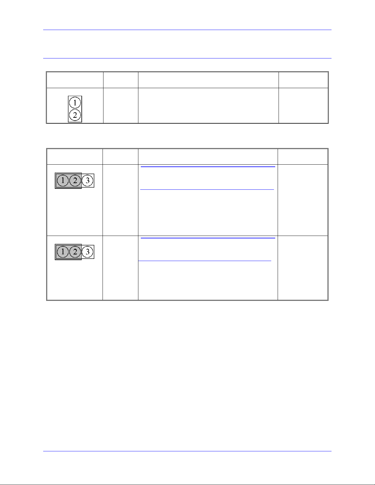
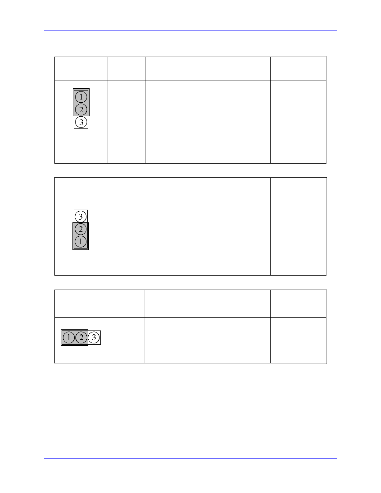
E1: Watchdog Disable Jumper
E Point and
Physical Layout
E1
Description Default
Jump pin 1 to 2 to disable Watchdog timer (for test purposes only).
Remove jumper to enable Watchdog timer.
No Jumper
E2: DPRAM Location Configure
E Point and
Physical Layout
E2
Note: Jumper E2 is present on –108 and newer boards only. Older versions could access DPRAM from either
source without a jumper configuration, but with less robust buffering.
Description Default
Jump pin 1 to 2 to access the dual-ported RAM on baseboard.
Jump pin 2 to 3 to access the dual-ported RAM through JEXP
expansion port.
Jumper connects
pins 1 and 2
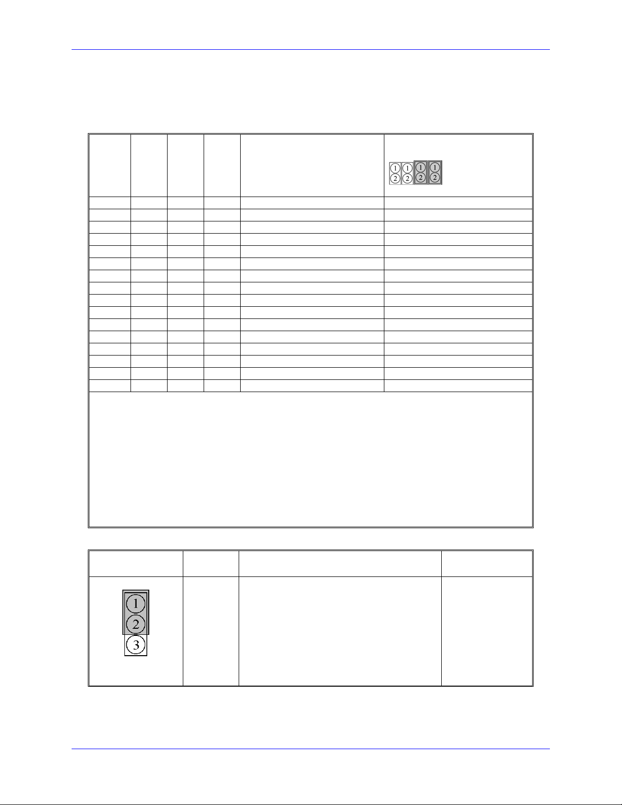
E4 – E6: Power-Up/Reset Load Source
E Point and
Physical Layout
E4
Remove jumper E4; jump E5 pin 1 to 2; jump E6
pin 1 to 2 to read flash IC on power-up/reset.
Description Default
No E4 jumper installed;
E5 and E6 jump pin 1 to 2.
E6
Note: Other combinations are for factory use only; the board will not operate in any other configuration
E7: Firmware Reload Enable
E Point and
Physical Layout
E7
Jump pin 1 to 2 to reload firmware through serial
or bus port.
Remove jumper for normal operation.
Description Default
No jumper installed
PMAC-PCI E-Point Jumper Descriptions 13
Page 24
PMAC-PCI Hardware Reference
Main Board E-Point Jumper Descriptions
E0: Machine Output
E Point and
Physical Layout
E0
E1 - E2: Machine Output Supply Voltage Configure
Location Description Default
A6
Jump pin 1 to 2
To provide use of 5V outputs
No jumper
E Point and
Physical Layout
E1
E2
Location Description Default
A6
The jumper setting must match the type of driver IC,
A6
or damage to the IC will result.
Jump pin 1 to 2 to apply +V (+5V to 24V) to pin 10
of U13 (should be ULN2803A for sink output
configuration) JOPTO machine outputs M01-M08.
Jump pin 2 to 3 to apply GND to pin 10 of U13
(should be UDN2981A for source output
configuration).
The jumper setting must match the type of driver IC,
or damage to the IC will result.
Jump pin 1 to 2 to apply GND to pin 10 of U13
(should be ULN2803A for sink output configuration).
Jump pin 2 to 3 to apply +V (+5V to 24V) to pin 10
of U13 (should be UDN2981A for source output
configuration).
CAUTION
CAUTION
1-2 Jumper
installed
1-2 Jumper
installed
14 PMAC-PCI E-Point Jumper Descriptions
Page 25
PMAC-PCI Hardware Reference
E3 - E6: Servo Clock Frequency Control
The servo clock (which determines how often the servo loop is closed) is derived from the phase clock
(see E98, E29 - E33) through a divide-by-N counter. Jumpers E3 through E6 control this dividing
function.
E3 E4 E5 E6 Servo Clock = Phase Clock
Divided by N
Default and Physical Layout
E3 E4 E5 E6
Location A4 A4 A4 A4
ON ON ON ON N = divided by 1
OFF ON ON ON N = divided by 2
ON OFF ON ON N = divided by 3
OFF OFF ON ON N = divided by 4 Only E5 and E6 on
ON OFF ON ON N = divided by 5
OFF ON OFF ON N = divided by 6
ON OFF OFF ON N = divided by 7
OFF OFF OFF ON N = divided by 8
ON ON ON OFF N = divided by 9
OFF ON ON OFF N = divided by 10
ON OFF ON OFF N = divided by 11
OFF OFF ON OFF N = divided by 12
ON ON OFF OFF N = divided by 13
OFF ON OFF OFF N = divided by 14
ON OFF OFF OFF N = divided by 15
OFF OFF OFF OFF N = divided by 16
Note: The setting of I-variable I10 should be adjusted to match the servo interrupt cycle time set by E98,
E3 -- E6, E29 -- E33, and the crystal clock frequency. I10 holds the length of a servo interrupt cycle,
scaled so that 8,388,608 equals one millisecond. Since I10 has a maximum value of 8,388,607, the servo
interrupt cycle time should always be less than a millisecond (unless you want to make your basic unit of
time on PMAC something other than a millisecond). If you wish a servo sample time greater than one
millisecond, the sampling may be slowed in software with variable Ix60.
Frequency can be checked on J4 pins 21 & 22. It can also be checked from software by typing RX:0 in
the PMAC terminal at 10-second intervals and dividing the difference of successive responses by 10000.
The resulting number is the approximate Servo Clock frequency kHz.
Note: If E40-E43 are not all on, the phase clock is received from an external source through the J4 serialport connector, and the settings of E3 – E6 are not relevant.
E7: Machine Input Source/Sink Control
E Point and
Physical Layout
E7
PMAC-PCI E-Point Jumper Descriptions 15
Location Description Default
A6 Jump pin 1 to 2 to apply +5V to input
reference resistor sip pack; this will bias MI1
to MI8 inputs to +5V for OFF state; input
must then be grounded for on state.
Jump pin 2 to 3 to apply GND to input
reference resistor sip pack; this will bias MI1
to MI8 inputs to GND for OFF state; input
must then be pulled up for on state (+5V to
+24V).
1-2 Jumper
installed
Page 26

PMAC-PCI Hardware Reference
E17A-D: Amplifier Enable/Direction Polarity Control
E Point and
Physical Layout
E17A
E17B
E17C
E17D
Note: Low-true enable is the fail-safe option because of the sinking (open-collector) ULN2803A output
driver IC.
Location Description Default
A4 Jump 1-2 for high-true AENA1.
Remove jumper for low-true AENA1.
A4 Jump 1-2 for high-true AENA2.
Remove jumper for low-true AENA2.
A4 Jump 1-2 for high-true AENA3.
Remove jumper for low-true AENA3.
A4 Jump 1-2 for high-true AENA4.
Remove jumper for low-true AENA4.
No jumper
installed
No jumper
installed
No jumper
installed
No jumper
installed
E17E-H: Amplifier Enable/Direction Polarity Control
E Point and
Physical Layout
E17E
E17F
E17G
E17H
Note: Low-true enable is the fail-safe option because of the sinking (open-collector) ULN2803A output
driver IC.
Location Description Default
C5 Jump 1-2 for high-true AENA5.
Remove jumper for low-true AENA1.
C5 Jump 1-2 for high-true AENA6.
Remove jumper for low-true AENA2.
C4 Jump 1-2 for high-true AENA7.
Remove jumper for low-true AENA3.
C4 Jump 1-2 for high-true AENA8.
Remove jumper for low-true AENA4.
No jumper
installed
No jumper
installed
No jumper
installed
No jumper
installed
16 PMAC-PCI E-Point Jumper Descriptions
Page 27

PMAC-PCI Hardware Reference
E22 - E23: Control Panel Handwheel Enable
E Point and
Physical Layout
E22
E23
Note: With these jumpers ON, no encoder should be wired into ENC2 on JMACH1. Jumper E26 must
connect pins 1-2, because these are single-ended inputs. This function is unrelated to the encoder brought
in through Acc-39 on J2.
Location Description Default
A9 Jump pin 1 to 2 to obtain handwheel encoder
signal from front panel at J2-16 for CHB2
(ENC2-B).
A9 Jump pin 1 to 2 to obtain handwheel encoder
signal from front panel at J2-22 for CHA2
(ENC2-A).
No jumper
No jumper
E28: Following Error/Watchdog Timer Signal Control
E Point and
Physical
Layout
E28
Location Description Default
C6 Jump pin 1 to 2 to allow warning following
error (Ix12) for the selected coordinate system
to control FEFCO/ on J8-57.
Jump pin 2 to 3 to cause Watchdog timer
output to control FEFCO/.
Low TRUE output in either case.
2-3 Jumper
installed
E29 - E33: Phase Clock Frequency Control
Jumpers E29 through E33 control the speed of the phase clock, and, indirectly, the servo clock, which is
divided down from the phase clock (see E3 - E6). No more than 1 of these 5 jumpers may be on at a time.
E29 E30 E31 E32 E33
ON OFF OFF OFF OFF 2.26 kHz 1.13 kHz
OFF ON OFF OFF OFF 4.52 kHz 2.26 kHz
OFF OFF ON OFF OFF 9.04 kHz 4.52 kHz
OFF OFF OFF ON OFF 18.07 kHz 9.04 kHz
OFF OFF OFF OFF ON 36.14 kHz 18.07 kHz
Note: If E40-E43 are not all ON, the phase clock is received from an external source through the J4 serialport connector, and the settings of E29 – E33 are not relevant.
Phase Clock Frequency
E98 Connects
Pins 1 and 2
E98 Connects
Pins 2 And 3
Default and
Physical
Layout
E29
E30
E31
E32
E33
Location
A4
A4
A4
A4
A4
PMAC-PCI E-Point Jumper Descriptions 17
Page 28

PMAC-PCI Hardware Reference
E34 - E38: Encoder Sampling Clock Frequency Control
Jumpers E34 - E38 control the encoder-sampling clock (SCLK) used by the gate array ICs. No more than
one of these six jumpers may be on at a time.
E34A E34 E35 E36 E37 E38 SCLK Clock
Frequency
ON OFF OFF OFF OFF OFF 19.6608 MHz
OFF ON OFF ON OFF OFF 9.8304 MHz E34 ON
OFF OFF ON OFF OFF OFF 4.9152 MHz
OFF OFF OFF ON OFF OFF 2.4576 MHz
OFF OFF OFF OFF ON OFF 1.2288 MHz
OFF OFF OFF OFF OFF ON External clock 1 to 30 MHz
maximum input on CHC4
and CHC4/
Default and
Physical Layout
E34A E34 E35 E36 E37 E38
A4 A4 A4 A4 A4 A4
E40 - E43: Software Address Control
Jumpers E40-E43 control the software address of the card, for serial addressing and for sharing the servo
and phase clock over the serial connector. Card @0 sends the clocks and cards @1-@F receive the clocks.
Card Address Control
E Points
E40 E41 E42 E43 Card Address
ON ON ON ON @0 @0
OFF ON ON ON @1
ON OFF ON ON @2
OFF OFF ON ON @3
ON ON OFF ON @4
OFF ON OFF ON @5
ON OFF OFF ON @6
OFF OFF OFF ON @7
ON ON ON OFF @8
OFF ON ON OFF @9
ON OFF ON OFF @A
OFF OFF ON OFF @B
ON ON OFF OFF @C
OFF ON OFF OFF @D
ON OFF OFF OFF @E
OFF OFF OFF OFF @F
Note: The card must either be set up as @0, or receiving clock signals over the serial port from another
card that is set up as @0, or the watchdog timer will trip (red light ON) and the card will shut down.
Default and Physical Layout
E40 E41 E42 E43
Location B5 B5 B5 B5
18 PMAC-PCI E-Point Jumper Descriptions
Page 29

PMAC-PCI Hardware Reference
E44 - E47: Serial Port Baud Rate
Jumpers E44 - E47 control what baud rate to use for serial communications. Any character received over
the bus causes PMAC to use the bus for its standard communications. The serial port is disabled if E44E47 are all on. The baud rate setting of an 80 MHz CPU section ordered with Opt 5C is performed by
software; refer to the dedicated section on the Software Configuration chapter of this manual.
Baud Rate Control E Points Baud Rate
E44 E45 E46 E47 Option
4A
ON ON ON ON Disabled Disabled Disabled
OFF ON ON ON 300 600 900
ON OFF ON ON 400* 800* 1200
OFF OFF ON ON 600 1200 1800
ON ON OFF ON 800* 1600* 2400
OFF ON OFF ON 1200 2400 3600
ON OFF OFF ON 1600* 3200* 4800
OFF OFF OFF ON 2400 4800 7200
ON ON ON OFF 3200* 6400* 9600 Options 5, 5B
OFF ON ON OFF 4800 9600 14400 Std., Option 5A
ON OFF ON OFF 6400* 12800* 19200
OFF OFF ON OFF 9600 19200 28800 Option 4A
ON ON OFF OFF 12800* 25600* 38400
OFF ON OFF OFF 19200 38400 57600
ON OFF OFF OFF 25600* 51200* 76800
OFF OFF OFF OFF 38400 76800 115200
Note: These jumpers are only used to set the baud rate at power-on/reset. Currently, Flex CPU’s
communication baud rate is determined at power-up/reset by variable I54.
* Non-standard baud rates.
Standard,
Option
5A
Option 5,
Option
5B
Default and
Physical Layout
E44 E45 E46 E47
Loc. B5 B5 C5 C5
Picture is for a PMAC
with a Standard or
Option 5A CPU
E48: CPU Clock Frequency Control (Option CPU Section)
E48 controls the CPU clock frequency only on PMAC with an option CPU section using flash memory
backup (no battery). This CPU section is used on PMACs ordered with Opt 4A, 5A, or 5B. The 80 MHz
setting of a CPU section ordered with Opt 5C is performed by software; refer to the dedicated section on
the Software Configuration chapter of this manual.
E Point and
Physical Layout
E48
Note: It may be possible to operate a board with 40 MHz components (Option 5A) at 60 MHz under
some conditions by changing the setting of jumper E48. However, this operates the components outside
of their specified operating range, and proper execution of PMAC under these conditions is not
guaranteed. PMAC software failure is possible, even probable, under these conditions, and this can lead
to very dangerous machine failure. Operation in this mode is done completely at the user’s own risk.
Delta Tau can accept no responsibility for the operation of PMAC or the machine under these conditions.
Location Description Default
C5 Jump pins 1 and 2 to multiply crystal frequency
by 3 inside CPU for 60 MHz operation.
Remove jumper to multiply crystal frequency
by 2 inside CPU for 40 MHz operation.
Jumper installed
(Option 5, 5B)
Jumper not
installed (Standard,
Option 4A, 5A)
PMAC-PCI E-Point Jumper Descriptions 19
Page 30

PMAC-PCI Hardware Reference
E49: Serial Communications Parity Control
E Point and
Physical Layout
E49
Location Description Default
C5 Jump pin 1 to 2 for NO serial parity. Remove
jumper for ODD serial parity.
E50: Flash Save Enable/Disable
E Point and
Physical Layout
E50
Location Description Default
C5 Jump pin 1 to 2 to enable save to flash
memory.
Remove jumper to disable save to flash
memory.
E51: Normal /Re-initializing Power-Up
E Point and
Physical Layout
E51
Location Description Default
B6 Jump pin 1 to 2 to re-initialize ON power-
up/reset;
Remove jumper for Normal power-up/reset.
E54 - E65: Host Interrupt Signal Select
Jumper installed
Jumper Installed
No jumper
installed
E Point and
Physical Layout
E54
E55
E56
E57
Location Description Default
B7 Jump pin 1 to 2 to allow EQU8 to interrupt
host-PC at PMAC interrupt level IR7.
B7 Jump pin 1 to 2 to allow EQU4 to interrupt
host-PC at PMAC interrupt level IR7.
B7 Jump pin 1 to 2 to allow EQU7 to interrupt
host-PC at PMAC interrupt level IR7.
B7 Jump pin 1 to 2 to allow EQU3 to interrupt
host-PC at PMAC interrupt level IR7.
No jumper
installed
No jumper
installed
No jumper
installed
No jumper
installed
20 PMAC-PCI E-Point Jumper Descriptions
Page 31

PMAC-PCI Hardware Reference
E54 - E65: Host Interrupt Signal Select
E Point and
Physical Layout
E58
E59
E60
E61
E62
E63
E64
Location Description Default
B7 Jump pin 1 to 2 to allow MI2 to interrupt host-
PC at PMAC interrupt level IR6.
B7 Jump pin 1 to 2 to allow AXIS EXPANSION
INT-0 to interrupt host-PC at PMAC interrupt
level IR6.
B7 Jump pin 1 to 2 to allow EQU6 to interrupt
host-PC at PMAC interrupt level IR6.
B7 Jump pin 1 to 2 to allow EQU2 to interrupt
host-PC at PMAC interrupt level IR6.
B6 Jump pin 1 to 2 to allow MI1 to interrupt host-
PC at PMAC interrupt level IR5.
B6 Jump pin 1 to 2 to allow AXIS EXPANSION
INT-1 to interrupt host-PC at PMAC interrupt
level IR5.
B6 Jump pin 1 to 2 to allow EQU5 to interrupt
host-PC at PMAC interrupt level IR5.
No jumper
installed
No jumper
installed
No jumper
installed
No jumper
installed
No jumper
installed
No jumper
installed
No jumper
installed
E65
B6 Jump pin 1 to 2 to allow EQU1 to interrupt
host-PC at PMAC interrupt level IR5.
No jumper
installed
E72 - E73: Panel Analog time Base Signal Enable
E Point and
Physical Layout
E72
E73
Note: With these jumpers ON, no encoder should be wired into ENC4 on JMACH1. E27 must connect
pins 1 to 2 because these are single-ended inputs. Variable I915 should be set to 4 to create a positive
voltage (frequency) number in PMAC.
Location Description Default
B9 Jump pin 1 to 2 to allow V to F converter
FOUT derived from wiper input on J2 to
connect to CHA4.
B9 Jump pin 1 to 2 to allow V to F converter
FOUT/ derived from wiper input on J2 to
connect to CHA4/.
No jumper
installed
No jumper
installed
PMAC-PCI E-Point Jumper Descriptions 21
Page 32

PMAC-PCI Hardware Reference
E74 - E75: Clock Output Control for Ext. Interpolation
E Point and
Physical Layout
E74
E75
Note: SCLK out permits synchronous latching of analog encoder interpolators such as Acc-8D Opt 8.
Location Description Default
B9 Jump pin 1 to 2 to allow SCLK/ to output on
CHC4/.
B9 Jump pin 1 to 2 to allow SCLK to output on
CHC4.
No jumper
installed
No jumper
installed
E85: Host-Supplied Analog Power Source Enable
E Point and
Physical Layout
E85
Location Description Default
C5 Jump pin 1 to pin 2 to allow A+14V to come
from PC bus (ties amplifier and PMAC PCI
power supply together. Defeats OPTO
coupling.)
Note that if E85 is changed, E88 and E87 must
also be changed. Also, see E90.
No jumper
E87 - E88: Host-Supplied Analog Power Source Enable
E Point and
Physical
Location Description Default
Layout
E87
E88
C5 Jump pin 1 to pin 2 to allow AGND to come
from PC bus (ties amplifier and PMAC PCI
B2 Jump pin 1 to pin 2 to allow A-14V to come
GND together. Defeats OPTO coupling.)
Note that if E87 is changed, E85 and E88 must
also be changed. Also, see E90.
from PC bus (ties amplifier and PMAC PCI
power supply together. Defeats OPTO
coupling.)
Note that if E88 is changed; E87 and E85 must
also be changed. Also, see E90.
E89: Amplifier-Supplied Switch Pull-Up Enable
E Point and
Physical Layout
E89
Location Description
B5 Jump pin 1 to 2 to use A+15V on J8
(JMACH1) pin 59 as supply for input flags.
Remove jumper to use A+15V/OPT+V from
J7 pin 59 as supply for input flags.
Note:
This jumper setting is only relevant if E90
connects pin 1 to 2.
No jumper
No jumper
Default
Jumper installed
22 PMAC-PCI E-Point Jumper Descriptions
Page 33
PMAC-PCI Hardware Reference
E90: Host-Supplied Switch Pull-Up Enable
E Point and
Physical
Location Description Default
Layout
E90
B5 Jump pin 1 to 2 to use A+15V from J8 pin 59
as supply for input flags (E89 ON) {flags
should be tied to AGND} or A+15V/OPT+V
from J7 pin 59 as supply for input flags (E89
OFF) {flags should be tied to separate 0V
reference}.
Jump pin 2 to 3 to use +12V from PC bus
connector P1-pin B09 as supply for input flags
{flags should be tied to GND}.
See also E85, E87, E88 and PMAC Optoisolation diagram
E98: DAC/ADC Clock Frequency Control
E Point and
Physical
Layout
E98
Location Description Default
A4 Jump 1-2 to provide a 2.45 MHz DCLK signal
to DACs and ADCs.
Jump 2-3 to provide a 1.22 MHz DCLK signal
to DACs and ADCs. Important for high
accuracy A/D conversion on Acc-28.
Note:
This also divides the phase and servo clock
frequencies in half.
See E29-E33, E3-E6, I10
1-2 Jumper
installed
1-2 Jumper
installed
E100: Output Flag Supply Select
E Point and
Physical
Layout
E100
PMAC-PCI E-Point Jumper Descriptions 23
Location Description Default
A3 Jump pin 1 to 2 to apply analog supply voltage
A+15V to U37 and U53 flag output driver IC.
Jump pin 2 to 3 to apply flag supply voltage
OPT+V to U37 and U53 flag output driver IC.
1-2 Jumper
installed
Page 34

PMAC-PCI Hardware Reference
E101 - E102: Motors 1-4 Amplifier Enable Output Configure
E Point and
Physical
Layout
E101
E102
Location Description Default
A3
A3
CAUTION:
The jumper setting must match the type of
driver IC, or damage to the IC will result.
Jump pin 1 to 2 to apply A+15V/A+V (as set
by E100) to pin 10 of "U37" AENAn & EQUn
driver IC (should be ULN2803A for sink
output configuration).
Jump pin 2 to 3 to apply GND to pin 10 of U37
(should be UDN2981A for source output
configuration).
CAUTION:
The jumper setting must match the type of
driver IC, or damage to the IC will result
Jump pin 1 to 2 to apply GND to pin 10 of U37
AENAn & EQUn (should be ULN2803A for
sink output configuration).
Jump pin 2 to 3 to apply A+15V/A+V (as set
by E100) to pin 10 of U37 (should be
UDN2981A for source output configuration).
1-2 Jumper
installed
1-2 Jumper
installed
E109: Reserved for Future Use
E Point and
Physical
Location Description Default
Layout
E109
B6 For future use. No jumper
E110: Serial Port Configure
E Point and
Physical
Layout
E110
Location Description Default
A7 Jump pin 1 to 2 for use of the J4 connector as
RS-232. Jump pin 2 to 3 for use of the J4
connector as RS-422.
1-2 Jumper
installed
24 PMAC-PCI E-Point Jumper Descriptions
Page 35

PMAC-PCI Hardware Reference
E111: Clock Lines Output Enable
E Point and
Physical
Location Description Default
Layout
E111
A7 Jump pin 1 to 2 to enable the PHASE, SERVO
and INIT lines on the J4 connector. Jump pin 2
to 3 to disable the PHASE, SERVO and INIT
lines on the J4 connector. E111 on positions 1
to 2 is necessary for daisy-chained PMACs
sharing the clock lines for synchronization.
E114 - E115: Motors 5-8 Amplifier Enable Output Configure
E Point and
Physical
Layout
E114
E115
Location Description Default
A3
The jumper setting must match the type of
driver IC, or damage to the IC will result.
Jump pin 1 to 2 to apply A+15V/A+V (as set
by E100) to pin 10 of U53 AENAn & EQUn
driver IC (should be ULN2803A for sink
output configuration).
Jump pin 2 to 3 to apply GND to pin 10 of
U53 (should be UDN2981A for source output
configuration).
A3
The jumper setting must match the type of
driver IC, or damage to the IC will result.
Jump pin 1 to 2 to apply GND to pin 10 of
U53 AENAn & EQUn (should be ULN2803A
for sink output configuration).
Jump pin 2 to 3 to apply A+15V/A+V (as set
by E100) to pin 10 of U53 (should be
UDN2981A for source output configuration).
CAUTION:
CAUTION:
2-3 Jumper
installed
1-2 Jumper
installed
1-2 Jumper
installed
PMAC-PCI E-Point Jumper Descriptions 25
Page 36
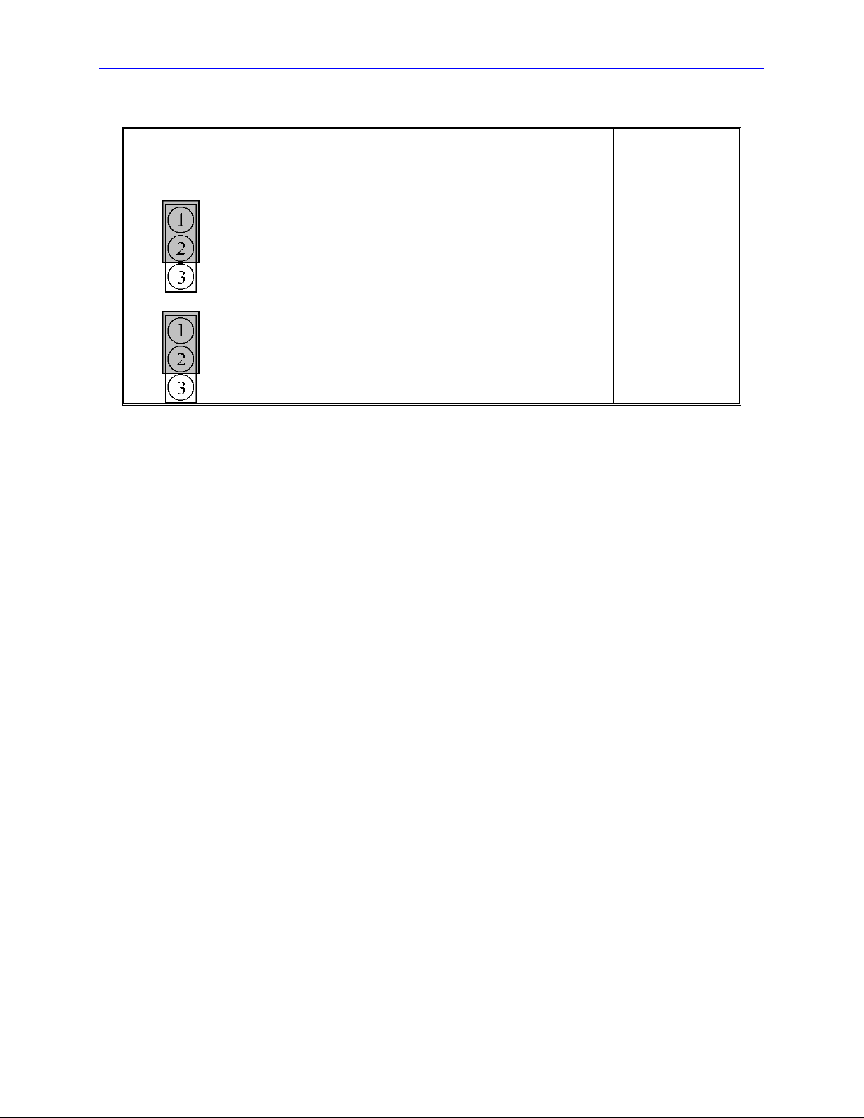
PMAC-PCI Hardware Reference
E121 - E122: XIN Feature Selection
E Point and
Physical
Layout
E121
Location Description Default
F1 Jump 1-2 to bring the QuadLoss signal for
Encoder 7 into register XIN6 at Y:$E801 bit 6.
Jump 2-3 to bring the QuadLoss signal for
Encoder 6 into register XIN6 at Y:$E801 bit 6.
1-2 Jumper
installed
E122
F1 Jump 1-2 to bring the PowerGood signal into
register XIN7 at Y:$E801 bit 7.
Jump 2-3 to bring the QuadLoss signal for
Encoder 8 into register XIN7 at Y:$E801 bit 7.
1-2 Jumper
installed
26 PMAC-PCI E-Point Jumper Descriptions
Page 37

PMAC-PCI Hardware Reference
MACHINE CONNECTIONS
Typically, the user connections are actually made to a terminal block that is attached to the JMACH
connector by a flat cable (Acc-8D or 8P). The pinout numbers on the terminal block are the same as
those on the JMACH connector. The possible choices for breakout boards are the following:
Board Mounting Breakout Style Breakout Connector Notes
Acc-8P DIN – Rail Monolithic Terminal Block Simple Phoenix contact board
Acc-8D DIN – Rail Monolithic Terminal Block
Acc-8DCE DIN – Rail Modular D-sub connector
Acc-8DP Panel Modular D-sub connector Used in the PC-pack product
Mounting
The PMAC PCI can be mounted in one of two ways: in the PCI bus, or using standoffs.
PCI bus: To mount in the PCI bus, simply insert the P1 card-edge connector into PCI socket. If there is a
standard PC-style housing, a bracket at the end of the PMAC PCI board can be used to screw into the
housing to hold the board down firmly.
• Standoffs: At each of the four corners of the PMAC PCI board, there are mounting holes that can be
used to mount the board on standoffs.
Headers for connection to option
boards
Fully shielded for easy CE mark
compliance
Power Supplies
Digital Power Supply
2A @ +5V (+/-5%) (10 W)
(Eight-channel configuration, with a typical load of encoders)
The host computer provides the 5 Volts power supply in the case PMAC is installed in its internal
•
bus.
With the board plugged into the bus, it will pull +5V power from the bus automatically and it cannot be
disconnected. In this case, there must be no external +5V supply or the two supplies will fight each other,
possibly causing damage. This voltage could be measured between pins 1 and 3 of the terminal block.
• In a stand-alone configuration, when PMAC is not plugged in a computer bus, it will need an external
five-volt supply to power its digital circuits. The +5V line from the supply should be connected to
pin 1 or 2 of the JMACH connector (usually through the terminal block), and the digital ground to pin
3 or 4. Acc-1x provides different options for the 5V power supply.
Analog Power Supply
0.3A @ +12 to +15V (4.5W)
0.25A @ -12 to -15V (3.8W)
(Eight-channel configuration)
The analog output circuitry on PMAC is optically isolated from the digital computation circuitry, and so
requires a separate power supply. This is brought in on the JMACH connector. The positive supply –
+12V to +15V – should be brought in on the A+15V line on pin 59. The negative supply – 12 to -15V –
should be brought in on the A-15V line on pin 60. The analog common should be brought in on the
AGND line on pin 58.
Machine Connection 27
Page 38
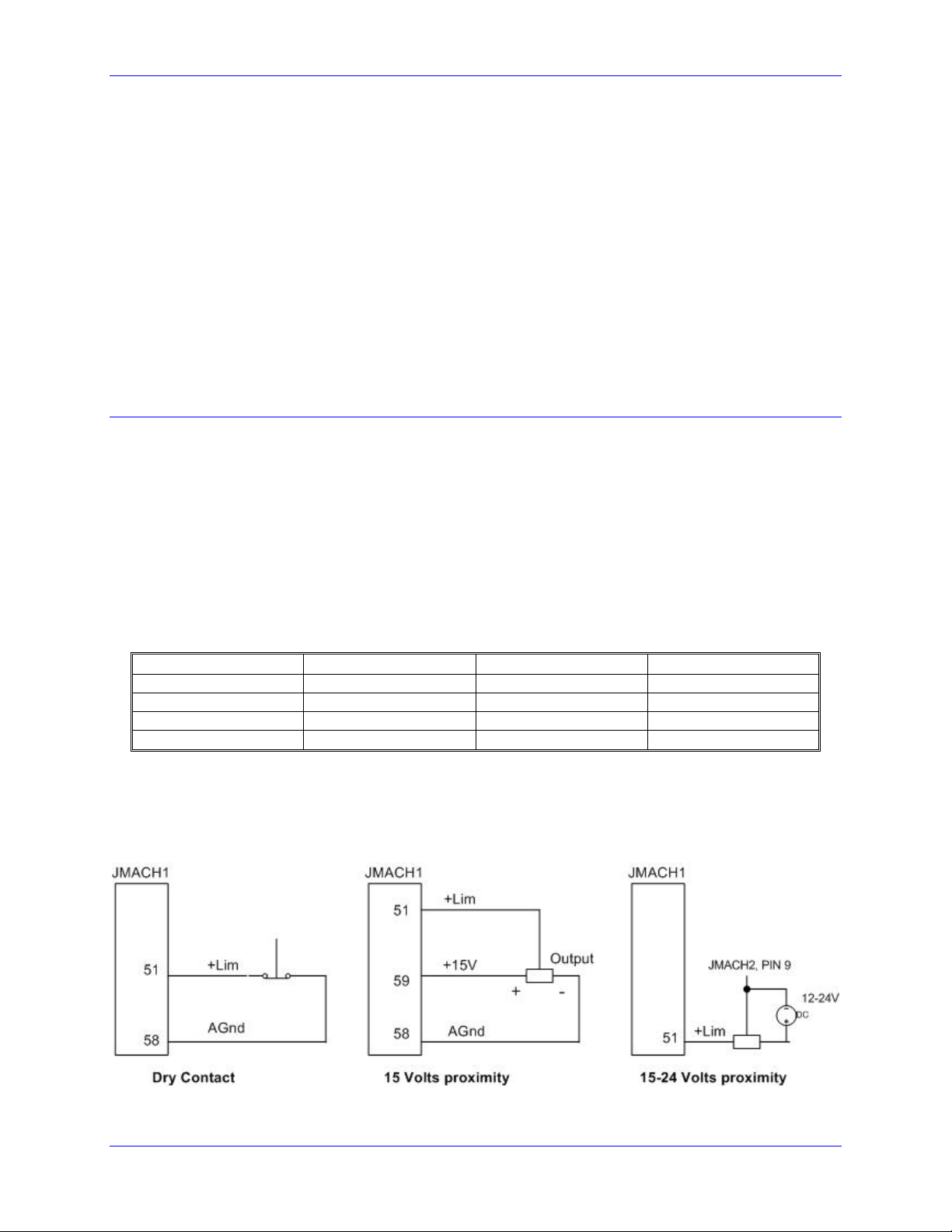
PMAC-PCI Hardware Reference
Typically, this supply can come from the servo amplifier; many commercial amplifiers provide such a
supply. If this is not the case, an external supply may be used. Acc-2x provides different options for the
± 15V power supply. Even with an external supply, the AGND line should be tied to the amplifier
common. It is possible to get the power for the analog circuits from the bus, but doing so defeats optical
isolation. In this case, no new connections need to be made. However, you should be sure jumpers E85,
E87, E88, E89, and E90 are set up for this circumstance. (The card is not shipped from the factory in this
configuration.)
Flags Power Supply (optional)
Each channel of PMAC has four dedicated digital inputs on the machine connector: +LIMn, -LIMn
(overtravel limits), HMFLn (home flag), and FAULTn (amplifier fault). If the PMAC is ordered with the
Option-1 (8-axis PMAC), these inputs can be kept isolated from other circuits. A power supply from 12
to 24V connected on pin 59 of J7 could be used to power the corresponding opto-isolators. In this case,
jumper E89 must be removed and jumper E90 must connect pins 1-2.
Overtravel Limits and Home Switches
When assigned for the dedicated uses, these signals provide important safety and accuracy functions.
+LIMn and -LIMn are direction-sensitive overtravel limits that must be actively held low (sourcing
current from the pins to ground) to permit motion in their direction. The direction sense of +LIMn and LIMn is as follows: +LIMn should be placed at the negative end of travel, and -LIMn should be placed at
the positive end of travel.
Resistor Pack Configuration: Flag and Digital Inputs Voltage Selection
The PMAC PCI is provided with 6-pin sockets for SIP resistor packs for the input flag sets. Each PMAC
PCI is shipped with no resistor packs installed. If the flag or digital inputs circuits are in the 12V to 24V
range, no resistor pack should be installed in these sockets. For flags or digital inputs at 5V levels, quad
1kΩ SIP resistor packs (1KSIP6C) should be installed in these sockets. The following table lists the
voltage selection resistor pack sockets for each input device:
Device Resistor Pack Device Resistor Pack
Flags 1 RP77 Flags 5 RP113
Flags 2 RP83 Flags 6 RP119
Flags 3 RP89 Flags 7 RP125
Flags 4 RP94 Flags 8 RP130
Types of Overtravel Limits
PMAC expects a closed-to-ground connection for the limits to not be considered on fault. This
arrangement provides a failsafe condition and therefore it cannot be reconfigured differently in PMAC.
Usually a passive normally close switch is used. If a proximity switch is needed instead, use a 15V
normally closed to ground NPN sinking type sensor.
Jumper E89, E90 and E100 must be set appropriately for the type of sensor used.
28 Machine Connection
Page 39

PMAC-PCI Hardware Reference
Home Switches
While normally closed-to-ground switches are required for the overtravel limits inputs, the home switches
could be either normally close or normally open types. The polarity is determined by the home sequence
setup, through the I-variables I902, I907, ... I977. However, for the following reasons, the same type of
switches used for overtravel limits are recommended:
Normally closed switches are proven to have greater electrical noise rejection than normally open types.
Using the same type of switches for every input flag simplifies maintenance stock and replacements.
Motor Signals Connections (JMACH Connectors)
Resistor Pack Configuration: Termination Resistors
The PMAC PCI provides sockets for termination resistors on differential input pairs coming into the
board. As shipped, there are no resistor packs in these sockets. If these signals are brought long distances
into the PMAC PCI board and ringing at signal transitions is a problem, SIP resistor packs may be
mounted in these sockets to reduce or eliminate the ringing.
All termination resistor packs are the type that has independent resistors (no common connection) with
each resistor using 2 adjacent pins. The following table shows which packs are used to terminate each
input device:
Device Resistor Pack Pack Size Device Resistor Pack Pack Size
Encoder 1 RP61 6-pin Encoder 5 RP98 6-pin
Encoder 2 RP63 6-pin Encoder 6 RP100 6-pin
Encoder 3 RP67 6-pin Encoder 7 RP104 6-pin
Encoder 4 RP69 6-pin Encoder 8 RP106 6-pin
Resistor Pack Configuration: Differential or Single-Ended Encoder
Selection
The differential input signal pairs to the PMAC PCI have user-configurable pull-up/pull-down resistor
networks to permit the acceptance of either single-ended or differential signals in one setting, or the
detection of lost differential signals in another setting.
The ‘+’ inputs of each differential pair each have a hard-wired 1 kΩ pull-up resistor to +5V. This cannot
be changed.
The ‘-‘ inputs of each differential pair each have a hard-wired 2.2 kΩ resistor to +5V; each also has
another 2.2 kΩ resistor as part of a socketed resistor pack that can be configured as a pull-up resistor to
+5V, or a pull-down resistor to GND.
If this socketed resistor is configured as a pull-down resistor (the default configuration), the combination
of pull-up and pull-down resistors on this line acts as a voltage divider, holding the line at +2.5V in the
absence of an external signal. This configuration is required for single-ended inputs using the ‘+’ lines
alone; it is desirable for unconnected inputs to prevent the pick-up of spurious noise; it is permissible for
differential line-driver inputs.
If this socketed resistor is configured as a pull-up resistor (by reversing the SIP pack in the socket), the
two parallel 2.2 kΩ resistors act as a single 1.1 kΩ pull-up resistor, holding the line at +5V in the absence
of an external signal. This configuration is required if encoder-loss detection is desired; it is required if
complementary open-collector drivers are used; it is permissible for differential line-driver inputs even
without encoder loss detection.
Machine Connection 29
Page 40
PMAC-PCI Hardware Reference
If Pin 1 of the resistor pack, marked by a dot on the pack, matches Pin 1 of the socket, marked by a wide
white line on the front side of the board, and a square solder pin on the back side of the board, then the
pack is configured as a bank of pull-down resistors. If the pack is reversed in the socket, it is configured
as a bank of pull-up resistors.
The following table lists the pull-up/pull-down resistor pack for each input device:
Device Resistor Pack Pack Size Device Resistor Pack Pack Size
Encoder 1 RP60 6-pin Encoder 5 RP97 6-pin
Encoder 2 RP62 6-pin Encoder 6 RP99 6-pin
Encoder 3 RP66 6-pin Encoder 7 RP103 6-pin
Encoder 4 RP68 6-pin Encoder 8 RP105 6-pin
Incremental Encoder Connection
Each JMACH connector provides two +5V outputs and two logic grounds for powering encoders and
other devices. The +5V outputs are on pins 1 and 2; the grounds are on pins 3 and 4. The encoder signal
pins are grouped by number: all those numbered 1 (CHA1, CHA1/, CHB1, CHC1, etc.) belong to encoder
#1. The encoder number does not have to match the motor number, but usually does. If the PMAC is not
plugged into a bus and drawing its +5V and GND from the bus, use these pins to bring in +5V and GND
from the power supply. Connect the A and B (quadrature) encoder channels to the appropriate terminal
block pins. For encoder 1, the CHA1 is pin 25, CHB1 is pin 21. If using a single-ended signal, leave the
complementary signal pins floating – do not ground them. However, if single-ended encoders are used,
please check the settings of the jumpers E18 to E21 and E24 to E27. For a differential encoder, connect
the complementary signal lines – CHA1/ is pin 27, and CHB1/ is pin 23. The third channel (index pulse)
is optional; for encoder 1, CHC1 is pin 17, and CHC1/ is pin 19.
Example: differential quadrature encoder connected to channel #1:
DAC Output Signals
If PMAC is not performing the commutation for the motor, only one analog output channel is required to
command the motor. This output channel can be either single-ended or differential, depending on what
the amplifier is expecting. For a single-ended command using PMAC channel 1, connect DAC1 (pin 43)
to the command input on the amplifier. Connect the amplifier’s command signal return line to PMAC's
AGND line (pin 58). In this setup, leave the DAC1/ pin floating; do not ground it.
For a differential command using PMAC Channel 1, connect DAC1 (pin 43) to the plus command input
on the amplifier. Connect DAC1/ (pin 45) to the minus-command input on the amplifier. PMAC’s
AGND should still be connected to the amplifier common. If the amplifier is expecting separate sign and
magnitude signals, connect DAC1 (pin 43) to the magnitude input. Connect AENA1/DIR1 (pin 47) to the
sign (direction input). Amplifier signal returns should be connected to AGND (pin 58). This format
requires some parameter changes on PMAC; (see Ix25. Jumper E17 controls the polarity of the direction
output; this may have to be changed during the polarity test.
30 Machine Connection
Page 41

PMAC-PCI Hardware Reference
This magnitude-and-direction mode is suited for driving servo amplifiers that expect this type of input,
and for driving voltage-to-frequency (V/F) converters, such as PMAC’s Acc-8D Option 2 board, for
running stepper motor drivers.
If you are using PMAC to commutate the motor, you will use two analog output channels for the motor.
Each output may be single-ended or differential, just as for the DC motor. The two channels must be
consecutively numbered, with the lower-numbered channel having an odd number (e.g. you can use
DAC1 and DAC2 for a motor, or DAC3 and DAC4, but not DAC2 and DAC3, or DAC2 and DAC4). For
our motor #1 example, connect DAC1 (pin 43) and DAC2 (pin 45) to the analog inputs of the amplifier. If
using the complements as well, connect DAC1/ (pin 45) and DAC2/ (pin 46) the minus-command inputs;
otherwise leave the complementary signal outputs floating. If you need to limit the range of each signal
to +/- 5V, you will do so with parameter Ix69. Any analog output not used for dedicated servo purposes
may be utilized as a general-purpose analog output. Usually this is done by defining an M-variable to the
digital-to-analog-converter register (suggested M-variable definitions M102, M202, etc.), then writing
values to the M-variable. The analog outputs are intended to drive high-impedance inputs with no
significant current draw. The 220Ω output resistors will keep the current draw lower than 50 mA in all
cases and prevent damage to the output circuitry, but any current draw above 10 mA can result in
noticeable signal distortion.
Example:
Amplifier Enable Signal (AENAx/DIRn)
Most amplifiers have an enable/disable input that permits complete shutdown of the amplifier regardless
of the voltage of the command signal. PMAC’s AENA line is meant for this purpose. If not using a
direction and magnitude amplifier or voltage-to-frequency converter, you can use this pin to enable and
disable your amplifier (wired to the enable line). AENA1/DIR1 is pin 47. This signal is an opencollector output with a 3.3 kΩ pull-up resistor to +V, which is a voltage selected by jumper E100. The
pull-up resistor packs are RP43 for channels 1-4 and RP-56 for motors 5-8. For early tests, you may wish
to have this amplifier signal under manual control.
This signal could be either sinking or sourcing as determined by chips U37 and U53 (see jumpers E100E102 and E114-E115). For 24V operation, E100 must connect pins 2-3 and a separate power supply must
be brought on pins 9-7 of the J9 JEQU connector. The polarity of the signal is controlled by jumpers
E17A to E17H. The default is low-true (conducting) enable. The amplifier enable signal could also be
manually controlled setting Ix00=0 and using the suggested definition of the Mx14 variable.
Machine Connection 31
Page 42

PMAC-PCI Hardware Reference
Amplifier Fault Signal (FAULTn)
This input can take a signal from the amplifier so PMAC knows when the amplifier is having problems,
and can shut down action. The polarity is programmable with I-variable Ix25 (I125 for motor #1) and the
return signal is analog ground (AGND). FAULT1 is pin 49. With the default setup, this signal must
actively be pulled low for a fault condition. In this setup, if nothing is wired into this input, PMAC will
consider the motor not to be in a fault condition. The amplifier fault signal could be monitored using the
properly defined Mx23 variable.
Some amplifiers share the amplifier fault output with the amplifier enable\disable status output. In this
case, a special PLC code must be written with the following sequence: disable the amplifier fault input
(see Ix25), enable the motor (J/ command), wait for the amplifier fault input to be false (monitor Mx23),
re-enable the amplifier fault input (see Ix25).
General-Purpose Digital Inputs and Outputs (JOPTO Port)
PMAC’s J5 or JOPTO connector provides eight general-purpose digital inputs and eight general-purpose
digital outputs. Each input and each output has its own corresponding ground pin in the opposite row.
The 34-pin connector was designed for easy interface to OPTO-22 or equivalent optically isolated I/O
modules. Delta Tau’s Acc-21F is a six-foot cable for this purpose. Characteristics of the JOPTO port on
the PMAC PCI:
• 16 I/O points. 100 mA per channel, up to 24V
• Hardware selectable between sinking and sourcing in groups of eight; default is all sinking (inputs
can be changed simply by moving a jumper; sourcing outputs must be special-ordered or fieldconfigured)
• Eight inputs, eight outputs only; no changes. Parallel (fast) communications to PMAC CPU
• Not opto-isolated; easily connected to Opto-22 (PB16) or similar modules through Acc-21F cable
Jumper E7 controls the configuration of the eight inputs. If it connects pins 1 and 2 (the default setting), the
inputs are biased to +5V for the off state, and they must be pulled low for the on state. If E7 connects pins 2
and 3, the inputs are biased to ground for the off state, and must be pulled high for the on state. In either case,
a high voltage is interpreted as a '0' by the PMAC software, and a low voltage is interpreted as a 1.
WARNING:
Having Jumpers E1 and E2 set wrong can damage the IC. The +V output on this
connector has a 2 A fuse, F1, for excessive current protection.
PMAC is shipped standard with a ULN2803A sinking (open-collector) output IC for the eight outputs.
These outputs can sink up to 100 mA and have an internal 3.3 kΩ pull-up resistor to go high (RP18).
32 Machine Connection
Page 43

PMAC-PCI Hardware Reference
Do not connect these outputs directly to the supply voltage, or damage to the PMAC will result from
excessive current draw. The user can provide a high-side voltage (+5 to +24V) into Pin 33 of the JOPTO
connector, and allow this to pull up the outputs by connecting pins 1 and 2 of Jumper E1. Jumper E2
must also connect pins 1 and 2 for a ULN2803A sinking output.
It is possible for these outputs to be sourcing drivers by substituting a UDN2981A IC for the ULN2803A.
This U13 IC is socketed, and so may easily be replaced. For this driver, the internal resistor packs pulldown instead. With a UDN2981A driver IC, Jumper E1 must connect pins 2 and 3, and Jumper E2 must
connect pins 2 and 3.
The outputs can be individually configured to a different output voltage by removing the internal pull-up
resistor pack RP18 and connecting to each output a separate external pull-up resistor to the desired
voltage level.
Example: Standard configuration using the ULN2803A sinking (open-collector) output IC
Control-Panel Port I/O (JPAN Port)
The J2 (JPAN) connector is a 26-pin connector with dedicated control inputs, dedicated indicator outputs,
a quadrature encoder input, and an analog input. The control inputs are low-true with internal pull-up
resistors. They have predefined functions unless the control-panel-disable I-variable (I2) has been set to
1. If this is the case, they may be used as general-purpose inputs by assigning M-variable to their
corresponding memory-map locations (bits of Y address $FFC0).
Command Inputs
JOG-/, JOG+/, PREJ/ (return to pre-jog position), and HOME/ affect the motor selected by the FDPn/
lines (see below). The ones that affect a coordinate system are STRT/ (run), STEP/, STOP/ (abort), and
HOLD/ (feed hold) affect the coordinate system selected by the FDPn/ lines.
Selector Inputs
The four low-true BCD-coded input lines FDP0/ (LSBit), FDP1/, FDP2/, and FDP3/ (MSBit) form a lowtrue BCD-coded nibble that selects the active motor and coordinate system (simultaneously). These are
usually controlled from a single 4-bit motor/coordinate-system selector switch. The motor selected with
these input lines will respond to the motor-specific inputs. It will also have its position following
function turned on (Ix06 is set to 1 automatically); the motor just de-selected has its position following
function turned off (Ix06 is set to 0 automatically).
It is not a good idea to change the selector inputs while holding one of the jog inputs low. Releasing the
jog input will then not stop the previously selected motor. This can lead to a dangerous situation.
Alternate Use
The discrete inputs can be used for parallel-data servo feedback or master position if I2 has been set to 1.
The Acc-39 Handwheel Encoder Interface board provides 8-bit parallel counter data from a quadrature
encoder to these inputs. Refer to the Acc-39 manual and Parallel Position Feedback Conversion under
Setting up a Motor for more details on processing this data.
Machine Connection 33
Page 44

PMAC-PCI Hardware Reference
Reset Input
Input INIT/ (reset) affects the entire card. It has the same effect as cycling power or a host $$$
command. It is hard-wired, so it retains its function even if I2 is set to 1.
Handwheel Inputs
The handwheel inputs HWCA and HWCB can be connected to the second encoder counter on PMAC
with jumpers E22 and E23. If these jumpers are on, nothing else should be connected to the Encoder 2
inputs. The signal can be interpreted either as quadrature or as pulse (HWCA) and direction (HWCB),
depending on the value of I905. I905 also controls the direction sense of this input. Make sure that the
Encoder 2 jumper E26 is set for single ended signals, connecting pins 1 and 2.
Optional Voltage to Frequency Converter
The WIPER analog input (0 to +10V on PMAC PCI referenced to digital ground) provides an input to a
voltage-to-frequency converter (V/F) with a gain of 25 kHz/Volt, providing a range of 0-250 kHz. The
output of the V/F can be connected to the Encoder 4 counter using jumpers E72 and E73. If these
jumpers are on, nothing else should be connected to the Encoder 4 inputs. Make sure that the Encoder 4
jumper E24 is set for single-ended signals, connecting pins 1 and 2. This feature requires the ordering of
Option-15.
Frequency Decode: When used in this fashion, Encoder 4 must be set up for pulse-and-direction decode
by setting I915 to 0 or 4. A value of 4 is usually used, because with CHB4 (direction) unconnected, a
positive voltage causes the counter to count up. The encoder conversion table can then take the difference
in the counter each servo cycle and scale it, providing a value proportional to frequency, and therefore to
the input voltage. Usually this is used for feedrate override (time base control), but the resulting value
can be used for any purpose. The resulting value in the default setup can be found at X:$729,24
Power Supply: For the V/F converter to work, PMAC must have +/-12V supply referenced to digital
ground. If PMAC is in a bus configuration, this usually comes through the bus connector from the bus
power supply. In a standalone configuration, this supply must still be brought through the bus connector
(or the supply terminal block), or it must be jumpered over from the analog side with E85, E87, and E88,
defeating the optical isolation on the board.
(Optional user
provided +10V)
-5Kohm
+5V
Wiper
GND
J2
25
20
26
Using PMAC’s Control Panel
Analog (Wiper) Input
Voltage
0 to +10V
V/F
25 KHz/V
Hardware Voltage-toFrequency Converter
Pulse Train
0 to 250 KHz
E72
E73
(E24:1-2)
CHA4
ENC4
Decoder/
Counter
CHA4/
I915=4
Software-Configured
Hardware Counter
Integer
Count
24
X:$C00C+
Interpolated
1/T
Encoder
Conversion
Y:$723=$00C00C
Software
Interpolation
Count
24
X:$723
Proportional
to Voltage
“Time
Base”
Conversion
Y:$728=$400723
Y:$729=Scaling
Software
Differentiation
Value
24
X:$729
To use this value for feedrate override for a coordinate system, set the
time base source address I-Variable (Ix93 for C.S.x.) to 1833 ($729).
To use this value for some other purpose, assign an M-Variable to this
register (e.g., M60->X:$729,0-24-,U).
Scaling is set by the value in Y:$729 (for the default conversion table).
This value can be determined interactively by varying the input voltage
and noting the effect.
34 Machine Connection
Page 45

PMAC-PCI Hardware Reference
Thumbwheel Multiplexer Port (JTHW Port)
The Thumbwheel Multiplexer Port, or Multiplexer Port, on the JTHW (J3) connector has eight input lines
and eight output lines. The output lines can be used to multiplex large numbers of inputs and outputs on
the port, and Delta Tau provides accessory boards and software structures (special M-variable definitions)
to capitalize on this feature. Up to 32 of the multiplexed I/O boards may be daisy-chained on the port, in
any combination.
The Acc-18 Thumbwheel Multiplexer board provides up to 16 BCD thumbwheel digits or 64 discrete
TTL inputs per board. The TWD and TWB forms of M-variables are used for this board. The Acc-34x
family Serial I/O Multiplexer boards provide 64 I/O point per board, optically isolated from PMAC. The
TWS form of M-variables is used for these boards. The Acc-8D Option 7 Resolver-to-Digital Converter
board provides up to four resolver channels whose absolute positions can be read through the thumbwheel
port. The TWR form of M-variables is used for this board. The Acc-8D Option 9 Yaskawa
Encoder Interface board can connect to up to four of these encoders. The absolute position is read serially
through the multiplexer port on power up.
If none of these accessory boards is used, the inputs and outputs on this port may be used as discrete, nonmultiplexed I/O. They map into PMAC’s processor space at Y address $FFC1. The suggested Mvariable definitions for this use are M40 to M47 for the eight outputs, and M50 to M57 for the eight
inputs. The Acc-27 Optically Isolated I/O board buffers the I/O in this non-multiplexed form, with each
point rated to 24V and 100 mA.
TM
Absolute
Optional Analog Inputs (JANA Port)
The JANA port is present only if Option 12 is ordered for the PMAC PCI. Option 12 provides eight 12bit analog inputs (ANAI00-ANAI07). Option 12A provides eight additional 12-bit analog inputs
(ANA08-ANAI15) for a total of 16 inputs. The analog inputs can be used as unipolar inputs in the 0V to
+5V range, or bi-polar inputs in the -2.5V to +2.5V range.
The analog-to-digital converters on PMAC require +5V and -12V supplies. These supplies are not
isolated from digital +5V circuitry on PMAC. If the PMAC is plugged into the PCI bus, these supplies
are taken from the bus power supply. In a standalone application, these supplies must be brought in on
terminal block TB1. The -12V and matching +12V supply voltages are available on the J30 connector to
supply the analog circuitry providing the signals.
Only one pair of analog-to-digital converter registers is available to the PMAC processor at any given
time. The data appears to the processor at address Y:$FFC8. The data from the selected analog input 0 to
7 (ANAI00-ANAI07) appears in the low 12 bits; the data from the selected analog input 8 to 15
(ANAI08-ANAI15) appears in the high 12 bits (this data is only present if Option 12A has been ordered).
The input is selected and the conversion is started by writing to this same word address Y:$FFC8. A
value of 0 to 7 written into the low 12 bits selects the analog input channel of that number (ANAI00ANAI07) to be converted in unipolar mode (0V to +5V). A value of 0 to 7 written into the high 12 bits
selects the analog input channel numbered 8 greater (ANAI08-ANAI15) in unipolar mode. If the value
written into either the low 12 bits or the high 12 bits is 8 higher (8 to 15), the same input channel is
selected, but the conversion is in bipolar mode (-2.5V to +2.5V).
PMAC variables I60 and I61 allows an automatic conversion of the analog inputs. Setting I60=$FFC8
and I61 with the number of converted registers desired minus 1, the converted data can be found in
registers $0708 to $070F. See the PMAC Software Reference for further details on this.
Machine Connection 35
Page 46

PMAC-PCI Hardware Reference
Compare Equal Outputs Port (JEQU Port)
The compare-equals (EQU) outputs have a dedicated use of providing a signal edge when an encoder
position reaches a pre-loaded value. This is useful for scanning and measurement applications.
Instructions for use of these outputs are covered in detail in the PMAC’s User Manual.
Outputs can be configured sinking or sourcing by replacing the chips U37 or U53 and configuring the
jumpers E101-102 or E114-E115. The voltage levels can be individually configured by removing resistor
packs RP43 or RP56 and connecting an external pull-up resistor in each output to the desired voltage
level.
Serial Port (JRS422 Port)
For serial communications, use a serial cable to connect your PC’s COM port to the PMAC’s J4 serial
port connector. Delta Tau provides the Acc-3D cable that connects the PMAC PCI to a DB-25 connector.
Standard DB-9-to-DB-25 or DB-25-to-DB-9 adapters may be needed for a particular setup. Jumper E110
selects between RS-232 and RS422 signals type for the J4 connector. If a cable needs to be made, the
easiest approach is to use a flat cable prepared with flat-cable type connectors as indicated in the
following diagram:
36 Machine Connection
Page 47

PMAC-PCI Hardware Reference
Machine Connections Example
Machine Connection 37
Page 48

PMAC-PCI Hardware Reference
38 Machine Connection
Page 49

PMAC-PCI Hardware Reference
MATING CONNECTORS
This section lists several options for each connector. Choose an appropriate one for your application.
(See attached PMAC mating connector sketch for typical connection)
Base Board Connectors
J1 (JDISP)/Display
1. Two 14-pin female flat cable connector Delta Tau P/N 014-R00F14-0K0, T&B Ansley P/N 609-1441
2. 171-14 T&B Ansley standard flat cable stranded 14-wire
3. Phoenix varioface modules type FLKM14 (male pins) P/N 22 81 02 1
J2 (JPAN)/Control Panel
1. Two 26-pin female flat cable connector Delta Tau P/N 014-R00F26-0K0, T&B Ansley P/N 609-2641
2. 171.26.T&B Ansley standard flat cable stranded 26-wire
3. Phoenix varioface module type FLKM 26 (male pins) P/N 22 81 05 0
J3 (JTHW)/Multiplexer Port
1. Two 26-pin female flat cable connector Delta Tau P/N 014-R00F26-0K0, T&B Ansley P/N 609-2641
2. 171-26 T&B Ansley standard flat cable stranded 26-wire
3. Phoenix varioface module type FLKM 26 (male pins) P/N 22 81 05 0
J4 (JRS422)/RS232 or 422/Serial Communications
1. Two 26-pin female flat cable connector Delta Tau P/N 014-R00F26-0K0, T&B Ansley P/N 609-2641
2. 171-26 T&B Ansley standard flat cable stranded 26-wire
3. Phoenix varioface module type FLKM 26 (male pins) P/N 22 81 05 0
J5 (JOPT)/OPTO I/O
1. Two 34-pin female flat cable connector Delta Tau P/N 014-R00F34-0k0, T&B Ansley P/N 609-3441
2. 171-34 T&B Ansley standard flat cable stranded 34-wire
3. Phoenix varioface module type FLKM 34 (male pins) P/N 22 81 06 3
J6 (JXIO)/Expansion Board
1. Two 10-pin female flat cable connector Delta Tau P/N 014-R00F10-0K0, T&B Ansley P/N 609-1041
2. 171-10 T&B Ansley standard flat cable stranded 10-wire
3. Phoenix varioface module type FLKM 10 (male pins) P/N 22 81 01 8
J7 (JMACH2)/2nd Machine Connector (Option 1 Required)
1. Two 60-pin female flat cable connector Delta Tau P/N 014-R00F60-0K0, T&B Ansley P/N 609-6041
available as Acc-8P or 8D
2. 171-60 T&B Ansley standard flat cable stranded 60-wire
3. Phoenix varioface module type FLKM 60 (male pins) P/N 22 81 09 2
Note:
Normally, J7 and J8 are used with Accessory 8P or 8D with Option P, which
provides complete terminal strip fan-out of all connections.
J8 (JMACH1)/1st Machine Connector
1. Two 60-pin female flat cable connector Delta Tau P/N 014-R00F60-0K0, T&B Ansley P/N 609-6041
available as Acc-8P or 8D
2. 171-60 T&B Ansley standard flat cable stranded 60-wire
3. Phoenix varioface module type FLKM 60 (male pins) P/N 22 81 09 2
Mating Connectors 39
Page 50

PMAC-PCI Hardware Reference
Note:
Normally, J7 and J8 are used with Acc-8P or 8D with Option P, which provides
complete terminal strip fan-out of all connections.
JS1/A-D Inputs 1-4
1. Two 16-pin female flat cable connector Delta Tau P/N 014-R00F16-0K0, T&B Ansley P/N 609-1641
2. 171-16 T&B Ansley standard flat cable stranded 16-wire
3. Phoenix varioface module type FLKM 16 (male pins) P/N 22 81 03 4
JS2/A-D Inputs 5-8 (Option 1 Required)
1. Two 16-pin female flat cable connector Delta Tau P/N 014-R00F16-0K0, T&B Ansley P/N 609-1641
2. 171-16 T&B Ansley standard flat cable stranded 16-wire
3. Phoenix varioface module type FLKM 16 (male pins) P/N 22 81 03 4
JEQU/Position Compare
1. Two 10-pin female flat cable connector Delta Tau P/N 014-R00F10-0K0, T&B Ansley P/N 609-1041
2. 171-10 T&B Ansley standard flat cable stranded 10-wire
3. Phoenix varioface module type FLKM 10 (male pins) P/N 22 81 01 8
JANA/Analog Inputs Option
1. Two 20-pin female flat cable connector Delta Tau P/N 014-R00F20-0K0, T&B Ansley P/N 609-2041
2. 171-20 T&B Ansley standard flat cable stranded 20-wire
3. Phoenix varioface modules type FLKM20 (male pins)
CPU Board Connectors
J2 (JEXP)/Expansion
1. Two 50-pin female flat cable connector Delta Tau P/N 014-R00F50-0K0, T&B Ansley P/N 609-5041
2. 171-50 T&B Ansley standard flat cable stranded 50-wire
3. Phoenix varioface module type FLKM 50 (male pins) P/N 22 81 08 9 used for daisy chaining acc-14
I/0, -23 A and D connectors -24 expansion
J4 (JDPRAM)/Dual-Ported RAM
1. Two 10-pin female flat cable connector Delta Tau P/N 014-R00F10-0K0, T&B Ansley P/N 609-1041
2. 171-10 T&B Ansley standard flat cable stranded 10-wire
3. Phoenix varioface module type FLKM 10 (male pins) P/N 22 81 01 8
40 Mating Connectors
Page 51

PMAC-PC Hardware Reference
BASE BOARD CONNECTOR PINOUTS
J1: Display Port Connector
J1 JDISP (14-Pin Connector)
Front View
Pin # Symbol Function Description Notes
1 Vdd Output +5V Power Power supply out
2 Vss Common PMAC Common
3 Rs Output Read Strobe TTL signal out
4 Vee Output Contrast Adjust VEE 0 TO +5 VDC *
5 E Output Display Enable High is enable
6 R/W Output Read or Write TTL signal out
7 DB1 Output Display Data 1
8 DB0 Output Display Data 0
9 DB3 Output Display Data 3
10 DB2 Output Display Data 2
11 DB5 Output Display Data 5
12 DB4 Output Display Data 4
13 DB7 Output Display Data 7
14 DB6 Output Display Data 6
* Controlled by potentiometer R1
The JDISP connector is used to drive the 2-line x 24-character (Acc-12), 2 x 40 (Acc-12A) LCD, or the 2
x 40 vacuum fluorescent (Acc 12C) display unit. The DISPLAY command may be used to send messages
and values to the display.
See Also:
Program Commands: Display
Accessories; Acc-12, 12A, 12C, Acc-16D
Memory Map: Y:$0780 - $07D1
PMAC-PCI Base Board Connector Pinouts 41
Page 52

PMAC-PC Hardware Reference
J2: Control Panel Port Connector
J2 JPAN (26-Pin Connector)
Front View
Pin # Symbol Function Description Notes
1 +5V Output +5V Power For remote panel
2 GND Common PMAC Common
3 FPD0/ Input Motor/C.S. Select Bit 0 Low is TRUE
4 JOG-/ Input Job In - DIR. Low is JOG -
5 FPD1/ Input Motor/C.S. Select Bit 1 Low is TRUE
6 JOG+/ Input Jog In + DIR. Low is JOG +
7 PREJ/ Input Return to PreJog Position Low is RETURN
Equiv to J= CMD
8 STRT/ Input Start Program Run Low is START
Equiv to R CMD
9 STEP/ Input Step Through Program Low is STEP
Equiv to S OR Q
10 STOP/ Input Stop Program Run Low is STOP
Equiv to A
11 HOME/ Input Home Search Command Low is GO HOME
Equiv to HM
12 HOLD/ Input Hold Motion Low is HOLD
Equiv to H
13 FPD2/ Input Motor/C.S. Select Bit 2 Low is TRUE
14 FPD3/ Input Motor/C.S. Select Bit 3 Low is TRUE
15 INIT/ Input Reset PMAC Low is RESET
Equiv to "$$$"
16 HWCA Input Handwheel Enc. A Channel 5V TTL sq. pulse must
use E23 (CHA2)
17 IPLD/ Output In Position Ind. (C.S.) Low lights LED
18 BRLD/ Output Buffer Request Ind. Low lights LED
19 ERLD/ Output Fatal Follow Err (C.S.) Low lights LED
20 WIPER Input Feed Pot Wiper 0 to +10V input must use
E72, E73 (CHA4)
21 (SPARE) N.C.
22 HWCB Input Handwheel Enc. B Channel 5V TTL sq. pulse must
use E22 (CHB2)
23 F1LD/ Output Warn Follow Error (C.S.) Low lights LED
24 F2LD/ Output Watchdog Timer Low lights LED
25 +5V Output +5V Power For remote panel
26 GND Common PMAC Common
The JPAN connector can be used to connect the Accessory 16 (Control Panel), or customer-provided I/O,
to the PMAC, providing manual control of PMAC functions via simple toggle switches. If the automatic
control panel input functions are disabled (I2=1), the inputs become general-purpose TTL inputs, and the
coordinate system (C.S.) specific outputs pertain to the host-addressed coordinate system.
See Also:
Control panel inputs, Accessories: Acc-16, Acc-39
I-variables: I2, Ix06. I/O and Memory Map Y:$FFC0. Suggested M-variables M20 - M32
42 PMAC-PCI Base Board Connector Pinouts
Page 53

PMAC-PC Hardware Reference
J3: Multiplexer Port Connector
J3 JTHW (26-Pin Connector)
Front View
Pin # Symbol Function Description Notes
1 GND Common PMAC Common
2 GND Common PMAC Common
3 DAT0 Input Data-0 Input Data input from multiplexed accessory
4 SEL0 Output Select-0 Output Multiplexer select output
5 DAT1 Input Data-1 Input Data input from multiplexed accessory
6 SEL1 Output Select-1 Output Multiplexer select output
7 DAT2 Input Data-2 Input Data input from multiplexed accessory
8 SEL2 Output Select-2 Output Multiplexer select output
9 DAT3 Input Data-3 Input Data input from multiplexed accessory
10 SEL3 Output Select-3 Output Multiplexer select output
11 DAT4 Input Data-4 Input Data input from multiplexed accessory
12 SEL4 Output Select-4 Output Multiplexer select output
13 DAT5 Input Data-5 Input Data input from multiplexed accessory
14 SEL5 Output Select-5 Output Multiplexer select output
15 DAT6 Input Data-6 Input Data input from multiplexed accessory
16 SEL6 Output Select-6 Output Multiplexer select output
17 DAT7 Input Data-7 Input Data input from multiplexed accessory
18 SEL7 Output Select-7 Output Multiplexer select output
19 N.C. N.C. No Connection
20 GND Common PMAC Common
21 BRLD/ Output Buffer Request Low is Buffer Request
22 GND Common PMAC Common
23 IPLD/ Output In Position Low is In Position
24 GND Common PMAC Common
25 +5V Output +5VDC Supply Power supply out
26 INIT/ Input PMAC Reset Low is reset
The JTHW multiplexer port provides eight inputs and eight outputs at TTL levels. While these I/O can be used in
un-multiplexed form for 16 discrete I/O points, most users will utilize PMAC software and accessories to use this
port in multiplexed form to greatly multiply the number of I/O that can be accessed on this port. In multiplexed
form, some of the SELn outputs are used to select which of the multiplexed I/O are to be accessed.
See also:
I/O and Memory Map Y:$FFC1
Suggested M-variables M40 - M58
M-variable formats TWB, TWD, TWR, TWS
Acc-8D Option 7, Acc-8D Option 9, Acc-18, Acc-34x, NC Control Panel
PMAC-PCI Base Board Connector Pinouts 43
Page 54

PMAC-PC Hardware Reference
J4: Serial Port Connector
J4 JRS422 (26-Pin Connector)
Front View
Pin # Symbol Function Description Notes
1 CHASSI Common PMAC Common
2 S+5V Output +5VDC Supply Deactivated by E8
3 RD- Input Receive Data Diff. I/O low TRUE **
4 RD+ Input Receive Data Diff. I/O high TRUE *
5 SD- Output Send Data Diff. I/O low TRUE **
6 SD+ Output Send Data Diff. I/O high TRUE *
7 CS+ Input Clear to Send Diff . I/O high TRUE **
8 CS- Input Clear to Send Diff. I/O low TRUE *
9 RS+ Output Req. to Send Diff. I/O high TRUE **
10 RS- Output Req. to Send Diff. I/O low TRUE *
11 DTR Bidirectional Data Terminal Ready Tied to DSR
12 INIT/ Input PMAC Reset Low is RESET
13 GND Common PMAC Common Low is RESET
14 DSR Bidirectional Data Set Ready Tied to DTR
15 SDIO- Bidirectional Special Data Diff. I/O low TRUE
16 SDIO+ Bidirectional Special Data Diff. I/O high TRUE
17 SCIO- Bidirectional Special CTRL. Diff I/O low TRUE
18 SCIO+ Bidirectional Special CTRL. Diff. I/O high TRUE
19 SCK- Bidirectional Special Clock Diff. I/O low TRUE
20 SCK+ Bidirectional Special Clock Diff. I/O high TRUE
21 SERVO- Bidirectional Servo Clock Diff. I/O low TRUE
22 SERVO+ Bidirectional Servo Clock Diff. I/O high TRUE ***
23 PHASE- Bidirectional Phase Clock Diff I/O low TRUE ***
24 PHASE+ Bidirectional Phase Clock Diff. I/O high TRUE ***
25 GND Common PMAC Common
26 +5V Output +5VDC Supply Power supply out
The JRS422 connector provides the PMAC with the ability to communicate both in RS422 and RS232. In
addition, this connector is used to daisy chain interconnect multiple PMACs for synchronized operation.
Jumper E110 selects between RS-232 or RS-422 signal types.
Jumper E110 enables or disables the use of the PHASE, SERVO and INIT lines
* Note: Required for communications to an RS-422 host port
** Note: Required for communications to an RS-422 or RS-232 host port
*** Note: Output on card @0; input on other cards. These pins are for synchronizing multiple PMACs
together by sharing their phasing and servo clocks. The PMAC designated as card 0 (@0) by its jumpers
E40-E43 outputs its clock signals. Other PMACs designated as cards 1-15 (@1-@F) by their jumpers
E40-E43 take these signals as inputs. If synchronization is desired, these lines should be connected even
if serial communications is not used.
See Also:
Serial Communications
Synchronizing PMAC to other PMACs
44 PMAC-PCI Base Board Connector Pinouts
Page 55

PMAC-PC Hardware Reference
J5: I/O Port Connector
J5 JOPT (34-Pin Connector)
Front View
Pin # Symbol Function Description Notes
1 MI8 Input Machine input 8 Low is TRUE
2 GND Common PMAC common
3 MI7 Input Machine input 7 Low is TRUE
4 GND Common PMAC common
5 MI6 Input Machine input 6 Low is TRUE
6 GND Common PMAC common
7 MI5 Input Machine input 5 Low is TRUE
8 GND Common PMAC common
9 MI4 Input Machine input 4 Low is TRUE
10 GND Common PMAC common
11 MI3 Input Machine input 3 Low is TRUE
12 GND Common PMAC common
13 MI2 Input Machine input 2 Low is TRUE
14 GND Common PMAC common
15 MI1 Input Machine input 1 Low is TRUE
16 GND Common PMAC common
17 MO8 Output Machine output 8 Low-TRUE (sinking);
High-TRUE (sourcing)
18 GND Common PMAC common
19 MO7 Output Machine output 7 " "
20 GND Common PMAC common
21 MO6 Output Machine output 6 " "
22 GND Common PMAC common
23 MO5 Output Machine output 5 " "
24 GND Common PMAC common
25 MO4 Output Machine output 4 " "
26 GND Common PMAC common
27 MO3 Output Machine output 3 " "
28 GND Common PMAC common
29 MO2 Output Machine output 2 " "
30 GND Common PMAC common
31 MO1 Output Machine output 1 " "
32 GND Common PMAC common
33 +V Input/
Output
34 GND Common PMAC common
This connector provides means for eight general-purpose inputs and eight general-purpose outputs. Inputs and
outputs may be configured to accept or provide either +5V or +24V signals. Outputs can be made sourcing
with an IC (U13 to UDN2981) and jumper (E1 & E2) change. E7 controls whether the inputs are pulled up or
down internally. Outputs are rated at 100mA per channel.
+V power I/O +V = +5V to +24V
+5V out from PMAC, +5 to +24V in
from external source, diode, isolation
from PMAC
PMAC-PCI Base Board Connector Pinouts 45
Page 56

PMAC-PC Hardware Reference
J6: Auxiliary I/O Port Connector
J6 JXIO (10-Pin Connector)
Front View
Pin # Symbol Function Description Notes
1 CHA1 Input Enc. A Chan. Pos. Axis #1 for resolver
2 CHB1 Input Enc. B Chan. Pos. Axis #1 for resolver
3 CHC1 Input Enc. C Chan. Pos. Axis #1 for resolver
4 CHA3 Input Enc. A Chan. Pos. Axis #3 for resolver
5 CHB3 Input Enc. B Chan. Pos. Axis #3 for resolver
6 CHC3 Input Enc. C Chan. Pos. Axis #3 for resolver
7 E63 Input Interrupt IR4 Interrupt from EXP board
8 E59 Input Interrupt IR5 Interrupt from EXP board
9 SCLK Output Encoder clock Encoder sample rate
10 DCLK Output D to A, A to D clock DAC and ADC clock for all channels
This connector is used for miscellaneous I/O functions related to expansion cards that are used with PMAC.
46 PMAC-PCI Base Board Connector Pinouts
Page 57

PMAC-PC Hardware Reference
J7: Machine Port 2 Connector
J7 JMACH2
(60-Pin Header)
Pin # Symbol Function Description Notes
1 +5V Output +5V Power For encoders, 1
2 +5V Output +5V Power For encoders, 1
3 GND Common Digital Common
4 GND Common Digital Common
5 CHC7 Input Encoder C Chan. Pos. 2
6 CHC8 Input Encoder C Chan. Pos. 2
7 CHC7/ Input Encoder Chan. Neg. 2,3
8 CHC8/ Input Encoder C Chan. Neg. 2,3
9 CHB7 Input Encoder B Chan. Pos. 2
10 CHB8 Input Encoder B Chan. Pos. 2
11 CHB7/ Input Encoder B Chan. Neg. 2,3
12 CHB8/ Input Encoder B Chan. Neg. 2,3
13 CHA7 Input Encoder A Chan. Pos. 2
14 CHA8 Input Encoder A Chan. Pos. 2
15 CHA7/ Input Encoder A Chan. Neg. 2,3
16 CHA8/ Input Encoder A Chan. Neg. 2,3
17 CHC5 Input Encoder C Chan. Pos. 2
18 CHC6 Input Encoder C Chan. Pos. 2
19 CHC5/ Input Encoder C Chan. Neg. 2,3
20 CHC6/ Input Encoder C Chan. Neg. 2,3
21 CHB5 Input Encoder B Chan. Pos. 2
22 CHB6 Input Encoder B Chan. Pos. 2
23 CHB5/ Input Encoder B Chan. Neg. 2,3
24 CHB6/ Input Encoder B Chan. Neg. 2,3
25 CHA5 Input Encoder A Chan. Pos. 2
26 CHA6 Input Encoder A Chan. Pos. 2
27 CHA5/ Input Encoder A Chan. Neg. 2,3
28 CHA6/ Input Encoder A Chan. Neg. 2,3
29 DAC7 Output Analog Out Pos. 7 4
30 DAC8 Output Analog Out Pos. 8 4
31 DAC7/ Output Analog Out Neg. 7 4,5
32 DAC8/ Output Analog Out Neg. 8 4,5
33 AENA7/DIR7 Output Amp-Enable/Dir. 7 6
34 AENA8/DIR8 Output Amp-Enable/Dir. 8 6
35 FAULT7 Input Amp-Fault 7 7
36 FAULT8 Input Amp-Fault 8 7
37 +LIM7 Input Negative End Limit 7 8,9
38 +LIM8 Input Negative End Limit 8 8,9
39 -LIM7 Input Positive End Limit 7 8,9
Front View
PMAC-PCI Base Board Connector Pinouts 47
Page 58

PMAC-PC Hardware Reference
J7 JMACH2
(60-Pin Header)
Continued
Pin # Symbol Function Description Notes
40 -LIM8 Input Positive End Limit 8 8,9
41 HMFL7 Input Home-Flag 7 10
42 HMFL8 Input Home-Flag 8 10
43 DAC5 Output Analog Out Pos. 5 4
44 DAC6 Output Analog Out Pos. 6 4
45 DAC5/ Output Analog Out Neg. 5 4,5
46 DAC6/ Output Analog Out Neg. 6 4,5
47 AENA5/DIR5 Output Amp-Enable/Dir. 5 6
48 AENA6/DIR6 Output Amp-Enable/Dir. 6 6
49 FAULT5 Input Amp-Fault 5 7
50 FAULT6 Input Amp-Fault 6 7
51 +LIM5 Input Negative End Limit 5 8,9
52 +LIM6 Input Negative End Limit 6 8,9
53 -LIM5 Input Positive End Limit 5 8,9
54 -LIM6 Input Positive End Limit 6 8,9
55 HMFL5 Input Home-Flag 5 10
56 HMFL6 Input Home-Flag 6 10
57 ORST/ Output Reset Signal Indicator/driver
58 AGND Input Analog Common
59 A+15V/OPT+V Input Analog +15V/Flag Supply
60 A-15V Input Analog -15V Supply
The J7 connector is used to connect the PMAC to the second 4 channels (Channels 5, 6, 7, and 8) of servo
amps, flags, and encoders.
Note 1: In standalone applications, these lines can be used as +5V power supply inputs to power PMAC's
digital circuitry. However, if a terminal block is available on your version of PMAC, it is preferable to
bring the +5V power in through the terminal block.
Note 2: Referenced to digital common (GND). Maximum of +
complement.
Note 3: Leave this input floating if not used (i.e. digital single-ended encoders). In this case, jumper (E18
- 21, E24 - 27) for channel should hold input at 2.5V.
Note 4: +
Note 5: Leave floating if not used; do not tie to AGND. In this case, AGND is the return line.
Note 6: Functional polarity controlled by jumper(s) E17. Choice between AENA and DIR use controlled
by Ix02 and Ix25.
Note 7: Functional polarity controlled by variable Ix25. Must be conducting to 0V (usually AGND) to
produce a '0' in PMAC software. Automatic fault function can be disabled with Ix25.
Note 8: Pins marked -LIMn should be connected to switches at the positive end of travel. Pins marked
+LIMn should be connected to switches at the negative end of travel.
Note 9: Must be conducting to 0V (usually AGND) for PMAC to consider itself not into this limit.
Automatic limit function can be disabled with Ix25.
Note 10: Functional polarity for homing or other trigger use of HMFLn controlled by Encoder/Flag
Variable 2 (I902, I907, etc.) HMFLn selected for trigger by Encoder/Flag Variable 3 (I903, I908, etc.).
Must be conducting to 0V (usually AGND) to produce a 0 in PMAC software.
10V, 10mA max, referenced to analog common (AGND).
Front View
12V permitted between this signal and its
48 PMAC-PCI Base Board Connector Pinouts
Page 59

PMAC-PC Hardware Reference
J8: Machine Port 1 Connector
J8 JMACH1
(60-Pin Header)
Pin # Symbol Function Description Notes
1 +5V Output +5V Power For encoders, 1
2 +5V Output +5V Power For encoders, 1
3 GND Common Digital Common
4 GND Common Digital Common
5 CHC3 Input Encoder C Chan. Pos. 2
6 CHC4 Input Encoder C Chan. Pos. 2
7 CHC3/ Input Encoder C Chan. Neg. 2,3
8 CHC4/ Input Encoder C Chan. Neg. 2,3
9 CHB3 Input Encoder B Chan. Pos. 2
10 CHB4 Input Encoder B Chan. Pos. 2
11 CHB3/ Input Encoder B Chan. Neg. 2,3
12 CHB4/ Input Encoder B Chan. Neg. 2,3
13 CHA3 Input Encoder A Chan. Pos. 2
14 CHA4 Input Encoder A Chan. Pos. 2
15 CHA3/ Input Encoder A Chan. Neg. 2,3
16 CHA4/ Input Encoder A Chan. Neg. 2,3
17 CHC1 Input Encoder C Chan. Pos. 2
18 CHC2 Input Encoder C Chan. Pos. 2
19 CHC1/ Input Encoder C Chan. Neg. 2,3
20 CHC2/ Input Encoder C Chan. Neg. 2,3
21 CHB1 Input Encoder B Chan. Pos. 2
22 CHB2 Input Encoder B Chan. Pos. 2
23 CHB1/ Input Encoder B Chan. Neg. 2,3
24 CHB2/ Input Encoder B Chan. Neg. 2,3
25 CHA1 Input Encoder A Chan. Pos. 2
26 CHA2 Input Encoder A Chan. Pos. 2
27 CHA1/ Input Encoder A Chan. Neg. 2,3
28 CHA2/ Input Encoder A Chan. Neg. 2,3
29 DAC3 Output Analog Out Pos. 3 4
30 DAC4 Output Analog Out Pos. 4 4
31 DAC3/ Output Analog Out Neg. 3 4,5
32 DAC4/ Output Analog Out Neg. 4 4,5
33 AENA3/DIR3 Output Amp-Enable/Dir. 3 6
34 AENA4/DIR4 Output Amp-Enable/Dir. 4 6
35 FAULT3 Input Amp-Fault 3 7
36 FAULT4 Input Amp-Fault 4 7
37 +LIM3 Input Negative End Limit 3 8,9
38 +LIM4 Input Negative End Limit 4 8,9
39 -LIM3 Input Positive End Limit 3 8,9
Front View
PMAC-PCI Base Board Connector Pinouts 49
Page 60

PMAC-PC Hardware Reference
J8 JMACH1
(60-Pin Header)
(Continued)
Pin # Symbol Function Description Notes
40 -LIM4 Input Positive End Limit 4 8,9
41 HMFL3 Input Home-Flag 3 10
42 HMFL4 Input Home-Flag 4 10
43 DAC1 Output Analog Out Pos. 1 4
44 DAC2 Output Analog Out Pos. 2 4
45 DAC1/ Output Analog Out Neg. 1 4,5
46 DAC2/ Output Analog Out Neg. 2 4,5
47 AENA1/DIR1 Output Amp-Enable/Dir. 1 6
48 AENA2/DIR2 Output Amp-Enable/Dir. 2 6
49 FAULT1 Input Amp.-Fault 1 7
50 FAULT2 Input Amp.-Fault 2 7
51 +LIM1 Input Negative End Limit 1 8,9
52 +LIM2 Input Negative End Limit 2 8,9
53 -LIM1 Input Positive End Limit 1 8,9
54 -LIM2 Input Positive End Limit 2 8,9
55 HMFL1 Input Home-Flag 1 10
56 HMFL2 Input Home-Flag 2 10
57 FEFCO/ Output FE/Watchdog Out Indicator/Driver
58 AGND Input Analog Common
59 A+15V/OPT+V Input Analog +15V Supply
60 A-15V Input Analog –15V Supply
The J8 connector is used to connect PMAC to the first 4 channels (Channels 1, 2, 3, and 4) of servo amps,
flags, and encoders.
Note 1: In standalone applications, these lines can be used as +5V power supply inputs to power PMAC's
digital circuitry. However, if a terminal block is available on your version of PMAC, it is preferable to
bring the +5V power in through the terminal block.
Note 2: Referenced to digital common (GND). Maximum of +
complement.
Note 3: Leave this input floating if not used (i.e. digital single-ended encoders). In this case, jumper (E18 21, E24 - 27) for channel should hold input at 2.5V.
Note 4: +
Note 5: Leave floating if not used; do not tie to AGND. In this case, AGND is the return line.
Note 6: Functional polarity controlled by jumper(s) E17. Choice between AENA and DIR use controlled
by Ix02 and Ix25.
Note 7: Functional polarity controlled by variable Ix25. Must be conducting to 0V (usually AGND) to
produce a '0' in PMAC software. Automatic fault function can be disabled with Ix25.
Note 8: Pins marked -LIMn should be connected to switches at the positive end of travel. Pins marked
+LIMn should be connected to switches at the negative end of travel.
Note 9: Must be conducting to 0V (usually AGND) for PMAC to consider itself not into this limit.
Automatic limit function can be disabled with Ix25.
Note 10: Functional polarity for homing or other trigger use of HMFLn controlled by Encoder/Flag
Variable 2 (I902, I907, etc.) HMFLn selected for trigger by Encoder/Flag Variable 3 (I903, I908, etc.).
Must be conducting to 0V (usually AGND) to produce a 0 in PMAC software.
10V, 10mA max, referenced to analog common (AGND).
Front View
12V permitted between this signal and its
50 PMAC-PCI Base Board Connector Pinouts
Page 61

PMAC-PC Hardware Reference
J9 (JEQU): Position-Compare Connector
J9 JEQU (10-Pin Connector)
Front View
Pin # Symbol Function Description Notes
1 EQU1/ Output Encoder 1 Comp.-Eq. Low is TRUE
2 EQU2/ Output Encoder 2 Comp.-Eq. Low is TRUE
3 EQU3/ Output Encoder 3 Comp.-Eq. Low is TRUE
4 EQU4/ Output Encoder 4 Comp.-Eq. Low is TRUE
5 EQU5/ Output Amplifier Enable 1 Low is TRUE
6 EQU6/ Output Amplifier Enable 2 Low is TRUE
7 EQU7/ Output Amplifier Enable 3 Low is TRUE
8 EQU8/ Output Amplifier Enable 4 Low is TRUE
9 A+V Supply Positive Supply +5V TO +24V
10 AGND Common Analog Ground
This connector provides the position-compare outputs and the amplifier enable outputs for the four servo
interface channels. The board is shipped by default with a ULN2803A or equivalent open-collector driver
IC on U37 and U53. It may be replaced with UDN2891A or equivalent open-emitter driver (E101-E102 or
E114-E115 must be changed), or a 74ACT563 or equivalent 5V CMOS driver.
J30 (JANA) Analog Input Port Connector (Optional)
Pin # Symbol Function Description Notes
1 ANAI00 Input Analog Input 0 0-5V or +/-2.5V range
2 ANAI01 Input Analog Input 1 0-5V or +/-2.5V range
3 ANAI02 Input Analog Input 2 0-5V or +/-2.5V range
4 ANAI03 Input Analog Input 3 0-5V or +/-2.5V range
5 ANAI04 Input Analog Input 4 0-5V or +/-2.5V range
6 ANAI05 Input Analog Input 5 0-5V or +/-2.5V range
7 ANAI06 Input Analog Input 6 0-5V or +/-2.5V range
8 ANAI07 Input Analog Input 7 0-5V or +/-2.5V range
9 ANAI08 Input Analog Input 8 0-5V or +/-2.5V range 1
10 ANAI09 Input Analog Input 9 0-5V or +/-2.5V range 1
11 ANAI10 Input Analog Input 10 0-5V or +/-2.5V range 1
12 ANAI11 Input Analog Input 11 0-5V or +/-2.5V range 1
13 ANAI12 Input Analog Input 12 0-5V or +/-2.5V range 1
14 ANAI13 Input Analog Input 13 0-5V or +/-2.5V range 1
15 ANAI14 Input Analog Input 14 0-5V or +/-2.5V range 1
16 ANAI15 Input Analog Input 15 0-5V or +/-2.5V range 1
17 GND Common PMAC Common Not isolated from digital
18 +12V Output Pos. Supply Voltage To power external circuitry
19 GND Common PMAC Common Not isolated from digital
20 -12V Output Neg. Supply Voltage To power external circuitry
The JANA connector provides the inputs for the 8 or 16 optional analog inputs on the PMAC2.
1
Only present if Option-12A ordered.
PMAC-PCI Base Board Connector Pinouts 51
Page 62

PMAC-PC Hardware Reference
J31 (JUSB) Universal Serial Bus Port (Optional)
Pin # Symbol Function
1 VCC N.C.
2 D- Data3 D+ Data+
4 GND GND
5 Shell Shield
6 Shell Shield
JS1: A/D Port 1 Connector
JS1 (16-Pin Header)
Front View
Pin # Symbol Function Description Notes
1 DCLK Output D to A, A to D Clock DAC and ADC clock for Chan. 1,
2, 3, 4
2 BDATA1 Output D to A Data DAC data for Chan. 1, 2, 3, 4
3 ASEL0/ Output Channel Select Bit 0 Select for Chan. 1, 2, 3, 4
4 ASEL1/ Output Channel Select Bit 1 Select for Chan. 1, 2, 3, 4
5 CNVRT01 Output A to D Convert ADC convert sig. Chan. 1, 2, 3, 4
6 ADCIN1 Input A to D Data ADC data for Chan. 1, 2, 3, 4
7 OUT1/ Output Chan. Select Bit Amp. Enable/Dir. for Chan. 1
8 OUT2/ Output Chan. Select Bit Amp. Enable/Dir. for Chan. 2
9 OUT3/ Output Chan. Select Bit Amp. Enable/Dir. for Chan. 3
10 OUT4/ Output Chan. Select Bit Amp. Enable/Dir. for Chan. 4
11 HF41 Input Amplifier Fault Amp. Fault input for Chan. 1
12 HF42 Input Amplifier Fault Amp. Fault input for Chan. 2
13 HF43 Input Amplifier Fault Amp. Fault input for Chan. 3
14 HF44 Input Amplifier Fault Amp. Fault input for Chan. 4
15 +5V Output +5V Supply Power supply out
16 GND Common PMAC Common
Acc-28A/B connection; digital amplifier connection.
52 PMAC-PCI Base Board Connector Pinouts
Page 63

PMAC-PC Hardware Reference
JS2: A/D Port 2 Connector
JS2 (16-Pin Header)
Front View
Pin # Symbol Function Description Notes
1 DCLK Output D to A, A to D Clock DAC and ADC clock for Chan. 5,
6, 7, 8
2 BDATA2 Output D to A Data DAC data for Chan. 5, 6, 7, 8
3 ASEL2/ Output Chan. Select Bit 2 DAC data for Chan. 5, 6, 7, 8
4 ASEL3/ Output Chan. Select Bit 3 Select for Chan. 5, 6, 7, 8
5 CNVRT23 Output A to D Convert ADC convert sig. Chan 5, 6, 7, 8
6 ADCIN2 Input A to D Data ADC data for Chan. 5, 6, 7, 8
7 OUT5/ Output Amp-Enable/Dir. Amp Enable/Dir for Chan. 5
8 OUT6/ Output Amp-Enable/Dir. Amp Enable/Dir for Chan 6
9 OUT7/ Output Amp-Enable/Dir. Amp Enable/Dir for Chan 7
10 OUT8/ Output Amp-Enable/Dir. Amp Enable/Dir for Chan 8
11 HF45 Input Amp. Fault Amp Enable/Dir for Chan 5
12 HF46 Input Amp. Fault Amp Enable/Dir for Chan 6
13 HF47 Input Amp. Fault Amp Enable/Dir for Chan 7
14 HF48 Input Amp. Fault Amp Enable/Dir for Chan 8
15 +5V Output +5V Supply Power supply out
16 GND Common PMAC Common
Acc-28A/B connection; digital amplifier connection.
TB1 (JPWR)
Top View
Pin # Symbol Function Description Notes
1 GND Common Digital Ground
2 +5V Input +5V Supply Ref. to digital GND.
3 +12V Input +12V to15V Supply Ref. to digital GND.
4 -12V Input -12V to15V Supply Ref. to digital GND.
This terminal block may be used as an alternative power supply connector if PMAC PCI is not installed in a PCbus. The +5V powers the digital electronics. The +12V and -12V, if jumpers E85, E87, and E88 are installed,
power the analog output stage (this defeats the optical isolation on PMAC).
To keep the optical isolation between the digital and analog circuits on PMAC, provide analog power (+/-12V to
+/-15V and AGND) through the JMACH connector, instead of the bus connector or this terminal block.
PMAC-PCI Base Board Connector Pinouts 53
Page 64

PMAC-PC Hardware Reference
54 PMAC-PCI Base Board Connector Pinouts
Page 65

PMAC-PCI Hardware Reference
SOFTWARE SETUP
Communications
Delta Tau provides communication tools that take advantage of the PCI bus Plug and Play feature of 32bits Windows
in Pewin32 version 2.32 and newer, a PMAC2 PCI board plugged in a PCI bus slot will be recognized by
the operating system when the computer is boot up. The available PCI address, dual-ported RAM address
and Interrupt lines are set automatically by the operating system and can be checked (but not modified) in
the MOTIONEXE.EXE application or the resources page of the device manager.
PMAC I-Variables
PMAC has a large set of Initialization parameters (I-variables) that determine the personality of the card
for a specific application. Many of these are used to configure a motor properly. Once set up, these
variables may be stored in non-volatile EAROM memory (using the SAVE command) so the card is
always configured properly (PMAC loads the EAROM I-variable values into RAM on power-up).
The easiest way to program, setup and troubleshoot PMAC is by using the PMAC Executive Program
Pewin and its related add-on packages P1Setup and PMAC Plot. These software packages are available
from Delta Tau, ordered through Acc-9WN.
The programming features and configuration variables for the PMAC PCI are fully described in the
PMAC User and Software manuals.
©
based computers. Starting with MOTIONEXE.EXE version 10.32.00, which is included
Operation of the Non-Turbo CPU
When used as a non-Turbo CPU, the Flex CPU board operates in a manner that is fundamentally
compatible with older CPU designs. However, there are a few issues to note:
• The Flex CPU requires the use of V1.17 or newer firmware. There are few differences between
the previous V1.16H firmware and the V1.17 firmware other than the addition of internal support
for the Flex CPU design.
• Due to more advanced processor logic and the internal integration of all memory, the Flex CPU
will operate significantly faster than older non-Turbo CPU designs, even for equivalent CPU
frequencies. The Flex CPU in a non-Turbo configuration will generally operate more than twice
as fast as older non-Turbo CPUs running at the same frequency.
This will result in significantly faster cycle times for background tasks such as PLC programs
(the frequency of interrupt-driven foreground tasks is not affected, although the increased
computational speeds permit higher frequencies for these tasks). Generally, this will not be a
problem, but if existing programs controlled timing by computational delay (e.g. number of loops
waiting), operational differences may occur.
• The operational frequency of the CPU can now be set in software by new variable I46. If this
variable is set to 0, PMAC firmware looks at the jumpers (E48 on a PMAC(1), E2 and E4 on a
PMAC2) to set the operational frequency, retaining backward compatibility for 40, 60, and 80
MHz operation.. If I46 is set to a value greater than 0, the operational frequency is set to 10MHz
* (I46 + 1), regardless of the jumper setting. If the desired operational frequency is higher than
the maximum rated frequency for that CPU, the operational frequency will be reduced to the rated
maximum. It is always possible to operate the Flex CPU board at a frequency below its rated
maximum.
On a Flex CPU board configured for Option 5AF with 40 MHz maximum frequency, I46 should
be set to 3 to operate the CPU at its maximum rated frequency.
Software Setup 55
Page 66

PMAC-PCI Hardware Reference
On a Flex CPU board configured for Option 5CF with 80 MHz maximum frequency, I46 should
be set to 7 to operate the CPU at its maximum rated frequency.
On a Flex CPU board configured for Option 5EF with 160 MHz maximum frequency, I46 should
be set to 15 to operate the CPU at its maximum rated frequency.
I46 is only used at power-up/reset, so to change the operational frequency, set a new value of I46,
issue a SAVE command to store this value in non-volatile flash memory, then issue a $$$
command to reset the controller.
To determine the frequency at which the CPU is actually operating, issue the TYPE command to
the PMAC. The PMAC will respond with five data items, the last of which is “CLK Xn”, where
“n” is the multiplication factor from the 20 MHz crystal frequency (not 10 MHz). “n” should be
equivalent to (I46+1)/2 if I46 is not requesting a frequency greater than the maximum rated for
that CPU board. “n” will be “2” for 40 MHz operation, “4” for 80 MHz operation, and “8” for
160 MHz operation.
• If the CPU’s operational frequency has been determined by (a non-zero setting of) I46, the serial
communications baud rate is determined at power-up/reset by variable I54 alone according to the
following table:
I54 Baud Rate I54 Baud Rate
0 600 8 9600
1 900 9 14,400
2 1200 10 19,200
3 1800 11 28,800
4 2400 12 38,400
5 3600 13 57,600
6 4800 14 76,800
7 7200 15 115,200
Note that these values can be different from those used on PMAC2 boards with jumper-set CPU
frequencies (see below).
56 Software Setup
Page 67

PMAC-PCI Hardware Reference
• If the saved value of I46 is 0, so the CPU’s operational frequency is determined by jumper
settings, then the serial baud rate is determined by a combination of the setting of jumpers E44E47 and the CPU frequency on a PMAC(1) board, as shown in the following table. These
settings maintain backward compatibility.
E44 E45 E46 E47
ON ON ON ON Disabled Disabled Disabled
OFF ON ON ON 300 600 900
ON OFF ON ON 400* 800* 1200
OFF OFF ON ON 600 1200 1800
ON ON OFF ON 800* 1600* 2400
OFF ON OFF ON 1200 2400 3600
ON OFF OFF ON 1600* 3200* 4800
OFF OFF OFF ON 2400 4800 7200
ON ON ON OFF 3200* 6400* 9600
OFF ON ON OFF 4800 9600 14400
ON OFF ON OFF 6400* 12800* 19200
OFF OFF ON OFF 9600 19200 28800
ON ON OFF OFF 12800* 25600* 38400
OFF ON OFF OFF 19200 38400 57600
ON OFF OFF OFF 25600* 51200* 76800
Baud Rate
for 20MHz
Baud Rate
for 40MHz
Baud Rate
for 60MHz
OFF OFF OFF OFF 38400 76800 115200
* Not an exact baud rate
Software Setup 57
Page 68

PMAC-PCI Hardware Reference
For a PMAC2 board with a saved value of 0 for I46, the serial baud rate is determined by the
combination of I54 and the CPU frequency on a PMAC2 board as shown in the following table.
These settings maintain backward compatibility.
I54 Baud Rate for
40 MHz CPU
0 600 DISABLED 1200
1 900* (-0.05%) 900 1800* (-0.1%)
2 1200 1200 2400
3 1800* (-0.1%) 1800 3600* (-0.19%)
4 2400 2400 4800
5 3600* (-0.19%) 3600 7200* (-0.38%)
6 4800 4800 9600
7 7200* (-0.38%) 7200 14,400*(-0.75%)
8 9600 9600 19,200
9 14,400*(-0.75%) 14,400 28,800*(-1.5%)
10 19,200 19,200 38,400
11 28,800*(-1.5%) 28,800 57,600*(-3.0%)
12 38,400 38,400 76,800
13 57,600*(-3.0%) 57,600 115,200*(-6.0%)
Baud Rate for
60 MHz CPU
Baud Rate for
80 MHz CPU
14 76,800 76,800 153,600
15 DISABLED 115,200 DISABLED
* Not an exact baud rate
• With the Flex CPU, the card number (0 – 15) for serial addressing of multiple cards on a daisychain serial cable is determined by variable I0, even on PMAC(1) boards. This has always been
the case for PMAC2 boards, but with other CPU boards, the card number on PMAC(1) boards
has been determined by the settings of jumpers E40 – E43. Jumpers E40 – E43 on a PMAC(1)
board with the Flex CPU still determine the “direction” of the phase and servo clocks: all of these
jumpers must be ON for the card to use its internally generated clock signals and to output these
on the serial port connector; if any of these jumpers is OFF, the card will expect to input these
clock signals from the serial port connector, and its watchdog timer will trip immediately if it
does not receive these signals.
Configuring PMAC with Option-5C for 80 MHz Operation
On a PMAC with flash-backed main memory, jumper E48 controls the frequency of operation of the
DSP. It can only directly set 40 MHz and 60 MHz DSP operation. On power-up/reset, the DSP,
operating at the crystal frequency of 20 MHz, reads the frequency jumper E48 and writes into its own
PLL multiplier register at X:$FFFD. Bits 0-3 of this word contain a value one less than the multiplier
value (if the frequency is being multiplied by 3, these bits contain a value of 2).
58 Software Setup
Page 69

PMAC-PCI Hardware Reference
To check the value of the multiplier, use the on-line command RHX:$FFFD and look at the last
hexadecimal digit. The actual multiplier is one greater than the value in this last digit. Alternately, define
an M-variable such as M99->X:$FFFD,0,4 and then read from or write to these bits with the M-variable.
E48 X:$FFFD; 0-3 True Multiplier DSP Frequency
OFF 1 x2 40 MHz
ON 2 x3 60 MHz
When PMAC is ordered with the CPU Option 5C it is capable to run at 80 MHz frequency. To operate
the CPU at 80 MHz, set the multiplier value in user software. In this case, usually E48 will be set OFF,
so the CPU comes up at 40 MHz. The usual way to set the multiplier value for 80 MHz is to use a reset
PLC, one that executes automatically on power-up/reset, then disables itself. Typically, this is PLC 1, the
first to execute after power-up/reset (see below).
If using serial communications on an 80 MHz PMAC, change the baud rate divider register in the CPU.
On power-up/reset, the firmware reads jumpers E44-E47 and sets the baud rate divider register in the
CPU (at X:$FFF2 bits 0 to 11) to set the serial baud rate. Since the baud rate clock is derived from the
CPU frequency, a change in the CPU frequency will change the baud rate.
To counteract this change, when the CPU frequency is changed, change the baud rate divider register in
the CPU. If the CPU frequency is doubled, double the divider value and add 1. This should be done in
the reset PLC also.
This operation can be done with the following code segment. This baud divider algorithm is valid only if
the PMAC has been jumpered for 40 MHz operation (E48 OFF).
M98->X:$FFF2,0,12
M99->X:$FFFD,0,4
OPEN PLC 1 CLEAR
M99=3 ; Set x4 frequency multiplication (80 MHz)
M98=2*M98+1 ; Increase baud divider to maintain rate
; (Only needed for serial communications) more of reset PLC
DISABLE PLC 1 ; So PLC 1 will not repeat
CLOSE
To make the change in CPU frequency and baud rate over the serial port with on-line commands, make
sure that the two commands are on the same command line. If they are on separate command lines, the
second command will not be accepted because the baud rate has changed. For example, with the same
setup as the above example, use the command line
M99=3 M98=2*M98+1
to change the CPU frequency and baud rate divider (to keep the baud rate constant) together.
Option 16 Supplemental Memory
If the Option 16 supplemental battery-backed parameter memory is ordered, an extra bank of memory
with battery backup circuitry is provided. This option can only be ordered if the main memory is flash
backed (Option 4A, 5A, 5B, or 5C). This memory is for user parameter storage only. From PMAC
programs, it can be accessed with M-variables only (L-variables also in compiled PLCs). The on-line
direct-memory read and write commands can be used from the host computer as well.
With M-variable access, arrays can be created with indirect addressing techniques by pointing a second
M-variable to the definition of a first M-variable that points into this memory area. For example, with the
M-variable definitions:
M0->L:$A000 ; 1st long word of Opt. 16 RAM; floating point
M10->Y:$BC000,0,16 ; Low 16 bits of M0 def., with pointer address
The following code segment could load a sine table into the first 360 words of the Option 16 RAM:
Software Setup 59
Page 70

PMAC-PCI Hardware Reference
P1=0
WHILE (P1<360)
M10=$A000+P1 ; Sets address that M0 points to
M0=SIN(P1) ; Puts value in register that M0 points to
P1=P1+1
ENDWHILE
Note that this technique is not possible with L-variables in compiled PLCs (but it is possible with Mvariables in compiled PLCs).
Physically, the Option 16 memory is a 16k x 24 bank of battery-backed static RAM. It maps into the
PMAC and PMAC2 at addresses $A000 to $BFFF, on both the X and Y data buses, an 8k x 48 block of
address space. Addresses Y:$BC00 to Y:$BFFF are “double-mapped” with the main flash-backed RAM
for the M-variable definitions, and should not be used for user parameter storage.
Any value written into the Option 16 memory will automatically be retained through a power-down or
reset; no SAVE operation is required. The power draw on the battery is low enough that battery life will
typically be limited only by the quoted 10-year life of the battery.
60 Software Setup
Page 71
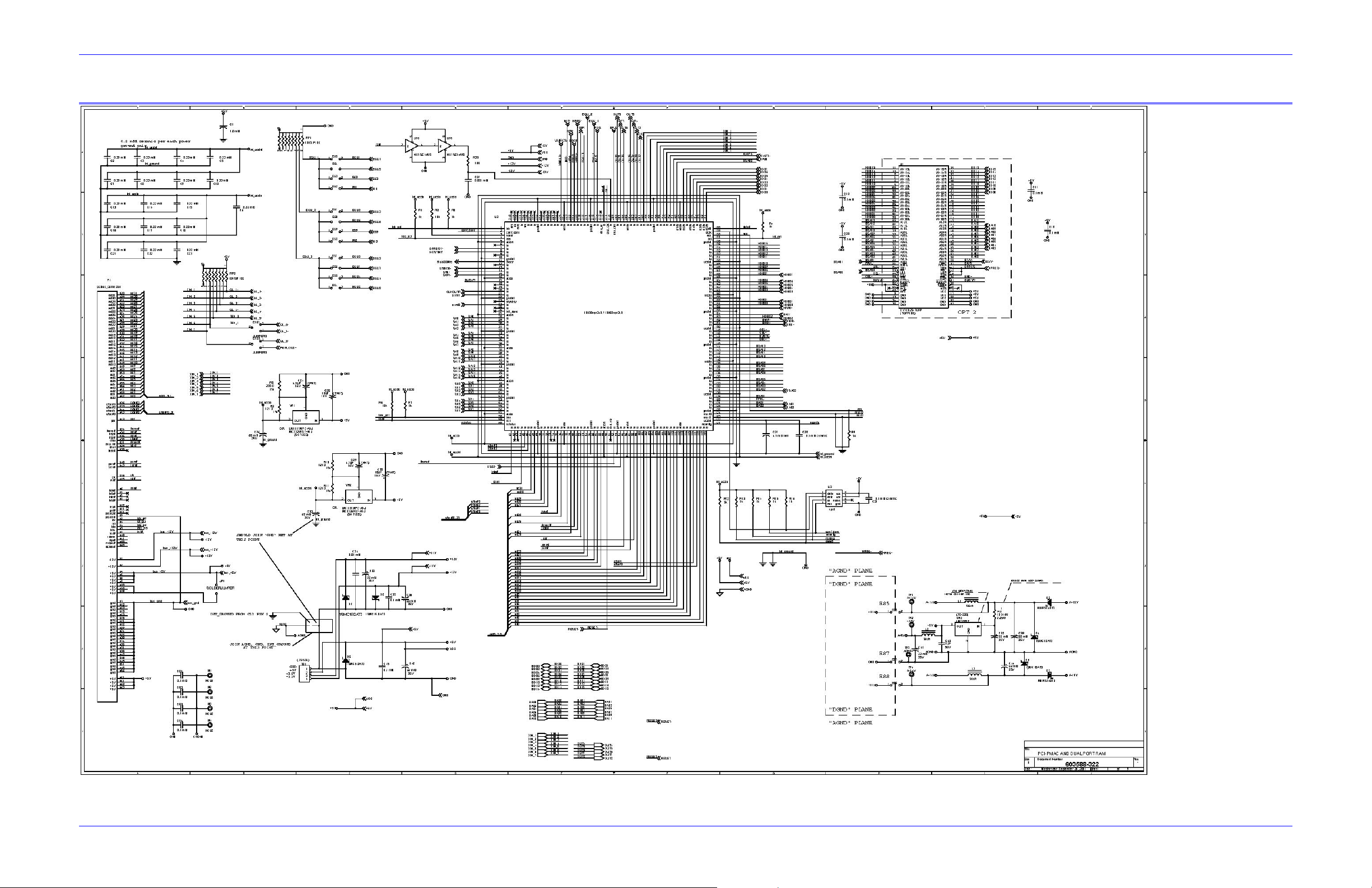
PMAC-PCI Hardware Reference
SCHEMATICS
Schematics 61
Page 72
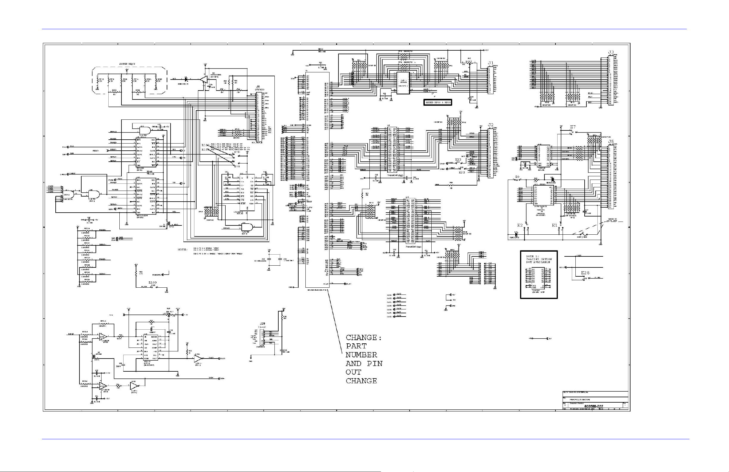
PMAC-PCI Hardware Reference
62 Schematics
Page 73
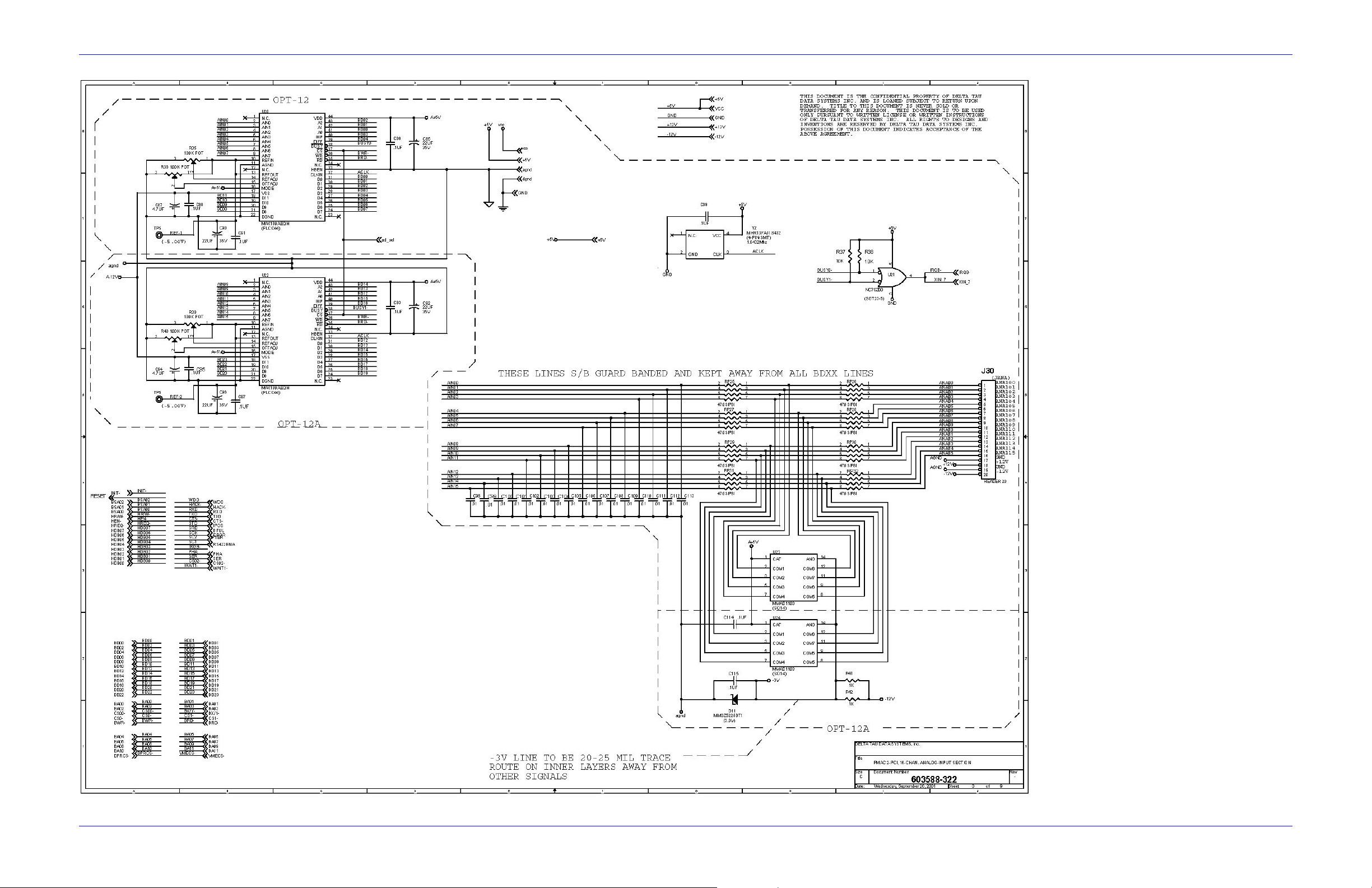
PMAC-PCI Hardware Reference
Schematics 63
Page 74

PMAC-PCI Hardware Reference
64 Schematics
Page 75

PMAC-PCI Hardware Reference
Schematics 65
Page 76

PMAC-PCI Hardware Reference
66 Schematics
Page 77

PMAC-PCI Hardware Reference
Schematics 67
Page 78

PMAC-PCI Hardware Reference
68 Schematics
Page 79

PMAC-PCI Hardware Reference
Schematics 69
 Loading...