

Page 1
^1 HARDWARE REFERENCE MANUAL
^2 PMAC2-VME
^3 Programmable Multi-Axis Controller
^4 3Ax-602413-xHxx
^5 May 27, 2004
Single Source Machine Control Power // Flexibility // Ease of Use
21314 Lassen Street Chatsworth, CA 91311 // Tel. (818) 998-2095 Fax. (818) 998-7807 // www.deltatau.com
Page 2

Copyright Information
© 2003 Delta Tau Data Systems, Inc. All rights reserved.
This document is furnished for the customers of Delta Tau Data Systems, Inc. Other uses are
unauthorized without written permission of Delta Tau Data Systems, Inc. Information contained
in this manual may be updated from time-to-time due to product improvements, etc., and may not
conform in every respect to former issues.
To report errors or inconsistencies, call or email:
Delta Tau Data Systems, Inc. Technical Support
Phone: (818) 717-5656
Fax: (818) 998-7807
Email: support@deltatau.com
Website: http://www.deltatau.com
Operating Conditions
All Delta Tau Data Systems, Inc. motion controller products, accessories, and amplifiers contain
static sensitive components that can be damaged by incorrect handling. When installing or
handling Delta Tau Data Systems, Inc. products, avoid contact with highly insulated materials.
Only qualified personnel should be allowed to handle this equipment.
In the case of industrial applications, we expect our products to be protected from hazardous or
conductive materials and/or environments that could cause harm to the controller by damaging
components or causing electrical shorts. When our products are used in an industrial
environment, install them into an industrial electrical cabinet or industrial PC to protect them
from excessive or corrosive moisture, abnormal ambient temperatures, and conductive materials.
If Delta Tau Data Systems, Inc. products are exposed to hazardous or conductive materials and/or
environments, we cannot guarantee their operation.
Page 3

PMAC2 VME Hardware Reference Manual
Table of Contents
INTRODUCTION.......................................................................................................................................................1
Features.....................................................................................................................................................................1
PMAC2 VME Configuration ....................................................................................................................................1
PMAC2 VME ASICs.............................................................................................................................................1
DSPGATE1 Servo ASIC........................................................................................................................................1
DSPGATE2 I/O ASIC...........................................................................................................................................2
PMAC2 VME Board Configuration..........................................................................................................................2
PMAC2 VME Setup ..............................................................................................................................................3
PMAC2 CPUs...........................................................................................................................................................3
Configurations......................................................................................................................................................4
Firmware..............................................................................................................................................................4
Option 16 Supplemental Memory.........................................................................................................................4
Related Technical Documentation ............................................................................................................................5
CONNECTORS...........................................................................................................................................................7
PMAC2 VME Connector Summary..........................................................................................................................7
J1/JANA (20-Pin Header).........................................................................................................................................8
J2/JTHW (26-Pin Header).........................................................................................................................................9
J3/JIO (40-Pin Header)............................................................................................................................................10
J4 (JMACRO) 26-Pin Header .................................................................................................................................11
J5/JRS232 (10-Pin Header).....................................................................................................................................11
J5A/JRS422 (26-Pin Header)..................................................................................................................................12
J6/JDISP (14-Pin Header).......................................................................................................................................13
J7/JHW (20-Pin Header).........................................................................................................................................13
J8/JEQU (10-Pin Header)........................................................................................................................................14
J9/JMACH1 (100-Pin Header)................................................................................................................................14
J10/JMACH2 (100-Pin Header)..............................................................................................................................17
P1 JMACH (96-Pin Header)...................................................................................................................................20
P2/JMACHA (96-Pin Header) ...............................................................................................................................21
TB1 (2/4-Pin Terminal Block)................................................................................................................................22
TB2 (3-Pin Terminal Block) ...................................................................................................................................22
JUMPER SUMMARY..............................................................................................................................................23
E1: Card 0 Select....................................................................................................................................................23
E2: 40 MHz/60 MHz CPU Operation................................................................................................................23
E3: Re-Initialization on Reset Control ..............................................................................................................23
E4 - E6: (Reserved for future use).....................................................................................................................23
E7A-H through E10A-H: P2 Connector B-Row Use Selec t...............................................................................24
E11-E12: JEQU Port Sink/Source Select..........................................................................................................24
E13: SCLK Direction Control...........................................................................................................................24
E17 - E18: Serial Connector Select....................................................................................................................25
E20A-I: DPRAM Byte Order Control................................................................................................................25
E39: Reset-From-Bus Enable............................................................................................................................25
Option 1V Piggyback Connector Description.........................................................................................................26
J11/JMACH3 (100-Pin Header)..............................................................................................................................26
J12/JMACH4 (100-Pin Header)..............................................................................................................................29
P2A/JMACHB (96-Pin Header)..............................................................................................................................32
OPTION 1V PIGGYBACK JUMPER SUMMARY..............................................................................................33
E14: SCLK Direction Control...........................................................................................................................33
PMAC2 VME CPU....................................................................................................................................................35
Connector Summary................................................................................................................................................35
J1 ........................................................................................................................................................................35
J2 (JEXP)............................................................................................................................................................35
Table of Contents i
Page 4

PMAC VME Hardware Reference Manual
J3 ........................................................................................................................................................................35
J4 (JEXP)............................................................................................................................................................35
J5 (JTAG/OnCE) ................................................................................................................................................35
J6 ........................................................................................................................................................................35
J7 ........................................................................................................................................................................35
PMAC2 VME CPU Board......................................................................................................................................36
PMAC2 VME CPU Piggyback Board Jumpers ......................................................................................................37
ii Table of Contents
Page 5

PMAC2 VME Hardware Reference Manual
INTRODUCTION
The PMAC2 VME provides state-of-the-art motion control for a wide variety of applications, including
machine tools, robotics, semiconductor manufacturing, packaging equipment, and general-purpose
automation. It utilizes the latest developments in electronics, software, and modern control theory to
bring motion control capabilities to a whole new level.
The PMAC2 VME is designed as a bus expansion card, but is capable of standalone operation. It is
VMEbus-compatible, with two slots and four or eight machine interface channels.
Features
PMAC2 VME supports a wide variety of servo and stepper interfaces:
• Analog +/-10V velocity command (requires Acc-8E or equivalent)
• Analog +/-10V torque command (requires Acc-8E or equivalent)
• Sinusoidal analog +/-10V phase current commands (requires Acc-8E or equivalent)
• Direct digital pulse-width modulated (PWM) phase voltage commands (requires Acc-8F, -8K or
equivalent)
• Pulse-and-direction commands (requires Acc-8S or equivalent)
• MACRO
PMAC2 VME also provides unparalleled speeds and resolutions:
• 40 MHz encoder count rate
• 18-bit analog outputs
• 18 microsecond per axis servo update time (60 MHz)
• 120 MHz PWM clock frequency (10-bit resolution at 120 kHz, 12-bit and 30 kHz, 14-bit at 7.5 kHz)
• 120 MHz MLDT (e.g. Temposonics
• 10 MHz maximum pulse-and-direction output frequency
• 10 MHz maximum position-compare output update rate
• 125 Mbit/sec optical ring network data rate
TM
ring network commands (requires Acc-42)
TM
) timer frequency (0.024mm, 0.9mil resolution)
PMAC2 VME Configuration
A PMAC2 VME board can have one or two DSPGATE1 ASICs; the first one is standard, and the second
one comes if Option 1V is ordered. It also has a DSPGATE2 ASIC supporting the non-servo I/O.
PMAC2 VME ASICs
Delta Tau has designed its own custom application-specific integrated circuits (ASICs) for the PMAC2
VME using the latest sub-micron gate-array technology. Each ASIC contains 45,000 active logic gates.
These ASICs contain all of the digital interface circuitry to tie the DSP to the machine; the rest of the
circuitry on the board is buffer circuitry.
DSPGATE1 Servo ASIC
The DSPGATE1 ASIC contains the digital servo interface circuitry for four channels, usually sufficient
for four axes of control. Each channel contains:
• Three command output sets:
• Top-and-bottom PWM or serial DAC data with clock
• Top-and-bottom PWM or serial DAC data with strobe
• Top-and-bottom PWM or PFM pulse-and-direction
• Encoder quadrature or pulse-and-direction decode and count
• Index channel input internally gated to 1 quadrature state wide
• Four flags with capability to perform hardware latching of encoder position
• HOME, PLIM, MLIM, USER
• Double-sided position-compare output with auto-increment capability
• Amplifier enable output
Introduction 1
Page 6

PMAC VME Hardware Reference Manual
• Amplifier fault input
• Four supplementary flag inputs (T, U, V, W)
• Two inputs from serial analog-to-digital converters (ADCs)
• ADC clock and strobe signal outputs
The DSPGATE1 ASIC also generates several clock frequencies necessary for hardware and software
operation, under the user’s software control:
• PWM output frequency
• DAC clock frequency
• ADC clock frequency
• Encoder sample clock frequency
• Pulse-frequency modulation (PFM) clock frequency
• Phase interrupt clock frequency
• Servo interrupt clock frequency
Note:
Phase interrupt clock frequency and Servo interrupt clock frequency are generated
from the first DSPGATE1 only.
DSPGATE2 I/O ASIC
There is also a DSPGATE2 ASIC on PMAC2 VME, which is used for interface to other I/O. The
DSPGATE2 ASIC has three parts:
• General-purpose digital I/O: 56 I/O points for JIO, JTHW, and JDISP ports
• Servo interface circuitry for 2 supplemental channels with clock generation
• MACRO ring interface circuitry
Generally, the general-purpose I/O and the servo interface circuitry on the DSPGATE2 share pins, except
for two 2-channel encoder inputs and two PWM/PFM output sub-channels. On a PMAC2 VME board,
usually the shared pins are used for general-purpose I/O instead of extra servo interface circuitry, but this
is up to the individual user.
PMAC2 VME Board Configuration
Jumpers on the PMAC2 VME determine the frequency at which the DSP on the PV CPU board will
operate. The 56002 DSP has a phased-locked loop (PLL) that allows it to multiply the crystal frequency
by a programmable integer value, permitting very high CPU frequencies with a moderate crystal
frequency. The crystal frequency on the PV CPU board is always 19.6608 MHz, commonly called 20
MHz.
The component rating of the DSP IC specifies the highest frequency at which it safely can run, but it is
the multiplication factor typically set by jumpers that specifies the frequency at which it actually runs.
Usually this is a frequency at or near the maximum for the component.
It is safe to run a DSP at a frequency below the maximum. It may be possible to run a DSP at a frequency
higher than its maximum frequency, particularly at low ambient temperatures, but safe operation cannot
be guaranteed. Unpredictable and possibly dangerous operation may result.
On power-up/reset, the DSP, operating at the crystal frequency of 20 MHz, reads the frequency jumpers
(E2 and E4) and writes into its own PLL multiplier register at X:$FFFD. Bits 0-3 of this word contain a
value one less than the multiplier value (if the frequency is being multiplied by 3, these bits contain a
value of 2).
If you wish to check the value of your multiplier, you can use the on-line command RHX:$FFFD and
look at the last hexadecimal digit. The actual multiplier is one greater than the value in this last digit.
2 Introduction
Page 7
PMAC2 VME Hardware Reference Manual
Alternately, you can define an M-variable such as M99->X:$FFFD,0,4 and then read from or write to
these bits with the M-variable.
PMAC2 VME Setup
On PMAC2 VME, jumpers E2 and E4 control the frequency of operation of the DSP according to the
following table:
E2 E4 X:$FFFD; 0-3 True Multiplier DSP Frequency
OFF OFF 1 x2 40 MHz
ON OFF 2 x3 60 MHz
OFF ON 3 x4 80 MHz
On the PMAC2 VME, I54 is read at power-up to set the baud rate clock. Because this clock is derived
from the CPU clock frequency, the proper setting of I54 is dependent on the CPU clock frequency as set
by E2 and E4. Table 1-3 shows the settings of I54 for 40, 60, and 80 MHz CPU operation.
I54 Baud Rate for 40 MHz CPU Baud Rate for 60 MHz CPU Baud Rate for 80 MHz CPU
0 600 Disabled 1200
1 900* (-0.05%) 900 1800* (-0.1%)
2 1200 1200 2400
3 1800* (-0.1%) 1800 3600* (-0.19%)
4 2400 2400 4800
5 3600* (-0.19%) 3600 7200* (-0.38%)
6 4800 4800 9600
7 7200* (-0.38%) 7200 14,400*(-0.75%)
8 9600 9600 19,200
9 14,400*(-0.75%) 14,400 28,800*(-1.5%)
10 19,200 19,200 38,400
11 28,800*(-1.5%) 28,800 57,600*(-3.0%)
12 38,400 38,400 76,800
13 57,600*(-3.0%) 57,600 115,200*(-6.0%)
14 76,800 76,800 153,600
15 Disabled 115,200 Disabled
* not an exact baud rate
PMAC2 CPUs
The PMAC2 VME CPU communicates with the axes through specially designed custom gate array ICs,
referred to as DSPGATES. Each of these ICs can handle four analog output channels, four encoders as
input, and four analog-derived inputs from accessory boards. One PMAC2 VME can utilize from one to
four of these gate array ICs, so specifying the hardware configuration amounts to counting the numbers
and types of inputs and outputs. Up to 16 PMAC2 VMEs may be ganged together with complete
synchronization, for a total of 128 axes. A PMAC2 VME may have one of three available CPU
configurations. These configurations are described in the following paragraphs.
• P/N 602398 — This is the original standard CPU board for the PMAC2 VME. It has a 20MHz clock
and a battery backup RAM.
• P/N 602405 — This is a flash memory CPU board with no battery backup. This board provides
either a 40MHz or 60MHz clock.
• P/N 602705 — The PV CPU piggyback board provides 80 MHz CPU operation and supplemental
battery-backed RAM for the PMAC2 VME.
The PV CPU board gets its name from the PV package style of the Motorola 56002 DSP IC on the board.
The board is also called the Universal CPU because it can support all speeds and configurations of the
CPU section.
Introduction 3
Page 8
PMAC VME Hardware Reference Manual
The PV CPU has operational differences from earlier CPU configurations to support the new features.
The following paragraphs explain these differences and are only relevant if using the 602705 CPU
piggyback board on the controller.
Configurations
The PV CPU board is configured at the factory to the customer’s specifications. The JEXP expansion
port is buffered, providing the capability to connect many boards on the expansion port.
The following table shows the configuration of the key components on the PV CPU board for the PMAC2
VME.
Version Main Memory
Backup
Standard Flash Empty 32-pin RAM Flash ROM Empty
Opt 5B Flash Empty 32-pin RAM Flash ROM Empty
Opt 5C Flash Empty 32-pin RAM Flash ROM Empty
+Opt 16 Flash 28-pin RAM 32-pin RAM Flash ROM Battery
U6, U9, U15
Components
U7, U10, U16
Components
U5 Components BT1 Components
Firmware
The PV CPU board does not support firmware versions previous to V1.16 of August 1996 without
changes in programming of the on-board logic (GALs). If the firmware must be changed between a
version previous to V1.16 and a version V1.16 or newer, the on-board logic must be re-programmed.
When loading new firmware into the flash configurations of the PV CPU, E4 on the CPU board must be
ON in addition to having the PMAC2 VME re-initialization jumper E3 ON.
Option 16 Supplemental Memory
If the Option 16 supplemental battery-backed parameter memory is ordered, an extra bank of memory
with battery backup circuitry is provided. This option can be ordered only if the main memory is flash
backed (Option 4A, 5A, 5B, or 5C). This memory is for user parameter storage only. From PMAC
programs it can be accessed with M-variables only (L-variables also in compiled PLCs). The on-line
direct-memory read and write commands can be used from the host computer as well.
With M-variable access, arrays can be created with indirect addressing techniques by pointing a second
M-variable to the definition of a first M-variable that points into this memory area. For example, with the
M-variable definitions:
M0->L:$A000; 1st long word of Opt. 16 RAM; floating point
M10->Y:$BC000,0,16; Low 16 bits of M0 def., with pointer address
Note:
This technique is not possible with L-variables in compiled PLCs.
The following code segment could load a sine table into the first 360 words of the Option 16 RAM:
P1=0
WHILE (P1<360)
M10=$A000+P1 ; Sets address that M0 points to
M0=SIN(P1) ; Puts value in register that M0 points to
P1=P1+1
ENDWHILE
Physically, the Option 16 memory is a 16k x 24 bank of battery-backed static RAM. It maps into the
PMAC2 VME at addresses $A000 to $BFFF, on both the X and Y data buses, an 8k x 48 block of address
space. Addresses Y:$BC00 to Y:$BFFF are double-mapped with the main flash-backed RAM for the Mvariable definitions, and should not be used for user parameter storage.
4 Introduction
Page 9

PMAC2 VME Hardware Reference Manual
Any value written into the Option 16 memory will automatically be retained through a power-down or
reset; no SAVE operation is required. The power draw on the battery is low enough that battery life will
typically be limited only by the quoted 10-year life of the battery.
Related Technical Documentation
Manual Number Manual Title
3A0-602413-363 PMAC2 User’s Manu al
3A0-602XXX-363 PMAC User’s Software Reference
Introduction 5
Page 10

PMAC VME Hardware Reference Manual
6 Introduction
Page 11
PMAC2 VME Hardware Reference Manual
CONNECTORS
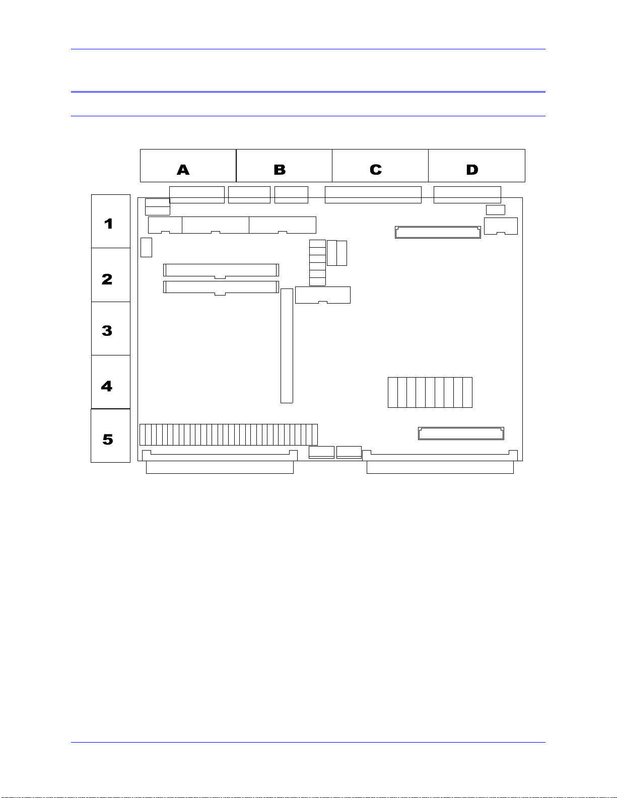
PMAC2 VME Connector Summary
The following paragraphs provide a brief description of each connector on the PMAC2 VME, its use, and
individual pinout information.
E10H
E12
E11
E13
E10G
E10F
J8
E10E
J7
J5A
J9
J10
J6
J4
J5
E1
E2
E3
E4
E6
E5
J1
J3
J14
E18
E17
J2
E39
J13
J17
E20D
E20C
E20B
E20A
E9F
E9D
E9E
E9H
E9G
E10D
E10A
E10C
E10B
E8F
E8H
E9B
E9C
E8E
E8D
E8G
E9A
E7F
E8B
E8C
E7H
E7E
E7D
E7C
E7B
E7G
E8A
E7A
E20G
J16
E20H
E20I
E20F
E20E
TB2TB1
Connectors 7
Page 12
PMAC VME Hardware Reference Manual
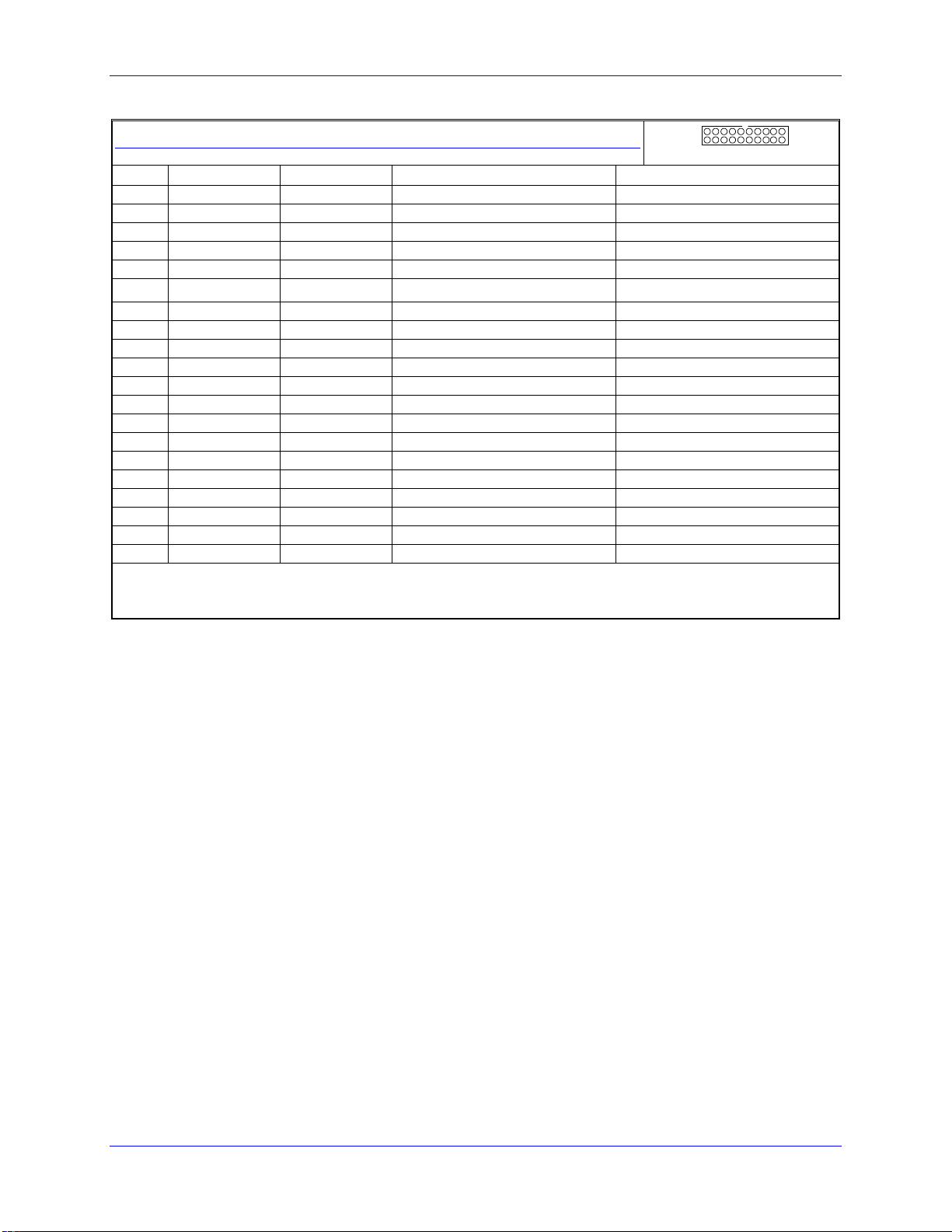
J1/JANA (20-Pin Header)
19
20
Front View
1
2
Pin # Symbol Function Description Notes
1 ANAI00 Input Analog Input 0 0-5V or +/-2.5V range
2 ANAI01 Input Analog Input 1 0-5V or +/-2.5V range
3 ANAI02 Input Analog Input 2 0-5V or +/-2.5V range
4 ANAI03 Input Analog Input 3 0-5V or +/-2.5V range
5 ANAI04 Input Analog Input 4 0-5V or +/-2.5V range
6 ANAI05 Input Analog Input 5 0-5V or +/-2.5V range
7 ANAI06 Input Analog Input 6 0-5V or +/-2.5V range
8 ANAI07 Input Analog Input 7 0-5V or +/-2.5V range
9 ANAI08 Input Analog Input 8 0-5V or +/-2.5V range (1)
10 ANAI09 Input Analog Input 9 0-5V or +/-2.5V range (1)
11 ANAI10 Input Analog Input 10 0-5V or +/-2.5V range (1)
12 ANAI11 Input Analog Input 11 0-5V or +/-2.5V range (1)
13 ANAI12 Input Analog Input 12 0-5V or +/-2.5V range (1)
14 ANAI13 Input Analog Input 13 0-5V or +/-2.5V range (1)
15 ANAI14 Input Analog Input 14 0-5V or +/-2.5V range (1)
16 ANAI15 Input Analog Input 15 0-5V or +/-2.5V range (1)
17 GND Common PMAC Common Not isolated from digital
18 +12V Output Positive Supply Voltage To power external circuitry
19 GND Common PMAC Common Not isolated from digital
20 -12V Output Negative Supply Voltage To power external circuitry
The JANA connector provides the inputs for the 8 or 16 optional analog inputs on the PMAC2.
Note: Connector J1 is present only if Option 12 is ordered. Analog inputs ANAI08 to ANAI15 are present on ly if
Option 12A is ordered in addition to Option 12.
8 Connectors
Page 13
PMAC2 VME Hardware Reference Manual
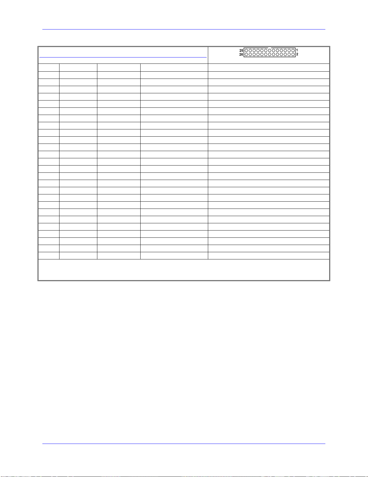
J2/JTHW (26-Pin Header)
Front View
Pin # Symbol Function Description Notes
1 GND Common PMAC Common
2 GND Common PMAC Common
3 DAT0 Input Data-0 Input Data Input from Mux Port Accessories
4 SEL0 Output Select-0 Output Address/Data Output for Mux Port Accessories
5 DAT1 Input Data-1 Input Data Input from Mux Port Accessories
6 SEL1 Output Select-1 Output Address/Data Output for Mux Port Accessories
7 DAT2 Input Data-2 Input Data Input from Mux Port Accessories
8 SEL2 Output Select-2 Output Address/Data Output for Mux Port Accessories
9 DAT3 Input Data-3 Input Data Input from Mux Port Accessories
10 SEL3 Output Select-3 Output Address/Data Output for Mux Port Accessories
11 DAT4 Input Data-4 Input Data Input from Mux Port Accessories
12 SEL4 Output Select-4 Output Address/Data Output for Mux Port Accessories
13 DAT5 Input Data-5 Input Data Input from Mux Port Accessories
14 SEL5 Output Select-5 Output Address/Data Output for Mux Port Accessories
15 DAT6 Input Data-6 Input Data Input from Mux Port Accessories
16 SEL6 Output Select-6 Output Address/Data Output for Mux Port Accessories
17 DAT7 Input Data-7 Input Data Input from Mux Port Accessories
18 SEL7 Output Select-7 Output Address/Data Output for Mux Port Accessories
19 N.C. N.C. No Connection
20 GND Common PMAC Common
21 BRLD/ Output Buffer Request Low Is Buffer Req.
22 GND Common PMAC Common
23 IPLD/ Output In Position Low Is In Position
24 GND Common PMAC Common
25 +5V Output +5Vdc Supply Power Supply Out
26 INIT/ Input PMAC Reset Low Is Reset
The JTHW connector provides eight inputs and eight outputs at TTL levels; typically these are used to create
multiplexed I/O with accessory boards such as Acc-18 (Thumbwheel) and Acc-34 (Discrete I/O). The port I/O may
also be used directly, as non-multiplexed I/O.
Connectors 9
Page 14

PMAC VME Hardware Reference Manual
40
J3/JIO (40-Pin Header)
39
Front View
1
2
Pin # Symbol Function Description Notes
1 I/O00 In/Out Digital I/O 0 Software direction ctrl.
2 I/O01 In/Out Digital I/O 1 Software direction ctrl.
3 I/O02 In/Out Digital I/O 2 Software direction ctrl.
4 I/O03 In/Out Digital I/O 3 Software direction ctrl.
5 I/O04 In/Out Digital I/O 4 Software direction ctrl.
6 I/O05 In/Out Digital I/O 5 Software direction ctrl.
7 I/O06 In/Out Digital I/O 6 Software direction ctrl.
8 I/O07 In/Out Digital I/O 7 Software direction ctrl.
9 I/O08 In/Out Digital I/O 8 Software direction ctrl.
10 I/O09 In/Out Digital I/O 9 Software direction ctrl.
11 I/O10 In/Out Digital I/O 10 Software direction ctrl.
12 I/O11 In/Out Digital I/O 11 Software direction ctrl.
13 I/O12 In/Out Digital I/O 12 Software direction ctrl.
14 I/O13 In/Out Digital I/O 13 Software direction ctrl.
15 I/O14 In/Out Digital I/O 14 Software direction ctrl.
16 I/O15 In/Out Digital I/O 15 Software direction ctrl.
17 I/O16 In/Out Digital I/O 16 Software direction ctrl.
18 I/O17 In/Out Digital I/O 17 Software direction ctrl.
19 I/O18 In/Out Digital I/O 18 Software direction ctrl.
20 I/O19 In/Out Digital I/O 19 Software direction ctrl.
21 I/O20 In/Out Digital I/O 20 Software direction ctrl.
22 I/O21 In/Out Digital I/O 21 Software direction ctrl.
23 I/O22 In/Out Digital I/O 22 Software direction ctrl.
24 I/O23 In/Out Digital I/O 23 Software direction ctrl.
25 I/O24 In/Out Digital I/O 24 Software direction ctrl.
26 I/O25 In/Out Digital I/O 25 Software direction ctrl.
27 I/O26 In/Out Digital I/O 26 Software direction ctrl.
28 I/O27 In/Out Digital I/O 27 Software direction ctrl.
29 I/O28 In/Out Digital I/O 28 Software direction ctrl.
30 I/O29 In/Out Digital I/O 29 Software direction ctrl.
31 I/O30 In/Out Digital I/O 30 Software direction ctrl.
32 I/O31 In/Out Digital I/O 31 Software direction ctrl.
33 GND Common Reference Voltage
34 GND Common Reference Voltage
35 PHASE/ Output Phase Clock For latching data
36 SERVO/ Output Servo Clock For latching data
37 GND Common Reference Voltage
38 GND Common Reference Voltage
39 +5V Output Supply Voltage To power external circuitry
40 +5V Output Supply Voltage To power external circuitry
The JI/O connector provides 32 input/output pins at TTL levels. Direction can be controlled in byte-wide groups.
10 Connectors
Page 15

PMAC2 VME Hardware Reference Manual
J4 (JMACRO) 26-Pin Header
Front View
Pin # Symbol Function Description Notes
1 DOUT7 Output Ring Out Bit 7 Macro Ring Command
2 DOUT6 Output Ring Out Bit 6 Macro Ring Transmit
3 DOUT5 Output Ring Out Bit 5 Macro Ring Transmit
4 DOUT4 Output Ring Out Bit 4 Macro Ring Transmit
5 DOUT3 Output Ring Out Bit 3 Macro Ring Transmit
6 DOUT2 Output Ring Out Bit 2 Macro Ring Transmit
7 DOUT1 Output Ring Out Bit 1 Macro Ring Transmit
8 DOUT0 Output Ring Out Bit 0 Macro Ring Transmit
9 CMD_IN Input
10 DIN7 Input Ring In Bit 7 Macro Ring Receive
11 DIN6 Input Ring In Bit 6 Macro Ring Receive
12 DIN5 Input Ring In Bit 5 Macro Ring Receive
13 DIN4 Input Ring In Bit 4 Macro Ring Receive
14 DIN3 Input Ring In Bit 3 Macro Ring Receive
15 DIN2 Input Ring In Bit 2 Macro Ring Receive
16 DIN1 Input Ring In Bit 1 Macro Ring Receive
17 DIN0 Input Ring In Bit 0 Macro Ring Receive
18 CMD_OUT Output
19 TCLK Output Ring Clock 10 MHz
20 GND Common Reference Voltage
21 STB_OUT Output Byte Strobe
22 GND Common Reference Voltage
23 DAT_STB Input Data Byte Strobe
24 GND Common Reference Voltage
25 CMD_STB Input Cmd Byte Strobe
26 VLTN Input Violation Flag Taxi Chip Receive Error
The JMACRO Network Ring Interface Connector provides the interface to the Acc-42 MACRO driver/receiver
accessory board.
J5/JRS232 (10-Pin Header)
Front View
Pin # Symbol Function Description Notes
1 PHASE In/Out Phasing Clock See Notes 1, 2
2 DTR Bidirect Data Term Rdy Tied to DSR
3 TXD/ Input Receive Data Host transmit data
4 CTS Input Clear To Send Host ready bit
5 RXD/ Output Send Data Host receive data
6 RTS Output Req. To Send PMAC ready bit
7 DSR Bidirect Data Set Ready Tied to DTR
8 SERVO In/Out Servo Clock See Note 2
9 GND Common Pmac Common
10 +5V Output +5vdc Supply Power Supply Out
This connector is used for serial communications on a PMAC2 VME if E17 and E18 jumpers connect pins 1 and
2. This connector cannot be used for daisy chain communication interconnection of multiple PMACs, although it
can be used to share servo and phase clocks for synchronicity. TheJ5A RS-422 interface is required for daisy
chain communication.
Note 1: If communicating to PMAC2 over this connector with a modem style terminal emulator such as
Microsoft Windows Terminal, line 1 should not be co nnected.
Note 2: SERVO and PHASE are outputs if jumper E1 is OFF; they are inputs if jumper E1 is ON.
Connectors 11
Page 16

PMAC VME Hardware Reference Manual
J5A/JRS422 (26-Pin Header)
Front View
Pin # Symbol Function Description Notes
1 CHASSI Common PMAC Common
2 S+5V Output +5Vdc Supply
3 RD- Input Receive Data Diff. I/O Low True **
4 RD+ Input Receive Data Diff. I/O High True *
5 SD- Output Send Data Diff. I/O Low True **
6 SD+ Output Send Data Diff. I/O High True *
7 CS+ Input Clear to Send Diff. I/O High True **
8 CS- Input Clear to Send Diff. I/O Low True *
9 RS+ Output Req. to Send Diff. I/O High True **
10 RS- Output Req. to Send Diff. I/O Low True *
11 DTR Bidirect Data Term Read Tied to DSR
12 INIT/ Input PMAC Reset Low is Reset
13 GND Common PMAC Common **
14 DSR Bidirect Data Set Ready Tied to DTR
15 SDIO- Bidirect Special Data Diff. I/O Low True
16 SDIO+ Bidirect Special Data Diff. I/O High True
17 SCIO- Bidirect Special Ctrl. Diff. I/O Low True
18 SCIO+ Bidirect Special Ctrl. Diff. I/O High True
19 SCK- Bidirect Special Clock Diff. I/O Low True
20 SCK+ Bidirect Special Clock Diff. I/O High True
21 SERVO- Bidirect Servo Clock Diff. I/O Low True ***
22 SERVO+ Bi di rect Servo Clock Diff. I/O High True ***
23 PHASE- Bidirect Phase Clock Diff. I/O Low True ***
24 PHASE+ Bidirect Phase Clock Diff. I/O High True ***
25 GND Common PMAC Common
26 +5V Output +5vdc Supply Power supply out
This connector can be used for serial communications on a PMAC2 VME if E17 and E18 jumpers connect pins 2
and 3. If these jumpers connect pins 1 and 2, the J5 RS-232 connector should be used instead for serial
communications. In addition, this connector is used to daisy chain interconnect multiple PMACs for synchronized
operation.
Note: Jumpers E17 and E18 must connect pins 2 and 3 to use this port for serial communications.
12 Connectors
Page 17

PMAC2 VME Hardware Reference Manual
J6/JDISP (14-Pin Header)
Front View
Pin # Symbol Function Description Notes
1 VDD Output +5V Power Power Supply Out
2 VSS Common PMAC Common
3 RS Output Read Strobe TTL Signal Out
4 VEE Output Contrast Adjust VEE 0 to +5Vdc *
5 E Output Display Enable High is Enable
6 R/W Output Read Or Write TTL Signal Out
7 DB1 Output Display Data1
8 DB0 Output Display Data0
9 DB3 Output Display Data3
10 DB2 Output Display Data2
11 DB5 Output Display Data5
12 DB4 Output Display Data4
13 DB7 Output Display Data7
14 DB6 Output Display Data6
The JDISP connector is used to drive the 2-line x 24-charact er (acc -12), 2 x 40 (acc-12a) LCD, or the 2 x 40
vacuum fluorescent (acc 12c) display unit. The display command may be used to send messages and values to the
display.
J7/JHW (20-Pin Header)
19
20
Front View
1
2
Pin # Symbol Function Description Notes
1 GND Common Ref. Voltage
2 +5V Output Supply Voltage To power external circuitry
3 HWA1+ Input Hw Pos A Chan. Also pulse input
4 HWA1- Input Hw Neg A Chan. Also pulse input
5 HWB1+ Input Hw Pos B Chan. Also direction input
6 HWB1- Input Hw Neg B Chan. Also direction input
7 HWA2+ Input Hw Pos A Chan. Also pulse input
8 HWA2- Input Hw Neg A Chan. Also pulse input
9 HWB2+ Input Hw Pos B Chan. Also direction input
10 HWB2- Input Hw Neg B Chan. Also direction input
11 PUL1+ Output Pfm Pos Pulse Also PWM output
12 PUL1- Output Pfm Neg Pulse Also PWM output
13 DIR1+ Output Pfm Pos Dir. Out Also PWM output
14 DIR1- Output Pfm Neg Dir Out Also PWM output
15 PUL2+ Output Pfm Pos Pulse Also PWM output
16 PUL2- Output Pfm Neg Pulse Also PWM output
17 DIR2+ Output Pfm Pos Dir. Out Also PWM output
18 DIR2- Output Pfm Neg Dir Out Also PWM output
19 GND Common Ref. Voltage
20 +5V Output Supply Voltage To power external circuitry
Typically, this connector provides the interface for two quadrature encoders to be used as handwheel or time-base
master encoders.
Connectors 13
Page 18

PMAC VME Hardware Reference Manual
2
99
J8/JEQU (10-Pin Header)
Front View
Pin # Symbol Function Description Notes
1 EQU1/ Output Enc. 1 Comp-Eq Low is true
2 EQU2/ Output Enc. 2 Comp-Eq Low is true
3 EQU3/ Output Enc. 3 Comp-Eq Low is true
4 EQU4/ Output Enc. 4 Comp-Eq Low is true
5 EQU5/ Output Enc. 5 Comp-Eq Low is true
6 EQU6/ Output Enc. 6 Comp-Eq Low is true
7 EQU7/ Output Enc. 7 Comp-Eq Low is true
8 EQU8/ Output Enc. 8 Comp-Eq Low is true
9 +V Supply Positive Supply +5V to +24V
10 GND Common Digital Ground
This connector provides the position-compare outputs for the eight encoder channels.
J9/JMACH1 (100-Pin Header)
00
Front View
Pin# Symbol Function Description Notes
1 +5V Output / Input +5V Power For external circuit or from external
supply
2 +5V Output / Input +5V Power
3 GND Common Reference Voltage
4 GND Common Reference Voltage
5 CHA1+ Input Enc 1 Pos. A Chan. Also pulse input
6 CHA1- Input Enc 1 Neg. A Chan.
7 CHB1+ Input Enc 1 Pos. B Chan. Also direction input
8 CHB1- Input Enc 1 Neg. B Chan.
9 CHC1+ Input Enc 1 Pos. C Chan. Index channel
10 CHC1- Input Enc 1 Neg. C Chan.
11 CHU1 Input Chan 1 U Flag Ha ll effect, fault code, or sub-count
12 CHV1 Input Chan 1 V Flag Ha ll effect, fault code, or sub-count
13 CHW1 Input Chan 1 W Flag Hall effect, fault code, or sub-count
14 CHT1 Input Chan 1 T Flag Fault code, or sub-count
15 USER1 Input General Purpose User Flag Hardware capture flag, or sub-count
16 PLIM1 Input Positive Overtravel Limit Hardware capture flag
17 MLIM1 Input Negative Overtravel Limit Hardware capture flag
18 HOME1 Input Home Switch Input Hardware capture flag
19 ACCFLT1 Input Accessory Fault Flag For loss of ACC supply voltage
20 WD0/ Output Watchdog Output Low is PMAC watchdog fault
21 SCLK12+ Input/Output Encoder Sample Clock Direction controlled by PMAC2
jumper
22 SCLK12- Input/Output Encoder Sample Clock
23 ADC_CLK1+ Output A/D Converter Clock Programmable frequency
24 ADC_CLK1- Output A/D Converter Clock
25 ADC_STB1+ Output A/D Converter Strobe Programmable sequence
26 ADC_STB1- Output A/D Converter Strobe
27 ADC_DAA1+ Input Chan A Adc Serial Data MSB first
28 ADC_DAA1- Input Chan A Adc Serial Data
29 ADC_DAB1+ Input Chan B Adc Serial Data MSB first
30 ADC_DAB1- Input Chan B Adc Serial Data
31 AENA1+ Output Amplifier Enable High is enable
32 AENA1- Output Amplifier Enable Low is enable
1
14 Connectors
Page 19

PMAC2 VME Hardware Reference Manual
2
99
J9/JMACH1 (100-Pin Header)
00
Front View
Pin# Symbol Function Description Notes
33 FAULT1+ Input Amplifier Fault Programmable polarity
34 FAULT1- Input Amplifier Fault
35 PWMATOP1+
DAC_CLK1+
36 PWMATOP1-
DAC_CLK1-
37 PWMABOT1+
DAC1A+
38 PWMABOT1-
DAC1A-
39 PWMBTOP1+
DAC_STB1+
40 PWMBTOP1-
DAC_STB1-
41 PWMBBOT1+
DAC1B+
42 PWMBBOT1-
DAC1B-
43 PWMCTOP1+
DIR1+
44 PWMCTOP1-
DIR1-
45 PWMCBOT1+
PULSE1+
46 PWMCBOT1-
PULSE147 GND Common Reference Voltage
48 GND Common Reference Voltage
49 +5V Output / Input +5V Power For external circuit or from external
50 +5V Output / Input +5V Power
51 +5V Output / Input +5V Power For external circuit or from external
52 +5V Output / Input +5V Power
53 GND Common Reference Voltage
54 GND Common Reference Voltage
55 CHA2+ Input Enc 2 Pos. A Chan. Also pulse input
56 CHA2- Input Enc 2 Neg. A Chan.
57 CHB2+ Input Enc 2 Pos. B Chan. Also direction input
58 CHB2- Input Enc 2 Neg. B Chan.
59 CHC2+ Input Enc 2 Pos. C Chan. Index channel
60 CHC2- Input Enc 2 Neg. C Chan.
61 CHU2 Input Chan 2 U Flag Ha ll effect, fault code, or sub-count
62 CHV2 Input Chan 2 V Flag Ha ll effect, fault code, or sub-count
63 CHW2 Input Chan 2 W Flag Hall effect, fault code, or sub-count
64 CHT2 Input Chan 2 T Flag Fault code, or sub-count
65 USER2 Input General Purpose User Flag Hardware capture flag, or sub-count
66 PLIM2 Input Positive Overtravel Limit Hardware capture flag
67 MLIM2 Input Negative Overtravel Limit Hardware capture flag
68 HOME2 Input Home Switch Input Hardware capture flag
Output Phase A Top CMD or DAC
Clock
Output Phase A Top CMD or DAC
Clock
Output Phase A Bottom CMD or DAC A
Serial Data
Output Phase A Bottom CMD or DAC A
Serial Data
Output Phase B Top CMD or DAC
Strobe
Output Phase B Top CMD or DAC
Strobe
Output Phase B Bottom CMD or DAC B
Serial Data
Output Phase B Bottom CMD or DAC B
Serial Data
Output Phase B Top CMD or PFM
Direction
Output Phase B Top CMD or PFM
Direction
Output Phase B Bottom CMD or PFM
Pulse
Output Phase B Bottom CMD or PFM
Pulse
Programmable function control
Programmable function control
Programmable function control
Programmable function control
Programmable function control
Programmable function control
supply
supply
1
Connectors 15
Page 20

PMAC VME Hardware Reference Manual
2
99
J9/JMACH1 (100-Pin Header)
00
Front View
Pin# Symbol Function Description Notes
69 ACCFLT2 Input Accessory Fault Flag For loss of ACC supply voltage
70 WD0/ Output Watchdog Output Low is PMAC watchdog fault
71 SCLK12+ Input / Output Encoder Sample Clock Direction controlled by PMAC2
jumper
72 SCLK12- Input / Output Encoder Sample Clock
73 ADC_CLK2+ Output A/D Converter Clock Programmable Frequency
74 ADC_CLK2- Output A/D Converter Clock
75 ADC_STB2+ Output A/D Converter Strobe Programmable sequence
76 ADC_STB2- Output A/D Converter Strobe
77 ADC_DAA2+ Input Chan A Adc Serial Data MSB First
78 ADC_DAA2- Input Chan A Adc Serial Data
79 ADC_DAB2+ Input Chan B Adc Serial Data MSB First
80 ADC_DAB2- Input Chan B Adc Serial Data
81 AENA2+ Output Amplifier Enable High Is Enable
82 AENA2- Output Amplifier Enable Low Is Enable
83 FAULT2+ Input Amplifier Fault Programmable polarity
84 FAULT2- Input Amplifier Fault
85 PWMATOP2+
DAC_CLK2+
86 PWMATOP2-
DAC_CLK2-
87 PWMABOT2+
DAC2A+
88 PWMABOT2-
DAC2A-
89 PWMBTOP2+
DAC_STB2+
90 PWMBTOP2-
DAC_STB2-
91 PWMBBOT2+
DAC2B+
92 PWMBBOT2-
DAC2B-
93 PWMCTOP2+
DIR2+
94 PWMCTOP2-
DIR2-
95 PWMCBOT2+
PULSE2+
96 PWMCBOT2-
PULSE2-
Output Phase A Top CMD or DAC
Clock
Output Phase A Top CMD or DAC
Clock
Output Phase A Bottom CMD or DAC A
Serial Data
Output Phase A Bottom CMD or DAC A
Serial Data
Output Phase B Top CMD or DAC
Strobe
Output Phase B Top CMD or DAC
Strobe
Output Phase B Bottom CMD or DAC B
Serial Data
Output Phase B Bottom CMD or DAC B
Serial Data
Output Phase B Top CMD or PFM
Direction
Output Phase B Top CMD or PFM
Direction
Output Phase B Bottom CMD or PFM
Pulse
Output Phase B Bottom CMD or PFM
Pulse
Programmable function control
Programmable function control
Programmable function control
Programmable function control
Programmable function control
Programmable function control
97 GND Common Reference Voltage
98 GND Common Reference Voltage
99 +5V Output / Input +5V Power For external circuit or from external
supply
100 +5V Output / Input +5V Power
The JMACH1 connector provides the interface pins for channels 1 and 2. Usually, it is connected to a breakout board,
such as one of the Acc-8x family of boards or an application-specific interface board.
Note: 100-pin male box header with center key, 0050 pitch. AMP part # 1-04068-7. Delta Tau part # 014-00010-FPB.
1
16 Connectors
Page 21

PMAC2 VME Hardware Reference Manual
2
99
J10/JMACH2 (100-Pin Header)
00
Front View
1
Pin# Symbol Function Description Notes
1 +5V Output / Input +5V Power For external circuit or from ext.
Supply
2 +5V Output / Input +5V Power
3 GND Common Reference Voltage
4 GND Common Reference Voltage
5 CHA3+ Input Enc 3 Pos. A Chan. Also pulse input
6 CHA3- Input Enc 3 Neg. A Chan.
7 CHB3+ Input Enc 3 Pos. B Chan. Also direction input
8 CHB3- Input Enc 3 Neg. B Chan.
9 CHC3+ Input Enc 3 Pos. C Chan. Index channel
10 CHC3- Input Enc 3 Neg. C Chan.
11 CHU3 Input Chan 3 U Flag Ha ll effect, fault code, or sub-
count
12 CHV3 Input Chan 3 V Flag Ha ll effect, fault code, or sub-
count
13 CHW3 Input Chan 3 W Flag Hall effect, fault code, or sub-
count
14 CHT3 Input Chan 3 T Flag Fault code, or sub-count
15 USER3 Input General Purpose
User Flag
16 PLIM3 Input Positive Overtravel Limit Hardware capture flag
17 MLIM3 Input Negative Overtravel Limit Hardware capture flag
18 HOME3 Input Home Switch Input Hardware capture flag
19 ACCFLT3 Input Accessory Fault Flag For loss of ACC supply voltage
20 WD0/ Output Watchdog Output Low is PMAC watchdog fault
21 SCLK34+ Input / Output Encoder Sample Clock Direction controlled by PMAC2
22 SCLK34- Input / Output Encoder Sample Clock
23 ADC_CLK3+ Output A/D Converter Clock Programmable frequency
24 ADC_CLK3- Output A/D Converter Clock
25 ADC_STB3+ Output A/D Converter Strobe Programmable sequence
26 ADC_STB3- Output A/D Converter Strobe
27 ADC_DAA3+ Input Chan A Adc Serial Data MSB first
28 ADC_DAA3- Input Chan A Adc Serial Data
29 ADC_DAB3+ Input Chan B Adc Serial Data MSB first
30 ADC_DAB3- Input Chan B Adc Serial Data
31 AENA3+ Output Amplifier Enable High is enable
32 AENA3- Output Amplifier Enable Low is enable
33 FAULT3+ Input Amplifier Fault Programmable polarity
34 FAULT3- Input Amplifier Fault
35 PWMATOP3+
DAC_CLK3+
36 PWMATOP3-
DAC_CLK3-
37 PWMABOT3+
DAC3A+
38 PWMABOT3-
DAC3A-
39 PWMBTOP3+
DAC_STB3+
Output Phase A Top CMD or DAC
Clock
Output Phase A Top CMD or DAC
Clock
Output Phase A Bottom CMD or DAC A
Serial Data
Output Phase A Bottom CMD or DAC A
Serial Data
Output Phase B Top CMD or DAC
Strobe
Hardware capture flag, or subcount
jumper
Programmable Function Control
Programmable function control
Programmable function control
Connectors 17
Page 22

PMAC VME Hardware Reference Manual
2
99
J10/JMACH2 (100-Pin Header)
00
Front View
Pin# Symbol Function Description Notes
40 PWMBTOP3-
DAC_STB3-
41 PWMBBOT3+
DAC3B+
42 PWMBBOT3-
DAC3B-
43 PWMCTOP3+
DIR3+
44 PWMCTOP3-
DIR3-
45 PWMCBOT3+
PULSE3+
46 PWMCBOT3-
PULSE347 GND Common Reference Voltage
48 GND Common Reference Voltage
49 +5V Output / Input +5V Power For external circuit or from
50 +5V Output / Input +5V Power
51 +5V Output / Input +5V Power For external circuit or from
52 +5V Output / Input +5V Power
53 GND Common Reference Voltage
54 GND Common Reference Voltage
55 CHA4+ Input Enc 4 Pos. A Chan. Also pulse input
56 CHA4- Input Enc 4 Neg. A Chan.
57 CHB4+ Input Enc 4 Pos. B Chan. Also direction input
58 CHB4- Input Enc 4 Neg. B Chan.
59 CHC4+ Input Enc 4 Pos. C Chan. Index channel
60 CHC4- Input Enc 4 Neg. C Chan.
61 CHU4 Input Chan 4 U Flag Ha ll effect, fault code, or sub-
62 CHV4 Input Chan 4 V Flag Ha ll effect, fault code, or sub-
63 CHW4 Input Chan 4 W Flag Hall effect, fault code, or sub-
64 CHT4 Input Chan 4 T Flag Fault code, or sub-count
65 USER4 Input General Purpose User Flag Hardware capture flag, or sub-
66 PLIM4 Input Positive Overtravel Limit Hardware capture flag
67 MLIM4 Input Negative Overtravel Limit Hardware capture flag
68 HOME4 Input Home Switch Input Hardware capture flag
69 ACCFLT4 Input Accessory Fault Flag For loss of ACC supply voltage
70 WD0/ Output Watchdog Output Low is PMAC watchdog fault
71 SCLK34+ Input / Output Encoder Sample Clock Direction controlled by PMAC2
72 SCLK34- Input / Output Encoder Sample Clock
73 ADC_CLK4+ Output A/D Converter Clock Programmable frequency
74 ADC_CLK4- Output A/D Converter Clock
75 ADC_STB4+ Output A/D Converter Strobe Programmable sequence
Output Phase B Top CMD or DAC
Strobe
Output Phase B Bottom CMD or DAC B
Serial Data
Output Phase B Bottom CMD or DAC B
Serial Data
Output Phase B Top CMD or PFM
Direction
Output Phase B Top CMD or PFM
Direction
Output Phase B Bottom CMD or PFM
Pulse
Output Phase B Bottom CMD or PFM
Pulse
Programmable function control
Programmable function control
Programmable function control
external supply
external supply
count
count
count
count
jumper
1
18 Connectors
Page 23

PMAC2 VME Hardware Reference Manual
2
99
J10/JMACH2 (100-Pin Header)
00
Front View
1
Pin# Symbol Function Description Notes
76 ADC_STB4- Output A/D Converter Strobe
77 ADC_DAA4+ Input Chan A Adc Serial Data MSB first
78 ADC_DAA4- Input Chan A Adc Serial Data
79 ADC_DAB4+ Input Chan B Adc Serial Data MSB first
80 ADC_DAB4- Input Chan B Adc Serial Data
81 AENA4+ Output Amplifier Enable High is enable
82 AENA4- Output Amplifier Enable Low is enable
83 FAULT4+ Input Amplifier Fault Programmable polarity
84 FAULT4- Input Amplifier Fault
85 PWMATOP4+
DAC_CLK4+
86 PWMATOP4-
DAC_CLK4-
87 PWMABOT4+
DAC4A+
88 PWMABOT4-
DAC4A-
89 PWMBTOP4+
DAC_STB4+
90 PWMBTOP4-
DAC_STB4-
91 PWMBBOT4+
DAC4B+
92 PWMBBOT4-
DAC4B-
93 PWMCTOP4+
DIR4+
94 PWMCTOP4-
DIR4-
95 PWMCBOT4+
PULSE4+
96 PWMCBOT4-
PULSE4-
Output Phase A Top CMD or DAC
Clock
Output Phase A Top CMD or DAC
Clock
Output Phase A Bottom CMD or DAC A
Serial Data
Output Phase A Bottom CMD or DAC A
Serial Data
Output Phase B Top CMD or DAC
Strobe
Output Phase B Top CMD or DAC
Strobe
Output Phase B Bottom CMD or DAC B
Serial Data
Output Phase B Bottom CMD or DAC B
Serial Data
Output Phase B Top CMD or PFM
Direction
Output Phase B Top CMD or PFM
Direction
Output Phase B Bottom CMD or PFM
Pulse
Output Phase B Bottom CMD or PFM
Pulse
Programmable function control
Programmable function control
Programmable function control
Programmable function control
Programmable function control
Programmable function control
97 GND Common Reference Voltage
98 GND Common Reference Voltage
99 +5V Output / Input +5V Power For external circuit or from
external supply
100 +5V Output / Input +5V Power
The JMACH2 connector provides the interface pins for channels 3 and 4. Usually, it is connected to a breakout
board, such as one of the Acc-8x family of boards, or an application-specific interface board.
Note: 100-pin male box header with center key, 0050 pitch. AMP part # 1-04068-7. Delta Tau part # 014-00010FPB.
Connectors 19
Page 24

PMAC VME Hardware Reference Manual
P1 JMACH (96-Pin Header)
Front View
Pin # Row A Row B Row C
01 D00 BBSY/ D08
02 D01 BCLR/ D09
03 D02 ACFAIL/ D10
04 D03 B0IN/ D11
05 D04 BG0OUT/ D12
06 D05 BG1IN/ D13
07 D06 BG1OUT/ D14
08 D07 BG2IN/ D15
09 GND BG2OUT/ GND
10 SYSCLK BG3IN/ SYSFAIL/
11 GND BG3OUT/ BERR/
12 DS1/ BR0/ SYSRESET/
13 DS0/ BR1/ LWORD/
14 WRITE/ BR2/ AM5
15 GND BR3/ A23
16 DTACK/ AM0 A22
17 GND AM1 A21
18 AS/ AM2 A20
19 GND AM3 A19
20 IACK/ GND A18
21 IACKIN/ SERCLK A17
22 IACKOUT/ SERDAT/ A16
23 AM4 GND A15
24 A07 IRQ7/ A14
25 A06 IRQ6/ A13
26 A05 IRQ5/ A12
27 A04 IRQ4/ A11
28 A03 IRQ3/ A10
29 A02 IRQ2/ A09
30 A01 IRQ1/ A08
31 -12V +5V STDBY +12V
32 +5V +5V +5V
This is the standard VME connector. It is sufficient for 16-bit or 24-bit addressing and for 8-bit or 16-bit data.
For 32-bit addressing the b-row of P2 must be used as well. PMAC does not support 32-bit data transfers over the
bus, even with the b-row of P2. If P1 is connected to the VME backplane, PMAC is connected to the +5V supply
and GND automatically. In this case, no other +5V supply should be connected.
20 Connectors
Page 25

PMAC2 VME Hardware Reference Manual
P2/JMACHA (96-Pin Header)
Front View
Pin# Row A Row B (Format A) Row B (Format B) Row C
01 +5V +5V CHU1 +5V
02 GND GND CHU3 GND
03 CHA1 (Reserved) CHV1 CHA3
04 CHB1 VA24 CHV3 CHB3
05 CHC1 VA25 CHW1 CHC3
06 PLIM1 VA26 CHW3 PLIM3
07 MLIM1 VA27 CHT1 MLIM3
08 HOME1 VA28 CHT3 HOME3
09 AENA1 VA29 USER1 AENA3
10 FAULT1 VA30 USER3 FAULT3
11 PWMATOP1/
DAC_CLK1
VA31 ADC_DAA1 PWMATOP3/
DAC_CLK3
12 PWMABOT1/ DAC1A GND ADC_DAA3 PWMABOT3/ DAC3A
13 PWMBTOP1/
DAC_STB1
+5V ADC_DAB1 PWMBTOP3/
DAC_STB3
14 PWMBBOT1/ DAC1B VD1 6 (n ot used) ADC_DAB3 PWMBBOT3/ DAC3B
15 PWMCTOP1/ DIR1 VD17 (not used) ADC_CLK 1234 PWMCTOP3/ DIR3
16 PWMCBOT1/ PULSE1 VD18 (not used) ADC_STB1234 PWMCBOT 3/ PULSE3
17 CHA2 VD19 (not used) SCLK1234 CHA4
18 CHB2 VD20 (not used) WD0/ CHB4
19 CHC2 VD21 (not used) CHU2 CHC4
20 PLIM2 VD22 (not used) CHU4 PLIM4
21 MLIM2 VD23 (not used) CHV2 MLIM4
22 HOME2 GND CHV4 HOME4
23 AENA2 VD24 (not used) CHW2 AENA4
24 FAULT2 VD25 (not used) CHW4 FAULT4
25 PWMATOP2/
DAC_CLK2
VD26 (not used) CHT2 PWMATOP4/
DAC_CLK4
26 PWMABOT2/ DAC2A VD27 (not used) CHT4 PWMABOT4/ DAC4A
27 PWMBTOP2/
DAC_STB2
VD28 (not used) USER2 PWMBTOP4/
DAC_STB4
28 PWMBBOT2/ DAC2B VD29 (n ot used) USER4 PWMBBOT4/ DAC4B
29 PWMCTOP2/ DIR2 VD30 (not used) ADC_DAA2 PWMCTOP4/ DIR4
30 PWMCBOT2/ PULSE2 VD31 (not used) ADC_DAA4 PWMCBOT4/ PULSE4
31 GND GND ADC_DAB2 GND
32 +5V +5V ADC_DAB4 +5V
The P2 connector provides an alternate path to J9 and J10 for the machine interface connections for channels 1-4.
Only the positive signals of complementary pairs are brought out on this connector. For the inpu ts, the
complementary lines are tied to 2.5V on PMAC2. Refer to the J9 and J10 pin descriptions for more detailed
information on each pin.
Note: Format A for the B-row will be used if E7A-H, E8A-H, E9A-H, and E10A-H connect pins 2 and 3. This
format must be used for a 32-bit VME system. Format B for the B-row will be used if these jumpers connect pins
1 and 2. This format is not compatible with 32-bit VME systems.
Connectors 21
Page 26

PMAC VME Hardware Reference Manual
TB1 (2/4-Pin Terminal Block)
Pin# Symbol Function Description Notes
1 GND Common Reference Voltage
2 +5V Input Positive Supply Voltage Supplies all PMAC digital circuits
3 +12V Input Positive Supply Voltage +12v to +15v; not required on-board;
used on j1 to supply analog inputs
4 -12V Input Negative Supply Voltage -12V to –15V; required for Opt-12
ADCs; used on J1 to supply analog
inputs
This terminal block can be used to provide the input for the power supply for the circuits on the PMAC2 board
when it is not in a bus configuration. When the PMAC2 is in a bus configuration, these supplies come through the
bus connector automatically from the bus power supply; in this case, this terminal block should not be used.
TB2 (3-Pin Terminal Block)
Pin# Symbol Function Description Notes
1 WD_NC Output Watchd og Relay Out Normally closed
2 COM Input Watchdog Return +V or 0V
3 WD_NO Output Watchdog Relay Out Normally open
4 COM Input Watchdog Return +V or 0V
This terminal block provides the output for PMAC2’s watchdog timer relay, both normally open and normally
closed contacts. The normally closed relay contact is open while PMAC2 is operating properly (it has power and
the watchdog timer is not tripped) and closed when the PMAC2 is not operating properly (either it has lost power
or the watchdog timer has tripped).
22 Connectors
Page 27

PMAC2 VME Hardware Reference Manual
JUMPER SUMMARY
See PMAC2 VME layout diagram for jumper locations.
E1: Card 0 Select
E Point and
Location Description Default
Physical Layout
E1
B1 Remove jumper to specify that this is Card 0, which
generates its own phase and servo clock (default).
Jump pins 1 to 2 to specify that this is not card 0, but
Card 1 to F (15), which requires external phase and
servo clock signals from the serial port to operate.
No jumper installed
E2: 40 MHz/60 MHz CPU Operation
Caution:
Operation of a board with 40 MHz components (standard) at 60 MHz is done
completely at the user’s own risk; Delta Tau can accept no responsibility for the
operation of PMAC2 or the machine under these conditions.
It may be possible to operate a board with 40 MHz components (standard) at 60 MHz under some
conditions by changing the setting of jumper E2. However, this operates the components outside of their
specified operating range, and proper execution of PMAC2 under these conditions is not guaranteed.
PMAC software failure is possible, even probable, under these conditions, and this can lead to very
dangerous machine failure.
E Point and
Location Description Default
Physical Layout
E2
B2 Remove jumper to specify 40 MHz operation of the
PMAC CPU (2 x crystal frequency).
Jump pins 1 to 2 to specify 60 MHz operation of the
PMAC CPU (3 x crystal frequency).
No jumper installed
(standard)
1-2 jumper installed
(Option 5B)
E3: Re-Initialization on Reset Control
E Point and
Location Description Default
Physical Layout
E3
B2 Remove jumper for normal reset mode (default).
Jump pins 1 to 2 for re-initialization on reset.
No jumper installed
E4 - E6: (Reserved for future use)
E Point and
Physical Layout
E4 - E6
Jumper Summary 23
Location Description Default
B2 No jumper installed
Page 28

PMAC VME Hardware Reference Manual
E7A-H through E10A-H: P2 Connector B-Row Use Select
E Point and
Location Description Default
Physical Layout
E7A-H
E8A-H
E9A-H
E10A-H
Note: All jumpers in the E7 to E10 families must be in the same setting.
B5 Jump pins 1 to 2 to use B-row of P2 connector for
JMACH pins (not compatible with 32-bit VME).
Jump pins 2 to 3 to use B-row of P2 connector for 32-
bit VME bus interface
B5 Jump pins 1 to 2 to use B-row of P2 connector for
JMACH pins (not compatible with 32-bit VME).
Jump pins 2 to 3 to use B-row of P2 connector for 32-
bit VME bus interface
A5 Jump pins 1 to 2 to use B-row of P2 connector for
JMACH pins (not compatible with 32-bit VME).
Jump pins 2 to 3 to use B-row of P2 connector for 32-
bit VME bus interface
A5 Jump pins 1 to 2 to use B-row of P2 connector for
JMACH pins (not compatible with 32-bit VME).
Jump pins 2 to 3 to use B-row of P2 connector for 32-
bit VME bus interface
E11-E12: JEQU Port Sink/Source Select
E Point and
Physical Layout
E11
E12
Location Description Default
A1 Jump pins 1 to 2 for sinking driver (ULN2803A) on
JEQU port (default configuration).
Jump pins 2 to 3 for sourcing driver (UDN2981A) on
JEQU port (alternate configuration).
A1 Jump pins 1 to 2 for sinking driver (ULN2803A) on
JEQU port (default configuration).
Jump pins 2 to 3 for sourcing driver (UDN2981A) on
JEQU port (alternate configuration).
E13: SCLK Direction Control
1-2 jumpers installed
1-2 jumpers installed
1-2 jumpers installed
1-2 jumpers installed
(32-bit VME)
1-2 jumpers installed
1-2 jumpers installed
E Point and
Location Description Default
Physical
Layout
E13
A1 Remove jumper to output SCLK generated in first
ASIC on SCLK_12 and SCLK_34, or to control
direction by software.
Jump pins 1 to 2 to input SCLK signal for first ASIC
on SCLK_34 and output this signal on SCLK_12.
Jump pins 2 to 3 to input SCLK signal for first ASIC
on SCLK_12 and output this signal on SCLK_34.
No jumper installed
24 Jumper Summary
Page 29

PMAC2 VME Hardware Reference Manual
E17 - E18: Serial Connector Select
E17 and E18 control whether the RS-232 or RS-422 serial port is used.
E Point and
Location Description Default
Physical Layout
E17
E18
B2 Jump pins 1 to 2 to use RS-232 serial interface.
Jump pins 2 to 3 to use RS -422 serial interface
C2 Jump pins 1 to 2 to use RS -232 serial interface.
Jump pins 2 to 3 to use RS -422 serial interface
E20A-I: DPRAM Byte Order Control
Caution:
All E20A-I jumpers must be in the same setting for DPRAM communications to
work.
E Point and
Physical Layout
E20
A 5 (4 3) (2 1)
B 5 (4 3) (2 1)
C 5 (4 3) (2 1)
D 5 (4 3) (2 1)
E 5 (4 3) (2 1)
F 5 (4 3) (2 1)
G 5 (4 3) (2 1)
H 5 (4 3) (2 1)
I 5 (4 3) (2 1)
Location Description Default
C4
C4
C4
C4
C4
D4
D4
D4
D4
Jump pins 1 to 2, and pins 3 to 4, to tie DPRAM data
lines 8-15 to VME Bus data lines 8-15, and DPRAM
data lines 0-7 to VME Bus data lines 0-7 (Motorola
big-endian format)
Jump pins 2 to 3, and pins 4 to 5 to tie DPRAM data
lines 8-15 to VME Bus data lines 0-7, and DPRAM
data lines 0-7 to VME Bus data lines 8-15 (Intel littleendian format)
1-2 jumper installed
1-2 jumper installed
1-2, 3-4 jumpers
installed (Motorola
format)
E39: Reset-From-Bus Enable
E Point and
Physical Layout
E39
Location Description Default
D1 Jump pin 1 to 2 to permit VME Bus reset line to reset
PMAC2.
Remove jumper so VME Bus reset line does not reset
PMAC2.
1-2 jumper installed
Jumper Summary 25
Page 30

PMAC VME Hardware Reference Manual
2
99
Option 1V Piggyback Connector Description
The following paragraphs provide a brief description of each connector on the Option 1V Piggyback card,
its use, and individual pinout information (see Figure 2-2).
J12
J11
2222222PP2222PP2222PP222
E14
J11/JMACH3 (100-Pin Header)
P17
00
JP1
1-1
1-2
1-3
1-4
1-5
1-6
1-7
1-8
1-9
1-10
1-11
1-12
1-13
1-14
1-15
1-16
1-17
1-18
1-19
1-20
1-21
1-22
1-23
1-24
1-25
1-26
1-27
1-28
1-29
1-30
1-31
1-32
Front View
P2
Pin# Symbol Function Description Notes
1 +5V Output / Input +5V Power For external circuit or from external supply
2 +5V Output / Input +5V Power
3 GND Common Reference Voltage
4 GND Common Reference Voltage
5 CHA5+ Input Enc 5 Pos. A Chan. Also pulse input
6 CHA5- Input Enc 5 Neg. A Chan.
7 CHB5+ Input Enc 5 Pos. B Chan. Also direction input
8 CHB5- Input Enc 5 Neg. B Chan.
9 CHC5+ Input Enc 5 Pos. C Chan. Index channel
10 CHC5- Input Enc 5 Neg. C Chan.
11 CHU5 Input Chan 5 U Flag Hall effect, fault code, or sub-count
12 CHV5 Input Chan 5 V Flag Hall effect, fault code, or sub-count
13 CHW5 Input Chan 5 W Flag Hall effect, fault code, or sub-count
14 CHT5 Input Chan 5 T Flag Fault code, or sub-count
15 USER5 Input General Purpose User Flag Hardware capture flag, or sub-count
16 PLIM5 Input Positive Overtravel Limit Hardware capture flag
17 MLIM5 Input Negative Overtravel Limit Hardware capture flag
18 HOME5 Input Home Switch Input Hardware capture flag
19 ACCFLT5 Input Accessory Fault Flag For loss of acc supply voltage
20 WD0/ Output Watchdog Output Low is PMAC Watch do g Fault
21 SCLK56+ Input / Output Encoder Sample Clock Direction controlled by PMAC2 jumper
22 SCLK56- Input / Output Encoder Sample Clock
23 ADC_CLK5+ Output A/D Converter Clock Programmable frequency
24 ADC_CLK5- Output A/D Converter Clock
1
26 Jumper Summary
Page 31

PMAC2 VME Hardware Reference Manual
2
99
J11/JMACH3 (100-Pin Header)
00
Front View
Pin# Symbol Function Description Notes
25 ADC_STB5+ Output A/D Converter Strobe Programmable sequence
26 ADC_STB5- Output A/D Converter Strobe
27 ADC_DAA5+ Input Chan A ADC Serial Data MSB first
28 ADC_DAA5- Input Chan A ADC Serial Data
29 ADC_DAB5+ Input Chan B ADC Serial Data MSB first
30 ADC_DAB5- Input Chan B ADC Serial Data
31 AENA5+ Output Amplifier Enable High is enable
32 AENA5- Output Amplifier Enable Low is enable
33 FAULT5+ Input Amplifier Fault Programmable polarity
34 FAULT5- Input Amplifier Fault
35 PWMATOP5+
DAC_CLK5+
36 PWMATOP5-
DAC_CLK5-
37 PWMABOT5+
DAC5A+
38 PWMABOT5-
DAC5A-
39 PWMBTOP5+
DAC_STB5+
40 PWMBTOP5-
DAC_STB5-
41 PWMBBOT5+
DAC5B+
42 PWMBBOT5-
DAC5B-
43 PWMCTOP5+
DIR5+
44 PWMCTOP5-
DIR5-
45 PWMCBOT5+
PULSE5+
46 PWMCBOT5-
PULSE547 GND Common Reference Voltage
48 GND Common Reference Voltage
49 +5V Output / Input +5V Power For external circuit or from external supply
50 +5V Output / Input +5V Power
51 +5V Output / Input +5V Power For external circuit or from external supply
52 +5V Output / Input +5V Power
53 GND Common Reference Voltage
54 GND Common Reference Voltage
55 CHA6+ Input Enc 6 Pos. A Chan. Also pulse input
56 CHA6- Input Enc 6 Neg. A Chan .
57 CHB6+ Input Enc 6 Pos. B Chan. Also direction input
58 CHB6- Input Enc 6 Neg. B Chan.
59 CHC6+ Input Enc 6 Pos. C Chan. Index channel
60 CHC6- Input Enc 6 Neg. C Chan.
61 CHU6 Input Chan 6 U Flag Hall effect, fault code, or sub-count
62 CHV6 Input Chan 6 V Flag Hall effect, fault code, or sub-count
Output Phase A Top CMD or DAC
Clock
Output Phase A Top CMD or DAC
Clock
Output Phase A Bottom CMD or DAC
A Serial Data
Output Phase A Bottom CMD or DAC
A Serial Data
Output Phase B Top CMD or DAC
Strobe
Output Phase B Top CMD or DAC
Strobe
Output Phase B Bottom CMD or DAC
B Serial Data
Output Phase B Bottom CMD or DAC
B Serial Data
Output Phase B Top CMD or PFM
Direction
Output Phase B Top CMD or PFM
Direction
Output Phase B Bottom CMD or PFM
Pulse
Output Phase B Bottom CMD or PFM
Pulse
Programmable function control
Programmable function control
Programmable function control
Programmable function control
Programmable function control
Programmable function control
1
Jumper Summary 27
Page 32

PMAC VME Hardware Reference Manual
2
99
J11/JMACH3 (100-Pin Header)
00
Front View
Pin# Symbol Function Description Notes
63 CHW6 Input Chan 6 W Flag Hall effect, fault code, or sub-count
64 CHT6 Input Chan 6 T Flag Fault code, or sub-count
65 USER6 Input General Purpose User Flag Hardware capture flag, or sub-count
66 PLIM6 Input Positive Overtravel Limit Hardware capture flag
67 MLIM6 Input Negative Overtravel Limit Hardware capture flag
68 HOME6 Input Home Switch Input Hardware capture flag
69 ACCFLT6 Input Accessory Fault Flag For loss of ACC supply voltage
70 WD0/ Output Watchdog Output Low is PMAC watc h do g fa ul t
71 SCLK56+ Input / Output Encoder Sample Clock Direction controlled by PMAC2 jumper
72 SCLK56- Input / Output Encoder Sample Clock
73 ADC_CLK6+ Output A/D Converter Clock Programmable frequency
74 ADC_CLK6- Output A/D Converter Clock
75 ADC_STB6+ Output A/D Converter Strobe Programmable sequence
76 ADC_STB6- Output A/D Converter Strobe
77 ADC_DAA6+ Input Chan A ADC Serial Data MSB first
78 ADC_DAA6- Input Chan A ADC Serial Data
79 ADC_DAB6+ Input Chan B ADC Serial Data MSB first
80 ADC_DAB6- Input Chan B ADC Serial Data
81 AENA6+ Output Amplifier Enable High is enable
82 AENA6- Output Amplifier Enable Low is enable
83 FAULT6+ Input Amplifier Fault Programmable polarity
84 FAULT6- Input Amplifier Fault
85 PWMATOP6+
DAC_CLK6+
86 PWMATOP6-
DAC_CLK6-
87 PWMABOT6+
DAC6A+
88 PWMABOT6-
DAC6A-
89 PWMBTOP6+
DAC_STB6+
90 PWMBTOP6-
DAC_STB6-
91 PWMBBOT6+
DAC6B+
92 PWMBBOT6-
DAC6B-
93 PWMCTOP6+
DIR6+
94 PWMCTOP6-
DIR6-
95 PWMCBOT6+
PULSE6+
96 PWMCBOT6-
PULSE697 GND Common Reference Voltage
Output Phase A Top CMD or DAC
Clock
Output Phase A Top CMD or DAC
Clock
Output Phase A Bottom CMD or DAC
A Serial Data
Output Phase A Bottom CMD or DAC
A Serial Data
Output Phase B Top CMD or DAC
Strobe
Output Phase B Top CMD or DAC
Strobe
Output Phase B Bottom CMD or DAC
B Serial Data
Output Phase B Bottom CMD or DAC
c B Serial Data
Output Phase B Top CMD or PFM
Direction
Output Phase B Top CMD or PFM
Direction
Output Phase B Bottom CMD or PFM
Pulse
Output Phase B Bottom CMD or PFM
Pulse
Programmable function control
Programmable function control
Programmable function control
Programmable function control
Programmable function control
Programmable function control
1
28 Jumper Summary
Page 33

PMAC2 VME Hardware Reference Manual
2
99
98 GND Common Reference Voltage
99 +5V Output / Input +5v Power For external circuit or from external supply
100 +5V Output / Input +5v Power
The JMACH3 connector provides the interface pins for channels 5 and 6. It is usually connected to a breakout board, such
as one of the Acc-8x family of boards, or an application-specific interface board.
Note: 100-pin male box header with center key, 0050 pitch. AMP part # 1-04068-7.
Delta Tau part # 014-00010-FPB.
J12/JMACH4 (100-Pin Header)
00
Front View
1
Pin# Symbol Function Description Notes
1 +5V Output / Input +5V Power For external circuit or from external supply
2 +5V Output / Input +5V Power
3 GND Common Reference Voltage
4 GND Common Reference Voltage
5 CHA7+ Input Enc 7 Pos. A Chan. Also pulse input
6 CHA7- Input Enc 7 Neg. A Chan.
7 CHB7+ Input Enc 7 Pos. B Chan. Also direction input
8 CHB7- Input Enc 7 Neg. B Chan.
9 CHC7+ Input Enc 7 Pos. C Chan. Index channel
10 CHC7- Input Enc 7 Neg. C Chan.
11 CHU7 Input Chan 7 U Flag Hall effect, fault code, or sub-count
12 CHV7 Input Chan 7 V Flag Hall effect, fault code, or sub-count
13 CHW7 Input Chan 7 W Flag Hall effect, fault code, or sub-count
14 CHT7 Input Chan 7 T Flag Fault code, or sub-count
15 USER7 Input General Purpose User Flag Hardware capture flag, or sub-count
16 PLIM7 Input Positive Overtravel Limit Hardware capture flag
17 MLIM7 Input Negative Overtravel Limit Hardware capture flag
18 HOME7 Input Home Switch Input Hardware capture flag
19 ACCFLT7 Input Accessory Fault Flag For loss of ACC supply voltage
20 WD0/ Output Watchdog Output Low is PMAC watc h do g fa ul t
21 SCLK78+ Input / Output Encoder Sample Clock Direction controlled by PMAC2 jumper
22 SCLK78- Input / Output Encoder Sample Clock
23 ADC_CLK7+ Output A/D Converter Clock Programmable frequency
24 ADC_CLK7- Output A/D Converter Clock
25 ADC_STB7+ Output A/D Converter Strobe Programmable sequence
26 ADC_STB7- Output A/D Converter Strobe
27 ADC_DAA7+ Input Chan A ADC Serial Data MSB first
28 ADC_DAA7- Input Chan A ADC Serial Data
29 ADC_DAB7+ Input Chan B ADC Serial Data MSB first
30 ADC_DAB7- Input Chan B ADC Serial Data
31 AENA7+ Output Amplifier Enable High is enable
32 AENA7- Output Amplifier Enable Low is enable
33 FAULT7+ Input Amplifier Fault Programmable polarity
34 FAULT7- Input Amplifier Fault
35 PWMATOP7+
DAC_CLK7+
36 PWMATOP7-
DAC_CLK7-
37 PWMABOT7+
DAC7A+
38 PWMABOT7-
DAC7A-
Output Phase A Top CMD or DAC
Clock
Output Phase A Top CMD or DAC
Clock
Output Phase A Bottom CMD or DAC
A Serial Data
Output Phase A Bottom CMD or DAC
A Serial Data
Programmable function control
Programmable function control
Jumper Summary 29
Page 34

PMAC VME Hardware Reference Manual
2
99
J12/JMACH4 (100-Pin Header)
00
Front View
1
Pin# Symbol Function Description Notes
39 PWMBTOP7+
DAC_STB7+
40 PWMBTOP3-
DAC_STB7-
41 PWMBBOT7+
DAC7B+
42 PWMBBOT7-
DAC7B-
43 PWMCTOP7+
DIR7+
44 PWMCTOP7-
DIR7-
45 PWMCBOT7+
PULSE7+
46 PWMCBOT7-
PULSE747 GND Common Reference Voltage
48 GND Common Reference Voltage
49 +5V Output / Input +5V Power For external circuit or from external supply
50 +5V Output / Input +5V Power
51 +5V Output / Input +5V Power For external circuit or from external supply
52 +5V Output / Input +5V Power
53 GND Common Reference Voltage
54 GND Common Reference Voltage
55 CHA8+ Input Enc 8 Pos. A Chan. Also pulse input
56 CHA8- Input Enc 8 Neg. A Chan .
57 CHB8+ Input Enc 8 Pos. B Chan. Also direction input
58 CHB8- Input Enc 8 Neg. B Chan.
59 CHC8+ Input Enc 8 Pos. C Chan. Index channel
60 CHC8- Input Enc 8 Neg. C Chan.
61 CHU8 Input Chan 8 U Flag Hall effect, fault code, or sub-count
62 CHV8 Input Chan 8 V Flag Hall effect, fault code, or sub-count
63 CHW8 Input Chan 8 W Flag Hall effect, fault code, or sub-count
64 CHT8 Input Chan 8 T Flag Fault code, or sub-count
65 USER8 Input General Purpose User Flag Hardware capture flag, or sub-count
66 PLIM8 Input Positive Overtravel Limit Hardware capture flag
67 MLIM8 Input Negative Overtravel Limit Hardware capture flag
68 HOME8 Input Home Switch Input Hardware capture flag
69 ACCFLT8 Input Accessory Fault Flag For loss of ACC supply voltage
70 WD0/ Output Watchdog Output Low is PMAC watc h do g fa ul t
71 SCLK78+ Input / Output Encoder Sample Clock Direction controlled by PMAC2 jumper
72 SCLK78- Input / Output Encoder Sample Clock
73 ADC_CLK8+ Output A/D Converter Clock Programmable frequency
74 ADC_CLK8- Output A/D Converter Clock
75 ADC_STB8+ Output A/D Converter Strobe Programmable sequence
76 ADC_STB8- Output A/D Converter Strobe
77 ADC_DAA8+ Input Chan A ADC Serial Data MSB first
78 ADC_DAA8- Input Chan A ADC Serial Data
79 ADC_DAB8+ Input Chan B ADC Serial Data MSB first
80 ADC_DAB8- Input Chan B ADC Serial Data
Output Phase B Top CMD or DAC
Strobe
Output Phase B Top CMD or DAC
Strobe
Output Phase B Bottom CMD or DAC
B Serial Data
Output Phase B Bottom CMD or DAC
B Serial Data
Output Phase B Top CMD or PFM
Direction
Output Phase B Top CMD or PFM
Direction
Output Phase B Bottom CMD or PFM
Pulse
Output Phase B Bottom CMD or PFM
Pulse
Programmable function control
Programmable function control
Programmable function control
Programmable function control
30 Jumper Summary
Page 35

PMAC2 VME Hardware Reference Manual
2
99
J12/JMACH4 (100-Pin Header)
00
Front View
1
Pin# Symbol Function Description Notes
81 AENA8+ Output Amplifier Enable High is enable
82 AENA8- Output Amplifier Enable Low is enable
83 FAULT8+ Input Amplifier Fault Programmable polarity
84 FAULT8- Input Amplifier Fault
85 PWMATOP8+
DAC_CLK8+
86 PWMATOP8-
DAC_CLK8-
87 PWMABOT8+
DAC8A+
88 PWMABOT8-
DAC8A-
89 PWMBTOP8+
DAC_STB8+
90 PWMBTOP8-
DAC_STB8-
91 PWMBBOT8+
DAC8B+
92 PWMBBOT8-
DAC8B-
93 PWMCTOP8+
DIR8+
94 PWMCTOP8-
DIR8-
95 PWMCBOT8+
PULSE8+
96 PWMCBOT8-
PULSE8-
Output Phase A Top CMD or DAC
Clock
Output Phase A Top CMD or DAC
Clock
Output Phase A Bottom CMD or DAC
A Serial Data
Output Phase A Bottom CMD or DAC
A Serial Data
Output Phase B Top CMD or DAC
Strobe
Output Phase B Top CMD or DAC
Strobe
Output Phase B Bottom CMD or DAC
B Serial Data
Output Phase B Bottom CMD or DAC
B Serial Data
Output Phase B Top CMD or PFM
Direction
Output Phase B Top CMD or PFM
Direction
Output Phase B Bottom CMD or PFM
Pulse
Output Phase B Bottom CMD or PFM
Pulse
Programmable function control
Programmable function control
Programmable function control
Programmable function control
Programmable function control
Programmable function control
97 GND Common Reference Voltage
98 GND Common Reference Voltage
99 +5V Output / Input +5V Power For external circuit or from external supply
100 +5V Output / Input +5V Power
The JMACH4 connector provides the interface pins for channels 7 and 8. Usually, it is connected to a breakout board, such
as one of the Acc-8x family of boards, or an application-specific interface board.
Jumper Summary 31
Page 36

PMAC VME Hardware Reference Manual
P2A/JMACHB (96-Pin Header)
Front View
Pin# Row A Row B (Format A) Row B (Format B) Row C
01 +5V No Connect CHU5 +5V
02 GND No Connect CHU7 GND
03 CHA5 No Connect CHV5 CHA7
04 CHB5 No Connect CHV7 CHB7
05 CHC5 No Connect CHW5 CHC7
06 PLIM5 No Connect CHW7 PLIM7
07 MLIM5 No Connect CHT5 MLIM7
08 HOME5 No Connect CHT7 HOME7
09 AENA5 No Connect USER5 AENA7
10 FAULT5 No Connect USER7 FAULT7
11 PWMATOP5/
DAC_CLK5
12 PWMABOT5/ DAC5A No Connect ADC_DAA7 PWMABOT7/ DAC7A
13 PWMBTOP5/
DAC_STB5
14 PWMBBOT5/ DAC5B No Connect ADC_DAB7 PWMBBOT7/ DAC7B
15 PWMCTOP5/ DIR5 No Connect ADC_CLK567 8 PWMCTOP7/ DIR7
16 PWMCBOT5/ PULSE5 No Connect ADC_STB5678 PWMCBOT7/ PULSE7
17 CHA6 No Connect SCLK5678 CHA8
18 CHB6 No Connect WD0/ CHB8
19 CHC6 No Connect CHU6 CHC8
20 PLIM6 No Connect CHU8 PLIM8
21 MLIM6 No Connect CHV6 MLIM8
22 HOME6 No Connect CHV8 HOME8
23 AENA6 No Connect CHW6 AENA8
24 FAULT6 No Connect CHW8 FAULT8
25 PWMATOP6/
DAC_CLK6
26 PWMABOT6/ DAC6A No Connect CHT8 PWMABOT8/ DAC8A
27 PWMBTOP6/
DAC_STB6
28 PWMBBOT6/ DAC6B No Connect USER8 PWMBBOT8/ DAC8B
29 PWMCTOP6/ DIR6 No Connect ADC_DAA6 PWMCTOP8/ DIR8
30 PWMCBOT6/ PULSE6 No Connect ADC_DAA8 PWMCBOT8/ PULSE8
31 GND No Connect ADC_DAB6 GND
32 +5V No Connect ADC_DAB8 +5V
The P2A connector provides an alternate path to J11 and J12 for the machine interface connections for channels 5-
8. Only the positive signals of complementary pairs are brought out on this connector. For the inputs, the
complementary lines are tied to 2.5V on PMAC2. Refer to the J11 and J12 pin descriptions for more detailed
information on each pin.
Note: Format A for the B-row will be used if jumpers JP1-1 to JP1-32 are removed. This format should be used in
a 32-bit VME system. Format B for the B-row will be used if these jumpers connect pins 1 and 2. This format is
not compatible with a 32-bit VME system.
No Connect ADC_DAA5 PWMATOP7/
DAC_CLK7
No Connect ADC_DAB5 PWMBTOP7/
DAC_STB7
No Connect CHT6 PWMATOP8/
DAC_CLK8
No Connect USER6 PWMBTOP8/
DAC_STB8
32 Jumper Summary
Page 37

PMAC2 VME Hardware Reference Manual
OPTION 1V PIGGYBACK JUMPER SUMMARY
See the Option 1V Piggyback board layout diagram for jumper locations.
E Point and
Location Description Default
Physical Layout
JP1-1 to JP1-32
• • •
Jump pins 1 to 2 to use B-row of P2A connector for
JMACH pins (not compatible with 32-bit VME).
Remove jumpers to leave B-row of P2A
unconnected to prevent contention with 32-bit
VME Bus.
E14: SCLK Direction Control
E Point and
Physical Layout
E14
Location Description Default
Remove jumper to output SCLK generated in
second ASIC on SCLK _56 and SCLK _78, or to
control direction by software
Jump pins 1 to 2 to input SCLK signal for second
ASIC on SCLK _78 and output this signal on
SCLK _56
Jump pins 2 to 3 to input SCLK signal for second
ASIC on SCLK _56 and output this signal on
SCLK _78
1-2 jumpers installed
No jumper installed
Option 1V Piggyback Jumper Summary 33
Page 38

PMAC VME Hardware Reference Manual
34 Option 1V Piggyback Jumper Summary
Page 39

PMAC2 VME Hardware Reference Manual
PMAC2 VME CPU
Connector Summary
The following paragraphs provide a brief description of each connector on the PMAC2 VME CPUs.
J1
35
36
Front View
1
`
2
36-pin header on backside for connection to main PMAC/PMAC2 board.
J2 (JEXP)
49
50
Front View
1
2
50-pin IDC header for connection to expansion port accessory boards.
J3
35
36
Front View
1
`
2
36-pin header on backside for connection to main PMAC/PMAC2 board.
J4 (JEXP)
9
10
Front View
1
2
10-pin IDC header for connection to DPRAM on accessory board (PMAC PC) or main PMAC board
(PMAC VME or PMAC2 VME).
J5 (JTAG/OnCE)
9
10
Front View
1
2
10-pin header for factory use only.
J6
Front View
18
8-pin SIP header for factory use only.
J7
Front View
18
8-pin SIP header for factory use only.
PMAC2 VME CPU 35
Page 40

PMAC VME Hardware Reference Manual
PMAC2 VME CPU Board
P/N 602405
P/N 602705
J3
(OTHER SIDE)
36 PMAC2 VME CPU
Page 41

PMAC2 VME Hardware Reference Manual
PMAC2 VME CPU Piggyback Board Jumpers
See the PMAC PC CPU Piggyback Board layout diagram for jumper locations.
E Point and
Physical Layout
E1
E2
E3
E4
E5
1
2
3
Location Description Default
D1 (602398)
A1 (602405)
B1 (602705)
A2 (602398)
N/A (602405)
D5 (602705)
C1 (602398)
N/A (602405)
D4 (602705)
A5 (602398)
N/A (602405)
B1 (602705)
N/A (602398)
N/A (602405)
B3 (602705)
Remove jumper to enable watchdog timer operation.
Jump pins 1 to 2 to disable watchdog timer operation
(for test purposes only).
Remove jumper to disable extended channel
addressing (Channels 9-16).
Jump pins 1 to 2 to enable extended channel
addressing (Channels 9-16).
Remove jumper (or no jumper present) to disable
extended channel addressing (Channels 9-16).
Jump pins 1 to 2 to enable extended channel
addressing (Channels 9-16).
Boot Enable Jumper.
Remove jumper for normal use.
Jump pins 1 and 2 for external firmware load (with
MAIN board E3 on).
Battery-backed RAM Size Select.
Jump pins 2 and 3 for supple-mental battery-backed
memory (Option 16 only).
No Jumper if no battery-backed memory.
No Jumper
No Jumper
No Jumper
No Jumper
No Jumper
PMAC2 VME CPU 37
 Loading...