

Page 1
User’s Manual
PMAC2
ACCESSORIES
8F & 8FP
Digital Interface Board
3A0-602775-10X, 3A0-602765-10X
July 1999
RETURN TO
MAIN INDEX
Page 2

Page 3

Delta Tau Data Systems, Inc. ACC-8F & ACC-8FP
CONTENTS
INTRODUCTION.................................................................................................. 1
Overview........................................................................................................................................................1
Features ......................................................................................................................................................... 1
Options........................................................................................................................................................... 2
ACC-8F Limit and Flag Wiring...................................................................................................................2
ACC-8F Circuit..........................................................................................................................................2
Connecting to the ACC-8F.........................................................................................................................2
BOARD LAYOUT................................................................................................. 5
ACC-8F Layout.............................................................................................................................................5
ACC-8FP Layout..........................................................................................................................................6
CONNECTORS AND JUMPERS......................................................................... 7
Connector Summary.....................................................................................................................................7
JMACH1 .................................................................................................................................................... 7
J1 10-Pin IDC Header .............................................................................................................................. 12
J2 10-Pin IDC Header .............................................................................................................................. 13
J3 10-Pin IDC Header .............................................................................................................................. 14
J4 14-Pin IDC Header .............................................................................................................................. 15
P1 DB15-pin Connector...........................................................................................................................16
P2 DB15-pin Connector...........................................................................................................................17
P3 DB9-pin Connector.............................................................................................................................18
P4 DB9-pin Connector.............................................................................................................................18
P5 36-pin Mini-D Connector.................................................................................................................... 19
P6 36-pin Mini-D Connector.................................................................................................................... 20
TB1 12 Point Terminal Block .................................................................................................................. 22
TB2 12 Point Terminal Block .................................................................................................................. 23
TB3 6 Point Terminal Block .................................................................................................................... 23
TB4 8 Point Terminal Block .................................................................................................................... 24
TB5 8 Point Terminal Block .................................................................................................................... 24
Jumper Summary........................................................................................................................................25
SCHEMATICS
8F
8FP
Contents
i
Page 4

ACC-8F & ACC-8FP Delta Tau Data Systems, Inc.
ii
Contents
Page 5

Delta Tau Data Systems, Inc. ACC-8F & ACC-8FP
INTRODUCTION
Overview
The Accessory 8F digital interface board (ACC-8F) for the PMAC2 family of controllers
provides pinouts for 2 channels with digital-input amplifiers. The amplifier inputs are direct
PWM commands.
The ACC-8F board has one flat-cable connection to the PMAC2. The connection to each digital
amplifier is through a separate Mini-D connector. Encoder inputs can be brought in either
through DB15 connectors, IDC Headers, or removable modular terminal blocks. Main flag
inputs are brought in through DB9 connectors or removable modular terminal blocks.
Supplementary flag inputs can be interfaced via either the DB15 connectors, removable modular
terminal blocks, or an IDC header.
Note:
Early prototype ACC-8F boards (Part # 602481-100) were 4-channel boards.
The pinouts on some connectors were different. Pilot-run ACC-8F boards (Part
# 602481-101) had DB-37 amplifier connectors instead of Mini-D 36-pin
amplifier connectors.
Features
Detects a loss of any encoder quadrature signal (A+, A-, B+, B-) or if the encoder is not
connected. It will bring AFLT1+ and AFLT2+ lines (JMAC1 pins 19 and 69) low in either case.
Supports Hall-effect signals for power-on phase information through its supplemental U, V, W
and T inputs.
Decodes U, V, W, T and Index signals (Option 6) if they are encoded on the C+/C- channels (i.e.
Yaskawa multiplexed encoders). Jumper selectable.
Accepts regular quadrature encoder feedback (A, B,C/Z) either single ended or differential.
(Default).
Has built-in power delay circuit (Option 6) which will supply a power to an encoder only after a
PMAC2’s hardware and software circuits were determined to function properly. If this feature is
selected by jumping pins 2 and 3 of E24, it is assured that a motor power-on information is read
correctly by PMAC2. Delta Tau recommends to use this feature when working with encoders
that send power-on information right after the encoder power is applied.(i.e. Yaskawa
multiplexed encoders )
The main input flags (HOME, PLIM, MLIM and USER) are optically isolated with sinking or
sourcing capability to 24 V. AC opto modules are used.
Amplifier Fault Detection. If the amplifier fault condition causes low on FLTx+ or FLTx- (P5,
P6), ACC 8F passes amplifier FCx-A, FCx-B, FCx-C and FCx-D fault code bits to PMAC2 via
CHUx+, CHVx+, CHWx+ and CHTx+ lines. If this function is not required, remove E21 and
E23 jumpers.
Introduction
1
Page 6
ACC-8F & ACC-8FP Delta Tau Data Systems, Inc.
The ACC-8F has a 6-point terminal block (TB3) that permits a +5V supply to be brought in
externally for encoders and the like. Alternatively, the +5V supply can come from the PMAC2
through the ACC-8F if the jumper E1 on ACC-8F is ON. If more than about 250 mA will be
used through the ACC-8F, the +5V power should be brought in through this terminal block, and
the E1 jumper should be OFF to keep this supply from fighting the +5V supply on PMAC2.
Options
Option 1:
Option 2:
Option 4:
Option 6:
Encoder, Supplemental flags and Main flags use terminals (TB1, TB2, TB4, TB5)
Encoder, Supplemental flags and Main flags use DB connectors (P1, P2, P3, P4)
Rail mount
Mulitplexed encoder and power-on read option
ACC-8F Limit and Flag Wiring
The ACC-8F allows the user to use sinking or sourcing position limits and flags to the PMAC2.
The optoisolator IC used is a PS2705-4NEC-ND quad photo-transistor output type. This IC
allows the current to flow from return to flag (sinking) or from flag to return (sourcing).
ACC-8F Circuit
A sample of the positive limit circuit is shown below. The 4.7K resistor pack used will allow
12-24V flag inputs. If lower voltages are needed, then a lower value resistor could be used in its
place (470Ω for 5V). Please call the factory if this is the case for your application.
Connecting to the ACC-8F
The following diagrams illustrate the sinking and sourcing connections to an ACC-8F.
2
Introduction
Page 7
Delta Tau Data Systems, Inc. ACC-8F & ACC-8FP
Sinking,
Separate
Supply
Sourcing,
Separate
Supply
The actual connection to the ACC-8F can be accomplished several ways. The connection shown
in below is a photo-transistor device which is open collector or sinking. This device will have
0V output when not activated and 12-24V output when activated.
Depending on the output of the flag, the return line (RETn) to the ACC-8F could be wired to the
flag power or ground.
Introduction
3
Page 8

ACC-8F & ACC-8FP Delta Tau Data Systems, Inc.
4
Introduction
Page 9
Delta Tau Data Systems, Inc. ACC-8F & ACC-8FP
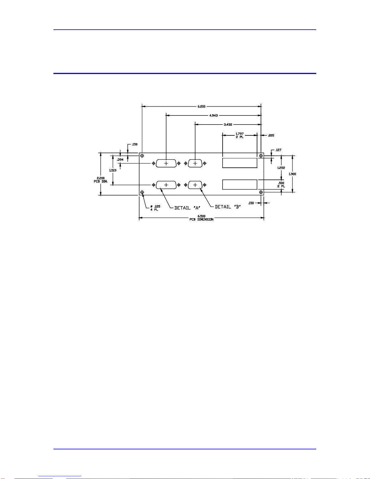
BOARD LAYOUT
ACC-8F Layout
Board Layout
5
Page 10
ACC-8F & ACC-8FP Delta Tau Data Systems, Inc.
ACC-8FP Layout
6
Board Layout
Page 11

Delta Tau Data Systems, Inc. ACC-8F & ACC-8FP
CONNECTORS AND JUMPERS
Connector Summary
JMACH1
Top View
JMACH1 is a 100-pin high-density header that provides the connection to the matching 100-pin header on
the PMAC2. It contains all of the input and output signals for the 2 axes between the ACC-8F board and
the PMAC2.
Pin # Symbol Function Description Notes
1 +5V Output/ Input +5V Power For external circuit or from ext.
supply
2 +5V Output/Input +5V Power For external circuit or from ext.
supply
3 GND Common Reference Voltage
4 GND Common Reference Voltage
5 CHA1+ Output Enc 1 Pos. A Chan. Also pulse input
6 CHA1- Output Enc 1 Neg. A Chan. Also pulse input
7 CHB1+ Output Enc 1 Pos. B Chan. Also direction input
8 CHB1- Output Enc 1 Neg. B Chan. Also direction input
9 CHC1+ Output Enc 1 Pos. C Chan. Index channel
10 CHC1- Output Enc 1 Neg. C Chan. Index channel
11 CHU1 Output Chan 1 U Flag Hall Effect, fault code, or sub-count
12 CHV1 Output Chan 1 V Flag Hall Effect, fault code, or sub-count
13 CHW1 Output CHAN 1 W FLAG Hall Effect, fault code, or sub-count
14 CHT1 Output Chan 1 T Flag Fault code, or sub-count
15 USER1 Output General Purpose User
Flag
16 PLIM1 Output Positive Overtravel
Hardware capture flag, or sub-count
Hardware capture flag
Limit
17 MLIM1 Output Negative Overtravel
Hardware capture flag
Limit
18 HOME1 Output Home Switch Input Hardware capture flag
19 ACCFLT1 Output Accessory Fault Flag For loss of acc supply voltage
JMACH1 (Continued)
Connectors and Jumpers
7
Page 12

ACC-8F & ACC-8FP Delta Tau Data Systems, Inc.
Pin # Symbol Function Description Notes
20 WD0/ Input Watchdog Output Low Is PMAC watchdog fault
21
22 SCLK12- Input/Output Encoder Sample Clock Direction Controlled By Pmac2
23 ADC_CLK1+ Input A/D Converter Clock Programmable frequency
24 ADC_CLK1- Input A/D Converter Clock Pr ogrammable frequency
25 ADC_STB1+ Input A/D Converter Strobe Programmable sequence
26 ADC_STB1- Input A/D Converter Strobe Programmable sequence
27 ADC_DAA1+ Output Chan A ADC Serial
28 ADC_DAA1- Ou tput Chan A ADC Serial
29 ADC_DAB1+ Output Chan B ADC Serial Data MSB first
30 ADC_DAB1- Output Chan B ADC Serial Data MSB first
31 AENA1+ Input Amplifier Enable High Is enable
32 AENA1- Input Amplifier Enable Low Is enable
33 FAULT1+ Output Amplifier Fault Programmable polarity
34 FAULT1- Output Amplifier Fault Programmable polarity
SCLK12+ Input/Output Encoder Sample Clock Direction Controlled By Pmac2
Jumper
Jumper
MSB first
Data
MSB first
Data
35 PWMATOP1+
DAC_CLK1+
36 PWMATOP1-
DAC_CLK1-
37 PWMABOT1+
DAC1A+
38 PWMABOT1-
DAC1A-
39 PWMBTOP1+
DAC_STB1+
40 PWMBTOP1-
DAC_STB1-
Input Phase A Top Cmd. Or
Dac Clock
Input Phase A Top Cmd. Or
Dac Clock
Input Phase A Bottom Cmd.
Or Dac A Serial Data
Input Phase A Bottom Cmd.
Or Dac A Serial Data
Input Phase B Top Cmd. Or
Dac Strobe
Input Phase B Top Cmd. Or
Dac Strobe
Programmable function control
Programmable function control
Programmable function control
Programmable function control
Programmable function control
Programmable function control
JMACH1 (Continued)
Pin # Symbol Function Description Notes
8
Connectors and Jumpers
Page 13

Delta Tau Data Systems, Inc. ACC-8F & ACC-8FP
41 PWMBBOT1+
DAC1B+
42 PWMBBOT1-
DAC1B-
43 PWMCTOP1+
DIR1+
44 PWMCTOP1-
DIR1-
45 PWMCBOT1+
PULSE1+
46 PWMCBOT1-
PULSE147 GND Common Reference Voltage
48 GND Common Reference Voltage
49 +5V Output / Input +5V Power For external circuit or from ext.
50 +5V Output / Input +5V Power For external circuit or from ext.
Input Phase B Bottom Cmd.
Or Dac B Serial Data
Input Phase B Bottom Cmd.
Or Dac B Serial Data
Input Phase B Top Cmd. Or
Pfm Direction
Input Phase B Top Cmd. Or
Pfm Direction
Input Phase B Bottom Cmd.
Or Pfm Pulse
Input Phase B Bottom Cmd.
Or Pfm Pulse
Programmable function control
Programmable function control
Programmable function control
Programmable function control
Programmable function control
Programmable function control
supply
supply
51 +5V Output / Input +5V Power For external circuit or from ext.
supply
52 +5V Output / Input +5V Power For external circuit or from ext.
supply
53 GND Common Reference Voltage
54 GND Common Reference Voltage
55 CHA2+ Output Enc 2 Pos. A Chan. Also pulse input
56 CHA2- Output Enc 2 Neg. A Chan. Also pulse input
57 CHB2+ Output Enc 2 Pos. B Chan. Also direction input
58 CHB2- Output Enc 2 Neg. B Chan. Also direction input
59 CHC2+ Output Enc 2 Pos. C Chan. Index channel
60 CHC2- Output Enc 2 Neg. C Chan. Index channel
61 CHU2 Output Chan 2 U Flag Hall Effect, fault code, or sub-count
62 CHV2 Output Chan 2 V Flag Hall Effect, fault code, or sub-count
63 CHW2 Output Chan 2 W Flag Hall Effect, fault code, or sub-count
JMACH1 (Continued)
Pin # Symbol Function Description Notes
Connectors and Jumpers
9
Page 14

ACC-8F & ACC-8FP Delta Tau Data Systems, Inc.
64 CHT2 Output Chan 2 T Flag Fault code, or sub-count
65 USER2 Output General Purpose
User Flag
66 PLIM2 Output Positive Overtravel
Limit
67 MLIM2 Output Negative Overtravel
Limit
68 HOME2 Output Home Switch Input Hardware capture flag
69 ACCFLT2 Input Accessory Fault Flag For loss of acc. supply voltage
70 WD0/ Output Watchdog Output Low Is PMAC Watchdog Fault
71 SCLK12+ Input/Output Encoder Sample Clock Direction Controlled By PMAC2
72 SCLK12- Input/Output Encoder Sample Clock Direction Controlled By PMAC2
73 ADC_CLK2+ Input A/D Converter Clock Programmable frequency
74 ADC_CLK2- Input A/D Converter Clock Pr ogrammable frequency
75 ADC_STB2+ Input A/D Converter Strobe Programmable sequence
76 ADC_STB2- Input A/D Converter Strobe Programmable sequence
77 ADC_DAA2+ Output Chan A ADC Serial
Data
Hardware capture flag, or sub-count
Hardware capture flag
Hardware capture flag
Jumper
Jumper
MSB first
78 ADC_DAA2- Ou tput Chan A ADC Serial
Data
79 ADC_DAB2+ Output Chan B ADC Serial Data MSB first
80 ADC_DAB2- Output Chan B ADC Serial Data MSB first
81 AENA2+ Input Amplifier Enable High Is enable
82 AENA2- Input Amplifier Enable Low Is enable
83 FAULT2+ Output Amplifier Fault Programmable polarity
84 FAULT2- Output Amplifier Fault Programmable polarity
85 PWMATOP2+
DAC_CLK2+
86 PWMATOP2-
DAC_CLK2-
Input Phase A Top Cmd. Or
Dac Clock
Input Phase A Top Cmd. Or
Dac Clock
MSB first
Programmable function control
Programmable function control
JMACH1 (Continued)
Pin # Symbol Function Description Notes
10
Connectors and Jumpers
Page 15

Delta Tau Data Systems, Inc. ACC-8F & ACC-8FP
87 PWMABOT2+
DAC2A+
88 PWMABOT2-
DAC2A-
89 PWMBTOP2+
DAC_STB2+
90 PWMBTOP2-
DAC_STB2-
91 PWMBBOT2+
DAC2B+
92 PWMBBOT2-
DAC2B-
93 PWMCTOP2+
DIR2+
94 PWMCTOP2-
DIR2-
95 PWMCBOT2+
PULSE2+
Input Phase A Bottom Cmd.
Or Dac A Serial Data
Input Phase A Bottom Cmd.
Or Dac A Serial Data
Input Phase B Top Cmd. Or
Dac Strobe
Input Phase B Top Cmd. Or
Dac Strobe
Input Phase B Bottom Cmd.
Or Dac B Serial Data
Input Phase B Bottom Cmd.
Or Dac B Serial Data
Input Phase B Top Cmd. Or
Pfm Direction
Input Phase B Top Cmd. Or
Pfm Direction
Input Phase B Bottom Cmd.
Or Pfm Pulse
Programmable function control
Programmable function control
Programmable function control
Programmable function control
Programmable function control
Programmable function control
Programmable function control
Programmable function control
Programmable function control
96 PWMCBOT2-
PULSE2-
Input Phase B Bottom Cmd.
Or Pfm Pulse
Programmable function control
97 GND Common Reference Voltage
98 GND Common Reference Voltage
99 +5V Output / Input +5V Power For external circuit or from ext.
supply
100 +5V Output / Input +5V Power For external circuit or from ext.
supply
The cable-to-board connector is from AMP with 0.025 Centerline ribbon cable. This is the AMPMODU
System 50 ribbon connector and the part number specified by AMP is 1-111196-6.
The maximum length specified by Delta Tau is 18 inches.
Connectors and Jumpers
11
Page 16

ACC-8F & ACC-8FP Delta Tau Data Systems, Inc.
1
J1 10-Pin IDC Header
Top View
Pin#
1 CHA1+ Input Enc 1 Pos. A Chan. Also pulse Input
2 ENCPWR Output Digital Supply Volt. Power for encoder
3 GND Common Reference Voltage
4 CHA1- Input Enc 1 Neg. A Chan. Also pulse Input
5 CHB1- Input Enc 1 Neg. B Chan. Also direction Input
6 GND Common Reference Voltage
7 ENCPWR Output Digital Supply Volt. Power for encoder
8 CHB1+ Input Enc 1 Pos. B Chan. Also direction Input
9 ENCPWR Output Digital Supply Volt. Power for encoder
10 CHC1+ Input Enc 1 Pos. C Chan. Index channel
A 10-pin IDC header for connection to 1st encoder in HP-compatible pinout. This header provides the
connection to a single quadrature encoder or the signals simulated for one from an amplifier or accessory
board. The signals on this connector are also available on TB2.
Symbol Function Description Notes
12
Connectors and Jumpers
Page 17

Delta Tau Data Systems, Inc. ACC-8F & ACC-8FP
1
J2 10-Pin IDC Header
Top View
Pin# Symbol Function Description Notes
1 CHA2+ Input Enc 2 Pos. A Chan. Also pulse Input
2 ENCPWR Output Digital Supply Volt. Power for encoder
3 GND Common Reference Voltage
4 CHA2- Input Enc 2 Neg. A Chan. Also pulse Input
5 CHB2- Input Enc 2 Neg. B Chan. Also direction Input
6 GND Common Reference Voltage
7 ENCPWR Output Digital Supply Volt. Power for encoder
8 CHB2+ Input Enc 2 Pos. B Chan. Also direction Input
9 ENCPWR Output Digital Supply Volt. Power for encoder
10 CHC2+ Input Enc 2 Pos. C Chan. Index channel
A 10-pin IDC header for connection to 2nd encoder in HP-compatible pinout. It provides the connection to
a single quadrature encoder or simulated signals from an amplifier or accessory board. Signals on this
connector are also available on TB3.
Connectors and Jumpers
13
Page 18

ACC-8F & ACC-8FP Delta Tau Data Systems, Inc.
1
J3 10-Pin IDC Header
Top View
Pin# Symbol Function Description Notes
1 CHA1+ Input Enc 1 Pos. A Chan Single ended input
2 CHB1+ Input Enc 1 Pos. B Chan Single ended input
3 CHC1+ Input Enc 1 Pos. C Chan Single ended input
4 CHA2+ Input Enc 2 Pos. A Chan Single ended input
5 CHB2+ Input Enc 2 Pos. B Chan Single ended input
6 CHC2+ Input Enc 2 Pos. C Chan Single ended input
7 GND Common Reference Signal
8 GND Common Reference Signal
9 SCLK12+ Output Encoder Sample Clock
10 CLOCK Output DAC_CLK or
ADC_CLK
A 10-pin IDC header for connection of encoder inputs for both channels (single ended). It provides
connection to single-ended quadrature encoder inputs for two axes. It also provides connection to
ADC_CLK or DAC_CLK signals to accessories such as ACC-8D option 8.
E22 jumper selects
14
Connectors and Jumpers
Page 19

Delta Tau Data Systems, Inc. ACC-8F & ACC-8FP
1
J4 14-Pin IDC Header
Top View
Pin# Symbol Function Description Notes
1 CHT1 Input Supplementary Flag T Fault code, or sub-count
2 NC No Connect
3 CHU1 Input Supplementary Flag U Hall Effect, fault code, or sub-
count
4 CHV1 Input Supplementary Flag V Hall Effect, fault code, or sub-
count
5 CHW1 Input Supplementary Flag W Hall Effect, fault code, or sub-
count
6 USER1 Input General Purpose
User Flag
7 CHT2 Input Supplementary Flag T Fault Code, Or Sub-Count
8 NC No Connect
9 CHU2 Input Supplementary Flag U Hall Effect, fault code, or sub-
10 CHV2 Input Supplementary Flag V Hall Effect, fault code, or sub-
11 CHW2 Input Supplementary Flag W Hall Effect, fault code, or sub-
12 USER2 Input General Purpose
User Flag
13 GND Common Reference Voltage
14 +5V Output Supply Voltage
A 14-pin IDC header for connection to supplementary input flags for both channels. This header provides
the connection to supplemental input flags that can be used for sub-count interpolation, hall-effect
commutation, or amplifier fault codes. The USER flags can also be input on TB4 or TB5.
Hardware capture flag, or subcount
count
count
count
Hardware capture flag, or sub-
count
Connectors and Jumpers
15
Page 20

ACC-8F & ACC-8FP Delta Tau Data Systems, Inc.
5
8
1
P1 DB15-pin Connector
1
9
Top View
Pin # Symbol Function Description Notes
1 ENCPWR Output Digital Supply Power for encoder
2 GND Common Digital Reference
3 CHA1+ Input Enc 1 Pos. A Chan. Also pulse input
4 CHB1+ Input Enc 1 Pos. B Chan. Also direction input
5 CHC1+ Input Enc 1 Pos. C Chan. Index channel
6 CHU1+ Input Supplemental Flag U
7 CHW1+ Input Supplemental Flag W
8 GND Common Digital Reference
9 ENCPWR Output Digital Supply Power for encoder
10 GND Common Digital Reference
11 CHA1- Input Enc 1neg. A Chan. Also pulse Input
12 CHB1- Input Enc 1 Neg. B Chan. Also direction input
13 CHC1- Input Enc 1 Neg. C Chan. Index channel
14 CHV1+ Input Supplemental Flag V
15 CHT1+ Input Supplemental Flag T
A DB 15 connector for discrete-wired connection to the 1st encoder and Supplemental Flags. This connector
alternately provides the interface to a single quadrature encoder or the signals of a simulated encoder. It
additionally provides connection to the set of supplemental flags for that motor.
16
Connectors and Jumpers
Page 21

Delta Tau Data Systems, Inc. ACC-8F & ACC-8FP
P2 DB15-pin Connector
8
15
1
9
Top View
Pin # Symbol Function Description Notes
1 ENCPWR Output Digital Supply Power for encoder
2 GND Common Digital Reference
3 CHA2+ Input Enc 2 Pos. A Chan. Also pulse input
4 CHB2+ Input Enc 2 Pos. B Chan. Also direction input
5 CHC2+ Input Enc 2 Pos. C Chan. Index channel
6 CHU2+ Input Supplemental Flag U
7 CHW2+ Input Supplemental Flag W
8 GND Common Digital Reference
9 ENCPWR Output Digital Supply Power for encoder
10 GND Common Digital Reference
11 CHA2- Input Enc 2 Neg. A Chan. Also pulse input
12 CHB2- Input Enc 2 Neg. B Chan. Also direction input
13 CHC2- Input Enc 2 Neg. C Chan. Index channel
14 CHV2+ Input Supplemental Flag V
15 CHT2+ Input Supplemental Flag T
A DB 15 connector for discrete-wired connection to 2nd encoder and Supplemental Flags. This connector
alternately provides the interface to a single quadrature encoder or the signals of a simulated encoder. It
additionally provides connection to the set of supplemental flags for that motor.
Connectors and Jumpers
17
Page 22

ACC-8F & ACC-8FP Delta Tau Data Systems, Inc.
P3 DB9-pin Connector
5
9
1
6
Top View
Pin # Symbol Function Description Notes
1 USER1 Input General Capture Flag Sinking or sourcing
2 MLIM1 Input Negative Limit Fla g Sinking or sourcing
3 FL_RT1 Input Return For All Flags +V (12 To 24 V) Or 0 V
4 FLGRET Output Flag Return 12/25 V Rreturn from TB3
5 AGND Ground Analog Common
6 PLIM1 Input Positive Limit Flag Sinking or sourcing
7 HOME1 Input Home Flag Sinking or sourcing
8 FLGPWR Output Flag Power + 12/25 V from TB3
9 AGND Ground Analog Common
A DB 9 connector for connection to main flags of the 1st channel (home, limits, & user). This connector
provides alternate connection for the standard machine input flags for an axis. The USER flag can also be
brought in on J4 or TB4.
P4 DB9-pin Connector
5
9
1
6
Top View
Pin # Symbol Function Description Notes
1 USER2 Input General Capture Flag Sinking or sourcing
2 MLIM2 Input Negative Limit Fla g Sinking or sourcing
3 FL_RT2 Input Return For All Flags +V (12 to 24 V) or 0 V
4 FLGRET Output Flag Return 12/25 V return from TB3
5 AGND Ground Analog Common
6 PLIM2 Input Positive Limit Flag Sinking or sourcing
7 HOME2 Input Home Flag Sinking or sourcing
8 FLGPWR Output Flag Power + 12/25 V From TB3
9 AGND Ground Analog Common
A DB 9 connector for connection to main flags of the 2nd channel (home, limits, & user). This connector
provides alternate connection for the standard machine input flags for an axis. The USER flag can also be
brought in on J4 or TB5.
18
Connectors and Jumpers
Page 23

Delta Tau Data Systems, Inc. ACC-8F & ACC-8FP
P5 36-pin Mini-D Connector
Top View
Pin # Symbol Function Description Notes
1 FC0 Feedback 1 Of 4 Fault Code Bits Optional
2 FC2 Feedback 1 Of 4 Fault Code Bits Optional
3 ADC_CLK1+ Command A/D Converter Clock
4 ADC_STB1+ Command A/D Converter Strobe
5 CURRENTA+ Feedback Phase A Actual Current
Data
6 CURRENTB+ Feedback Phase B Actual Current
Data
7 AENA1+ Command Amplifier Enable High is enable
8 FAULT1+ Feedback Amplifier Fault High is fault
9 PWMATO P1+ Command Phase A Top Cmd High is On command
10 PWMAB OT1+ Command Phase A Bottom Cmd High is On command
11 PWMBTOP1+ Command Phas e B Top Cmd High is On command
12 PWMBBOT 1+ C ommand Phase B Bottom Cmd High is On command
13 PWMCTOP1+ Command Phase C Top Cmd High is On command
Serial digital
Serial digital
14 PWMCBOT1+ Command Phase C Bottom Cmd Hig h is On comma nd
15 GND Common Reference Voltage
16 +5V Power +5v Power From controller
17 RESERVED
18 RESERVED
19 FC1 Feedback 1 Of 4 Fault Code Bits Optional
20 FC3 Feedback 1 Of 4 Fault Code Bits Optional
21 ADC_CLK1- Co mmand A/D Converter Clock
22 ADC_STB1- Command A/D Converter Strobe
23 CURRENTA- Feedback Phase A Actual Current
Data
24 CURRENTB- Feedback Phase B Actual Current
Data
25 AENA1- Command Amplifier Enable Low is enable
26 FAULT1- Feedback Amplifier Fault Low is fault
27 PWMATOP1- Command Phase A Top Cmd Low is On command
Serial digital
Serial digital
Connectors and Jumpers
19
Page 24

ACC-8F & ACC-8FP Delta Tau Data Systems, Inc.
P5 (Continued)
Pin # Symbol Function Description Notes
28 PWMAB OT1- Command Phase A Bott om Cmd Low is On command
29 PWMBTOP1- Command Phase B Top Cmd Low is On command
30 PWMBBOT 1- Command Phase B Bottom Cmd Low i s On command
31 PWMCTOP1- Command Phase C Top Cmd Low is On command
32 PWMCBOT1- Command Phase C Bottom Cmd Low i s On command
33 GND Common Reference Voltage
34 +5V Power +5v Power From controller
35 RESERVED
36 RESERVED
A mini-D 36-pin connector for 1st digital amplifier command outputs and current feedbacks. This
connector provides the interface to a fully digital amplifier for the first channel. Note that current feedback
data must be in serial digital form, already converted from analog in the amplifier.
P6 36-pin Mini-D Connector
Top View
Pin # Symbol Function Description Notes
1 FC0 Feedback 1 Of 4 Fault Code Bits Optional
2 FC2 Feedback 1 Of 4 Fault Code Bits Optional
3 ADC_CLK2+ Command A/D Converter Clock
4 ADC_STB2+ Command A/D Converter Strobe
5 CURRENTA+ Feedback Phase A Actual Current
Data
6 CURRENTB+ Feedback Phase B Actual Current
Data
7 AENA2+ Command Amplifier Enable High is enable
8 FAULT2+ Feedback Amplifier Fault High is fault
9 PWMATO P2+ Command Phase A Top Cmd High is On command
10 PWMAB OT2+ Command Phase A Bottom Cmd High is On command
11 PWMBTOP2+ Command Phas e B Top Cmd High is On command
12 PWMBBOT 2+ C ommand Phase B Bottom Cmd High is On command
Serial digital
Serial digital
13 PWMCTOP2+ Command Phase C Top Cmd High is On command
14 PWMCBOT2+ Command Phase C Bottom Cmd Hig h is On comma nd
20
Connectors and Jumpers
Page 25

Delta Tau Data Systems, Inc. ACC-8F & ACC-8FP
P6 (Continued)
Pin # Symbol Function Description Notes
15 GND Common Reference Voltage
16 +5V Power +5v Power From controller
17 RESERVED
18 RESERVED
19 FC1 Feedback 1 Of 4 Fault Code Bits Optional
20 FC3 Feedback 1 Of 4 Fault Code Bits Optional
21 ADC_CLK2- Co mmand A/D Converter Clock
22 ADC_STB2- Command A/D Converter Strobe
23 CURRENTA- Feedback Phase A Actual Current
Data
24 CURRENTB- Feedback Phase B Actual Current
Data
25 AENA2- Command Amplifier Enable Low is enable
26 FAULT2- Feedback Amplifier Fault Low is fault
27 PWMATOP2- Command Phase A Top Cmd Low is On command
28 PWMAB OT2- Command Phase A Bott om Cmd Low is On command
29 PWMBTOP2- Command Phase B Top Cmd Low is On command
30 PWMBBOT 2- Command Phase B Bottom Cmd Low i s On command
31 PWMCTOP2- Command Phase C Top Cmd Low is On command
32 PWMCBOT2- Command Phase C Bottom Cmd Low i s On command
33 GND Common Reference Voltage
34 +5V Power +5v Power From controller
35 RESERVED
36 RESERVED
A mini-D 36-pin connector for 2nd digital amplifier command outputs and current feedbacks. This
connector provides the interface to a fully digital amplifier for the second channel. Note that current
feedback data must be in serial digital form, already converted from analog in the amplifier.
Serial digital
Serial digital
Connectors and Jumpers
21
Page 26

ACC-8F & ACC-8FP Delta Tau Data Systems, Inc.
TB1 12 Point Terminal Block
1 12
Pin # Symbol Function Description Notes
1 CHA1+ Input Enc 1 Pos. A Chan. Also pulse input
2 CHA1- Input Enc 1 Neg. A Chan. Also pulse input
3 CHB1+ Input Enc 1 Pos. B Chan. Also direction input
4 CHB1- Input Enc 1 Neg. B Chan. Also direction input
5 CHC1+ Input Enc 1 Pos. C Chan. Index channel
6 CHC1- Input Enc 1 Ne g. C Chan. Index channel
7 ENCPWR Output Digital Supply Power for encoder
8 GND Common Digital Reference
9 CHU1+ Input Supplemental Flag U
10 CHV1+ Input Supplemental Flag V
11 CHW1+ Input Supplemental Flag W
12 CHT1+ Input Supplemental Flag T
A 12-point terminal block for discrete-wired connection to 1st encoder and Supplemental Flags. This
terminal block provides the interface to a single quadrature encoder or the signals of a simulated encoder.
It additionally provides connection to the set of supplemental flags for that motor.
22
Connectors and Jumpers
Page 27

Delta Tau Data Systems, Inc. ACC-8F & ACC-8FP
TB2 12 Point Terminal Block
1 12
Pin # Symbol Function Description Notes
1 CHA2+ Input Enc 2 Pos. A Chan. Also pulse input
2 CHA2- Input Enc 2 Neg. A Chan. Also pulse input
3 CHB2+ Input Enc 2 Pos. B Chan. Also direction input
4 CHB2- Input Enc 2 Neg. B Chan. Also direction input
5 CHC2+ Input Enc 2 Pos. C Chan. Index channel
6 CHC2- Input Enc 2 Ne g. C Chan. Index channel
7 ENCPWR Output Digital Supply Power for encoder
8 GND Common Digital Reference
9 CHU2+ Input Supplemental Flag U
10 CHV2+ Input Supplemental Flag V
11 CHW2+ Input Supplemental Flag W
12 CHT2+ Input Supplemental Flag T
A 12-point terminal block for discrete-wired connection to 2nd encoder and Supplemental Flags. This
terminal block provides the interface to a single quadrature encoder or the signals of a simulated encoder. It
additionally provides connection to the set of supplemental flags for that motor.
TB3 6 Point Terminal Block
Pin # Symbol Function Description Notes
1 GND Common Reference Voltage Tied to PMAC2 ground
2 +5V Input Positive Supply Voltage See Above
3 +12/25V Input Flag Power For Optical Isolation
4 12/25V Rtrn Input Flag Return For Optical Isolation
5 AGND Input Analog Ground
6 AGND Input Analog Ground
A 6-point terminal block for optional +5V power supply connection for accessory board. This terminal
block provides the input for the power supply for the circuits on the board. If jumper E1is ON, the +5V
supply for the board will come from the PMAC2 and a separa te +5V supply should not be brought in here.
Connectors and Jumpers
1 6
23
Page 28

ACC-8F & ACC-8FP Delta Tau Data Systems, Inc.
TB4 8 Point Terminal Block
1 8
Pin # Symbol Function Description Notes
1 USER1 Input General Capture Flag Sinking or sourcing
2 PLIM1 Input Positive Limit Flag Sinking or sourcing
3 MLIM1 Input Negative Limit Fla g Sinking or sourcing
4 HOME1 Input Home Flag Sinking or sourcing
5 FLG_1_RET Input Return For All Flags +V (12 To 24v) or 0v
6 AGND Ground Analog Common
7 FLGPWR Output Flag Power +12/25 V from TB6
8 FLGRTN Output Flag Return 12/25 V return from TB3
An 8-point terminal block for connection to main flags of the 1st channel (home, limits, & user). This terminal
block provides the conne ction for the st andard machine input flags for an axi s . The USER fla g can also be b rought
in on J4 or P3.
TB5 8 Point Terminal Block
1 8
Pin # Symbol Function Description Notes
1 USER2 Input General Capture Flag Sinking or sourcing
2 PLIM2 Input Positive Limit Flag Sinking or sourcing
3 MLIM2 Input Negative Limit Fla g Sinking or sourcing
4 HOME2 Input Home Flag Sinking or sourcing
5 FLG_2_RET Common Return For All Flags +V (12 T o 24v) or 0v
6 AGND Ground Analog Common
7 FLGPWR Output Flag Power +12/25 V from TB6
8 FLGRTN Output Flag Return 12/25 V return from TB3
An 8-point terminal block for connection to main flags of the 2nd channel (home, limits, & user). This terminal
block provides the conne ction for the st andard machine input flags for an axi s . The USER fla g can also be b rought
in on J4 or P4.
24
Connectors and Jumpers
Page 29

Delta Tau Data Systems, Inc. ACC-8F & ACC-8FP
Jumper Summary
Refer to the ACC-8F layout diagram for jumper locations.
Jumper Configuration Description Default
E1
If more than
Jump 1 to 2 to use +5V input from
PMAC2 to power encoders.
250mA
isused
through the
ACC-8F, the
+5V power
must be
brought in via
TB3 and E1
must be
removed.
E2 - E13 Jump 1 to 2 when an encoder with a
single index pulse on the channel C or Z
is used.
Jump 2 to 3 when using an encoder with
U, V, W, T and Index signals encoded on
the C channel (i.e. Yaskawa multiplexed
encoder).
E14 - E19 Jump 1 to 2 to connect the shell of
connectors P1, P2, P3, P4, P5 and P6 to
Analog ground.
1 to 2
1 to 2
1 to 2
E21 Jump 1 to 2 if amplifier FLT1+ line (P5-
8) is normally high (No fault)
Jump 2 to 3 if amplifier FLT1- line (P5-
26)is normally high.(No fault)
If the amplifier fault condition code is not
required at PMAC2, remove E21.
E22 Jump 1 to 2 to provide
ATOP1+/DAC_CLK to pin 10 on J3
Jump 2 to 3 to provide ADC_CLK to pin
10 on J3.
Connectors and Jumpers
1 to 2
1 to 2
25
Page 30

ACC-8F & ACC-8FP Delta Tau Data Systems, Inc.
Jumper Summary (Continued)
Jumper Configuration Description Default
E23 Jump 1 to 2 if amplifier FLT2+ line (P6-
8) is normally high (No fault)
Jump 2 to 3 if amplifier FLT2- line (P6-
26) is normally high.(No fault)
If the amplifier fault condition code is not
required at PMAC2, remove E21.
E24
The E24
jumper is
used on
602775-103
revision and
Jump 1 to 2 when an encoder with a
single index pulse on the channel C or Z
is used.
Jump 2 to 3 when connecting an encoder
with power-on information (i.e. Yaskawa
multiplexed encoder).
newer.
1 to 2
1 to 2
26
Connectors and Jumpers
Page 31

Date: April 30, 1997 Sheet 1 of 1
Size Document Number REV
D 602775-323 A
Title
ACC-8F,PMAC-2 INT. 36 PIN
NORTHRIDGE CA 91324
9036 WINNETKA AVE
DELTA TAU DATA SYSTEMS INC.
1
2
3
4
5
6
7
8
9
10
J3
H10\BOX
ENCODER 1
10-PIN BOX
8
15
7
14
6
13
5
12
4
11
3
10
2
9
1
1
6
P1
DB15S
1
2
3
4
5
6
7
8
9
10
J1
HEADER 10
CHA1+
CHA1CHB1-
CHB1+
C1+
+5V
GND
PROGRAMMING
ISPLSI
1
2
3
4
5
6
7
8
JP1
8 HEADER
C10
.01
SDO
SDI
ISPEN-
VCC
1
23456789
1
0
RP8
10K
VCC VCC
2-3 YASKAWA ENCODERS
1-2 STANDARD ENCODERS
1ST AXIS ENCODER SELECTION
THIS DOCUMENT IS THE CONFIDENTIAL PROPERTY OF DELTA TAU
DATA SYSTEMS INC. AND IS LOANED SUBJECT TO RETURN UPON
DEMAND. TITLE TO THIS DOCUMENT IS NEVER SOLD OR
TRANSFERRED FOR ANY REASON. THIS DOCUMENT IS TO BE USED
ONLY PURSUANT TO WRITTEN LICENSE OR WRITTEN INSTRUCTIONS
OF DELTA TAU DATA SYSTEMS INC. ALL RIGHTS TO DESIGNS AND
INVENTIONS ARE RESERVED BY DELTA TAU DATA SYSTEMS INC.
POSSESSION OF THIS DOCUMENT INDICATES ACCEPTANCE OF THE
ABOVE AGGREEMENT.
1 2
3 4
5 6
7 8
9 10
11 12
13 14
15 16
17 18
19 20
21 22
23 24
25 26
27 28
29 30
31 32
33 34
35 36
37 38
39 40
41 42
43 44
45 46
47 48
49 50
51 52
53 54
55 56
57 58
59 60
61 62
63 64
65 66
67 68
69 70
71 72
73 74
75 76
77 78
79 80
81 82
83 84
85 86
87 88
89 90
91 92
93 94
95 96
97 98
99 100
JMACH1
HEADER 50X2
CHA1-CHA1+
CHB1+ CHB1-
CHC1-CHC1+
CHU1+
CHW1+
USER1+
MLIM1+
CHV1+
CHT1+
PLIM1+
HOME1+
ACLK1+ ACLK1ASTB1+ ASTB1ADAA1+ ADAA1ADAB1+ ADAB1-
ATOP1+
ABOT1+
BTOP1+
BBOT1+
CTOP1+
CBOT1+
FLT1+
ENA1+ ENA1-
FLT1-
ATOP1-
ABOT1-
BTOP1-
BBOT1-
CTOP1-
CBOT1-
SCK12+ SCK12-
AFLT1+ WDO-
GND GND
FAULT
2
3
1
E6
2
3
1
E5
2
3
1
E7
2
3
1
E21
YU1+
U1+
YV1+
V1+
YW1+
W1+
FLT1-
FLT1+
CHU1
CHV1
CHW1
FC1-A
FC1-B
FC1-C
FC1-D
CHT1
1A
2
1B
3
2A
5
2B
6
3A
11
3B
10
4A
14
4B
13
G
15
A/B
1
1Y
4
2Y
7
3Y
9
4Y
12
U10
74HC257
R1
10K
C4 .1UF
CHU1+
CHV1+
CHW1+
CHT1+
VCC
GND
GND
ISPEN
7
SDI
8
SDO
18
SCLK
27
MODE
30
V
C
C
6
V
C
C
2
8
G
N
D
3
9
G
N
D
1
7
A1
9
B1
10
YU1+
31
YV1+
32
YW2+
37
Z2
38
YV2+
36
YU2+
35
YW1+
33
Z1
34
C1
11
A2
13
B2
14
C2
15
Y0-CLK
5
U11
ISPLSI2032
INA
1
INA
2
INB
15
INB
14
INC
7
INC
6
IND
9
IND
10
ENAC
4
ENBD
12
OUTD
11
OUTC
5
OUTB
13
OUTA
3
U4
MC34C86
A1
B1
C1
CHA1+
CHB1+
CHB1-
CHA1-
SCLK
MODE
ISPEN-
GND
(REMOVE PIN 5)
HEADER
C18 .1UF
YU1+
VCC
GND
SHELL
1
2
3
4
5
6
7
8
9
10
11
12
TB1
TB12\150
2
3
1
E2
E16
CHA1+
CHA1CHB1+
YC1+
CHA1+
CHA1CHB1+
CHB1C1+
C1U1+
V1+
W1+
CHT1
ENCPWR
ENCPWR
GND
GND
GND
DAC_CLK1+
FOR 8T
OPT-02, OPT03
DSUB CONN
ENCODER 1
ATOP1+
ACLK1-
CLOCK
ENCODER
DUAL INPUT
(SINGLE-ENDED)
36
18
35
17
34
16
33
15
32
14
31
13
30
12
29
11
28
10
27
9
26
8
25
7
24
6
23
5
22
4
21
3
20
2
19
1
3
7
P5
CONNECTOR HD36
2
3
1
E22
JMP3
FC1-A
FC1-B
FC1-C
FC1-D
CHA1+
CHB1+
CHC1+
CHA2+
CHB2+
CHC2+
GND
GND
SCK12+
1ST AXIS
AMPLIFIER
INTERFACE
ACLK1+
ACLK1ASTB1+
ASTB1ADAA1+
ADAA1ADAB1+
ADAB1-
FLT1+
FLT1ATOP1+
ATOP1ABOT1+
ABOT1BTOP1+
BTOP1BBOT1+
BBOT1CTOP1+
CTOP1CBOT1+
CBOT1-
ENA1-
ENA1+
OPT-01
TERM BLK
ENCODER 1
ENCODER 2
2
3
1
E3
1
2
3
4
5
6
7
8
9
10
J2
HEADER 10
CHB1C1+
C1-
CHC1-
CHC1+
YC1-
U1+
V1+
W1+
CHT1
CHA2+
CHA2CHB2-
+5V
GND
+5V
(TQFP)
YV1+
YW1+
YU2+
YV2+
YW2+
Z2
Z1
INA
1
INA
2
INB
15
INB
14
INC
7
INC
6
IND
9
IND
10
ENAC
4
ENBD
12
OUTD
11
OUTC
5
OUTB
13
OUTA
3
U5
MC34C86
C5 .1UF
A2
B2
C2
CHA2+
CHA2-
CHB2+
CHB2-
SCK12SCK12+
SCK12YC1-
YC1+
SDI
SDO
SCLK
MODE
VCC
VCC GND
1
3
D1
MMBD301LT1
4
3
5
9
10
8
1
12
K1
FBR12ND05
ENCPWR
VCC VCC
GNDGND
2
3
1 E24
JUMPER3
2-3 YASKAWA ENCODERS
1-2 STANDARD ENCODERS
1ST AND 2ND AXIS ENCODER SELECTION
POLARITY
A
1
B
2
CLK
8
CLR
9
QA
3
QB
4
QC
5
QD
6
QE
10
QF
11
QG
12
QH
13
U16
74ACT164
C25 .1UF
WDO-
SCK12
VCC GND
(SCK12+) (SCK12-)
(WDO-)
CHA2+
CHB2+
CHC2+
CHA2CHB2-
CHC2CHU2+
CHW2+
USER2+
MLIM2+
CHV2+
CHT2+
PLIM2+
HOME2+
ENA2+ ENA2-
FLT2-FLT2+
ATOP2+
ABOT2+
BTOP2+
BBOT2+
CTOP2+
CBOT2+
ATOP2-
ABOT2-
BTOP2-
BBOT2-
CTOP2-
CBOT2-
ACLK2+
ASTB2+
ADAA2+
ADAB2+
ACLK2-
ASTB2-
ADAA2-
ADAB2-
AFLT2+
GND
GND
GND
GND
PMAC2'S +5Vdc
+5VRET
+5VDC
12/25V
12/25VRET
D3
1N5908
C1
22 35V
F1
2A
E1
1
2
3
4
5
6
TB3
TB6\150
GND GND
GND
+5V
AGND
AGND
VCCFLGPWR
FLGRET
2-3 YASKAWA ENCODERS
1-2 STANDARD ENCODERS
2ND AXIS ENCODER SELECTION
2
3
1
E11
2
3
1
E12
2
3
1
E13
YU2+
U2+
YV2+
V2+
YW2+
W2+
FC2-A
CHU2
FC2-B
CHV2
FC2-C
CHW2
FC2-D
CHT2
1A
2
1B
3
2A
5
2B
6
3A
11
3B
10
4A
14
4B
13
G
15
A/B
1
1Y
4
2Y
7
3Y
9
4Y
12
U9
74HC257
1
23456789
1
0
RP7
10K
R2
10K
CHU2+
CHV2+
CHW2+
CHT2+
VCC VCC
GND
INA
1
INA
2
INB
15
INB
14
INC
7
INC
6
IND
9
IND
10
ENAC
4
ENBD
12
OUTD
11
OUTC
5
OUTB
13
OUTA
3
U12
MC34C86
1
2
3
U13A
74HC86
R4
6.81K
1%
C6 .1UF
YC2YC2+
VCC
VCC
VCC
VCC
GND
C21 .1UF
GND
VCC
8
15
7
14
6
13
5
12
4
11
3
10
2
9
1
1
6
P2
DB15S
CHA2+
CHA2CHB2+
CHB2C2+
C2-
W2+
V2+
U2+
CHT2
CHB2+
C2+
ENCPWR
ENCPWR
GND
GND
GND
OPT-02, OPT03
DSUB CONN
ENCODER 2
10-PIN BOX
SHELL
E15 JUMPER
GND
+5V
GND
DUAL AXIS
U,V,W,T & USER
FLAG INPUTS
1
2
3
4
5
6
7
8
9
10
11
12
13
14
J4
H14\BOX
USER1+
USER2+
CHT1
CHT2
U1+
V1+
W1+
U2+
V2+
W2+
GND
+5V
OPT-01
TERM BLK
SHELL
1
2
3
4
5
6
7
8
9
10
11
12
TB2
TB12\150
2
3
1
E8
2
3
1
E9
E17
CHA2+
CHA2CHB2+
CHB2C2+
C2-
CHC2+
CHC2-
YC2-
YC2+
W2+
V2+
U2+
CHT2
GND
+5V
GND
1
2
3
U15A
74HC132
R5
10K
4
5
6
U15B
74HC132
C23
.1UF
9
10
8
U15C
74HC132
R6
10K
12
13
11
U15D
74HC132
AFLT1+
AFLT2+
GND
C19 .1UF
4
5
6
U13B
74HC86
INA
1
INA
2
INB
15
INB
14
INC
7
INC
6
IND
9
IND
10
ENAC
4
ENBD
12
OUTD
11
OUTC
5
OUTB
13
OUTA
3
U14
MC34C86
9
10
8
U13C
74HC86 12
13
11
U13D
74HC86
VCC
VCC GND
C17 .1UF
OUTA
3
OUTA
2
INA
1
OUTB
5
OUTB
6
OUTC
11
OUTC
10
OUTD
13
OUTD
14
INB
7
INC
9
IND
15
ENAB
4
ENCD
12
U8
MC34C87
Z1
Z2
CHA1+
CHA1-
CHB1+
CHB1-
CHA2+
CHA2-
VCC
GND
GND
GND
FAULT
POLARITY
2
3
1
E23
CHC2-
CHC1+
CHC1-
FLT2-
FLT2+
USER SUPPLIED
POWER
1
1
M1
C11
.1UF
PC BOARD
MOUNTING
HOLES
1
1
M2
1
1
M3
1
1
M4
C12
.1UF
C15
.1UF
C16
.1UF
GND
CHC2+
ENCODER 1ENCODER 2
1-2 = REGULAR ENC (DISABLE Z INPUT)
2-3 = YASKAWA ENC (ENABLE Z INPUT)
2
3
1
E10
2
3
1
E4
C9 .1UF
CHB2+
CHB2-
VCC
GND
VCC
GND
VCC
GND
(2.05V)
C20 .1UF
C22
.1UF
R3
4.75K
1%
GND
VCC
VCC GND
C24
.1UF
ACI1A
1
ACI1B2E1
15
C1
16
ACI2A
3
ACI2B
4
ACI3A
5
ACI3B
6
ACI4A
7
ACI4B8E4
9
C4
10
E3
11
C3
12
E2
13
C2
14
U1
PS2705-4NEC-ND
1
2 3 4 5 6 7 8 9
1
0
RP1
SIP9C
1K
USER1+
PLIM1+
GND
SHELL
1 2RP3A 4.7K
3 4RP3B 4.7K
5 6RP3C 4.7K
7 8RP3D 4.7K
5
9
4
8
3
7
2
6
1
1
0
P3
DB9S
LIMITS1
E18 JUMPER
1
2
3
4
5
6
7
8
TB4
TB8\150
USER1
PLIM1
MLIM1
USER1
PLIM1
MLIM1
HOME1
FL_RT1
AGND
AGND
FLGPWR
FLGRET
OPT-02, OPT03
DSUB CONN
2ND AXIS
AMPLIFIER
INTERFACE
36
18
35
17
34
16
33
15
32
14
31
13
30
12
29
11
28
10
27
9
26
8
25
7
24
6
23
5
22
4
21
3
20
2
19
1
3
7
P6
CONNECTOR HD36
ACLK2+
ACLK2ASTB2+
ASTB2ADAA2+
ADAA2ADAB2+
ADAB2-
FLT2+
FLT2ATOP2+
ATOP2ABOT2+
ABOT2BTOP2+
BTOP2BBOT2+
ENA2-
ENA2+
FC2-A
FC2-B
FC2-C
FC2-D
SHELL
E14 JUMPER
BBOT2CTOP2+
CTOP2CBOT2+
CBOT2-
GND
+5V
GND
OPT-01
TERM BLK
OPT-02, OPT03
DSUB CONN
SHELL
1 2RP4A 4.7K
3 4RP4B 4.7K
5 6RP4C 4.7K
7 8RP4D 4.7K
1 2RP5A 4.7K
5
9
4
8
3
7
2
6
1
1
0
P4
DB9S
LIMITS2
E19 JUMPER
HOME1
FL_RT1
USER2
PLIM2
MLIM2
HOME2
FL_RT2
AGND
AGND
AGND
FLGPWR
FLGPWR
FLGRET
FLGRET
ACI1A
1
ACI1B2E1
15
C1
16
ACI2A
3
ACI2B
4
ACI3A
5
ACI3B
6
ACI4A
7
ACI4B8E4
9
C4
10
E3
11
C3
12
E2
13
C2
14
U2
PS2705-4NEC-ND
1
2 3 4 5 6 7 8 9
1
0
RP2
SIP9C
1K
MLIM1+
HOME1+
GND
NOTES:
1. C11-C16 CAPACITORS ARE INSTALLED IN CONJUNCTION WITH CE CERTIFICATION.
USER2+
PLIM2+
MLIM2+
HOME2+
GND
3 4RP5B 4.7K
5 6RP5C 4.7K
7 8RP5D 4.7K
1 2RP6A 4.7K
3 4RP6B 4.7K
5 6RP6C 4.7K
7 8RP6D 4.7K
1
2
3
4
5
6
7
8
TB5
TB8\150
USER2
PLIM2
MLIM2
HOME2
FL_RT2
AGND
FLGPWR
FLGRET
OPT-01
TERM BLK
Page 32

1
1
2
2
3
3
4
4
5
5
6
6
7
7
8
8
A A
B B
C C
D D
602765-322
B
ACC-8FP,DIGITAL AMP INTF, PNL MOUNT
DELTA TAU DATA SYSTEMS INC.
9036 WINNETKA AVE
D
1 1Monday, August 25, 1997
NORTHRIDGE CA 91324
Title
Size Document Number Rev
Date: Sheet of
ENCPWR
CHA1+
YC1+ CHA1-
CHB1+
CHC1+ CHB1SDO C1+
SDI C1ISPEN- YC1- U1+
V1+
MODE CHC1- W1+
CHT1
YU1+ SCLK
CHA1+ CHA1- U1+
CHB1+ CHB1CHC1+ CHC1CHU1+ CHV1+ YV1+
CHW1+ CHT1+ FC1-A CHU1+
USER1+ PLIM1+ V1+ CHU1
MLIM1+ HOME1+ FC1-B CHV1+
AFLT1+ WDO- CHV1
SCK12+ SCK12- YW1+ FC1-C CHW1+
ACLK1+ ACLK1- CHW1
ASTB1+ ASTB1- W1+ FC1-D CHT1+
ADAA1+ ADAA1- CHT1 CHA1ADAB1+ ADAB1- CHB1ENA1+ ENA1FLT1+ FLT1ATOP1+ ATOP1- CHB1+
ABOT1+ ABOT1- FLT1- CHA1- A1
BTOP1+ BTOP1- CHA1+ C1+ FC1-A
BBOT1+ BBOT1- FLT1+ B1 FC1-B
CTOP1+ CTOP1- CHB1- FC1-C
CBOT1+ CBOT1- CHB1+ C1 ISPEN- YU1+ FC1-D
SDI YV1+ ACLK1+
YC1- SCK12 SDO YW1+ ACLK1YC1+ SCLK Z1 ASTB1+
MODE ASTB1-
CHA2+ CHA2- SCK12- YU2+ ADAA1+
CHB2+ CHB2- SCK12+ YV2+ ADAA1CHC2+ CHC2- YW2+ ADAB1+
CHU2+ CHV2+ Z2 ADAB1-
CHW2+ CHT2+ ENA1+
USER2+ PLIM2+ ENA1MLIM2+ HOME2+ FLT1+
AFLT2+ FLT1-
ATOP1+
ACLK2+ ACLK2- ATOP1ASTB2+ ASTB2- ABOT1+
ADAA2+ ADAA2- ABOT1ADAB2+ ADAB2- BTOP1+
ENA2+ ENA2- BTOP1FLT2+ FLT2- BBOT1+
ATOP2+ ATOP2- CHA2- A2 ENCPWR BBOT1ABOT2+ ABOT2- CHA2+ CTOP1+
BTOP2+ BTOP2- B2 CTOP1BBOT2+ BBOT2- CHB2- CBOT1+
CTOP2+ CTOP2- CHB2+ C2 CHA2+ CBOT1CBOT2+ CBOT2- YC2+ CHA2-
YC2- CHB2+
YC2+ CHC2+ CHB2-
C2+
C2-
YC2- U2+
V2+
CHC2- W2+
CHT2
WDO-
YU2+
U2+ ENCPWR
SCK12 CHA2-
CHB2-
YV2+
FC2-A CHU2+
V2+ CHU2 CHB2+
FC2-B CHV2+
CHV2 C2+
YW2+ FC2-C CHW2+
CHW2
W2+ FC2-D CHT2+
CHT2
FLT2-
FLT2+
FC2-A
FC2-B
FC2-C
FC2-D
ACLK2+
ACLK2-
ASTB2+
ASTB2-
ADAA2+
ADAA2-
CHA1+ ADAB2+
ADAB2-
ENA2+
CHA1- AFLT1+ ENA2-
FLT2+
USER1+ FLT2-
CHB1+ USER1 ATOP2+
PLIM1 ATOP2-
PLIM1+ MLIM1 ABOT2+
CHB1- HOME1 ABOT2-
FL_RT1 BTOP2+
MLIM1+ BTOP2-
BBOT2+
BBOT2-
HOME1+ CTOP2+
CTOP2-
CBOT2+
CBOT2-
CHA2+
CHC1- Z1
CHC1+
CHA2- AFLT2+
Z2
CHB2+
CHC2CHC2+
CHB2-
USER2+
USER2
PLIM2+ PLIM2
MLIM2
HOME2
MLIM2+ FL_RT2
HOME2+
CHA1+
CHA2+
VCC
VCC
VCC VCC
VCC VCC
+5V
+5VVCC VCC
VCC
VCC
GND
GND
VCC
GND
GND
VCC GND
GND
GNDGNDGND
GND
GND
GND
GND GND
GND
GND
+5V
GND
+5V
VCC
VCC
VCC
VCC
VCC
GND
GND
VCC
VCC
GND
GND
VCC
VCC
GND
GND
AGND
AGND
AGND
AGND
GND
GND
GND
GND
GND
GND
FLGPWR
FLGPWR
FLGRET
FLGRET
VCC
VCC
VCC
GND
GND
GND
GND
GND
+5V
AGND
AGND
VCC
GND
GND
GND
VCC
GND
GND
GND
GND
GND
GND
FLGPWR
FLGRET
GND
GND
GND
(SCK12+) (SCK12-)
ENCODER 1ENCODER 2
(WDO-)
SHELL
SHELL
PC BOARD
MOUNTING
HOLES
SHELL
SHELL
SHELL
SHELL
(REMOVE PIN 5)
PMAC2'S +5Vdc
1ST AXIS
AMPLIFIER
INTERFACE
2ND AXIS
AMPLIFIER
INTERFACE
HEADER
PROGRAMMING
ISPLSI2-3 YASKAWA ENCODERS
1-2 STANDARD ENCODERS
2-3 YASKAWA ENCODERS
1-2 STANDARD ENCODERS
2ND AXIS ENCODER SELECTION
1ST AXIS ENCODER SELECTION
+5VRET
+5VDC
12/25V
12/25VRET
USER SUPPLIED
POWER
(TQFP)
1-2 = REGULAR ENC (DISABLE Z INPUT)
2-3 = YASKAWA ENC (ENABLE Z INPUT)
THIS DOCUMENT IS THE CONFIDENTIAL PROPERTY OF DELTA TAU
DATA SYSTEMS INC. AND IS LOANED SUBJECT TO RETURN UPON
DEMAND. TITLE TO THIS DOCUMENT IS NEVER SOLD OR
TRANSFERRED FOR ANY REASON. THIS DOCUMENT IS TO BE USED
ONLY PURSUANT TO WRITTEN LICENSE OR WRITTEN INSTRUCTIONS
OF DELTA TAU DATA SYSTEMS INC. ALL RIGHTS TO DESIGNS AND
INVENTIONS ARE RESERVED BY DELTA TAU DATA SYSTEMS INC.
POSSESSION OF THIS DOCUMENT INDICATES ACCEPTANCE OF THE
ABOVE AGGREEMENT.
ENCODER 1
ENCODER 2
LIMITS 1
LIMITS 2
(2.05V)
FAULT
PRIORITY
FAULT
PRIORITY
(602765-2.SCH)
1ST AND 2ND AXIS ENCODER SELECTION
1-2 STANDARD ENCODERS
2-3 MULTIPLEXED ENCODERS
MULTIPLEXED ENCODER OPTION
OPT-06
 Loading...