

Page 1
FEA TURES
...the analog plus company
TM
APPLICATIONS
XR-2211A
FSK Demodulator/
Tone Decoder
June 1997–3
Wide Frequency Range, 0.01Hz to 300kHz
Wide Supply Voltage Range, 4.5V to 20V
HCMOS/TTL/Logic Compatibility
FSK Demodulation, with Carrier Detection
Wide Dynamic Range, 10mV to 3V rms
Adjustable Tracking Range (+
Excellent Temp. Stability, 100 ppm/°C, typ.
GENERAL DESCRIPTION
The XR-2211A is a monolithic phase-locked loop (PLL)
system especially designed for data communications
applications. It is particularly suited for FSK modem
applications. It operates over a wide supply voltage range
of 4.5 to 20V and a wide frequency range of 0.01Hz to
300kHz. It can accommodate analog signals between
10mV and 3V, and can interface with conventional DTL,
TTL, and ECL logic families. The circuit consists of a basic
PLL for tracking an input signal within the pass band, a
1% to 80%)
Caller Identification Delivery
FSK Demodulation
Data Synchronization
Tone Decoding
FM Detection
Carrier Detection
quadrature phase detector which provides carrier
detection, and an FSK voltage comparator which provides
FSK demodulation. External components are used to
independently set center frequency, bandwidth, and output
delay. An internal voltage reference proportional to the
power supply is provided at an output pin.
The XR-2211A is available in 14 pin packages specified
for commercial temperature ranges.
ORDERING INFORMA TION
Part No. Package
XR-221 1ACP 14 Lead PDIP (0.300”) 0°C to +70°C
XR-221 1ACD 14 Lead SOIC (Jedec, 0.150”) 0°C to +70°C
Rev. 1.04
1995
EXAR Corporation, 48720 Kato Road, Fremont, CA 94538 (510) 668-7000 FAX (510) 668-7017
Operating
T emperature Range
1
Page 2
XR-2211A
BLOCK DIAGRAM
TIM C1
TIM C2
TIM R
V
REF
COMP I
INP
14
13
12
10
V
CC
1
Pre Amplifier
2
VCO
Internal
V
REF
Reference
8
GND
4
Loop
-Det
Quad
-Det
NC
FSK Comp
9
Lock
Detect
Comparator
11
3
6
5
7
LDO
LDF
LDOQ
LDOQN
DO
Rev. 1.04
Figure 1. XR-2211A Block Diagram
2
Page 3
PIN CONFIGURATION
XR-2211A
1
V
CC
2
INP
3
LDF
4
GND
DO
5
6
7
LDOQN
LDOQ
14 Lead PDIP (0.300”)
14
13
12
11
10
9
8
TIM C1
TIM C2
TIM R
LDO
V
REF
NC
COMP I
V
CC
INP
LDF
GND
LDOQN
LDOQ
DO
14 Lead SOIC (Jedec, 0.150”)
141
TIM C1
2
13
TIM C2
3
12
4
5
6
7
TIM R
11
LDO
V
10
9
8
REF
NC
COMP I
PIN DESCRIPTION
Pin # Symbol T ype Description
1 V
CC
2 INP I Receive Analog Input.
3 LDF O Lock Detect Filter.
4 GND Ground Pin.
5 LDOQN O Lock Detect Output Not. This output will be low if the VCO is in the capture range.
6 LDOQ O Lock Detect Output. This output will be high if the VCO is in the capture range.
7 DO O Data Output. Decoded FSK output.
8 COMP I I FSK Comparator Input.
9 NC Not Connected.
10 V
REF
11 LDO O Loop Detect Output. This output provides the result of the quadrature phase detection.
12 TIM R I Timing Resistor Input. This pin connects to the timing resistor of the VCO.
13 TIM C2 I Timing Capacitor Input. The timing capacitor connects between this pin and pin 14.
14 TIM C1 I Timing Capacitor Input. The timing capacitor connects between this pin and pin 13.
Positive Power Supply .
O Internal Voltage Reference. The value of V
is VCC/2 - 650mV.
REF
Rev. 1.04
3
Page 4
XR-2211A
PDC ELECTRICAL CHARACTERISTICS
Test Conditions: V
= 12V, T
CC
= +25°C, RO = 30KW, C
A
= 0.033mF, unless otherwise specified.
O
Parameter
Min. Typ. Max. Unit Conditions
General
Supply Voltage 4.5 20 V
Supply Current 5 9 mA
R0 > 10KW. See
Figure 4.
Oscillator Section
Frequency Accuracy +3 % Deviation from fO = 1/R
Frequency Stability
Temperature +100 ppm/°C See
Power Supply 0.25 %/V VCC = 12 + 1V. See
0.2 %/V VCC = + 5.0V. See
Upper Frequency Limit 300 kHz
Figure 8
R
= 8.2KW, C
0
= 400pF
0
Figure 7.
Figure 7.
Lowest Practical
Operating Frequency 0.01 Hz
Timing Resistor, R0 - See
Operating Range 5 2000
Recommended Range 5 100
Figure 5
KW
KW
R
= 2MW, C
0
See
Figure 7
= 50mF
0
and
Figure 8.
Loop Phase Dectector Section
Peak Output Current +100 +200 +300
Output Offset Current +2
Output Impedance 1
mA
mA
MW
Measured at Pin 1 1
Maximum Swing +4 + 5 V Referenced to Pin 10
Quadrature Phase Detector Measured at Pin 3
Peak Output Current 300
Output Impedance 1
Maximum Swing 11 V
mA
MW
PP
Input Preampt Section Measured at Pin 2
Input Impedance 20
KW
Input Signal
Voltage Required to
Cause Limiting 2 mV rms
C
0
0
Notes
Parameters are guaranteed over the recommended operating conditions, but are not 100% tested in production.
Bold face parameters are covered by production test and guaranteed over operating temperature range.
Rev. 1.04
4
Page 5
XR-2211A
DC ELECTRICAL CHARACTERISTICS (CONT’D)
V
Test Conditions:
Parameter Min. Typ. Max. Unit Conditions
V oltage Comparator Section
Input Impedance 2
Input Bias Current 100 nA
Voltage Gain 55 70 dB
Output Voltage Low 300 500 mV I
Output Leakage Current 0.01 10
Internal Reference
Voltage Level 4.75 5.3 5.85 V Measured at Pin 10
Output Impedance 100
Maximum Source Current 80
Notes
Parameters are guaranteed over the recommended operating conditions, but are not 100% tested in production.
Bold face parameters are covered by production test and guaranteed over operating temperature range.
= 12V, T
CC
= +25°C, RO = 30KW, C
A
= 0.033mF, unless otherwise specified.
O
MW
mA
W
mA
Measured at Pins 3 and 8
R
= 5.1KW
L
= 3mA
C
V
= 20V
O
AC Small Signal
Specifications are subject to change without notice
ABSOLUTE MAXIMUM RATINGS
Power Supply 20V. . . . . . . . . . . . . . . . . . . . . . . . . . . . . . .
Input Signal Level 3V rms. . . . . . . . . . . . . . . . . . . . . . . .
Power Dissipation 900mW. . . . . . . . . . . . . . . . . . . . . . .
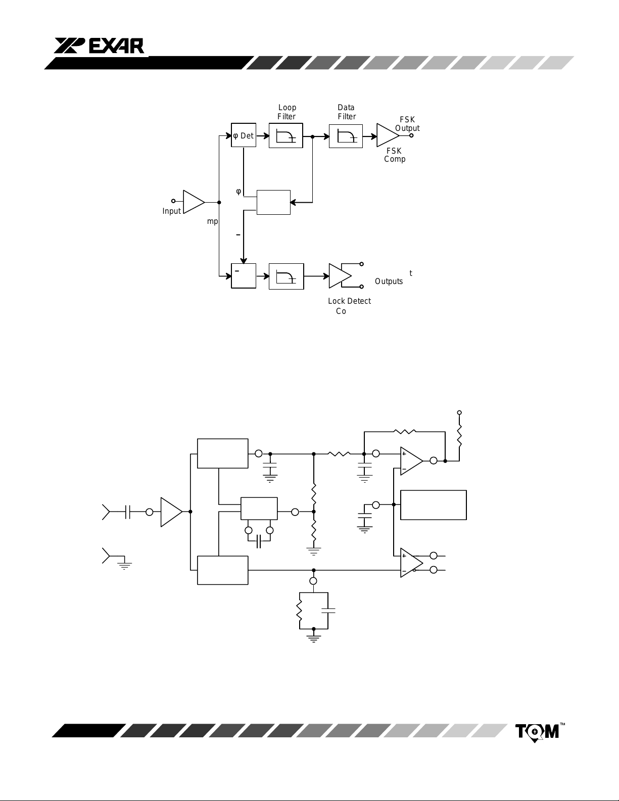
SYSTEM DESCRIPTION
The main PLL within the XR-221 1A is constructed from an
input preamplifier, analog multiplier used as a phase
detector and a precision voltage controlled oscillator
(VCO). The preamplifier is used as a limiter such that
input signals above typically 10mV rms are amplified to a
constant high level signal. The multiplying-type phase
detector acts as a digital exclusive or gate. Its output
(unfiltered) produces sum and difference frequencies of
the input and the VCO output. The VCO is actually a
current controlled oscillator with its normal input current
(f
) set by a resistor (R0) to ground and its driving current
O
with a resistor (R
) from the phase detector.
1
The output of the phase detector produces sum and
difference of the input and the VCO frequencies
Plastic Package 800mW. . . . . . . . . . . . . . . . . . . . . . . . .
Derate Above T
= 25°C 6mW/°C. . . . . . . . .
A
JEDEC SOIC 390mW. . . . . . . . . . . . . . . . . . . . . . . . . .
Derate Above T
= 25°C 5mW/°C. . . . . . . . . .
A
(internally connected). When in lock, these frequencies
are fIN+ f
VCO
(2 times f
when in lock) and fIN - f
IN
VCO
(0Hz
when lock). By adding a capacitor to the phase detector
output, the 2 times f
component is reduced, leaving a
IN
DC voltage that represents the phase difference between
the two frequencies. This closes the loop and allows the
VCO to track the input frequency.
The FSK comparator is used to determine if the VCO is
driven above or below the center frequency (FSK
comparator). This will produce both active high and
active low outputs to indicate when the main PLL is in lock
(quadrature phase detector and lock detector
comparator).
Rev. 1.04
5
Page 6

XR-2211A
PRINCIPLES OF OPERATION
Signal Input (Pin 2): Signal is AC coupled to this
terminal. The internal impedance at pin 2 is 20KW.
Recommended input signal level is in the range of 10mV
rms to 3V rms.
Quadrature Phase Detector Output (Pin 3): This is the
high impedance output of quadrature phase detector and
is internally connected to the input of lock detect voltage
comparator. In tone detection applications, pin 3 is
connected to ground through a parallel combination of R
and CD (see
Figure 3
) to eliminate the chatter at lock
detect outputs. If the tone detect section is not used, pin 3
can be left open.
Lock Detect Output, Q (Pin 6): The output at pin 6 is at
“low” state when the PLL is out of lock and goes to “high”
state when the PLL is locked. It is an open collector type
output and requires a pull-up resistor, R
, to VCC for
L
proper operation. At “low” state, it can sink up to 5mA of
load current.
Lock Detect Complement, (Pin 5): The output at pin 5 is
the logic complement of the lock detect output at pin 6.
This output is also an open collector type stage which can
sink 5mA of load current at low or “on” state.
FSK Data Output (Pin 7): This output is an open collector
logic stage which requires a pull-up resistor, R
, to VCC for
L
proper operation. It can sink 5mA of load current. When
decoding FSK signals, FSK data output is at “high” or “off”
state for low input frequency , and at “low” or “on” state for
high input frequency . If no input signal is present, the logic
state at pin 7 is indeterminate.
FSK Comparator Input (Pin 8): This is the high
impedance input to the FSK voltage comparator.
Normally, an FSK post-detection or data filter is
connected between this terminal and the PLL phase
detector output (pin 11). This data filter is formed by R
and CF (see
comparator is set by the internal reference voltage, V
Figure 3
). The threshold voltage of the
REF
available at pin 10.
Reference V oltage, V
biased at the reference voltage level, V
(Pin 10): This pin is internally
REF
: V
REF
REF
= VCC /2
- 650mV . The DC voltage level at this pin forms an internal
reference for the voltage levels at pins 5, 8, 1 1 and 12. Pin
10 must be bypassed to ground with a 0.1mF capacitor for
proper operation of the circuit.
Loop Phase Detector Output (Pin 11): This terminal
provides a high impedance output for the loop phase
detector. The PLL loop filter is formed by R
connected to pin 1 1 (see
Figure 3
). With no input signal, or
with no phase error within the PLL, the DC level at pin 1 1 is
very nearly equal to V
available at the phase detector output is equal to 2 x V
D
. The peak to peak voltage swing
REF
VCO Control Input (Pin 12): VCO free-running
frequency is determined by external timing resistor, R
connected from this terminal to ground. The VCO
free-running frequency, f
f
O
where C
is the timing capacitor across pins 13 and 14.
0
For optimum temperature stability, R
range of 10KW to 100KW (see
, is:
O
1
·
0
C
0
Hz
Figure 9
must be in the
0
).
R
This terminal is a low impedance point, and is internally
biased at a DC level equal to V
. The maximum timing
REF
current drawn from pin 12 must be limited to <
proper operation of the circuit.
VCO Timing Capacitor (Pins 13 and 14): VCO
frequency is inversely proportional to the external timing
capacitor, C
Figure 6
, connected across these terminals (see
0
). C0 must be non-polar, and in the range of
200pF to 10mF.
VCO Frequency Adjustment: VCO can be fine-tuned by
connecting a potentiometer, R
(see
Figure 10
).
VCO Free-Running Frequency , f
, in series with R0 at pin 12
X
: XR-221 1A does not
O
have a separate VCO output terminal. Instead, the VCO
outputs are internally connected to the phase detector
F
sections of the circuit. For set-up or adjustment purposes,
the VCO free-running frequency can be tuned by using
,
the generalized circuit in
Figure 3
, and applying an
alternating bit pattern of O’s and 1’s at the known mark
and space frequencies. By adjusting R
, the VCO can
0
then be tuned to obtain a 50% duty cycle on the FSK
output (pin 7). This will ensure that the VCO f
accurately referenced to the mark and space frequencies.
and C
1
3mA for
value is
O
REF
1
.
,
0
Rev. 1.04
6
Page 7
XR-2211A
Input
Preamp
Loop
Filter
φ
Det
φ
VCO
φ
φ
Det
Lock Detect
Filter
Data
Filter
Lock Detect
Comp
FSK
Output
FSK
Comp
Lock Detect
Outputs
Figure 2. Functional Block Diagram of a Tone and FSK Decoding System Using
XR-2211A
Input
Signal
0.1mF
V
CC
R
B
Loop
Phase
Detect
2
Quad
Phase
Detect
11
VCO
14 13
C
0
R
F
C
1
R
12
R
D
1
0.1mF
R
0
3
C
D
10
8
C
F
Lock
Detect
Comp.
7
FSK
Comp.
Internal
Reference
6
5
R
LDOQ
LDOQN
l
Figure 3. Generalized Circuit Connection for
FSK and Tone Detection
Rev. 1.04
7
Page 8

XR-2211A
DESIGN EQUATIONS
(All resistance in W, all frequency in Hz and all capacitance in farads, unless otherwise specified)
Figure 3
(See
1. VCO Center Frequency, f
for definition of components)
:
O
f
O
2. Internal Reference Voltage, V
V
REF
3. Loop Low-Pass Filter Time Constant, t:
+
where:
R
PP
if RF is or C
4. Loop Damping, j:
+
1
+
R
·
C
0
0
(measured at pin 10):
REF
V
CC
ǒ
R
ǒ
R
ǒ
2
(
seconds
PP
R
·
1
)
1
1250·
R
1
Ǔ
–
650
mV in volts
)
R
F
Ǔ
R
F
C
0
Ǔ
·
C
1
+
C
·
1
+
reactance is , then RPP = R1
F
Ǹ
Note: For derivation/explanation of this equation, please see T AN-011.
5. Loop-tracking
f
bandwidth,
f
f
0
f
LL
Rev. 1.04
"+
R
0
+
R
1
Df Df
f
1
f
0
Tracking
Bandwidth
f
f
O
2
f
LH
8
Page 9

XR-2211A
6. FSK Data filter time constant, tF:
R
·
R
B
t
+
F
(
R
7. Loop phase detector conversion gain, Kd: (Kd is the differential DC voltage across pin 10 and pin11, per unit of
phase error at phase detector input):
V
+
d
REF
10,000·p
K
Note: For derivation/explanation of this equation, please see T AN-011.
8. VCO conversion gain, Ko: (Ko is the amount of change in VCO frequency , per unit of DC voltage change at pin 1 1):
F
·
C
(
B
F
·
R
volt
1
ƪ
radian
ƫ
seconds
F
)
)
R
)
–
V
·
O
(
2p
·
C
·
R
0
REF
1 )
K
·F(s) +
d
V
REF
1
1
SR
·
C
1
in volts and IAin amps
K
+
0
9. The filter transfer function:
F(s
) +
10. Total loop gain. KT:
K
+
K
T
11. Peak detector current IA:
V
+
REF
20,000
I
A
Note: For derivation/explanation of this equation, please see T AN-011.
radianńsecond
ǒ
+
at0Hz
1
ǒ
5,000·
volt
.
R
F
C
·(
R
0
1
Ǔ
S = Jw and w = 0
ƪ
Ǔ
R
)
F
)
seconds
)
1
ƫ
Rev. 1.04
9
Page 10

XR-2211A
APPLICATIONS INFORMATION
FSK Decoding
Figure 10
of external components are defined as follows: R
and C
the FSK data output. The resistor R
shows the basic circuit connection for FSK decoding. With reference to
and C0 set the PLL center frequency , R1 sets the system bandwidth,
0
sets the loop filter time constant and the loop damping factor. CF and RF form a one-pole post-detection filter for
1
from pin 7 to pin 8 introduces positive feedback across the FSK comparator to
B
Figure 3
and
Figure 10
, the functions
facilitate rapid transition between output logic states.
Design Instructions:
The circuit of
R
, C0, C1 and CF. For a given set of FSK mark and space frequencies, fO and f1, these parameters can be calculated as
1
Figure 10
can be tailored for any FSK decoding application by the choice of five key circuit components: R0,
follows:
(All resistance in W’s, all frequency in Hz and all capacitance in farads, unless otherwise specified)
a) Calculate PLL center frequency, f
Ǹ
f
+
F
·
F
1
O
2
:
O
b) Choose value of timing resistor R0, to be in the range of 10KW to 100KW. This choice is arbitrary . The recommended
value is R
c) Calculate value of C0 from design equation (1) or from
= 20KW. The final value of R0 is normally fine-tuned with the series potentiometer, RX.
0
R
R
+
R
O
X
)
O
2
Figure 7
:
+
1
R
·
f
0
0
C
O
d) Calculate R1 to give the desired tracking bandwidth (See design equation 5).
R
·
f
0
(
f1–f
0
·2
)
2
R
+
1
e) Calculate C1 to set loop damping. (See design equation 4):
Normally, j = 0.5 is recommended.
1250·
C
C
Rev. 1.04
+
1
0
2
R
·
1
10
Page 11

XR-2211A
f) The input to the XR-221 1A may sometimes be too sensitive to noise conditions on the input line.
Figure 4
illustrates
a method of de-sensitizing the XR-221 1A from such noisy line conditions by the use of a resistor, Rx, connected
from pin 2 to ground. The value of Rx is chosen by the equation and the desired minimum signal threshold level.
VINminimum(peak
) +
Va–V
+
b
V
" 2.8
mV offset+V
REF
(20,000 )
20,000
or R
+ 20,000
R
X
X
)
V
REF
ǒ
–
V
VIN minimum (peak) input voltage must exceed this value to be detected (equivalent to adjusting V threshold)
V
CC
To Phase
Detector
Input
Rx
Va
2
20K
10
V
REF
Vb
20K
Ǔ
1
Figure 4. Desensitizing Input Stage
g) Calculate Data Filter Capacitance, CF:
(
+
R
(
R
1
(
R
·
sum
R
sum
C
+
F
Note: All values except R0 can be rounded to nearest standard value.
)
)
R
·
R
1
F
)
R
)
R
F
0.25
Baud Rate
B
)
B
)
Baud rate in
1
seconds
Rev. 1.04
11
Page 12

XR-2211A
20
15
R0=5KΩ
10
=10KΩ
R
0
5
Supply vs. Current (mA)
0
4681012141618202224
Supply Voltage, V
R
0
+
(Volts)
>100K
Figure 5. Typical Supply Current vs. V+
(Logic Outputs Open Circuited)
1,000
C0=0.001mF
C0=0.0033mF
W
100
0
R (K )
10
C0=0.1mF
C0=0.33mF
0 1000 10000
C0=0.01mF
C0=0.0331mF
fO(Hz)
Figure 7. VCO Frequency vs. Timing Capacitor
1.0
R0=5KW
R0=10KW
m
0.1
0
C ( F)
0.01
100 1000 10000
R0=20KW
R0=40KW
R0=80KW
R0=160KW
f
(HZ)
O
Figure 6. VCO Frequency vs. Timing Resistor
1.02
5
1.01
4
1.00
3
0.99
2
0.98
Normalized Frequency
1
0.97
4 6 8 10 12 14 16 18 20 22 24
Figure 8. Typical f
f
= 1kHz
O
= 10R
R
F
0
V+ (Volts)
vs. Power Supply
O
Curve
1
2
3
4
5
2
100K
300K
4
R
5K
10K
30K
1
0
Characteristics
5
3
Rev. 1.04
O
+1.0
R0=10K
+0.5
R0=50K
0
R0=500K
-0.5
R0=1MΩ
-1.0
Normalized Frequency Drift (% of f )
-50 -25 0 25 50 75 100 125
Temperature (°C)
V+ = 12V
R1 = 10 R
f
= 1 kHz
O
1MΩ
500K
50K
10K
0
Figure 9. Typical Center Frequency Drift vs. Temperature
12
Page 13

Design Example:
1200 Baud FSK demodulator with mark and space frequencies of 1200/2200.
XR-2211A
Step 1: Calculate f
(
a)f
Step 2: Calculate R0 : R
(
b)R
Step 3: Calculate C
c)C
(
: from design instructions
O
Ǹ
+ 1200·2200
O
0
+ 10)
T
from design instructions
0
+
O
15000·1624
=1624
=10K with a potentiometer of 10K. (See design instructions (b))
10
ǒ
Ǔ
+ 15
2
1
K
+ 39
nF
Step 4: Calculate R1 : from design instructions
(
d)R
Step 5: Calculate C
(
e)C
20000·1624·2
+
1
(
2200–1200
: from design instructions
1
1250·39
+
1
51000·0.5
nF
2
)
+ 3.9
+ 51,000
nF
Step 6: Calculate RF : RF should be at least five times R1, RF = 51,000⋅5 = 255 KW
Step 7: Calculate R
Step 8: Calculate R
Step 9: Calculate C
Note: All values except R
Rev. 1.04
: RB should be at least five times RF, RB = 255,000⋅5 = 1.2 MW
B
SUM :
(
R
SUM
C
+
F
R
+
(
R
F
F :
ǒ
R
·
SUM
can be rounded to nearest standard value.
0
)
)
R
·
R
1
F
)
R
)
R
1
0.25
Baud Rate
B
B
+ 240
)
+ 1
Ǔ
nF
K
13
Page 14

XR-2211A
Input
Signal
2
0.1µF
Loop
Phase
Detect
Quad
Phase
Detect
11
VCO
14
27nF 5%
V
CC
R
B
1.8m 5%
1nF
VCO
Fine
Tune
8
C
10%
10
7
F
FSK
Comp.
Internal
Reference
RF178K
C
1
2.7nF
5%
12
13
C
O
5%
R
1
35.2K
1%
R
0
20K
1%
Rx
20K
0.1µF
R
L
5.1K
5%
Data
Output
6
LDOQ
LDOQN
Lock
Detect
Comp.
5
Figure 10. Circuit Connection for FSK Decoding of Caller Identification Signals
(Bell 202 Format)
V
R
B
Input
Signal
2
0.1µF
Between 400K and 600K
Loop
Phase
Detect
14 13
Quad
Phase
Detect
11
VCO
C
R
C
1
R
12
1
0.1µF
R
0
0
Rx
3
R
D
8
F
C
F
10
FSK
Comp.
Internal
7
Reference
6
LDOQ
LDOQN
5
Lock
Detect
C
D
Comp.
CC
R
L
5.1k
Rev. 1.04
Figure 11. External Connectors for FSK Demodulation with Carrier
Detect Capability
14
Page 15

XR-2211A
V
CC
Loop
Phase
Detect
2
0.1µF
Tone
Input
Quad
Phase
Detect
Figure 12. Circuit Connection for Tone Detection
FSK Decoding with Carrier Detect
14
11
VCO
50nF
8
C
1
220pF
5%
12
13
C
0
5%
R
470K
R
1
200K
1%
R
0
20K
1%
Rx
5K
3
D
0.1µF
VCO
Fine
Tune
C
80nF
10
Detect
D
+
Reference
+
Lock
Comp.
7
FSK
Comp.
Internal
6 LDOQ
5 LDOQN
V
CC
RL2
5.1K
RL3
5.1K
Logic Output
The lock detect section of XR-2211A can be used as a
carrier detect option for FSK decoding. The
recommended circuit connection for this application is
shown in
Figure 11.
The open collector lock detect output,
pin 6, is shorted to data output (pin 7). Thus, data output
will be disabled at “low” state, until there is a carrier within
the detection band of the PLL and the pin 6 output goes
“high” to enable the data output.
Note: Data Output is “Low” When No Carrier is Present.
The minimum value of the lock detect filter capacitance
is inversely proportional to the capture range, +Dfc.
C
D
This is the range of incoming frequencies over which the
loop can acquire lock and is always less than the tracking
range. It is further limited by C1. For most applications, Dfc
> Df/2. For R
of C
can be determined by:
D
= 470KW, the approximate minimum value
D
16
C
§
D
C in F and f in Hz.
f
C in mF and f in Hz.
With values of C
that are too small, chatter can be
D
observed on the lock detect output as an incoming signal
frequency approaches the capture bandwidth.
Excessively large values of C
will slow the response time
D
of the lock detect output. For Caller I.D. applications
choose C
= 0.1mF.
D
Tone Detection
Figure 12
shows the generalized circuit connection for
tone detection. The logic outputs, LDOQN and LDOQ at
pins 5 and 6 are normally at “high” and “low” logic states,
respectively . When a tone is present within the detection
band of the PLL, the logic state at these outputs become
reversed for the duration of the input tone. Each logic
output can sink 5mA of load current.
Both outputs at pins 5 and 6 are open collector type
stages, and require external pull-up resistors R
R
, as shown in
L3
With reference to
Figure 12.
Figure 3
and
Figure 12
, the functions of
L2
and
the external circuit components can be explained as
follows: R
detection bandwidth; C
and C0 set VCO center frequency; R1 sets the
0
sets the low pass-loop filter time
1
constant and the loop damping factor.
Rev. 1.04
15
Page 16

XR-2211A
Design Instructions:
The circuit of
R
, R1, C0, C1 and CD. For a given input, the tone frequency, fS, these parameters are calculated as follows:
0
Figure 12
can be optimized for any tone detection application by the choice of the 5 key circuit components:
(All resistance in W’s, all frequency in Hz and all capacitance in farads, unless otherwise specified)
a) Choose value of timing resistor R
current that the internal voltage reference can deliver. The recommended value is R
is normally fine-tuned with the series potentiometer, R
b) Calculate value of C
C
1
+
O
R
0
from design equation (1) or from
0
·
fs
to be in the range of 10KW to 50KW. This choice is dictated by the max./min.
0
= 20KW. The final value of R0
0
.
X
Figure 7
fS = fO:
c) Calculate R1 to set the bandwidth +Df (See design equation 5):
R
·
f
·2
0
R
+
1
Note: The total detection bandwidth covers the frequency range of fO +Df
0
f
D
d) Calculate value of C1 for a given loop damping factor:
Normally, j = 0.5 is recommended.
1250·
C
C
+
1
0
2
R
·j
1
Increasing C
e) Calculate value of the filter capacitor C
C
improves the out-of-band signal rejection, but increases the PLL capture time.
1
. To avoid chatter at the logic output, with RD = 470KW, C
D
16
§
D
D
f
CinmF
Increasing CD slows down the logic output response time.
Design Examples:
Tone detector with a detection band of +
a) Choose value of timing resistor R
100Hz:
to be in the range of 10KW to 50KW. This choice is dictated by the max./min.
0
current that the internal voltage reference can deliver. The recommended value is R
is normally fine-tuned with the series potentiometer, R
b) Calculate value of C
C
1
+
0
R
0
from design equation (1) or from
0
+
·
f
S
1
20,000·1,000
+ 50
nF
.
X
Figure 6
fS = fO:
must be:
D
= 20 KW. The final value of R0
0
Rev. 1.04
16
Page 17

c) Calculate R1 to set the bandwidth +Df (See design equation 5):
R
·
f
·2
0
R
+
1
O
f
20,000·1,000·2
+
100
+ 400
K
Note: The total detection bandwidth covers the frequency range of fO +f
d) Calculate value of C0 for a given loop damping factor:
Normally, j = 0.5 is recommended.
–
1250·
C
+
1
C
2
R
·
1
0
+
1250·50·10
400,000·0.5
9
+ 6.25
2
pF
Increasing C1 improves the out-of-band signal rejection, but increases the PLL capture time.
XR-2211A
e) Calculate value of the filter capacitor C
16
C
+
D
16
w
f
200
w 80
nF
. To avoid chatter at the logic output, with RD = 470KW, CD must be:
D
Increasing CD slows down the logic output response time.
f) Fine tune center frequency with 5KW potentiometer, R
V
CC
8
10
FM
Input
0.1µF
Loop
Phase
Detect
2
Quad
Phase
Detect
14
11
VCO
C
1
R
12
13
C
0
1
0.1µF
R
0
X
.
Comp
.
Internal
Reference
Lock
Detect
Comp.
7
FSK
6
5
R
F
100K
LDOQ
LDOQN
V
CC
0.1µF
4
3
C
F
2
1
LM324
11
Demodulated
Output
Rev. 1.04
Figure 13. Linear FM Detector Using XR-2211A and an External Op Amp.
(See Section on Design Equation for Component Values.)
17
Page 18

XR-2211A
Linear FM Detection
XR-221 1A can be used as a linear FM detector for a wide
range of analog communications and telemetry
applications. The recommended circuit connection for
this application is shown in
Figure 13.
The demodulated
output is taken from the loop phase detector output (pin
1 1), through a post-detection filter made up of R
and CF,
F
and an external buffer amplifier. This buffer amplifier is
necessary because of the high impedance output at pin
11. Normally, a non-inverting unity gain op amp can be
used as a buffer amplifier, as shown in
+
V
1
20K
20K
REF
Voltage
Output
10
Figure 13.
Input
2
10K 10K
The FM detector gain, i.e., the output voltage change per
unit of FM deviation can be given as:
R
·
V
1
V
OUT
where VR is the internal reference voltage (V
100·
REF
R
0
REF
- 650mV). For the choice of external components R
, C1 and CF, see the section on design equations.
C
D
Lock
Detect
B
From
VCO
B’
Filter
3
= VCC /2
, R0,
1
6
Lock Detect
Outputs
5
4
Ground
Rev. 1.04
Internal Voltage
Reference
2K
A
Timing
Capacitor
13
B
Timing
R
0
Resistor
Voltage Controlled
Oscillator
Input Preamplifier
and Limiter
2K
A’
14
C
0
B’
12
8K
From
VCO
A
A’
Loop Phase Detector
Quadrature
Phase Detector
11
Loop
Detector
Output
8
FSK
Comparator
Input
FSK Comparator
Lock Detect
Comparator
7
FSK
Data
Output
Figure 14. Equivalent Schematic Diagram
18
Page 19

14 LEAD PLASTIC DUAL-IN-LINE
(300 MIL PDIP)
Rev. 1.00
XR-2211A
Seating
Plane
14
1
D
A
L
B
SYMBOL MIN MAX MIN MAX
A 0.145 0.210 3.68 5.33
A
1
A
2
B 0.014 0.024 0.36 0.56
B
1
C 0.008 0.014 0.20 0.38
D 0.725 0.795 18.42 20.19
E 0.300 0.325 7.62 8.26
E
1
e 0.100 BSC 2.54 BSC
e
A
e
B
L 0.115 0.160 2.92 4.06
e
INCHES
0.015 0.070 0.38 1.78
0.115 0.195 2.92 4.95
0.030 0.070 0.76 1.78
0.240 0.280 6.10 7.11
0.300 BSC 7.62 BSC
0.310 0.430 7.87 10.92
8
E
1
1
A
1
MILLIMETERS
7
B
α 0° 15° 0° 15°
Note: The control dimension is the inch column
E
A
2
α
e
A
e
B
C
Rev. 1.04
19
Page 20

XR-2211A
14 LEAD SMALL OUTLINE
(150 MIL JEDEC SOIC)
Rev. 1.00
D
14 8
E H
1
7
Seating
Plane
C
A
e
SYMBOL MIN MAX MIN MAX
A 0.053 0.069 1.35 1.75
A
1
B 0.013 0.020 0.33 0.51
C 0.007 0.010 0.19 0.25
D 0.337 0.344 8.55 8.75
E 0.150 0.157 3.80 4.00
e 0.050 BSC 1.27 BSC
H 0.228 0.244 5.80 6.20
L 0.016 0.050 0.40 1.27
α 0
Note: The control dimension is the millimeter column
1
B
INCHES MILLIMETERS
0.004 0.010 0.10 0.25
° 8° 0° 8°
A
α
L
Rev. 1.04
20
Page 21

Notes
XR-2211A
Rev. 1.04
21
Page 22

XR-2211A
Notes
Rev. 1.04
22
Page 23

Notes
XR-2211A
Rev. 1.04
23
Page 24

XR-2211A
NOTICE
EXAR Corporation reserves the right to make changes to the products contained in this publication in order to improve design, performance or reliability . EXAR Corporation assumes no responsibility for the use of any circuits described herein, conveys no license under any patent or other right, and makes no representation that the circuits are
free of patent infringement. Charts and schedules contained here in are only for illustration purposes and may vary
depending upon a user’s specific application. While the information in this publication has been carefully checked;
no responsibility, however, is assumed for inaccuracies.
EXAR Corporation does not recommend the use of any of its products in life support applications where the failure or
malfunction of the product can reasonably be expected to cause failure of the life support system or to significantly
affect its safety or effectiveness. Products are not authorized for use in such applications unless EXAR Corporation
receives, in writing, assurances to its satisfaction that: (a) the risk of injury or damage has been minimized; (b) the
user assumes all such risks; (c) potential liability of EXAR Corporation is adequately protected under the circumstances.
Copyright 1995 EXAR Corporation
Datasheet June 1997
Reproduction, in part or whole, without the prior written consent of EXAR Corporation is prohibited.
Rev. 1.04
24
 Loading...